power devices - technische universität münchen · pdf file2 power devices in power...
TRANSCRIPT

1
„Power Devices“
Prof. Dr.‐Ing. Hans‐Georg Herzog([email protected])
Prof. Dr.‐Ing. Ralph Kennel([email protected])
Technische Universität MünchenArcisstraße 21
80333 MünchenGermany

2
Power Devicesin power electronics active operation of power semiconductor devices is avoided
• either the voltage at the device is 0
• or the current in the device is 0
unfortunately power semiconductor devices are no ideal switches!
→ what requirements have to be postulated ?
switch off switching event switch on
• low blocking current • low switching losses • low voltage drop
• bidirectional blocking • short switching time • bidirectional conduction
• high blocking voltage • free control oftime of switching
• high current capability
• high du/dt • no snubber circuits • high di/dt

3
Losses in Real Power Semiconductor Devices
switch-onlosses
switch-offlosses
conductionlosses

4
Hard Switching Devices
• high stress on semiconductor• wide SOA (safe operation area) necessary• low switching frequency• problematic with respect to high power

5
Soft Switching Devices
• low stress on semiconductor• high switch-off current possible• high switching frequency• simple gate driving circuits• additional power components necessary

6
IGBT Turn-Off with Snubberhard switching
Eoff = 226µJ Eoff = 98µJ
with snubber
current “pops up”
but losses are still greatly reduced in the semiconductor
the overall losses, however, increase
Gate voltage
Collector current
Collector voltage
Gate voltage
Collector current
Collector voltage
400V, 20A, 125°C, RG = 9.1Ω

7
„Power Devices“
Diode(Thyristor, GTO, IGCT)
Referents:Prof. Dr.‐Ing. Hans‐Georg Herzog
([email protected])Prof. Dr.‐Ing. Ralph Kennel
([email protected])Technische Universität München
Arcisstraße 2180333 München
Germany

8
Power Diode Characteristic

9
Power Diode Switching-Off Behaviour

10
PIN - Diode… to ensure a sufficient voltage capability …
… the junction area is increased in distance…
… by introducing a so-called „intrinsisc“ layer
(= semiconductor material without any doping)
between the p-doped and the n-doped layer …
PIN - Diode
p nii

11
ThyristorStructure
ACA
A
12
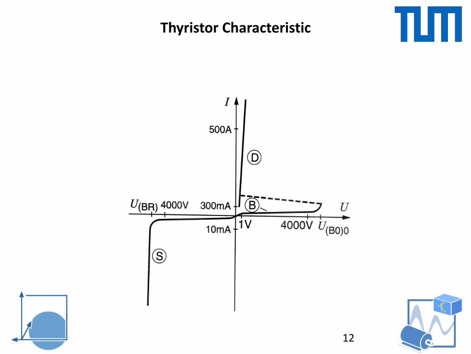
Thyristor Characteristic

13
Triac

14
/ GTO
standard thyristortechnology
single waferuntil 150 mm
low conductionlosses
high currentcapability
high switching losses
high powerfor driver circuit

15
GTO IGCT
both are controllable thyristors –
however, according to different philosophies
GTOearlier in the market
switch-off concept :by deviating
a part of the load current (ca. 30 %) via the gate
filigrane structure on the chip
IGCT(too) late in the market
switch-off concept :by deviating
the full load currentvia the gate
very complex driver circuits

16
„Power Devices“
(bipolar) Transistor
Referents:Prof. Dr.‐Ing. Hans‐Georg Herzog
([email protected])Prof. Dr.‐Ing. Ralph Kennel
([email protected])Technische Universität München
Arcisstraße 2180333 München
Germany

17
Bipolar Power Transistor

18
Switch-On Behaviour of a Bipolar Power Transistors

19
Switch-Off Behaviour of a Bipolar Power Transistors
20
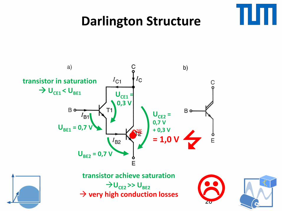
Darlington Structure
UBE1 = 0,7 V
UCE1 =0,3 V
UBE2 = 0,7 V
UCE2 =0,7 V+ 0,3 V
= 1,0 V
transistor in saturation UCE1 < UBE1
transistor achieve saturationUCE2 >> UBE2
very high conduction losses

21
„Power Devices“
Field Effect Transistor (FET)
Referents:Prof. Dr.‐Ing. Hans‐Georg Herzog
([email protected])Prof. Dr.‐Ing. Ralph Kennel
([email protected])Technische Universität München
Arcisstraße 2180333 München
Germany

22
Field Effect Transistor (MOSFET)Structure
channel : long and thin high internal resistance

23
channel : still thin - but not as long any more
low internal resístance
Field Effect Transistor (MOSFET)Structure

24
Field Effect Transistor (MOSFET) parasitic pnp-transistor

25
Field Effect Transistor (MOSFET) parasitic capacitances

26
„Power Devices“
Insulated Gate Bipolar Transistor (IGBT)
Referents:Prof. Dr.‐Ing. Hans‐Georg Herzog
([email protected])Prof. Dr.‐Ing. Ralph Kennel
([email protected])Technische Universität München
Arcisstraße 2180333 München
Germany

27
Insulated Gate Bipolar Transistor (IGBT)Structure

28
Insulated Gate Bipolar Transistor (IGBT)Structure and Equivalent Circuit
bipolar pnp-transistor
Think of it as a MOSFET with low conduction loss.

29
Insulated Gate Bipolar Transistor (IGBT)parasitic capacitances

30
Insulated Gate Bipolar Transistor (IGBT)parasitic (latch-up) transistor

31
MOSFETtechnology
chip size until20 x 20 mm²
low powerfor driver circuit
low switching losses
high voltage drop
contactingproblems

32TECHNOLOGY TO THE NEXT POWER
On-State Voltage Comparison – Same Die Size
•IGBT has lower on-voltage above about 4 Amps.
•MOSFET conduction loss is sensitive to temperature, the IGBT is not.
•APT6038BLL: ID = 17A
•APT30GP60B: IC2 = 49A
MOSFET 125 °C
MOSFET 25 °C
IGBT
On-State Voltage vs. Current
0
10
20
30
40
50
60
0 10 20 30 40
Current (A)
Vo
ltag
e (
V)
APT6038BLL (25 °C) APT30GP60B (25 or 125 °C)
APT6038BLL (125 °C)

33TECHNOLOGY TO THE NEXT POWER
Conduction Loss Comparison – Same Die Size
•IGBT has much lower conduction loss above about 4 Amps.
•IGBT has much better overload capability.
Conduction Loss vs. Current (125 °C)
0
200
400
600
800
1000
1200
1400
0 5 10 15 20 25 30 35 40
Current (A)
Po
wer
(W)
APT6038BLL APT30GP60B
MOSFET
IGBT
3434
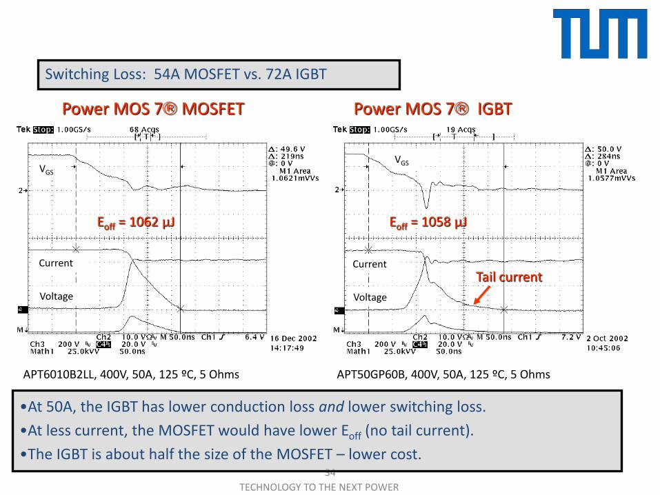
Power MOS 7MOSFET Power MOS 7 IGBT
APT6010B2LL, 400V, 50A, 125 ºC, 5 Ohms APT50GP60B, 400V, 50A, 125 ºC, 5 Ohms
Switching Loss: 54A MOSFET vs. 72A IGBT
Eoff = 1062 µJ Eoff = 1058 µJ
•At 50A, the IGBT has lower conduction loss and lower switching loss.
•At less current, the MOSFET would have lower Eoff (no tail current).
•The IGBT is about half the size of the MOSFET – lower cost.
Tail currentCurrent
Voltage
VGS
Current
Voltage
VGS
TECHNOLOGY TO THE NEXT POWER

35TECHNOLOGY TO THE NEXT POWER
Frequency vs. Current
0
100
200
300
400
500
5 10 15 20 25 30
Current (Amps)
Fre
qu
en
cy (
kH
z)
APT15GP60B APT6029BLL
Application Comparison – Hard Switched Boost
MOSFET is best at low current, very high frequency.IGBT is best at high current.IGBT is lower cost.
IGBT
MOSFET
Boost: Hard switched
400V, TJ = 125 C, TC = 75 C, 5
APT15GP60: IC2 = 30A
APT6029: ID = 21A
MOSFET is 2.5 times larger than IGBT.
IGBT has good overload capability.

36
Advantage of IGBTs
• Lower cost – much smaller die size for same power.
• Excellent overload capability – linear conduction loss versus current, very insensitive to temperature.
• Simple gate drive – can replace MOSFETs – positive only gate drive
• Highest speed IGBTs – turn-on is the same as a MOSFET, turn-off is only slightly longer.
• Suitable for soft and hard switching – zero voltage or reduced voltage turn-off not as good as MOSFETs.
TECHNOLOGY TO THE NEXT POWER

37
Parallel Connection of IGBTs
• additional resistors in series
• semiconductor design with integrated path
with a positive temperature coefficient

38
39

40
Siliziumkarbid (SiC)

41
Reasons for Wide Band Gap Devices Added Value and Related Impact
source :Pierric Gueguen, Market & Technology Overview of Power Electronics Industry and Impact of
WBG Devices, Yole Développement, SEMICON Europa 2014, Grenoble, 09.10.2014

42
Quelle : Teresa Bertelshofer; Universität Erlangen

43
Quelle : Teresa Bertelshofer; Universität Erlangen

44
Quelle : Teresa Bertelshofer; Universität Erlangen

45
Quelle : Teresa Bertelshofer; Universität Erlangen

46
Quelle : Teresa Bertelshofer; Universität Erlangen

47
Quelle : Teresa Bertelshofer; Universität Erlangen

48
Quelle : Teresa Bertelshofer; Universität Erlangen

49
Comparison Si SiC(switching) losses
source : www.infineon.com/sic; Power Electronics Europe ; Issue 6 2009„Efficiency Improvement with Silicon Carbide Based Power Modules“

50
Quelle : Teresa Bertelshofer; Universität Erlangen

51
Quelle : Teresa Bertelshofer; Universität Erlangen

52
SiC Device Application Roadmapsource :
Pierric Gueguen, Market & Technology Overview of Power Electronics Industry and Impact of WBG Devices, Yole Développement, SEMICON Europa 2014, Grenoble, 09.10.2014

53

54
Silicon Carbide (SiC)
• better (faster ?) switching
• higher temperature robustness
• voltage drops ?
• cannot be produced on
„outsourced“ production lines for memory chips
investment cost not negligible

55
Key Characteristics of GaN vs. SiC vs. Sisource : ECPE

56
„Power Devices“
Mechanical Design andCooling Techniques
Referents:Prof. Dr.‐Ing. Hans‐Georg Herzog
([email protected])Prof. Dr.‐Ing. Ralph Kennel
([email protected])Technische Universität München
Arcisstraße 2180333 München
Germany

57
Power Module and Disc Design

58
Housings
plastic
aluminium
silicon
aluminium
AlN substrate
soldering
simple mounting (screws)insulation to groundsuitable for single chipsundefined fault behaviourexplosion posiible
copper
molybdenium
aluminium
silicon
Aluminium
metal substr.
copper
Power Module
Disc Design double sided coolingfault shortcutsuitable for series connectionlow flexibilitymechanical provisions
for pressing

59
Insulated Gate Bipolar Transistor (IGBT)Mechanical Design

60
Driver Circuits

61
Cooling Techniques
Cooling of Power Devices
• thermâl equivalent circuit
• natural convection
• forced air cooling
• liquid cooling

62
Electrical Equivalent Circuitfor Modelling of Thermal Behaviour
Dualism :heat source current sourcethermal energy currenttemperature electrical potentialtemperature difference voltagethermal resistance electrical resistanceheat capacitance electrical capacitancedoes not exist electrical inductance
… therefore temperature can physically not „oscillate“

63
… in case of simple heat distributions of low complexitythe components of the equivalent circuit can be calculated
from the geometry of the design and the physical parameters of the material
… for more complex heat distributionsFEM simulation software is available in the market
… like in the case of electrical resistors
Elektrical Equivalent Circuitfor Modelling of Thermal Behaviour

64
Alternative : by measurement as in the analysis of electrical circuits
… e. g. by measuring step response(s)
Elektrical Equivalent Circuitfor Modelling of Thermal Behaviour

65
advantage of electrical equivalent circuit :
transient heat dissipation can be calculated simplyby methods of network theory and signal analysis
Elektrical Equivalent Circuitfor Modelling of Thermal Behaviour

66
natural convectionheat transfer from heat sink
to surrounding airdepends on :
temperature difference„active“ surface speed of airflow
… therefore the heat sink must …
contain materialof good thermal conductivity
(aluminium, copper etc.) thick root and as many ribs as possible
provide surface as wide as possible(mostly as aluminium profile)
have a dark surfacebe mounted vertically
(chimney effect)

67
more designs of heat sinks
• punched and molded sheet metal
• plug-on star-shaped or flag-like heat sink
– made of aluminium
– made of phosphorus bronze
– made of sheet steel
• base plate made of aluminium,
with pressed in cooling sheets

68
in comparison to natural cooling (convection)the thermal resistance of the heat sink
can be reduced to 1/5 ... 1/15by forced air cooling
with respect to the major part of convectionin the cooling
a black/dark surface does not really have an effectin case of forced air cooling
Forced Air Cooling

69
Liquid Cooling
lower temperature drop betweenheat sink surface and cooling liquid
higher power transfer or lower temperature of the chip
(long life time)
with respect to ist high thermal capacitance(specific heat cp = 4,187 kJ/kg *K)
water is suitable for heat transfermore than other liquids (oil or glycol)
70
Liquid Cooling in the Cooling System of a Vehicle:
by additional mixing of e. g. glycolthe thermal capacitance of the liquid is reduced
at the same time viscosity and specific weight of the cooling liquid increases
with increasing percentage of glycolthermal resistance between heat sink and cooling liquid increases significantly
50 % glycol addition increase of Rthhw by 50...60 %90 % glycol addition increase of Rthhw by 110...130 %
Liquid Cooling

71
Heatpipes are for heat transport
… are used,to transmit the heat from a device
to the heat sink(e. g. in case of cramped space condition)
... improve the temperature distributionas well as the dynamic behaviour
Liquid Cooling by Heat Pipes