power dissipation and its linear derating factor, … 2006 rev 1 1/14 an2385 application note power...
TRANSCRIPT

June 2006 Rev 1 1/14
AN2385Application note
Power dissipation and its linear derating factor, siliconLimited Drain Current and pulsed drain current in MOSFETs
IntroductionDatasheets of the modern power MOSFET devices, either of low voltage or of high voltage, show in the section entitled "Absolute Maximum Rating" the values of some important parameters that regard the SOA (safe operating area). As it is well kwown in literature, SOA is the area that includes all the ID-VDS operating points where the device works in safety conditions.
These important parameters are studied in this technical article. In particular, attention will be focused on the Power Dissipation and its Linear Derating Factor, Silicon Limited Drain Current and Pulsed Drain Current. This technical article will explain what these parameters are and how they can be calculated. It will recall some basic and simple technical concepts and can be a useful tool for customers to understand and facilitate reading of a power MOSFET datasheet.
www.st.com

Contents AN2385
2/14
Contents
1 Determination of the SOA limits . . . . . . . . . . . . . . . . . . . . . . . . . . . . . . . 5
2 Silicon limited drain current . . . . . . . . . . . . . . . . . . . . . . . . . . . . . . . . . . . 7
3 Determination of the power dissipation and its derating factor . . . . . . 9
4 Pulsed drain current (IDM) . . . . . . . . . . . . . . . . . . . . . . . . . . . . . . . . . . . 10
5 Conclusions . . . . . . . . . . . . . . . . . . . . . . . . . . . . . . . . . . . . . . . . . . . . . . . 12
6 Revision history . . . . . . . . . . . . . . . . . . . . . . . . . . . . . . . . . . . . . . . . . . . 13
AN2385 List of figures
3/14
List of figures
Figure 1. Typical FBSOA of a Power MOSFET . . . . . . . . . . . . . . . . . . . . . . . . . . . . . . . . . . . . . . . . . . 5Figure 2. RDSON limit for MOSFET's FBSOA . . . . . . . . . . . . . . . . . . . . . . . . . . . . . . . . . . . . . . . . . . . 6Figure 3. Typical RBSOA of a Power MOSFET. . . . . . . . . . . . . . . . . . . . . . . . . . . . . . . . . . . . . . . . . . 6Figure 4. Silicon limited drain current vs case temperature . . . . . . . . . . . . . . . . . . . . . . . . . . . . . . . . . 8Figure 5. Power dissipation vs T . . . . . . . . . . . . . . . . . . . . . . . . . . . . . . . . . . . . . . . . . . . . . . . . . . . . . 9Figure 6. IDM determination considering the output characteristic . . . . . . . . . . . . . . . . . . . . . . . . . . 10Figure 7. Junction to case maximum effective transient thermal impedance for TO-220 package.. . 10Figure 8. Determination of the maximum rectangular pulse duration . . . . . . . . . . . . . . . . . . . . . . . . 11

List of tables AN2385
4/14
List of tables
Table 1. Revision history . . . . . . . . . . . . . . . . . . . . . . . . . . . . . . . . . . . . . . . . . . . . . . . . . . . . . . . . . 13
AN2385 Determination of the SOA limits
5/14
1 Determination of the SOA limits
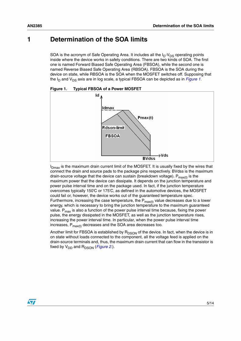
SOA is the acronym of Safe Operating Area. It includes all the ID-VDS operating points inside where the device works in safety conditions. There are two kinds of SOA. The first one is named Forward Biased Safe Operating Area (FBSOA), while the second one is named Reverse Biased Safe Operating Area (RBSOA). FBSOA is the SOA during the device on state, while RBSOA is the SOA when the MOSFET switches off. Supposing that the ID and VDS axis are in log scale, a typical FBSOA can be depicted as in Figure 1.
Figure 1. Typical FBSOA of a Power MOSFET
IDmax is the maximum drain current limit of the MOSFET. It is usually fixed by the wires that connect the drain and source pads to the package pins respectively. BVdss is the maximum drain-source voltage that the device can sustain (breakdown voltage). Pmax(t) is the maximum power that the device can dissipate. It depends on the junction temperature and power pulse interval time and on the package used. In fact, if the junction temperature overcomes typically 150'C or 175'C, as defined in the automotive devices, the MOSFET could fail or, however, the device works out of the guaranteed temperature spec. Furthermore, increasing the case temperature, the Pmax(t) value decreases due to a lower energy, which is necessary to bring the junction temperature to the maximum guaranteed value. Pmax is also a function of the power pulse interval time because, fixing the power pulse, the energy dissipated in the MOSFET, as well as the junction temperature rises, increasing the power interval time. In particular, when the power pulse interval time increases, Pmax(t) decreases and the SOA area decreases too.
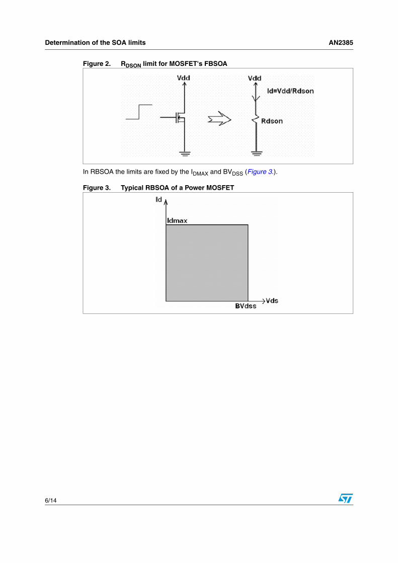
Another limit for FBSOA is established by RDSON of the device. In fact, when the device is in on state without loads connected to the component, all the voltage feed is applied on the drain-source terminals and, thus, the maximum drain current that can flow in the transistor is fixed by VDD and RDSON (Figure 2.).
Determination of the SOA limits AN2385
6/14
Figure 2. RDSON limit for MOSFET's FBSOA
In RBSOA the limits are fixed by the IDMAX and BVDSS (Figure 3.).
Figure 3. Typical RBSOA of a Power MOSFET
AN2385 Silicon limited drain current
7/14
2 Silicon limited drain current
Usually, in every Power MOSFET datasheet the drain current limit is fixed by the package limit. It depends on the kind, number and the size of the wires that connect the drain and the source pads to the respective package pins. However, another important parameter defined in the Power MOSFET datasheets is the Silicon Limited Drain Current. The Silicon Limited Drain Current is the maximum drain current that can flow in the device excluding the package limitation and considering as thermal impedance the junction to case thermal resistance value (RTHJC). Furthermore, the Silicon Limited Drain Current is typically calculated considering the device in "on state" with a case temperature equal to 25°C and supposing that it works at the maximum junction temperature. Considering this last operating condition, RDSON must be considered at the maximum junction temperature. It is around two times higher at the ambient temperature (25°C). In thermal equilibrium conditions, the following expression can be written as shown below:
Equation 1
PMAX is the maximum power that the device can dissipate at the maximum junction temperature. PMAX can be written as:
Equation 2
IDSL is the Silicon Limited Drain Current. IDSL can be written as:
Equation 3
Sometimes, in the Power MOSFET datasheets, the Silicon Limited Drain Current is shown at different case temperature conditions. In this case, the expression of IDSL becomes:
Equation 4
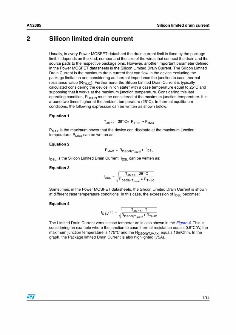
The Limited Drain Current versus case temperature is also shown in the Figure 4. This is considering an example where the junction to case thermal resistance equals 0.5°C/W, the maximum junction temperature is 175°C and the RDSON(TJMAX) equals 16mOhm. In the graph, the Package limited Drain Current is also highlighted (75A).
TJMAX 25° C RTHJC PMAX•=–
PMAX RDSON TJMAX( ) I2DSL•=
IDSLTJMAX 25° C–
RDSON TJMAX( ) RTHJC•-----------------------------------------------------------=
IDSL T( )TJMAX T–
RDSON TJMAX( ) RTHJC•-----------------------------------------------------------=

Silicon limited drain current AN2385
8/14
Figure 4. Silicon limited drain current vs case temperature
For Case Temperatures that are lower of around 110°C, the Package Limited Current is lower than the silicon one and thus, the device Limited Current is fixed at 75A. When the case temperature overcomes 110°C, the device Limited Current equals the Limited Silicon Current.

AN2385 Determination of the power dissipation and its derating factor
9/14
3 Determination of the power dissipation and its derating factor
The Power Dissipation value is the maximum power that the device can dissipate in continuous operating mode when the device works in "on state" and the thermal impedance is only due to RTHJC. The power dissipation depends on the case temperature. Typically, in Power MOSFET datasheets, it is reported at ambient temperature (25°C). In order to calculate the power dissipation value the consider RDSON value must be considered at the maximum junction temperature. It is possible to demonstrate that such value is around two times the values of RDSON at ambient temperature considering the data measured. Power Dissipation can be written as:
Equation 5
Furthermore, PD can be established for any other fixed operation case temperature considering that the guaranteed maximum junction temperature is 150°C or 175°C (see Figure 5.).
Figure 5. Power dissipation vs T
The Linear Derating Factor of Power Dissipation factor is defined as the angular coefficient of the line shown in Figure 5. It can be calculated as:
Equation 6
PD T 25° C=( )RDSON TJMAX IDSL( )( ) IDSL
2•TJMAX 25° C–
RTHJC---------------------------------==
∂PD
∂T----------
PD T 25° C=( )
TJMAX 25° C–--------------------------------- 1
RTHLJC--------------------==
Pulsed drain current (IDM) AN2385
10/14
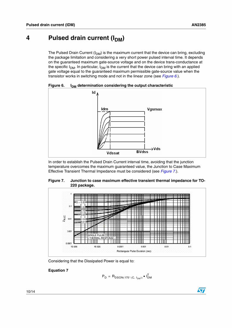
4 Pulsed drain current (IDM)
The Pulsed Drain Current (IDM) is the maximum current that the device can bring, excluding the package limitation and considering a very short power pulsed interval time. It depends on the guaranteed maximum gate-source voltage and on the device trans-conductance at the specific IDM. In particular, IDM is the current that the device can bring with an applied gate voltage equal to the guaranteed maximum permissible gate-source value when the transistor works in switching mode and not in the linear zone (see Figure 6.).
Figure 6. IDM determination considering the output characteristic
In order to establish the Pulsed Drain Current interval time, avoiding that the junction temperature overcomes the maximum guaranteed value, the Junction to Case Maximum Effective Transient Thermal Impedance must be considered (see Figure 7.).
Figure 7. Junction to case maximum effective transient thermal impedance for TO-220 package.
Considering that the Dissipated Power is equal to:
Equation 7
PD RDSON 175° C IDM,( )( ) IDM2•=

AN2385 Pulsed drain current (IDM)
11/14
where RDSON(175°C@IDM) is the on resistance of the device at the guaranteed maximum junction temperature and at the Pulsed Drain Current value, and that:
Equation 8
where ZTHJC is the junction to case thermal impedance at the specific operation conditions, the maximum acceptable ZTHJC value can be achieved as:
Equation 9
Thus, considering a specific Power Pulse with a fixed duty cycle, the maximum Rectangular Pulse Duration can be achieved.
As example, Figure 8. shows the determination of the maximum Rectangular Pulse Duration considering a Pulsed Drain Current equal to 600A, TJMAX of 175°C, case temperature of 25°C, duty cycle of 0.02 and RDSON(175°C, IDM) equal to 20mOhm. ZTHJC can be calculated as:
Equation 10
Figure 8. Determination of the maximum rectangular pulse duration
In this example, the maximum Rectangular Pulse Duration equals 30usec. For power pulse of higher duration the junction temperature overcomes 175°C and the device could fail.
It is important to highlight that the measured on resistance must be performed at the maximum junction temperature and also at the specific Pulsed Drain Current. In fact, increasing the drain current also RDSON increases and thus, of course, this effect must be taken into account.
PD ZTHJC• T TJMAX 25° C–=∆=
ZTHJCTJMAX 25° C–
RDSON175° C IDM
2,( )
------------------------------------------------=
ZTHJC175° C 25° C–
20 10 3– 600• 2•----------------------------------------------- 0.021
° CW-------•==

Conclusions AN2385
12/14
5 Conclusions
This technical article has explained what the Power Dissipation and its Linear Derating Factor, Silicon Limited Drain Current and Pulsed Drain Current (IDM) in MOSFET datasheets are and how they can be calculated. Furthermore, attention has also been placed on the definition of the MOSFETs SOA (FBSOA and RBSOA) and on the Junction to Case Maximum Effective Transient Thermal Impedance.

AN2385 Revision history
13/14
6 Revision history
Table 1. Revision history
Date Revision Changes
13-Jun-2006 1 Initial release

AN2385
14/14
Please Read Carefully:
Information in this document is provided solely in connection with ST products. STMicroelectronics NV and its subsidiaries (“ST”) reserve theright to make changes, corrections, modifications or improvements, to this document, and the products and services described herein at anytime, without notice.
All ST products are sold pursuant to ST’s terms and conditions of sale.
Purchasers are solely responsible for the choice, selection and use of the ST products and services described herein, and ST assumes noliability whatsoever relating to the choice, selection or use of the ST products and services described herein.
No license, express or implied, by estoppel or otherwise, to any intellectual property rights is granted under this document. If any part of thisdocument refers to any third party products or services it shall not be deemed a license grant by ST for the use of such third party productsor services, or any intellectual property contained therein or considered as a warranty covering the use in any manner whatsoever of suchthird party products or services or any intellectual property contained therein.
UNLESS OTHERWISE SET FORTH IN ST’S TERMS AND CONDITIONS OF SALE ST DISCLAIMS ANY EXPRESS OR IMPLIEDWARRANTY WITH RESPECT TO THE USE AND/OR SALE OF ST PRODUCTS INCLUDING WITHOUT LIMITATION IMPLIEDWARRANTIES OF MERCHANTABILITY, FITNESS FOR A PARTICULAR PURPOSE (AND THEIR EQUIVALENTS UNDER THE LAWSOF ANY JURISDICTION), OR INFRINGEMENT OF ANY PATENT, COPYRIGHT OR OTHER INTELLECTUAL PROPERTY RIGHT.
UNLESS EXPRESSLY APPROVED IN WRITING BY AN AUTHORIZE REPRESENTATIVE OF ST, ST PRODUCTS ARE NOT DESIGNED,AUTHORIZED OR WARRANTED FOR USE IN MILITARY, AIR CRAFT, SPACE, LIFE SAVING, OR LIFE SUSTAINING APPLICATIONS,NOR IN PRODUCTS OR SYSTEMS, WHERE FAILURE OR MALFUNCTION MAY RESULT IN PERSONAL INJURY, DEATH, ORSEVERE PROPERTY OR ENVIRONMENTAL DAMAGE.
Resale of ST products with provisions different from the statements and/or technical features set forth in this document shall immediately voidany warranty granted by ST for the ST product or service described herein and shall not create or extend in any manner whatsoever, anyliability of ST.
ST and the ST logo are trademarks or registered trademarks of ST in various countries.
Information in this document supersedes and replaces all information previously supplied.
The ST logo is a registered trademark of STMicroelectronics. All other names are the property of their respective owners.
© 2006 STMicroelectronics - All rights reserved
STMicroelectronics group of companies
Australia - Belgium - Brazil - Canada - China - Czech Republic - Finland - France - Germany - Hong Kong - India - Israel - Italy - Japan - Malaysia - Malta - Morocco - Singapore - Spain - Sweden - Switzerland - United Kingdom - United States of America
www.st.com