power distribution system: load modeling of a power...
TRANSCRIPT

`
TRABALHO DE CONCLUSÃO DE CURSO
POWER DISTRIBUTION SYSTEM:
LOAD MODELING OF A POWER DISTRIBUTION SYSTEM (PDS) FOR A MEDICAL IMAGING
PROCESSOR
Por,
Marina Gasparini de Barros
Vesna Resende Barros
Brasília, Dezembro de 2013

i
UNIVERSIDADE DE BRASILIA Faculdade de Tecnologia
Curso de Graduação em Engenharia Elétrica
TRABALHO DE CONCLUSÃO DE CURSO
POWER DISTRIBUTION SYSTEM:
LOAD MODELING OF A POWER DISTRIBUTION SYSTEM (PDS) FOR A MEDICAL IMAGING
PROCESSOR
POR,
Marina Gasparini de Barros
Vesna Resende Barros
Relatório submetido como requisito parcial para obtenção
do grau de Engenheiro Eletricista.
Banca Examinadora
Prof. Anésio de Leles Ferreira Filho, UnB/ ENE
(Orientador)
Prof. Pablo Eduarco Cuervo Franco, UnB/ENE
Prof. Jorge Cormane, UnB/ENE
Brasília, Dezembro de 2013

ii
FICHA CATALOGRÁFICA
GASPARINI DE BARROS, MARINA; RESENDE BARROS, VESNA
Power distribution system: Load modeling of a power distribution system (PDS) for a
medical imaging processor [Distrito Federal] 2013
xi, 60p., 297 mm (FT/UnB, Engenheiro, Eletricista, 2014). Trabalho de Graduação – Universidade de Brasília.Faculdade de Tecnologia.
1.Power Distribution System 2.Load Modeling
3.LTspice
I. Elétrica/FT/UnB
REFERÊNCIA BIBLIOGRÁFICA
BARROS, VR; GASPARINI, M (2013). Power distribution system: Load modeling of a power distribution system (PDS) for a medical imaging processor. Trabalho de Graduação em Engenharia Elétrica, Faculdade de Tecnologia, Universidade de Brasília, Brasília, DF, 60p.
CESSÃO DE DIREITOS
AUTOR: Marina Gasparini de Barros e Vesna Resende Barros.
POWER DISTRIBUTION SYSTEM: Load modeling of a power distribution system (PDS) for a medical imaging processor.
GRAU: Engenheiro ANO: 2014
É concedida à Universidade de Brasília permissão para reproduzir cópias deste Trabalho de
Graduação e para emprestar ou vender tais cópias somente para propósitos acadêmicos e
científicos. O autor reserva outros direitos de publicação e nenhuma parte desse Trabalho
de Graduação pode ser reproduzida sem autorização por escrito do autor.
____________________________ ____________________________
Marina Gasparini de Barros Vesna Resende Barros
SMAS Trecho 01 Lote C SQN 212 Bloco H Ap. 401 – Asa Norte
Bloco C Ap. 616 – Living Park Sul 70864-080 Brasília – DF – Brasil
71218-010 Guará – DF – Brasil

iii
AGRADECIMENTOS
Dedico esta obra aos meus pais, Fátima e Paulo, por todo o suporte, amor e incentivo ao
longo de todos esses anos. Sem o grande esforço de ambos, provavelmente não haveria
chegado até aqui.
Ao meu grande companheiro e amor, Gilberto, pelo seu carinho, companheirismo e
dedicação sempre presentes, principalmente durante os meses que passamos longe para
que este trabalho de fim de curso fosse concretizado.
À minha amiga e companheira, Vesna, por todo apoio e dedicação para a realização
deste trabalho.
Obrigada a todos. Amo vocês.
Marina Gasparini.
Aos meus amados pais, Sirleny e Lucas, por todo carinho, amor, dedicação e apoio
doados a mim em cada passo da minha vida.
Aos eternos amigos, Cecília, Danielli, Marcelo e Vanessa, por darem significado as
palavras companheirismo, cumplicidade e lealdade.
À minha companheira de projeto, Marina, pela grande amizade e por estar presente ao
meu lado durante essa caminhada.
A todos os colegas de curso.
Vesna Resende Barros

iv
ABSTRACT
Philips Healthcare is researching and developing a new power distribution architecture that is
intended to power different medical equipment, such as computed tomography, radiography,
ultrasound and interventional X-ray equipment. The objective of this new architecture is to
improve the safety in using these medical devices during operations, but it is further intended
to power other non-medical devices as well.
Some parts of the new architecture, like the power source and the Power Distribution System
(PDS) have already been designed by Philips and former students. However, the load model
that is connected to the system still needs to be tested and validated in order to have the
whole architecture completed.
Therefore, this report contains the results obtained after six months studying the loads
characteristics of the system. A computational model was designed in LTspice IV software to
predict the behavior of different loads when connected to the PDS. In the model, the load
was represented by electronic components described by values that change over time.
These values are set by the user with the purpose of analyzing the variations of voltage and
currents during the load operation time, and they were carefully chosen in order to provide
the results most similar to real life.
After simulating, measurements with real loads in the X-Ray laboratory were analyzed and
compared with the previous computational results. A validation tool was used to verify the
closeness of the simulations to the practical measurements. In preparing and designing the
models, an accuracy of 10% between the models and the practical results is expected.
Keywords: Power Distribution System; Load Modeling; LTspice

v
CONTENTS
Assignment Description ................................................................ 12
1. Introduction ............................................................................. 15
1.1 Electric Power Distribution System ..................................................................... 16
1.2 Inrush Current ..................................................................................................... 17
2. Magnetic Components ............................................................ 20
3. Load Model Building ............................................................... 26
1.3 Software Simulation ............................................................................................ 26
1.4 Data Interpolation ............................................................................................... 32
4. Practical Analysis ................................................................... 35
5. Results and Discussion .......................................................... 43
6. Conclusions ............................................................................ 46
Appendix A – Load Modeling ........................................................ 48
Appendix B – Load Types ............................................................. 51
Appendix C – Computational Model ............................................. 57
Appendix D – Lab Measurements ................................................. 63
References ..................................................................................... 73

vi
LIST OF FIGURES
Figure 1: Power Flow Diagram ........................................................................................ 12
Figure 2: Power Distribution System Schematic .............................................................. 14
Figure 3: Overview of Electrical Distribution System ....................................................... 16
Figure 4: Three phase AC waveform .............................................................................. 17
Figure 5: Current waveform when the device is powered up ........................................... 18
Figure 6: The electric circuit of an ideal transformer ........................................................ 20
Figure 7: Equivalent electric circuit of saturable core model ............................................ 21
Figure 8: Complete transformer model ............................................................................ 22
Figure 9: The result when simulating the complete transformer model ............................ 23
Figure 10: Results obtained when the amplitude of the input voltage source was varied
and set as (a) 2 volts, (b) 5 volts and (c) 10 volts.................................................................. 24
Figure 11: Hysteresis curve and output voltages and current obtained with the source
switched on at (a) 0° and (b) 90° .......................................................................................... 25
Figure 12: Single phase load described as a mathematical function ............................... 27
Figure 13: Voltage at the source and current at the load ................................................. 28
Figure 14: DCPS VWCB receiver modules (B-Cabinet) .................................................. 28
Figure 15: DCPS VWCB receiver modules (B-Cabinet) .................................................. 28
Figure 16: CRCB continuous (M-Cabinet) ....................................................................... 29
Figure 17: SIB (M-cabinet) .............................................................................................. 29
Figure 18: Host PC (M-Cabinet) ...................................................................................... 29
Figure 19: Tube Cooler F (M-Cabinet) ............................................................................ 30
Figure 20: Circuit model (CRCB monitor) ........................................................................ 31
Figure 21: Simulation of CRCB monitor circuit model ...................................................... 31
Figure 22: Linear interpolation between two points. ........................................................ 32
Figure 23: Validation CRCB monitor model ..................................................................... 33
Figure 24: Monitor's waveforms when the power is switched on at 0° (on the left) and at
90° (on the right) .................................................................................................................. 35

vii
Figure 25: DCPS's waveforms when the power is switched on at 0° (on the left) and at
90° (on the right) .................................................................................................................. 35
Figure 26: Current x Phase for the monitor ..................................................................... 36
Figure 27: Current x Phase for the DCPS ....................................................................... 36
Figure 28: Monitor circuit................................................................................................. 37
Figure 29: DCPS circuit .................................................................................................. 37
Figure 30: Validation for the monitor at 0° ....................................................................... 38
Figure 31: Validation for the monitor at 90° ..................................................................... 38
Figure 32: Validation for the DCPS at 0° ......................................................................... 39
Figure 33: Validation for the DCPS at 90° ....................................................................... 39
Figure 34: Error for the monitor in phase 0°. ................................................................... 40
Figure 35: Error for the monitor in phase 90°. ................................................................. 40
Figure 36: Error for the DCPS in phase 0°. ..................................................................... 41
Figure 37: Error for the DCPS in phase 90°. ................................................................... 41
Figure 38: A single phase source with a variable resistor ................................................ 48
Figure 39: Output voltage and current on the resistor ..................................................... 48
Figure 40: A single phase source with a varistor ............................................................. 49
Figure 41: Output voltage and current on the varistor ..................................................... 50
Figure 42: 1st DCPS VWCB receiver modules (B-Cabinet) .............................................. 51
Figure 43: 2nd Optical DL DVI splitter (B-Cabinet) ........................................................... 51
Figure 44: Dual Link splitter (B-Cabinet) ......................................................................... 51
Figure 45: 2nd DCPS VWCB receiver modules (B-Cabinet) ............................................. 52
Figure 46: 3rd DCPS VWCB receiver modules (B-Cabinet) ............................................. 52
Figure 47: 2nd MCS monitors (WME 1.8) (M-Cabinet) ..................................................... 52
Figure 48: CRCB continuous (M-Cabinet) ....................................................................... 53
Figure 49: CRCB switched (M-cabinet) ........................................................................... 53
Figure 50: 16x16 DVI matrix switch (B-cabinet) .............................................................. 53
Figure 51: SIB (M-cabinet) .............................................................................................. 54
Figure 52: Host PC (M-Cabinet) ...................................................................................... 54

viii
Figure 53: IP PC F (M-Cabinet) ....................................................................................... 54
Figure 54: IP PC L (M-Cabinet) ....................................................................................... 55
Figure 55: Flexvision Dell PC (B-cabinet) ........................................................................ 55
Figure 56: Tube Cooler F (M-Cabinet) ............................................................................ 56
Figure 57: Tube Cooler L (M-Cabinet) ............................................................................. 56
Figure 58: 1st DCPS VWCB receiver modules ................................................................. 57
Figure 59: 2nd Optical DL DVI splitter ............................................................................. 57
Figure 60: Dual Link Splitter ............................................................................................ 58
Figure 61: 2nd DCPS VWCB receiver modules. ............................................................... 58
Figure 62: 3nd DCPS VWCB receiver modules ................................................................ 58
Figure 63: MCS Monitor .................................................................................................. 59
Figure 64: CRCB Monitor ................................................................................................ 59
Figure 65: 16x16 DVI matrix switch ................................................................................. 60
Figure 66: SIB ................................................................................................................. 60
Figure 67: Host PC ......................................................................................................... 60
Figure 68: IP PC F .......................................................................................................... 61
Figure 69: IP PC L .......................................................................................................... 61
Figure 70: Flexvision Dell PC .......................................................................................... 61
Figure 71: Tube Cooler F ................................................................................................ 62
Figure 72: Tube Cooler L ................................................................................................ 62
Figure 73: Monitor (power switched in phase 𝟎°) ............................................................ 63
Figure 74: Monitor (power switched in phase 𝟑𝟎°) .......................................................... 63
Figure 75: Monitor (power switched in phase 𝟔𝟎°) .......................................................... 63
Figure 76: Monitor (power switched in phase 𝟗𝟎°) .......................................................... 64
Figure 77: Power Supply (power switched in phase 𝟎°) .................................................. 64
Figure 78: Power Supply (power switched in phase 𝟑𝟎°) ................................................ 64
Figure 79: Power Supply (power switched in phase 𝟔𝟎°) ................................................ 65
Figure 80: Power Supply (power switched in phase 𝟗𝟎°) ................................................ 65
ix
Figure 81: Monitor (power switched in phase −𝟑𝟎°) ........................................................ 65
Figure 82: Monitor (power switched in phase −𝟔𝟎°) ........................................................ 66
Figure 83: Monitor (power switched in phase −𝟗𝟎°) ........................................................ 66
Figure 84: Power Supply (power switched in phase −𝟑𝟎°) .............................................. 66
Figure 85: Power Supply (power switched in phase −𝟔𝟎°) .............................................. 67
Figure 86: Power Supply (power switched in phase −𝟗𝟎°) .............................................. 67
Figure 87: Monitor Phase 𝟎° ........................................................................................... 67
Figure 88: Monitor Phase 𝟑𝟎° ......................................................................................... 68
Figure 89: Monitor Phase 𝟔𝟎° ......................................................................................... 68
Figure 90: Monitor Phase 𝟗𝟎° ......................................................................................... 68
Figure 91: Monitor Phase −𝟑𝟎° ....................................................................................... 69
Figure 92: Monitor Phase −𝟔𝟎° ....................................................................................... 69
Figure 93: Monitor Phase −𝟗𝟎° ....................................................................................... 69
Figure 94: DCPS Phase 𝟎° ............................................................................................. 70
Figure 95: DCPS Phase 𝟑𝟎° ........................................................................................... 70
Figure 96: DCPS Phase 𝟔𝟎° ........................................................................................... 70
Figure 97: DCPS Phase 𝟗𝟎° ........................................................................................... 71
Figure 98: DCPS Phase −𝟑𝟎°......................................................................................... 71
Figure 99: DCPS Phase −𝟔𝟎°......................................................................................... 71
Figure 100: DCPS Phase −𝟗𝟎° ....................................................................................... 72

x
LIST OF TABLES
Table 1: Loads Errors....................................................................................................... 43
Table 2: Monitor and DCPS Errors................................................................................... 45

xi
LIST OF ABBREVIATONS
AC Alternate Current
DC Direct Current
DCPS Direct Current Power Supply
DL DVI Dual-Link Digital Visual Interface
LSO Load Side Option
MCS Monitor and Control Software
MMF Magnetomotive Force
PCM Power Control Manager
PDM Power Distribution Manager
PDS Power Distribution System
PE Protective Earth
PPB Pulse Power Bus

12
ASSIGNMENT DESCRIPTION
Philips Healthcare is a company responsible to develop and market solutions that promote
wellness for people around the globe. The Healthcare sector’s vision is to improve the quality
of patients’ lives by simplifying the delivery of healthcare, improving clinical outcomes and
reducing healthcare system costs around the world [1]. The Power Distribution System
(PDS) project is executed within the Research and Development department of the business
unit interventional X-Ray. This department is specialized in the development imaging
equipment for interventional imaging, treatment and clinical research.
This study is about a new power distribution architecture that is intended to be scalable
and applicable for powering medical facilities with imaging equipment. Part of the system is
already finished, but there is still an amount of loads that needs to be tested. Therefore, the
aim of this assignment will be focused on the load models and their parameterization. It will
involve application and verification activities for the created models (in LTspice software),
executing the models in order to yield predictions about the outcome of real life verification
measurements. After data collection and analysis, it will be necessary to feed the information
back into the model, in order to have improvement in the accuracy and, if applicable, apply
the necessary corrections into the models.
The Spice models that were developed are based on the flow of power within the power
system. The electrical power that comes through the lines distributions flows into the hospital
mains over the Power Distribution System (PDS). The PDS is an architecture that has been
concept by Philips Healthcare after years of research. This architecture consists of a power
distribution platform for medical purposes composed by building blocks model interfaces [3].
The schematic, shown in Figure 1, illustrates the flow of power from the hospital mains until
the load.
SOURCE
(Hospital Mains)PDS
LOAD(Medical Imaging
Processors, monitors…)
Figure 1: Power Flow Diagram

13
Considering the PDS structure, it can be divided in three main parts.
1) Power Control Manager (PCM) Domain: The central domain that converts, switches,
distributes, buffers and monitors the power. The distribution constitutes in partitioning
in to power bus (PDS.IF.PB) and pulse-power-bus (PDS.IF.PPB) root terminals. It
converts a 400/230V Wye configuration into the power-bus and 380-480V. It switches
on/off the output power of the PB and PPB roots. By buffering, it storages the energy in
batteries and use the energy to continue providing output power in case of lost power
in the source.
2) Power Distribution Manager (PDM) Domain: The PDM is a slave of the PCM
master controller. It converts a three phase in to a single-phase and phase
association section. It taps the switching of single phase loads and splits off into
multiple and identical tap channels. It stores the energy in batteries in order to provide
output power in case of lost power in the source.
3) Load Side Option (LSO) Domain: This domain is responsible to distributes, converts and
conditions the power in physical proximity of the load. All functions are intended to
adapt the PDM.
The power will flow through the hospital mains to the PDM. After entering the PDM, the
power will be split into two paths. One path is the 3 Phase Pulse Power Bus (PPB), which will
distribute the power to the Medical Imaging Processor. The other path is the 3 Phase Power
Bus with UPS (PB), responsible for the power distribution for the single phase tap switching
units, which can be paralleled towards multiple single phase loads. In this path, there may
also be a connection from the tap switch to a DC load via a Load Side Option (LSO). The
PDS has the main purpose of mitigate distortions deriving by the power source. The
schematic of this system is illustrated by Figure 2.

14
SOURCE(Hospital Mains)
PDS PCM Domain
PDM Domain
TAP SWITCHES
Medical Imaging Processor
Single Phase Load
Single Phase Load
Single Phase Load
DC load
PPB
LSO
PB
Figure 2: Power Distribution System Schematic
Due to limitations of time, it was only possible to develop a model for the AC loads. This
way, further studies can be done with the DC and the three-phase delta loads in order to
complete the architecture. This project will describe the different load models simulated in
LTspice and the measurements with real loads in the X-Ray laboratory. At the end, the
results will be validated to see how close the models are from the real loads.

15
1. INTRODUCTION
The PDS is a big architecture whose performance is difficult and complex to test. The
best way to verify the system’s performance is through simulation, once it enables to check
the results beforehand and helps to get information of the system’s behavior without testing it
in real life. However, the process of designing this architecture, as well as simulating the
loads connected to it, involves a deep understanding of the load’s electronic circuit that
causes a certain behavior when the voltage is switched on. Understanding this behavior is
the goal of this study because we are mostly interested in the current that is generated when
the device is first turned on. These currents, usually called inrush currents, have a huge
influence on the device’s operation life since they exceed the steady-state current value.
The models designed in LTspice software were based in the power flow diagram that was
shown in Figure 1. It means that the electrical circuits’ models present, in a simple way, the
switch mode power supply, the PDS and the load. The power supply was designed in a way
that it can be switched on at any time, according to the configurations set by the user. The
phase of the voltage waveform can also be changed in order to understand its influence on
the inrush current peak value. The variable parameters that describe the circuits are set in
specific values in order to simulate specific loads. Each load has a fixed value for each
parameter, and these values were carefully tested to approach the result most similar to the
lab result for that load.
This report contains the activities that were done, the obstacles encountered, the
solutions defined and the results that were found. In this first chapter, a brief introduction to
the power distribution system is given for a clearer understanding of the entire process.
Moreover, there will be a section explaining the inrush current, since it’s the main
phenomenon that we are interested in. Explanations about how the models were created are
found in chapter 2, Load Building Model, and the laboratory measurements and analysis can
be found in chapter 3, Practical Analysis. The results and discussion are in chapter 4 and
finally, the conclusions are written on chapter 5. A lot of practical results were left outside the
main part of the report, but they can be found on the appendices.
Finally, it’s important to emphasize that all of the computational models created were
based on the current and voltage waveforms contained on the characterization report of
2013, with the exception of the DCPS and the monitor, that were based on our own
measurements in the lab. All of the measurements and the resulting graphs can be found on
the Appendices B and C.

16
1.1 Electric Power Distribution System
The three-phase electric power is a method of alternating-
current power generation, transmission, and distribution. Figure 3 shows this polyphase
system, which is the most common method used by electrical grids worldwide to transfer
power. A three-phase system is usually more economical than an equivalent single-
phase or two-phase system because it uses less conductor material to transmit electrical
power [4].
Figure 3: Overview of Electrical Distribution System
At the power station, an electrical generator converts mechanical power into a set of
three AC electric currents, one from each winding of the generator. The windings are
arranged such that the currents vary sinusoidally at the same frequency (50 Hz in the
Netherlands) but reach their instantaneous peak values at one third of a cycle from each
other. Taking one current as the reference, the other two currents are delayed in time by one
third and two thirds of one cycle of the electric current (Figure 4). This delay between phases
has the effect of giving constant power transfer over each cycle and also makes it possible to
produce a rotating magnetic field in an electric motor.

17
Figure 4: Three phase AC waveform
Generating step up transformers change the voltage from generators to a higher level
suitable for transmission in order to avoid losses during transmissions. These voltages are
extremely high, producing low currents and therefore less power loss.
After transmission, the step down transformer reduces the primary voltage to a level
where it can be used by the end costumers, which can be, for instance, an industry, the
hospital mains or houses. In the latter, it is a three-phase to single phase conversion and it’s
referred to as a delta-to-wye conversion.
All of the electrical power that comes out from this distribution system and enters the
hospital mains flows into the PDS, as shown in the schematic in Figure 1. At the end, the
electrical power that is out of the PDS will be connected to different medical equipment which
will be defined as the load for this assignment.
1.2 Inrush Current
In order to power these medical appliances, one should take into account the safety
requirements and the maximum allowable currents that a specific device can tolerate without
any damages. The maximum and instantaneous input current drawn by an electrical device
when power is first applied is called inrush current and it can affect electrical components
inside a circuit and failure within the equipment itself.
The inrush current is greater than the nominal operating current of the equipment and its
value varies according to the equipment in question and the state of operation. It can range
from 5 to 100 times greater the normal full load current.
The figure below shows an example of an inrush current from one of the loads tested in
the laboratory, the DCPS VWCB receiver module.

18
Figure 5: Current waveform when the device is powered up
When the power is turned on, current begins to flow, and the initial current flow reaches
the peak current value that is larger than the steady-state current value. Following this, the
current value gradually decreases until it stabilizes at the steady-state current. The part
during which a large current flows before reaching the steady-state current is the inrush
current. If the size of the inrush current exceeds that allowed by the part in use, depending
on the magnitude of the inrush current (difference between the peak current value and the
steady-state current value) and length of its duration (the length of time until the peak current
value converges with the steady-state current value, hereafter called the pulse width), the
part used in the circuit may overheat, potentially causing the electrical device to malfunction
or break down.
The reasons why this inrush current occurs vary according to each device. In general, in
equipment with large-capacity smooth capacitors or decoupling capacitors, when the power
is first turned on, a large current flow to charge those capacitors – a necessity when first
powering up the equipment. Another reason is that immediately after the power is turned on,
the filament and other parts have low resistance, so large current flows. As they begin to
generate heat and warm up, the resistance increases and the current drops to the steady-
state current.
If the load is connected to an AC powered source, the maximum inrush is dependent on
the point on the AC waveform at the time it is switched on [5]. As it will be seen later on this
report, the load may be connected when the mains waveform passes through zero or at the
very peak of the voltage waveform. It can also be connected between the two points, but
mostly it will be somewhere between the two extremes, and the cycle could be positive or
negative.

19
Transformers and other inductive circuits behave in a manner that is not intuitive. In a
transformer, for example, the greatest magnitude of inrush current occurs at the zero
crossing of the terminal voltage, whereas the lowest magnitude occurs when the power is
connected at the peak of the AC voltage waveform. This is because at the zero crossing the
flux saturates the core and a high amplitude inrush current appears, since the inductance of
the magnetic core is very small in that region. Therefore, the peak current is only limited by
the circuit resistance and the current is determined by Ohm’s law.
Since it is not possible to choose when power is applied, any provision for inrush current
must assume the highest possible value.

20
2. MAGNETIC COMPONENTS
Due to the presence of the magnetic components in many power electronic equipment of
the PDS, a certain time of this internship was dedicated to study more deeply this kind of
devices. Although LTSpice offers a few magnetic components built into it, the most reliable
way to create these models is to base them on the actual physical structure of the
component. It means, for example, that a transformer won’t be represented by a coupled
inductor model, but by a circuit that mimics the behavior of the transformer. Therefore, the
physical structure of the device needs to be translated into an equivalent electric circuit [6].
To make a transformer model that more closely represents the physical processes, it is
necessary to construct an ideal transformer and model the magnetizing and leakage
inductances separately. The SPICE equivalent circuit for an ideal transformer is shown in
Figure 6, and it implements the following equations:
V1*ratio = V2
I1 = I2*ratio
Figure 6: The electric circuit of an ideal transformer
In the circuit above, the voltage-controlled voltage source is set with the turns ratio from
the windings and the resistances Rp and Rs are used to prevent singularities in the matrix
used by SPICE to calculate the voltages and currents.
The nonlinear characteristics of the transformer are performed by another electric circuit
shown in Figure 7. It represents a single coil wound around a magnetic core, which is
consisted of many magnetic domains made up of magnetic dipoles. These domains set up a
magnetic flux that adds to the flux that is set up by the magnetizing current. In the presence
of an applied field, the domains rotate until they are all in alignment with the field and the
core saturates.

21
Figure 7: Equivalent electric circuit of saturable core model
Modeling the nonlinearities of a transformer is more easily accomplished by adding
nonlinear elements to the model. In this case, the diodes are responsible for causing the
expected behavior of the transformer, making it possible to plot the B-H loop hysteresis
curve. The capacitor Cb is described by an initial condition that allows the core to have an
initial flux, whereas resistors Rb and Rs are responsible for the inductance in the high-
permeability region and the saturated region, respectively. The voltage sources Vn and Vm
represent the saturation flux and Rx simulates the core losses, which increase linearly with
frequency.
The characteristics of the core are determined via the specification of a few parameters:
Flux capacity in volt-seconds (VSEC)
Initial flux capacity in volt-seconds (IVSEC)
Magnetizing inductance in henries (LMAG)
Saturation inductance in henries (LSAT)
Eddy current critical frequency in hertz (FEDDY)
The values attributed to each parameter were calculated in order to find compatible
results with magnetic components’ behavior. These values can be seen as a SPICE directive
on LTSpice schematic on Figure 7.
The saturable core is added to the model of the ideal transformer to create a complete
transformer model. It is a piece of magnetic material with a high permeability used to confine
and guide magnetic fields in electrical and magnetic devices such as transformers, electric
motors, inductors and magnetic assemblies. The high permeability, relative to the
surrounding air, causes the magnetic field lines to be concentrated in the core material. The
magnetic field is often created by a coil of wire around the core that carries a current. The
presence of the core can increase the magnetic field of a coil by a factor of several thousand
22
over what it would be without the core. The use of a magnetic core can enormously
concentrate the strength and increase the effect of magnetic fields produced by electric
currents and permanent magnets.
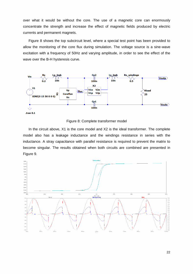
Figure 8 shows the top subcircuit level, where a special test point has been provided to
allow the monitoring of the core flux during simulation. The voltage source is a sine-wave
excitation with a frequency of 50Hz and varying amplitude, in order to see the effect of the
wave over the B-H hysteresis curve.
Figure 8: Complete transformer model
In the circuit above, X1 is the core model and X2 is the ideal transformer. The complete
model also has a leakage inductance and the windings resistance in series with the
inductance. A stray capacitance with parallel resistance is required to prevent the matrix to
become singular. The results obtained when both circuits are combined are presented in
Figure 9.

23
Figure 9: The result when simulating the complete transformer model
In the first graph, the light blue curve represents the magnetic intensity field and magnetic
flux density plot. When the magnetic field through the core changes, the magnetization of the
core material changes by expansion and contraction of the tiny magnetic domains it is
composed of, due to movement of the domain walls. This process causes losses, because
the domain walls get snagged on defects in the crystal structure and then snap past them,
dissipating energy as heat. This is called hysteresis loss. It can be seen in the graph of the B
field versus the H field for the material, which has the form of a closed loop. The amount of
energy lost in the material in one cycle of the applied field is proportional to the area inside
the hysteresis loop.
The second graph shows the input voltage (in gray), output voltage (blue) and the current
through the core (red). When the core reaches the saturation, the losses become larger,
affecting directly the output voltage and deforming characteristically the sinus waveform. The
distortion of the sine wave is more perceptible in the zero-crossing points of the voltage
source, where the derivative 𝑑𝑉(𝑡)
𝑑𝑡 is maxim. In these points, the core saturates easily,
stressing the transformer and causing dissipation of energy in the core, and not on the load.
If we now change the amplitude of the source the dependence of the saturation on the
voltage becomes clearer. Increasing the voltage amplitude causes an increase in the
magnetomotive force (MMF), which in turn causes a larger magnetic flux and the core
saturates easier. To visually represent this relation, Figure 10 shows three examples where
the amplitude of the input voltage was varied.
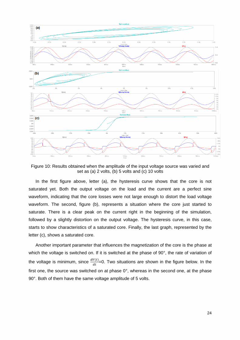
24
Figure 10: Results obtained when the amplitude of the input voltage source was varied and set as (a) 2 volts, (b) 5 volts and (c) 10 volts
In the first figure above, letter (a), the hysteresis curve shows that the core is not
saturated yet. Both the output voltage on the load and the current are a perfect sine
waveform, indicating that the core losses were not large enough to distort the load voltage
waveform. The second, figure (b), represents a situation where the core just started to
saturate. There is a clear peak on the current right in the beginning of the simulation,
followed by a slightly distortion on the output voltage. The hysteresis curve, in this case,
starts to show characteristics of a saturated core. Finally, the last graph, represented by the
letter (c), shows a saturated core.
Another important parameter that influences the magnetization of the core is the phase at
which the voltage is switched on. If it is switched at the phase of 90°, the rate of variation of
the voltage is minimum, since 𝑑𝑉(𝑡)
𝑑𝑡=0. Two situations are shown in the figure below. In the
first one, the source was switched on at phase 0°, whereas in the second one, at the phase
90°. Both of them have the same voltage amplitude of 5 volts.

25
Figure 11: Hysteresis curve and output voltages and current obtained with the source switched on at (a) 0° and (b) 90°
As seen before in Figure 10b, the first graph shows a situation where the core is
saturated. The inrush current present in the graph is due to the power that was first applied
with the AC source at the zero-crossing point. This peak is not present in the second graph,
where the source was switched on at 90°. In this case, the transformer is not saturated, even
connected to a source with the same amplitude. The hysteresis curve has an interesting
behavior: its initial magnetizing curve is a horizontal line. It means that there is an increase in
the magnetic flux, even with no increase in the intensity of the magnetic field.
Avoiding high magnitudes of inrush current is extremely important in the protection of
electronic devices. This is the reason why control switching is so important: the inrush
current can be minimized when powering a transformer at the maximum peak voltage (90°).
Although the models built so far properly represent the nonlinear permeability and the
hysteresis, there was still one model left that was not simulated due to time limitations. This
model represents low-frequency hysteresis in transformers, and can be studied by the next
team that will take this project.

26
3. LOAD MODEL BUILDING
Appropriately modeling load characteristics is important for power distribution analysis, in
particular for presuming the behavior of the system when the load is connected to it. It is not
an easy task, since the sensitivity of the system behavior to changes in load response must
be clearly understood.
In order to improve the process and accuracy of the PDS and to be able to make rational
and economical decisions, a verification tool is needed to facilitate and to reduce the costs of
testing. LTspice was the software used to acquire the necessary characteristics and
parameters with respect to the various kinds of loads in the power system, such as the PCs,
the monitors and the X-ray machines.
The result of the simulations developed in LTspice led to a better understanding of the
load dynamics and therefore to an improved load representation, making it possible to
decrease uncertainty margins, resulting in a positive impact on the reliability of the system
operation.
1.3 Software Simulation
LTspice IV is a high performance SPICE simulator, schematic capture and waveform
viewer with models for easing the simulation of switching regulators. The benefit of using a
simulator is that it provides us a guideline for expected results in the laboratory. It is also
useful for purposes of comparison between what was observed in the software and what was
seen in the practical measurements. This way, it’s possible to verify if models created are
following real life expectations.
The modeling of the load has started with some simple resistive, RL, RC, and RLC single
phase loads simulations, providing not only the circuits behavior analyses, but also an easy
way to improve the skills with the software`s tools. After this initial contact with LTspice, the
main focus on the load design was to turn the computational model as close to a real load
behavior as it could.
In the hospital, more specifically in an X-Ray room, three phase (e.g. the X-Ray
generator) and single phase (e.g. monitors) loads are connected to the power distribution
system. Although the simulation of the original circuits of this kind of load provides more
reliable results, the time to simulate them becomes inappropriate. Therefore, it’s necessary
to look for a solution that provides good results in a short period of time.

27
In order to visualize one of the most expressive behaviors of the load, the inrush current,
a few techniques to vary the impedance of the computational load model were applied. In the
beginning, a single load was designed using first a variable resistor and then using a varistor.
In both cases, the results were not so meaningful and it will be discussed on the Appendix A
– Load Modeling.
The second step taken was to impose a mathematical function that could describe the
inrush current in a resistive component. Thus, a resistor was described as growing
exponential damped over time, as illustrated in Figure 12.
Figure 12: Single phase load described as a mathematical function
The schematic represented by Figure 12 illustrates in a simple way a single phase load
supplied by an AC voltage source, connected to a power distribution unit (represented by the
resistor R1). The resistors R2 and R3 represent, respectively, the neutral and the Protective
Earth (P.E). The high resistance value of R5 ensures that no current runs through the P.E.
Through LTspice simulation, the voltage at the source and the current at the load are
presented in Figure 13.

28
Figure 13: Voltage at the source and current at the load
In the PDS, the measurements can be done in three different cabinets: B, M and R. For
each one of these cabinets, different types of loads have been tested, having their current
waveform displayed in the scopemeter. Once the representation of the resistive load as a
function of time was successful, the next step taken was to establish for the B and M
cabinets (for a matter of time, only these two were analyzed) types of loads that have similar
behavior in order to parameterize them. The loads have been allocated in six groups that
hold similar characteristics, providing an easy way of modeling and parameterization.
Through the loads characterization and with LTspice support, each type of load was
described as function of time supplied by a switch mode power supply hooked up through
resistors that represent the losses in the transmission line.
One example of the inrush current for each type is shown below and the complete list of
load type can be found in the Appendix B - Load Types.
Type A
Figure 14: DCPS VWCB receiver modules (B-Cabinet)
Type B
Figure 15: DCPS VWCB receiver modules (B-Cabinet)

29
Type C
Figure 16: CRCB continuous (M-Cabinet)
Type D
Figure 17: SIB (M-cabinet)
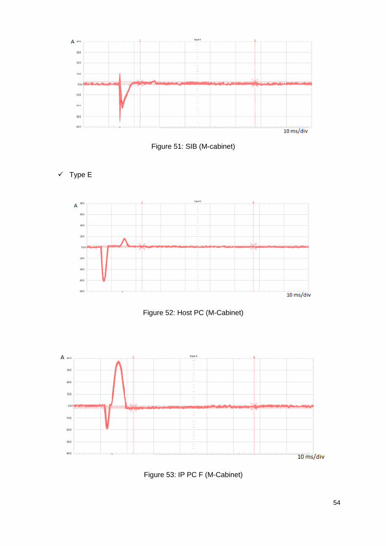
Type E
Figure 18: Host PC (M-Cabinet)

30
Type F
Figure 19: Tube Cooler F (M-Cabinet)
It is remarkable that loads of types A to E present a similar inrush behavior – all of them
present a huge first peak that is sometimes followed by other smaller peaks before it reaches
the steady-state current. This is due to the presence of the DC Power Supply (DCPS) in
these circuits. Loads of type F, on the other hand, have an inrush current behavior that is
similar to a sinusoidal waveform, presenting some shifting, that persists from the beginning to
the end. This characteristic is based on that the tube cooler (a type F load) is composed by
some inductive components (e.g. the fan and the motor) that may shift or distort the sine
wave.
The difference observed between the current waveforms of loads from type A to E is
caused by the many different components inside the DCPS. In a typical power supply, the
AC input voltage deriving of the mains power is stepped down to a desired level using a
transformer. When it is already stepped down, AC voltage is connected to a rectifier diode
that converts the AC voltage in to a pulsating DC. This conversion is based on the principle
that a diode acts as a conductor with a very low resistance when forward biased, and acts as
an insulator with a very high resistance when reverse biased. An electrolytic capacitor used
for storing energy is usually connected across the DC output of the rectifier diode, providing
an extra degree of smoothing the output waveform.
In general, all types of loads are represented by the same electrical circuit. What changes
from group to group is the mathematical function that describes the resistor in the circuit,
which represents the load. This way, it is possible to use the same mathematical function to
simulate different loads that belong to a particular group, but the user must change the
function’s parameters when changing the load within that group.
31
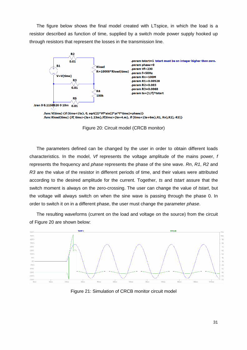
The figure below shows the final model created with LTspice, in which the load is a
resistor described as function of time, supplied by a switch mode power supply hooked up
through resistors that represent the losses in the transmission line.
Figure 20: Circuit model (CRCB monitor)
The parameters defined can be changed by the user in order to obtain different loads
characteristics. In the model, Vf represents the voltage amplitude of the mains power, f
represents the frequency and phase represents the phase of the sine wave. Rn, R1, R2 and
R3 are the value of the resistor in different periods of time, and their values were attributed
according to the desired amplitude for the current. Together, ts and tstart assure that the
switch moment is always on the zero-crossing. The user can change the value of tstart, but
the voltage will always switch on when the sine wave is passing through the phase 0. In
order to switch it on in a different phase, the user must change the parameter phase.
The resulting waveforms (current on the load and voltage on the source) from the circuit
of Figure 20 are shown below:
Figure 21: Simulation of CRCB monitor circuit model
32
It’s clear that the variation of the resistor values causes the changes in the current
waveform. The nominal value, Rn, is responsible for the steady-state current value and it
was determined based on the characterization report of 2013. R1, R2 and R3 were first
determined by Ohm’s law and had their values increased or decreased until the right
amplitude of inrush current was found. The pulse width was first measured in the Flukeview
software and then written on the resistor function. Together, the parameters describe the
function that simulates the behavior of the real load.
1.4 Data Interpolation
After the circuit simulation, the data from FlukeView (showing the original waveform) and
LTspice were imported to an Excel file in order to validate the models through the error
calculation between these two waveforms. However, not only the number of sampling points
was different, but also the simulation time step of both softwares was not the same, making it
difficult to calculate the error point by point. So in order to verify the accuracy of the model,
an interpolation in the model`s data became necessary.
First, the interpolation was done with the help of LTsputil, an utility software for LTspice
which allows the user to change the numbers of sampling points and the simulation time step
of the original LTspice file. The software automatically generates a new LTspice raw data file
with the new parameters set by the user. In this case, the interpolation is based on the
Polynomial Interpolation method, which from an amount of given points, finds a polynomial
equation that fits exactly these points. However, this kind of interpolation became
undesirable, since the waveforms got really distorted after the interpolation, losing the
similarity with the real load behavior.
The other interpolation method applied to the models was the linear interpolation, using
Excel as a tool. A linear interpolation is a simple method that assumes a straight line (linear)
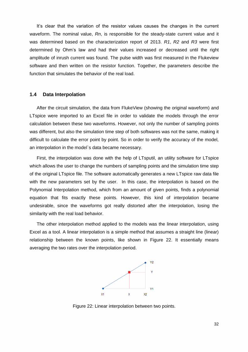
relationship between the known points, like shown in Figure 22. It essentially means
averaging the two rates over the interpolation period.
Figure 22: Linear interpolation between two points.

33
The diagram above shows two points (blue points connected by a blue line) with
coordinates (X1, Y1) and (X2, Y2). In order to find the value of Y corresponding to a given X,
represented by the red square at (X, Y), a simple algebra is necessary.
The smaller triangle with hypotenuse (X1, Y1)-(X, Y) is “similar” to the larger triangle with
hypotenuse (X1, Y1)-(X2, Y2), so the sides of the triangles are proportionally sized, leading
to the first equation below the sketch. Rearranging this to solve for Y:
𝑋 − 𝑋1
𝑋2 − 𝑋1=
𝑌 − 𝑌1
𝑌2 − 𝑌1
𝑌 = 𝑌1 + (𝑋 − 𝑋1) ∗(𝑌2 − 𝑌1)
(𝑋2 − 𝑋1)
This was the final formula used for all the excel files for the different loads. With the linear
interpolation, the resulting curve did not present an expressive difference from the original
one, and thus, could be chosen without major losses in accuracy. Figure 23 presents the
results obtained for the CRCB monitor. The graph is composed by three waveforms: the
original data import from the scopemeter (FlukeView), the data import from the model
created in LTspice and the interpolation of LTspice data.
Figure 23: Validation CRCB monitor model
When importing the data from FlukeView to Excel, two different values for the current are
given for the same time. They represent minimum and maximum values that are measured
at a high sample rate, ensuring capture and display of glitches in the scopemeter. However,
it is still not clear how two measurements are done at the same sampling time. In any case,
the average value was used and plotted as the desired load behavior in all the simulations,
even though the waveforms from the minimum, maximum and average values differed a lot
from each other.

34
After plotting the Flukeview data based on the average values and interpolating the
LTspice data, the next step was to calculate the error between these two curves. This was
possible because the two data had the same time step and number of data points. The
results obtained are shown on chapter 5: Results and Discussion.

35
4. PRACTICAL ANALYSIS
In order to verify the results obtained in LTspice, two lab practices were arranged. The
first meant just a first contact with the equipment and the lab environment. In the second lab
practice, a monitor and a DCPS had their current and voltage waveforms analyzed for
different switch phases on the power. The main purpose was to understand how and why the
inrush current changes when the voltage is switched on in different phases. The original
results obtained with FlukeView’s software are shown below:
Figure 24: Monitor's waveforms when the power is switched on at 0° (on the left) and at 90° (on the right)
Figure 25: DCPS's waveforms when the power is switched on at 0° (on the left) and at 90° (on the right)
In the graphs, the red curve is the input voltage and the blue curve is the current on the
load. By analyzing Figure 24 and Figure 25, it is possible to see that the inrush peak is the
highest when the power is turned on at the peak of the voltage, which is 90°. Moreover, the
current is the lowest when the voltage is turned on at the 0°. It means that to guarantee the
minimum inrush current the power must be switched on in the zero-crossing, providing more

36
confidence to the system in medical procedures and also less changes of damaging the
devices.
The measurements were also done when the power source had been switched on at
0°, 30°, 60°, 90° and also for the respective negative phases. The graphs for these mentioned
phases can be found in Appendix C – Lab Measurements.
After the lab data collection, the current waveforms of the monitor and de DCPS were
exported from FlukeView to Excel. A graph of the first three peaks amplitude versus the
phase angle was plotted, for both loads, presenting the relation between amplitude and
phase.
Figure 26: Current x Phase for the monitor
Figure 27: Current x Phase for the DCPS
The graphs show that the relation between amplitude and phase is approximately
described as a sine function that is more noticeable for the first peak amplitude. The second
and third peaks do not show such a significant difference in their amplitudes when changing
the switch phase. Since the capacitive elements of the loads are already charged after the
first peak, it is not expected that another peak of the same amplitude happens again.
After the measurements, a computational model for the monitor and for the DCPS has
been developed. The circuits follow the same model shown in Figure 20. Depending on the
current waveform, the resistor’s function is described by one or more if functions. The more
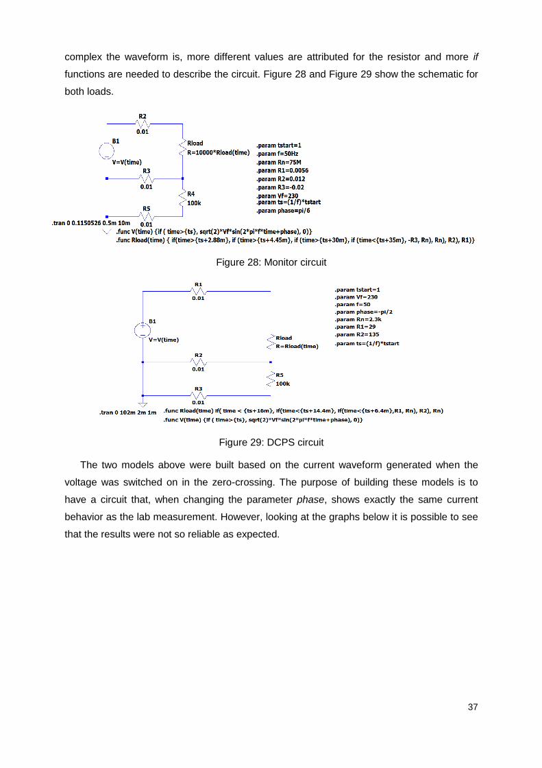
37
complex the waveform is, more different values are attributed for the resistor and more if
functions are needed to describe the circuit. Figure 28 and Figure 29 show the schematic for
both loads.
Figure 28: Monitor circuit
Figure 29: DCPS circuit
The two models above were built based on the current waveform generated when the
voltage was switched on in the zero-crossing. The purpose of building these models is to
have a circuit that, when changing the parameter phase, shows exactly the same current
behavior as the lab measurement. However, looking at the graphs below it is possible to see
that the results were not so reliable as expected.

38
Figure 30: Validation for the monitor at 0°
Figure 31: Validation for the monitor at 90°
For the phase 0°, it’s clear the similarity between the original (FlukeView) and the
computational model (LTspice) waveforms. When the source was switched on to 90°, the
similarity between the waveforms has suffered a considerable decrease. The peaks’
amplitude increases when the phase is set nearby 90° and the pulse width does not follow
the changes observed in the real load. As shown in Figure 31, the time duration of the peak
changes, but this is not followed by the model, whose pulse width is a constant independent
of the changes in phase.
The results for the DCPS are similar. For the zero-crossing they show a good similarity,
but for the 90° the similarity is even lower than for the monitor.

39
Figure 32: Validation for the DCPS at 0°
Figure 33: Validation for the DCPS at 90°
In the figure above, not only the pulse width changes, but the interval between the two
peaks changes with the changing in phase as well. It’s possible to see that the peaks are
much closer from each other in the 90° switch than in the 0° switch. In the simulation, the
distance between them keeps the same, which makes it much more different from the real
load behavior and increases the error between the two curves.
The error between the interpolated data and the FlukeView curve was calculated based
on the formula:
𝑒 =1
𝑛∑(𝑓𝑖 − 𝑙𝑡𝑖)2
𝑛
𝑖=0
where n is the number of samples, 𝑓𝑖 is the FlukeView value of sample i and 𝑙𝑡𝑖 is the
interpolated LTspice value of the same sample i. The error was calculated point by point and
plotted in a graph versus the time in order to have a better visualization of where the most
expressive errors are.

40
Figure 34: Error for the monitor in phase 0°.
Figure 35: Error for the monitor in phase 90°.
Analyzing the graphs, it’s noticeable that the higher errors occur on the peaks. This was
expected, since it’s difficult to simulate this variation of current exactly in the same way.
Furthermore, the order of magnitude of the error changes a lot from the 0° to the 90°. In the
first case, the higher error magnitude was around 0,02, whereas in the second case it was a
bit more than 0,25.
For the DCPS, the following results were obtained:

41
Figure 36: Error for the DCPS in phase 0°.
Figure 37: Error for the DCPS in phase 90°.
In this case, the DCPS LTspice model did not represent so faithfully the real load
behavior like the monitor did. Further improvements can be done in this model, in a way that
both the DCPS and the monitor have their models reliable even when there are changes in

42
the phase. A table with the errors for all the simulated loads can be found in the next chapter,
Results and Discussion.

43
5. RESULTS AND DISCUSSION
Considering all the graphs present in this report, two tables presenting the validation of
the models were created in order to quantify the average error associated to each load. For
loads of Type A to Type F, the error is presented on Table 1.
Table 1: Loads Error
TYPE LOAD NAME ERRO
R
A
DCPS VWCB receiver
modules
0.0090
57
2nd Optical DL DVI splitter 0.0157
94
Dual Link Splitter 0.0057
34
B
2nd DCPS VWCB receiver
modules
0.0046
46
3nd DCPS VWCB receiver
modules
0.0069
93
C
MCS Monitor 1.3163
03
CRCB Monitor 0.2165
05
D 16x16 DVI matrix switch 3.134
SIB 8.0266
85
E
Host PC 40.941
55
IP PC F 16.774
466
IP PC L 16.562
550

44
Flexvision Dell PC 0.0436
5
F
Tube Cooler F 30.667
845
Tube Cooler L 7.5102
07
Analyzing Table 1, it is remarkable that, in general, the created models have a high level
of similarity presenting an error smaller than 10. However, in loads from type E, except for
the Dell PC, the error is larger than the expected. Loads from this type are basically
composed by two peaks, one in the negative and one in the positive Y axis area. When these
curves are represented in LTspice, the peaks from the original and from the created load do
not match exactly because the LTspice curve tends to follow the voltage waveform. This is
something undesirable, because the shape of the inrush peak sometimes is really steep and
short, whereas in the simulation it’s only possible to have an inrush peak that looks like a
sine wave.
In the case of the Tube Cooler F, the high magnitude of the error can be explained based
on the fact that there is a shifting between the waveform provided by FlukeView and the one
provided by LTspice interpolation. Although there is a good matchup between the mentioned
waveforms when the graphs are visually analyzed, the magnitude of the average error is
surprisingly big. It might be that due to this shifting, the points analyzed for the interpolation
are not in the same time in FlukeView, causing also some shifting in the error plot.
Table 2 presents the average error of the monitor and the DCPS analyzed in the Lab. As
already mentioned, all the loads were created based on a zero phase switch-on. This way,
when the switch-on happens in a different phase, the model presented some unexpected
behavior and some differences when comparing to the original waveform. By analyzing this
table, it looks like when the phase is changed the results are reasonable, but looking at the
plots, the curves does not matchup so well. Surprisingly, in both models the error of some
non-zero phases is even smaller than in the zero phase. All these facts shows that the
method used for the error calculation might not be the most appropriate for this validation.
According to statistics definitions, the average error is one of many ways to quantify the
difference between values implied by an estimator and the true values of the quantity being
estimated. Unfortunately, the use of this method suppresses the most expressive errors,
giving some kind of wrong impression about the model behavior. [7]

45
Table 2– Monitor and DCPS Errors
ERROR
LOAD 𝟎° 𝟑𝟎° 𝟔𝟎° 𝟗𝟎° −𝟑𝟎° −𝟔𝟎° −𝟗𝟎°
Monitor 0.180778 0.001128 0.002449 1.087465 1.04612 0.003399 1.480049
DCPS 0.0037
75
1.519
495
0.015
159
0.017
271
0.00
799
0.028
657
0.022
769
Considering the analyses of both tables and of the all graphs present in this report, it can
be said that the models are a nice representation of the corresponding original one, offering
a quick and easy way of observing some complex kind of loads when the source is switched
on at zero phase and different phases. Although the results present in these tables are
reasonable, the error calculation method could be improved in the future in order to increase
the quality of the building models.

46
6. CONCLUSIONS
The aim of this assignment was the development of computational models capable of
offering reliable results in a short period of time and that provide the analysis of the inrush
behavior associated to loads that take part in a medical room. During the model creation`s
period, many ideas came up in order to generate the required current waveform in a circuit
composed only by resistors, capacitors and inductors. But also with the ideas, a lot of
troubles and difficulties emerged until the best model was chosen. In parallel with the load
model development, a magnetic simulation, also in LTspice, was created in order to analyze
how magnetic components behave under the core saturation.
After some non-efficient methods to obtain the required inrush behavior, it was decided to
describe a resistor using if functions in order to obtain the closest pulse width and current
peak amplitude to the original as possible. Since that, all the loads were divided in six
different types that present the same characteristics and could be defined using the same if
function structure, changing only values related to the time and amplitude parameters. By
using this method, the results obtained for the loads were, by looking, really satisfying, but it
became necessary to validate these models and see if the relation with the original
waveforms was as good as expected.
In order to validate all the results, it became necessary to interpolate the points that came
from LTspice with the aim of reaching the same sampling numbers and time step that comes
from FlukeView. Once interpolated, the average error between the waveforms could be
calculated.
Tables 1 and 2 present the error found for all the building loads. As already discussed, it
is remarkable that, in general, the created models have a high level of similarity, most of
them presenting an error smaller than 10. Though the tables present such good results,
some loads still need improvements and the error calculation method is still not the most
efficient, since the use of the average error method is not really expressive when an analysis
of the error in a determinate period of time is required.
In conclusion, considering all the results obtained, it can be said that the models created
in LTspice are a very good way to simulate and represent real life loads in a medical room. A
good recommendation to the next group that will take place in this project is to look for
different ways to calculate these errors, improving the loads that are not so accurate.
Moreover, further improvements have to be done in the magnetic components simulation, in
order to obtain a model that represents low-frequency hysteresis. And finally, it’s necessary

47
to make some changes in the computational model, making it compatible with the real load
behavior even when the user changes the switch-on phase.

48
APPENDIX A – LOAD MODELING
In order to visualize one of the most expressive behaviors of the load, the inrush current,
a few techniques to vary the impedance of the computational load model were applied. In the
beginning, a single load was designed using first a variable resistor. In this case, a resistor
was set to have its value increased during the same period of time. The initial value was set
and increased by a defined increment until it reaches a predetermined final value. The circuit
analyzed using this variable resistor is illustrated in Figure 38.
Figure 38: A single phase source with a variable resistor
The waveforms for voltage and current on the load are illustrated in Figure 39.
Figure 39: Output voltage and current on the resistor

49
The inrush current could not be visualized in this model, so it was necessary to choose
another way to represent the load. The second step taken was based on a varistor. A varistor
is an electronic component with a nonlinear current–voltage characteristic, similar to a diode.
This kind of component is often used to protect circuits against excessive transient voltages
by incorporating them into the circuit in such a way that, when triggered, it will shunt the
current created by the high voltage away from sensitive components. The schematic is
illustrated in Figure 40. [8]
Figure 40: A single phase source with a varistor
The voltage waveforms on the voltage source, on the varistor terminals and on the load,
as well as the current waveforms on the voltage source and the on the load are presented in
Figure 41.

50
Figure 41: Output voltage and current on the varistor
By analyzing the figure above, the inrush current still could not be observed, only a
decrease on the current amplitude when the varistor is triggered. After testing both
techniques mentioned, a resistor was described as a mathematical function that could clearly
describe the inrush current and the current damping during the time. This resistor model was
already presented in “Software Simulation” in the Load Model Building section.

51
APPENDIX B – LOAD TYPES
The complete description of the load types is shown below.
Type A
Figure 42: 1st DCPS VWCB receiver modules (B-Cabinet)
Figure 43: 2nd Optical DL DVI splitter (B-Cabinet)
Figure 44: Dual Link splitter (B-Cabinet)

52
Type B
Figure 45: 2nd DCPS VWCB receiver modules (B-Cabinet)
Figure 46: 3rd DCPS VWCB receiver modules (B-Cabinet)
Type C
Figure 47: 2nd MCS monitors (WME 1.8) (M-Cabinet)

53
Figure 48: CRCB continuous (M-Cabinet)
Figure 49: CRCB switched (M-cabinet)
Type D
Figure 50: 16x16 DVI matrix switch (B-cabinet)
54
Figure 51: SIB (M-cabinet)
Type E
Figure 52: Host PC (M-Cabinet)
Figure 53: IP PC F (M-Cabinet)

55
Figure 54: IP PC L (M-Cabinet)
Figure 55: Flexvision Dell PC (B-cabinet)

56
Type F
Figure 56: Tube Cooler F (M-Cabinet)
Figure 57: Tube Cooler L (M-Cabinet)

57
APPENDIX C – COMPUTATIONAL MODEL
The graphs below are composed by four waveforms: the data import from the scopemeter
(FlukeView), the data import from the model created in LTspice, the interpolation of LTspice
data and the error between the FlukeView curve and the interpolated curve.
In all of the graphs present in this appendix, the X axis represents the time
in seconds, the primary Y axis (on the left) represents the amplitude in Amperes, while the
secondary Y axis (on the right) represents the amplitude of the error.
Type A
Figure 58: 1st DCPS VWCB receiver modules
Figure 59: 2nd Optical DL DVI splitter

58
Figure 60: Dual Link Splitter
Type B
Figure 61: 2nd DCPS VWCB receiver modules.
Figure 62: 3nd DCPS VWCB receiver modules

59
In loads of Type A and B, a capacitor was included in series with the resistor. This was
necessary because without an active component, the resulting current of a pure resistive
load has the shape of a sine wave, whereas the real inrush behavior presents a shorter and
steeper pulse width. Therefore, in all of the DCPS loads, capacitors of 600µF and 300µF
were added to the circuit and also in the 2nd Optical Dual DVI Splitter (a capacitor of 7mF)
and in the Dual Link Splitter (200µF).
Type C
Figure 63: MCS Monitor
Figure 64: CRCB Monitor

60
Type D
Figure 65: 16x16 DVI matrix switch
Figure 66: SIB
Type E
Figure 67: Host PC

61
Figure 68: IP PC F
Figure 69: IP PC L
Figure 70: Flexvision Dell PC
In the schematics that represents the IP PC F and the IP PC L, one capacitor of 200𝑚𝐹
was included in parallel with the resistor. This way, the peak in the positive area of the graph
could be thinner, fitting in a better way the original waveform.

62
Type F
Figure 71: Tube Cooler F
Figure 72: Tube Cooler L
In the Figures 71 and 72 above, the interpolation process did not cause many distortions
in the waveform. This way, most of the curves before and after the interpolation are overlaid.
Furthermore, the error curves are smaller because the current waveforms were prioritized.

63
APPENDIX D – LAB MEASUREMENTS
The complete waveforms obtained in the Lab, for the monitor and for DC Power Supply
(DCPS), are present below. In the figures, the red curve is the input voltage and the blue
curve is the current in the load.
Figure 73: Monitor (power switched in phase 𝟎°)
Figure 74: Monitor (power switched in phase 𝟑𝟎°)
Figure 75: Monitor (power switched in phase 𝟔𝟎°)

64
Figure 76: Monitor (power switched in phase 𝟗𝟎°)
Figure 77: Power Supply (power switched in phase 𝟎°)
Figure 78: Power Supply (power switched in phase 𝟑𝟎°)

65
Figure 79: Power Supply (power switched in phase 𝟔𝟎°)
Figure 80: Power Supply (power switched in phase 𝟗𝟎°)
To guarantee that the inrush behavior was the same for the correspondent negative
phase, extra measurements including the phases −30°, −60° and −90° were done. The
correspondent waveforms are present from Figure 81 to Figure 86.
Figure 81: Monitor (power switched in phase −𝟑𝟎°)

66
Figure 82: Monitor (power switched in phase −𝟔𝟎°)
Figure 83: Monitor (power switched in phase −𝟗𝟎°)
Figure 84: Power Supply (power switched in phase −𝟑𝟎°)

67
Figure 85: Power Supply (power switched in phase −𝟔𝟎°)
Figure 86: Power Supply (power switched in phase −𝟗𝟎°)
The graphs comparing the current waveforms from the models that have been created in
LTspice and the ones measured in the Lab, when the source is switched-on on 0°, 30°, 60°,
90°,−30°, −60°, −90° are present below.
Figure 87: Monitor Phase 𝟎°

68
Figure 88: Monitor Phase 𝟑𝟎°
Figure 89: Monitor Phase 𝟔𝟎°
Figure 90: Monitor Phase 𝟗𝟎°

69
Figure 91: Monitor Phase −𝟑𝟎°
Figure 92: Monitor Phase −𝟔𝟎°
Figure 93: Monitor Phase −𝟗𝟎°

70
Figure 94: DCPS Phase 𝟎°
Figure 95: DCPS Phase 𝟑𝟎°
Figure 96: DCPS Phase 𝟔𝟎°

71
Figure 97: DCPS Phase 𝟗𝟎°
Figure 98: DCPS Phase −𝟑𝟎°
Figure 99: DCPS Phase −𝟔𝟎°
72
Figure 100: DCPS Phase −𝟗𝟎°

73
REFERENCES
[1] http://www.healthcare.philips.com
[2] Chen, C. and Wu, Q. 2012. Power Distribution System (PDS) Source and Load
Modelling. Philips Healthcare, Best.
[3] Liu, Y. 2011. Power Distribution System (PDS). Philips Healthcare, Best.
[4] http://www.energynetworks.org/info/faqs/electricity-distribution-map.html
[5] Boeh-Ocansey,E. and Anizoba, J. 2012. Load Modeling and Behavioral Analysis:
Verification and Testing of Power Distribution Unit.
[6] Sandler, S. Spice Modeling of Magnetic Components. October 7, 2005.
[7]http://www.math-
interactive.com/products/calgraph/help/fit_curve_to_data/root_mean_squared_error.htm
[8] http://www.princeton.edu/~achaney/tmve/wiki100k/docs/Varistor.html