power factor correction – why and how? drivers for power factor correction what is power factor...
TRANSCRIPT

Renesas Electronics America Inc.© 2012 Renesas Electronics America Inc. All rights reserved.
Power Factor Correction –Why and How?
© 2012 Renesas Electronics America Inc. All rights reserved.2
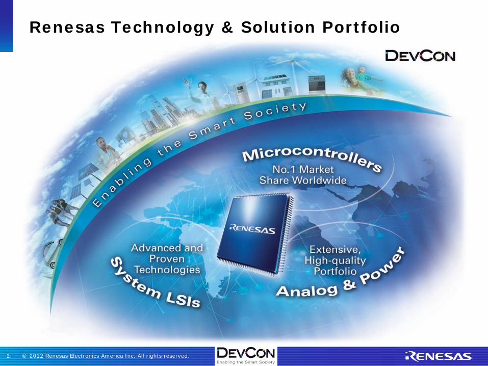
Renesas Technology & Solution Portfolio

© 2012 Renesas Electronics America Inc. All rights reserved.3
Microcontroller and Microprocessor Line-up
Wide Format LCDs Industrial & Automotive, 130nm 350µA/MHz, 1µA standby
44 DMIPS, True Low Power
Embedded Security, ASSP
165 DMIPS, FPU, DSC
1200 DMIPS, Performance1200 DMIPS, Superscalar
500 DMIPS, Low Power
165 DMIPS, FPU, DSC
25 DMIPS, Low Power
10 DMIPS, Capacitive Touch
Industrial & Automotive, 150nm 190µA/MHz, 0.3µA standby
Industrial, 90nm 242µA/MHz, 0.2µA standby
Automotive & Industrial, 90nm 600µA/MHz, 1.5µA standby
Automotive & Industrial, 65nm 600µA/MHz, 1.5µA standby Automotive, 40nm
500µA/MHz, 35µA deep standby
Industrial, 40nm 242µA/MHz, 0.2µA standby
Industrial, 90nm 1mA/MHz, 100µA standby
Industrial & Automotive, 130nm 144µA/MHz, 0.2µA standby
2010 2013
32
-bit
8/16
-bit
© 2012 Renesas Electronics America Inc. All rights reserved.4
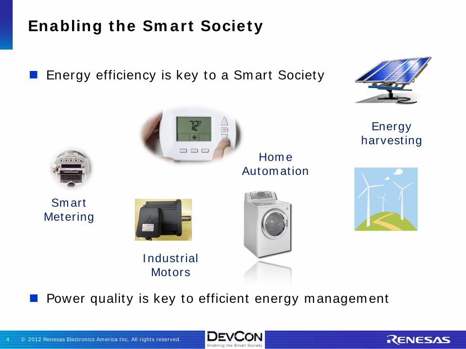
Enabling the Smart Society
IndustrialMotors
Smart Metering
Energy harvesting
Home Automation
Energy efficiency is key to a Smart Society
Power quality is key to efficient energy management

© 2012 Renesas Electronics America Inc. All rights reserved.5
Agenda Market drivers for Power Factor Correction
What is Power Factor and why do we need to correct it?
Definition of Power Factor (PF)
What causes PF degradation
Impacts of bad PF on power distribution and billings
How do we correct bad Power Factor?
Basic PFC topologies
Renesas PFC Solutions
Analog and Digital Solutions
Implementation with Renesas MCU and Analog & Power devices
Summary

© 2012 Renesas Electronics America Inc. All rights reserved.6
PFC Market Drivers
© 2012 Renesas Electronics America Inc. All rights reserved.7
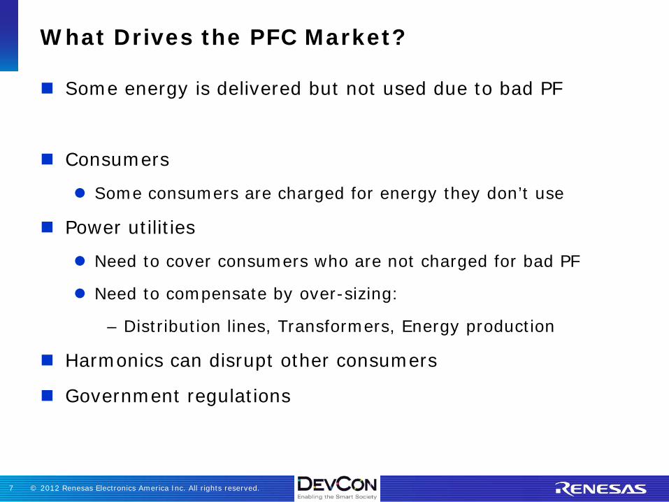
What Drives the PFC Market?
Some energy is delivered but not used due to bad PF
Consumers
Some consumers are charged for energy they don’t use
Power utilities
Need to cover consumers who are not charged for bad PF
Need to compensate by over-sizing:
– Distribution lines, Transformers, Energy production
Harmonics can disrupt other consumers
Government regulations

© 2012 Renesas Electronics America Inc. All rights reserved.8
Real Power: P = 400 W (Watts)
Apparent Power: S = 120V x 5.1A = 612 VA (Volt Ampere)
Power Factor:
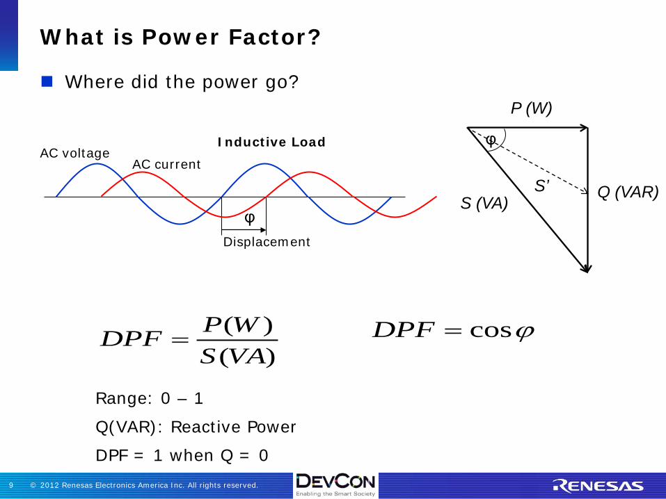
What is Power Factor?
~AA AP
AC Motor
WattmeterAmmeter
120V 60Hz
)()(
VASWPPF =
5.1 A 400W
PF = 400/612 = 0.653
© 2012 Renesas Electronics America Inc. All rights reserved.9
What is Power Factor?
Where did the power go?
AC currentAC voltage
φDisplacement
)()(
VASWPDPF = ϕcos=DPF
Range: 0 – 1
Q(VAR): Reactive Power
DPF = 1 when Q = 0
P (W)
Q (VAR)S (VA)
φ
S’
Inductive Load
© 2012 Renesas Electronics America Inc. All rights reserved.10
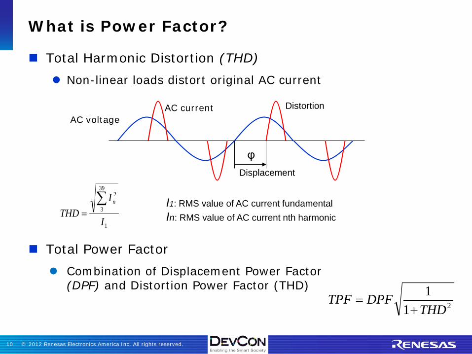
What is Power Factor?
Total Harmonic Distortion (THD) Non-linear loads distort original AC current
Total Power Factor Combination of Displacement Power Factor
(DPF) and Distortion Power Factor (THD)
AC currentAC voltage
φDisplacement
Distortion
1
39
3
2
I
ITHD
n∑=
I1: RMS value of AC current fundamentalIn: RMS value of AC current nth harmonic
211
THDDPFTPF
+=

© 2012 Renesas Electronics America Inc. All rights reserved.11
What causes PF degradation?
Inductive loads store reactive power and cause current lag
Non-linear loads with switching elements distort the original AC current and introduce harmonics
Total Power Factor
Bad PF:
1<TPF
211
THDDPFTPF
+=

© 2012 Renesas Electronics America Inc. All rights reserved.12
Question 1
What causes PF degradation?
A. Resistive loads
B. Inductive loads
C. Capacitive loads
D. Non-linear loads
E. B, C, D
F. None of the above
© 2012 Renesas Electronics America Inc. All rights reserved.13
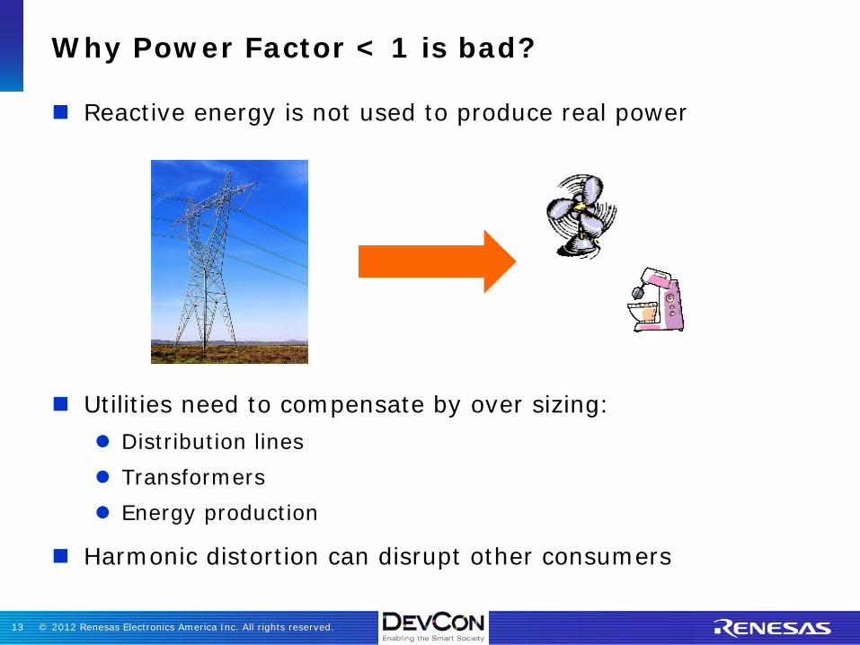
Why Power Factor < 1 is bad?
Reactive energy is not used to produce real power
Utilities need to compensate by over sizing: Distribution lines Transformers Energy production
Harmonic distortion can disrupt other consumers

© 2012 Renesas Electronics America Inc. All rights reserved.14
Power Factor Correction
© 2012 Renesas Electronics America Inc. All rights reserved.15
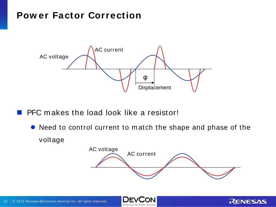
Power Factor Correction
PFC makes the load look like a resistor!
Need to control current to match the shape and phase of the
voltage
AC currentAC voltage
φDisplacement
AC currentAC voltage
© 2012 Renesas Electronics America Inc. All rights reserved.16
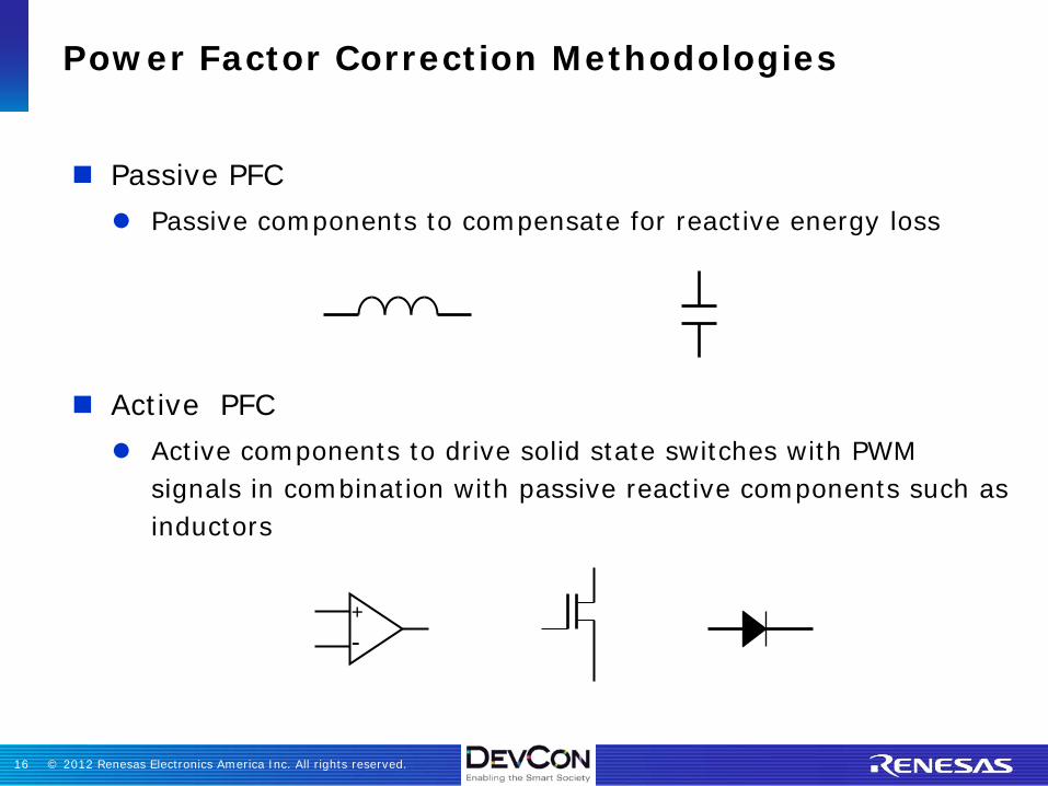
Power Factor Correction Methodologies
Passive PFC Passive components to compensate for reactive energy loss
Active PFC Active components to drive solid state switches with PWM
signals in combination with passive reactive components such as inductors
+-

© 2012 Renesas Electronics America Inc. All rights reserved.17
Passive PFC
Control harmonic current using filter
Expensive large high-current inductor
No automatic adjustment for wider AC input power
DC output varies with AC input voltage
Passive Power Factor Correction

© 2012 Renesas Electronics America Inc. All rights reserved.18
Active PFC Input current is controlled to follow the shape and phase of
input AC voltage
Transistor Q is switched ON/OFF at a PWM rate
Most common configuration – Boost converter
Efficiency is affected by Q switching losses and diode recovery
Active Power Factor Correction
Q
© 2012 Renesas Electronics America Inc. All rights reserved.19
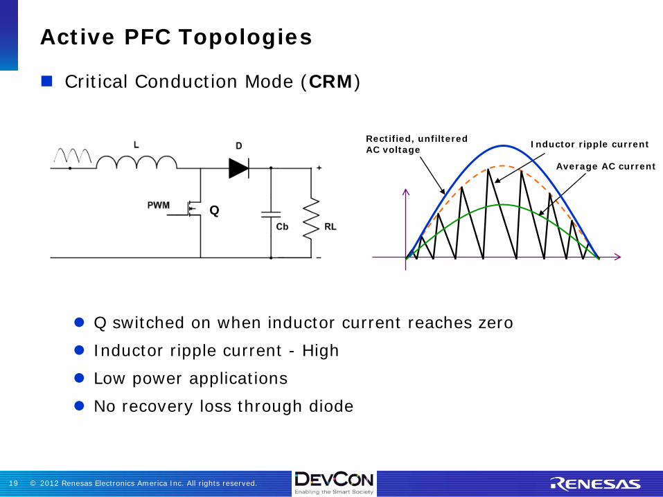
Active PFC Topologies
Critical Conduction Mode (CRM)
Q switched on when inductor current reaches zero Inductor ripple current - High Low power applications No recovery loss through diode
Q
Rectified, unfilteredAC voltage
Average AC current
Inductor ripple current

© 2012 Renesas Electronics America Inc. All rights reserved.20
Active PFC Topologies
Continuous Conduction Mode (CCM)
Q switched on before the inductor current reaches zero Inductor ripple current – Low High power applications Recovery loss through the diode
Rectified, unfilteredAC voltage
Average AC current
Inductor ripple current
Q
© 2012 Renesas Electronics America Inc. All rights reserved.21
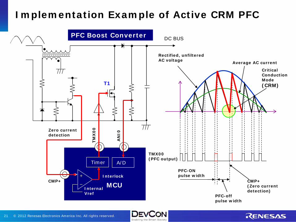
Implementation Example of Active CRM PFC
CMP+ (Zero current detection)
TMX00 (PFC output)
PFC-ON pulse width
Rectified, unfilteredAC voltage
PFC-off pulse width
Average AC current
CMP+
TMX
00
AN
I0
Interlock
Zero current detection
Internal Vref
T1
DC BUS
Critical Conduction Mode(CRM)
PFC Boost Converter
MCU
Timer A/D

© 2012 Renesas Electronics America Inc. All rights reserved.22
Two channel interleaved
Single channel
Active PFC Topologies
D1
Q1~120V
AC
C PFC Cb
L1
D1
Q1~120V
AC
C PFC Cb
L1
D2
L2
Q2
Reduced current ripple
Q1
IL1
Q1
IL1
Q2
IL2
IL1+IL2

© 2012 Renesas Electronics America Inc. All rights reserved.23
Effect of High-frequency Switching
Harmonics and inductor current ripple can disrupt other consumers Regulation standards apply – IEC61000-2-2
Higher ripple current will require better filters with multiple stages
Q
~120VAC
L
L
C C

© 2012 Renesas Electronics America Inc. All rights reserved.24
Advantages of Interleaving
Reduced current ripple Size and number of input filters can be reduced
Size of inductors, capacitor, switching devices can be reduced
Overall efficiency is increased
© 2012 Renesas Electronics America Inc. All rights reserved.25
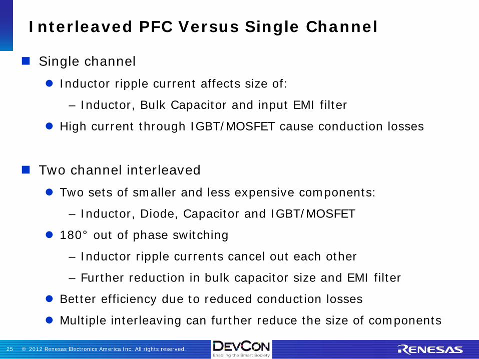
Interleaved PFC Versus Single Channel
Single channel Inductor ripple current affects size of:
– Inductor, Bulk Capacitor and input EMI filter
High current through IGBT/MOSFET cause conduction losses
Two channel interleaved Two sets of smaller and less expensive components:
– Inductor, Diode, Capacitor and IGBT/MOSFET
180° out of phase switching
– Inductor ripple currents cancel out each other
– Further reduction in bulk capacitor size and EMI filter
Better efficiency due to reduced conduction losses
Multiple interleaving can further reduce the size of components

© 2012 Renesas Electronics America Inc. All rights reserved.26
Interleaved PFC versus Single Channel
Item Single Channel 2-Ch InterleavedRipple current Large SmallInductor 1 large 2 small (less $)Transistor 1 large 2 small (less $)Diode 1 large (SiC?) 2 small (less $)Bulk capacitor Large SmallEMI filter Large SmallEfficiency Good Better
CCM topology for large power application (>300W)
© 2012 Renesas Electronics America Inc. All rights reserved.27
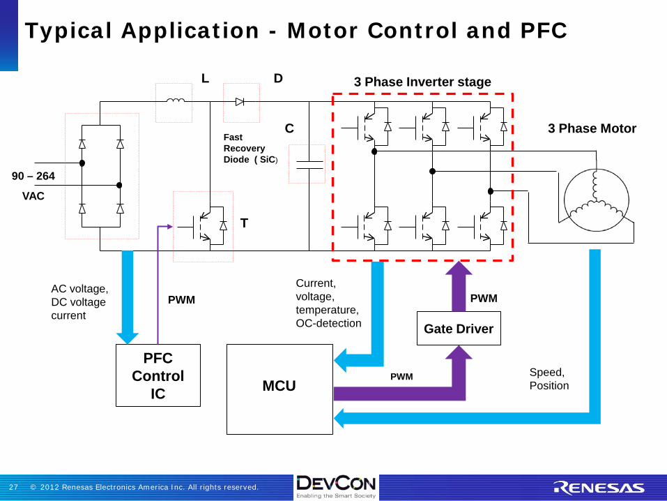
Typical Application - Motor Control and PFC
MCU
90 – 264
VAC
Gate Driver
PWM
PWMCurrent, voltage, temperature,OC-detection
PWM
Fast Recovery Diode ( SiC)
L
C
PFC Control
IC
AC voltage,DC voltagecurrent
3 Phase Inverter stageD
T
3 Phase Motor
Speed,Position

© 2012 Renesas Electronics America Inc. All rights reserved.28
Digital PFC for Motor Control Inverter
MCU
90 – 264
VAC
Gate Driver
PWM
PWMCurrent, voltage, temperature,OC-detection
PWM
Fast Recovery Diode ( SiC)
L
C
AC voltage,DC voltagecurrent
3 Phase Inverter stageD
T
3 Phase Motor
Speed,Position

© 2012 Renesas Electronics America Inc. All rights reserved.29
Renesas PFC Solutions
Renesas offers a variety of analog and digital devices to support PFC
Analog: PFC Controller ICs Single channel and interleaved
CCM and CRM topologies
Internal MOSFET/IGBT driver
Digital: MCUs with integrated peripherals High performance CPU with FPU and 10ns flash access
Internal PGAs and Comparators
High-speed ADC with multiple S&H
Fast over-current protection by hardware
Fast interrupt response

© 2012 Renesas Electronics America Inc. All rights reserved.30
Analog PFC Solutions

© 2012 Renesas Electronics America Inc. All rights reserved.31
PFC Controllers– CCM (Continuous Conduction Mode)– CRM (Critical Conduction Mode)
PFC Boost Switch– Super Junction MOSFETs for high frequency (> 50 kHz), up to
2.5 kW– High Speed, Low Vceon, IGBTs for lower frequency (< 40 kHz)
and above 2.5 kW
PFC Boost Diode (SiC)
Support and Collateral Datasheet Evaluation Boards Technical Support
Renesas Offers Complete Analog PFC Solutions

© 2012 Renesas Electronics America Inc. All rights reserved.32
Mode Part # Features Applications
CCM
Interleaved R2A20114R2A20104
Small current rippleAverage SW noiseMore complex circuit
ServerAir conditionerInduction heating
Single R2A20115 Large current rippleLarge SW noiseSimple circuit
Plasma TVPCOffice automation
CRM
Interleaved R2A20132R2A20118AR2A20117R2A20112
Small current rippleAverage SW noiseMore complex circuit
Air conditionerPlasma TVPCOffice automation
Single R2A20113 Large current rippleLarge SW noiseSimple circuit
LCD monitorAC adaptorLCD projector
Renesas Analog PFC Controller Solutions

© 2012 Renesas Electronics America Inc. All rights reserved.33
Current transformers
CCM Interleaved PFC Controllers 2A20114/20104
Phase drop control input Internal / external clock can be used 20104 can use current transformer
© 2012 Renesas Electronics America Inc. All rights reserved.34
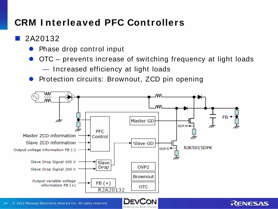
CRM Interleaved PFC Controllers 2A20132
Phase drop control input OTC – prevents increase of switching frequency at light loads
— Increased efficiency at light loads Protection circuits: Brownout, ZCD pin opening
© 2012 Renesas Electronics America Inc. All rights reserved.35
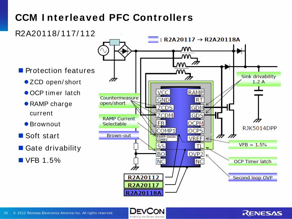
CCM Interleaved PFC Controllers
Protection featuresZCD open/shortOCP timer latchRAMP charge
currentBrownout
Soft start Gate drivability VFB 1.5%
R2A20118/117/112

© 2012 Renesas Electronics America Inc. All rights reserved.36
Digital PFC Solutions
© 2012 Renesas Electronics America Inc. All rights reserved.37
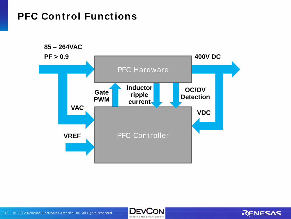
PFC Control Functions
PFC Controller
85 – 264VAC400V DC
Inductor ripple
currentGate PWM
OC/OV Detection
VREF
PFC Hardware
VACVDC
PF > 0.9

© 2012 Renesas Electronics America Inc. All rights reserved.38
PFC Control Functions – Input/Output
Control function Input Output
Output voltage Feedback voltage Constant DC bus voltage
AC voltage range AC voltage Adjust to 85-264VAC
Inductor currentIGBT current
AC voltage
Inductor current amplitudeSynchronize with AC voltage phase
Hardware protectionOver-currentOver-voltage
Under-voltage
Disable IGBT gate signals

© 2012 Renesas Electronics America Inc. All rights reserved.39
Digital PFC for Motor Control Inverter
Rx62T MCU
90 – 264
VAC
Gate Driver
PWM
PWMCurrent, voltage, temperature,OC-detection
PWM
Fast Recovery Diode ( SiC)
L
C
AC voltage,DC voltagecurrent
3 Phase Inverter stageD
T
3 Phase Motor
Speed,Position

© 2012 Renesas Electronics America Inc. All rights reserved.40
Interleaved PFC Reference Design
PFCCH1
Rx62T MCU board
PFCCH2
Auxiliary power
DC/DC converter
SICDiodes
395V3.8Aoutput
85-264 VAC input

© 2012 Renesas Electronics America Inc. All rights reserved.41
Complete PFC Solution from Renesas
RX62T/100pinR5F562TAADFP
IGBT:RJH60F4DPK
Diode:RJS6005TDPP-EJ(target)
IGBT:RJH60F4DPK
© 2012 Renesas Electronics America Inc. All rights reserved.42
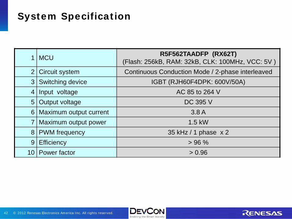
System Specification
1 MCU R5F562TAADFP (RX62T)(Flash: 256kB, RAM: 32kB, CLK: 100MHz, VCC: 5V )
2 Circuit system Continuous Conduction Mode / 2-phase interleaved3 Switching device IGBT (RJH60F4DPK: 600V/50A)4 Input voltage AC 85 to 264 V5 Output voltage DC 395 V6 Maximum output current 3.8 A7 Maximum output power 1.5 kW8 PWM frequency 35 kHz / 1 phase x 29 Efficiency > 96 %
10 Power factor > 0.96
© 2012 Renesas Electronics America Inc. All rights reserved.43
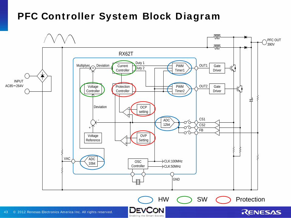
PFC OUT390V
GateDriver
VAC
VoltageReference
INPUTAC85~264V
FB
GND
OUT1
+
×
-
CurrentController
VoltageController
PWMTimer1
OUT2 GateDriver
ADC12bit
OCPsetting
OVPSetting
ProtectionController
Multiplyer
CS1CS2
OSCController
CLK:100MHzCLK:50MHz
PWMTimer2
RX62T
ADC10bit
Deviation
DeviationDuty 1Duty 2
PFC Controller System Block Diagram
ProtectionSWHW

© 2012 Renesas Electronics America Inc. All rights reserved.44
CS1 GD1
GD2
Controller Implementation
Control loops:Two-stage IIR filter
CC1
CC2
VC
CS2
VAC
VFB
CS1,2 - Current sensing Ch1,2VAC - AC Input voltageVFB - DC Output voltageCC1,2 - Current controller 1,2VC - Voltage controller

© 2012 Renesas Electronics America Inc. All rights reserved.45
Program Flow
Conversion start by GPT
Conversion complete interrupt
Voltage reference calculation
Voltage IIR filter controller
Current IIR filter controller
GPT PWM duty update
ADC conversion interrupt
12-Bit ADC
ADC to voltage calculation
Voltage controller
Current controller
PWM update
Main
Main
Interrupt
10-Bit ADC
VAC CS FB

© 2012 Renesas Electronics America Inc. All rights reserved.46
Signal name MCU Peripheral Pin Name I/O Resolution Functions
GD1 GPT0 GTIOC0A-A OUT 20ns PWM for IGBT1 gate
GD2 GPT1 GTIOC1A-A OUT 20ns PWM for IGBT1 gate
VFB 12-Bit ADC0 AN000 IN 12bit Output DC voltage sensing
CS2 12-Bit ADC0 AN001 IN 12bit IGBT1 current sensing
CS2 12-Bit ADC0 AN002 IN 12bit IGBT2 current sensing
VAC 10-Bit ADC AN2 IN 10bit Input AC voltage sensing
RX62T MCU Resources Used

© 2012 Renesas Electronics America Inc. All rights reserved.47
CS1
CS2
IL1
GD2
FB
IL2
0.02Ω
0.02Ω
uPC844G2
uPC844G2
uPC844G2
RX62T Peripherals used for PFC
16-Bit CMT 4 channel
Multi purpose timer
Flash up to 256KB
Data Flash 8KB(30k times E/W)
RAM 16KB
RX CPU(100 MHz)
FPUMultiplier, Divider,
Multiply, Accumulate
Ch 3&43-ph PWM
Ch 1&22 Encoder Inputs
Ch 0Hall / BEMF Input
Ch 5Dead-time compensation
Ch 6&73-ph PWM
16-Bit MTU3
12bit ADC 4-ch
x 2
3 PGA3 Comp
x 2
10bit ADC 12-ch
16-bit PWM Timer GPT0
16-bit PWM Timer GPT1
16-bit PWM Timer GPT2
16-bit PWM Timer GPT3
390VDC
~
CS1CS2
VFB
VAC
GPT
RX 62T
GD1
GD2
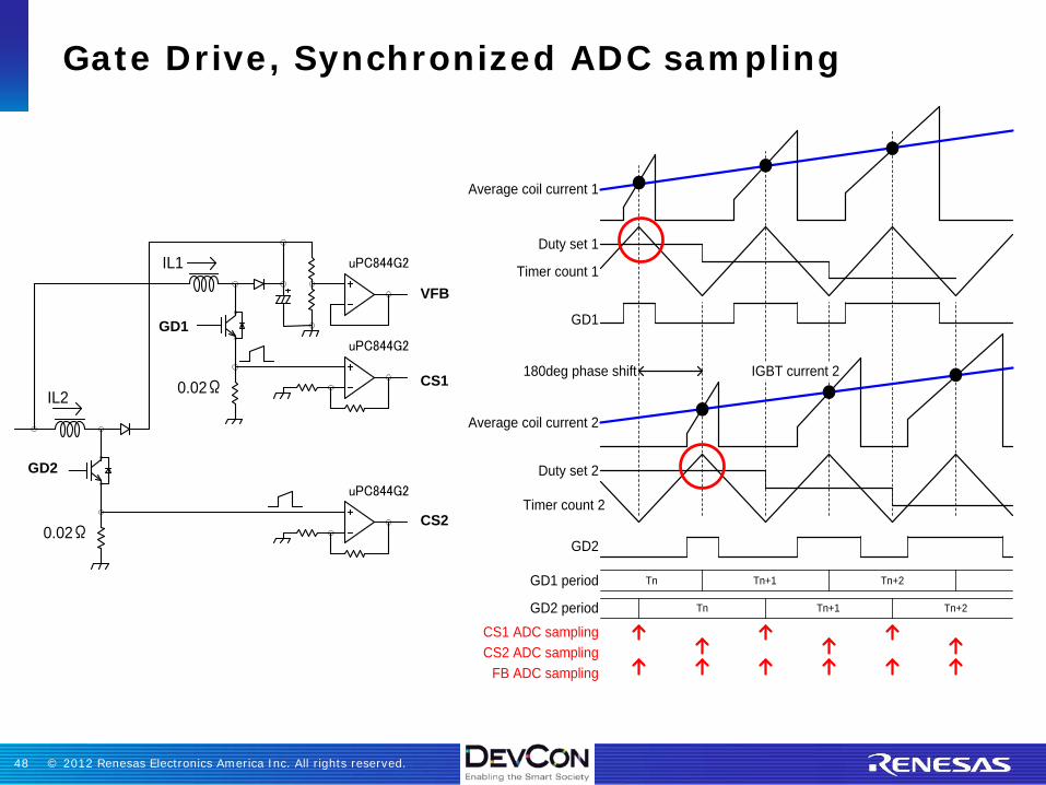
© 2012 Renesas Electronics America Inc. All rights reserved.48
CS1
CS2
IL1
GD2
FB
IL2
0.02Ω
0.02Ω
uPC844G2
uPC844G2
uPC844G2
GD1
Timer count 1
Duty set 1
Average coil current 1
GD2
Timer count 2
Duty set 2
Average coil current 2
GD1 period
CS1 ADC sampling
Tn Tn+1 Tn+2
GD2 period
FB ADC sampling
Tn Tn+1 Tn+2
180deg phase shift
CS2 ADC sampling
IGBT current 2
Gate Drive, Synchronized ADC sampling
GD1
GD2
VFB
CS1
CS2

© 2012 Renesas Electronics America Inc. All rights reserved.49
RX62T
POE0#
PWM-FB
MTIOC3BPFC-GD1
PFC-GD2
PWM-GD
MTIOC4A
MTIOC4B
3.33V
+5VPFC-OUT
2MΩ
18.56kΩ
5.1kΩ2kΩ
3.33V
PWM-OUT
20kΩ
PFC-FB
PWM-OUT
PFC-OUT
R5F562TAADFP
10k
OVP_PWM
OVP_PFC
* 1. Protection by external hardware* 2. Protection by internal hardware by POE function
* 1* 2
Overvoltage Protection by Hardware
- Example of PFC and DC/DC converter

© 2012 Renesas Electronics America Inc. All rights reserved.50
AN000/AN101
AN001/AN101
AN002/AN102
ADC unit 0
Data Register 0
Data Register 1
Data Register 2
Data Register 3
S/H
Three S&H for sensing currents and voltage for interleaved PFC.
PGA (Programmable Gain Amp) with selectable gain
1 usec conversion time per channel at AVCC0=AVCC=4.0 to 5.5V.
AN003/AN103
Feedback Signal Measurement by 12-Bit ADC
PGA
PGA
PGA
S/H
S/H
Mul
tiple
xer
ADC
VFBPF_IN
VCSPF1_IN
VCSPF2_IN
VAC_IN

© 2012 Renesas Electronics America Inc. All rights reserved.51
Implementation with General Purpose Timers
4-Channels, 16-Bit counters, 100 MHz count clock
Phase shifted operation – 180° for interleaved PFC
Triangular wave with center aligned PWM
ADC conversion start trigger by timer
GTIOC0A-A/B
POE3
CPU interrupt for POE
AD trigger
CPU InterruptGTCCRA0
GPT0.GTCNT
ONGTIOC0A-A ONOFFOFF
ON OFF ONONOFF
OFF
GPT1.GTCNT
1. GTPR0,1: PWM frequency(35kHz)2. GTCCRA0,1: PWM duty
GTIOC1A-A
GTCCRA1
GPT0GTIOC0B-A/B
GTIOC1A-A/BAD trigger
CPU InterruptGPT1
GTIOC1B-A/B
GTIOC2A-A/BAD trigger
CPU InterruptGPT2
GTIOC2B-A/B
GTIOC3AAD trigger
CPU InterruptGPT3
GTIOC3B
Out
put p
rote
ct

© 2012 Renesas Electronics America Inc. All rights reserved.52
Example of PFC Control Trigger by GPT0
GTIOC0A output PFC gate drive
GTADTRAADC Trigger
ADC conversion start
ADC conversion end
PFC control start PFC control end
ADC conversion end interrupt
∆t
Register write Register write Register write Register write
aaaabbbbccccddddeeee
ffff
GPT0.GTCNTCounter value
bbbb ffff dddd
hhhhGTP0.GTPRPFC Cycle
hhhh
hhhhddddffffBuffer transfer at crest Buffer transfer at through Buffer transfer at crest
Time
GTP0.GTCCRCPFC Duty Cycle

© 2012 Renesas Electronics America Inc. All rights reserved.53
CPU BW for Interleaved PFC: 32% @35KHz
GD1
PFC control timing 28us
9us (32%)Control loop processing:
4.5us 4.5us

© 2012 Renesas Electronics America Inc. All rights reserved.54
Input AC voltage
Input AC current
Inductor current
Output voltage ripple
AC Current Waveforms @1.5KW – 100V AC input
1.5KW @ 100V AC Input

© 2012 Renesas Electronics America Inc. All rights reserved.55
Each GPT channel can generate HR-PWM for two outputs independently Minimum resolution is 1/32 of normal resolution: 312.5psec @100MHz 390.0psec @80MHz
GTCNT
Comparator
GTCCRF
GTCCRB GTCCRA
Controller
GTDVU GTPR
GTCCRD
GTCCRE GTCCRC
GTPBR
Out
put
cont
rol
GTADTRAGTADTBRA
GTADTRB
Out
put p
rote
ct
ExternalTrigger.
PWM1
PWM2
POEx
AD trigger
CPU interrupts
CPU Interrupt
GTADTBRB
GTADTDBRA GTADTDBRB
GTPDBR
Inpu
t co
ntro
l
GTDBUGTDVDGTDBD
Com
para
tor
inpu
t
Hig
h re
solu
tion
rising falling
GTTCRA GTTCRA
GTDLYRA GTDLYFA
GTIOCA
GTTCRA
15 0Upper 16bit Lower 5bit
+GTDLYRA
+GTDLYFA
04
GTDLYFAGTDLYRA
Rx62G High Resolution PWM Timer

© 2012 Renesas Electronics America Inc. All rights reserved.56
Question 2
What PFC method is used in the Renesas digital reference design?
A. Single-channel PFC in Critical Conduction Mode (CRM)
B. Single-channel PFC in Continuous Conduction Mode (CCM)
C. Dual-channel interleaved in Continuous Conduction Mode (CCM)
D. None of the above

© 2012 Renesas Electronics America Inc. All rights reserved.57
Summary Market drivers for Power Factor Correction
What is Power Factor and why do we need to correct it?
Definition of Power Factor (PF)
What causes PF degradation
Impacts of bad PF on power distribution and billings
How do we correct bad Power Factor?
Basic PFC topologies
Renesas PFC Solutions
Analog and Digital Solutions
Implementation with Renesas MCU and Analog & Power devices

© 2012 Renesas Electronics America Inc. All rights reserved.58
Questions?

© 2012 Renesas Electronics America Inc. All rights reserved.59
Enabling the Smart Society
IndustrialMotors
Smart Metering
Energy harvesting
Home Automation
Energy efficiency is key to a Smart Society
Power quality is key to efficient energy management

Renesas Electronics America Inc.© 2012 Renesas Electronics America Inc. All rights reserved.