power5 ewen cheslack-postava case taintor jake mcpadden
TRANSCRIPT

POWER5
Ewen Cheslack-Postava
Case Taintor
Jake McPadden
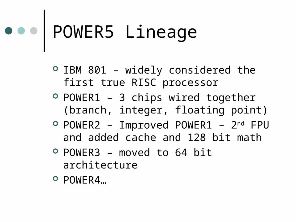
POWER5 Lineage
IBM 801 – widely considered the first true RISC processor
POWER1 – 3 chips wired together (branch, integer, floating point)
POWER2 – Improved POWER1 – 2nd FPU and added cache and 128 bit math
POWER3 – moved to 64 bit architecture POWER4…
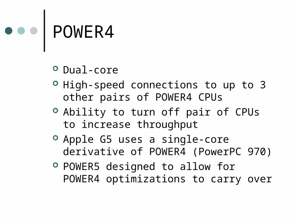
POWER4
Dual-core High-speed connections to up to 3 other
pairs of POWER4 CPUs Ability to turn off pair of CPUs to increase
throughput Apple G5 uses a single-core derivative of
POWER4 (PowerPC 970) POWER5 designed to allow for POWER4
optimizations to carry over

Pipeline Requirements
Maintain binary compatibility Maintain structural compatibility
Optimizations for POWER4 carry forward Improved performance Enhancements for server virtualization Improved reliability, availability, and
serviceability at chip and system levels

Pipeline Improvements
Enhanced thread level parallelism Two threads per processor core a.k.a Simultaneous Multithreading (SMT) 2 threads/core * 2 cores/chip = 4
threads/chip Each thread has independent access to L2
cache Dynamic Power Management Reliability, Availability, and Serviceability


POWER5 Chip Stats
Copper interconnectsDecrease wire resistance and reduce
delays in wire dominated chip timing paths
8 levels of metal 389 mm2

POWER5 Chip Stats
Silicon on Insulator devices (SOI) Thin layer of silicon (50nm to 100 µm) on insulating
substrate, usually sapphire or silicon dioxide (80nm) Reduces electrical charge transistor has to move
during switching operation (compared to CMOS)• Increased speed (up to 15%)• Reduced switching energy (up to 20%)• Allows for higher clock frequencies (> 5GHz)
SOI chips cost more to produce and are therefore used for high-end applications
Reduces soft errors


Pipeline
Pipeline identical to POWER4 All latencies including branch
misprediction penalty and load-to-use latency with L1 data cache hit same as POWER4
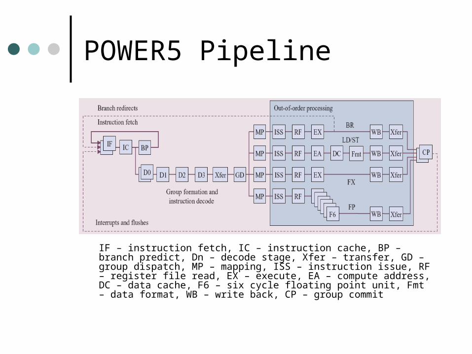
POWER5 Pipeline
IF – instruction fetch, IC – instruction cache, BP – branch predict, Dn – decode stage, Xfer – transfer, GD – group dispatch, MP – mapping, ISS – instruction issue, RF – register file read, EX – execute, EA – compute address, DC – data cache, F6 – six cycle floating point unit, Fmt – data format, WB – write back, CP – group commit

Instruction Data Flow
LSU – load/store unit, FXU – fixed point execution unit, FPU – floating point unit, BXU – branch execution unit, CRL – condition register logical execution unit
Instruction Fetch
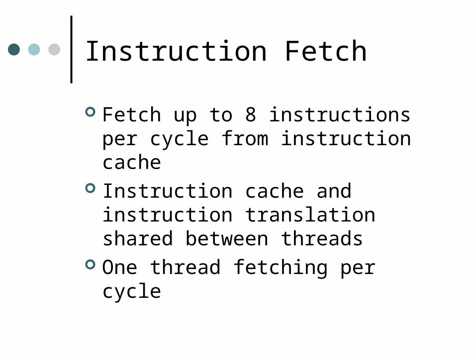
Fetch up to 8 instructions per cycle from instruction cache
Instruction cache and instruction translation shared between threads
One thread fetching per cycle

Branch Prediction
Three branch history tables shared by 2 threads
1 bimodal, 1 path-correlated prediction
1 to predict which of the first 2 is correct
Can predict all branches – even if every instruction fetched is a branch

Branch Prediction
Branch to link register (bclr) and branch to count register targets predicted using return address stack and count cache mechanism
Absolute and relative branch targets computed directly in branch scan function
Branches entered in branch information queue (BIQ) and deallocated in program order
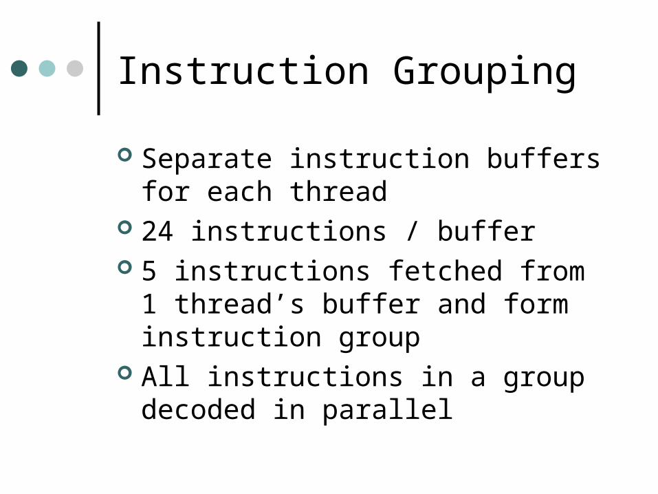
Instruction Grouping
Separate instruction buffers for each thread
24 instructions / buffer 5 instructions fetched from 1 thread’s
buffer and form instruction group All instructions in a group decoded in
parallel

Group Dispatch & Register Renaming
When all resources necessary for group are available, group is dispatched (GD)
D0 – GD: instructions still in program order MP – register renaming, registers mapped to
physical registers Register files shared dynamically by two
threads In ST mode all registers are available to single
thread Placed in shared issue queues

Group Tracking
Instructions tracked as group to simplify tracking logic
Control information placed in global completion table (GCT) at dispatch
Entries allocated in program order, but threads may have intermingled entries
Entries in GCT deallocated when group is committed

Load/Store Reorder Queues
Load reorder queue (LRQ) and store reorder queue (SRQ) maintain program order of loads/stores within a thread
Allow for checking of address conflicts between loads and stores

Instruction Issue
No distinction made between instructions for different threads
No priority difference between threads Independent of GCT group of instruction Up to 8 instructions can issue per cycle Instructions then flow through execution
units and write back stage

Group Commit
Group commit (CP) happens whenall instructions in group have executed
without exceptions and the group is the oldest group in its
thread One group can commit per cycle from
each thread
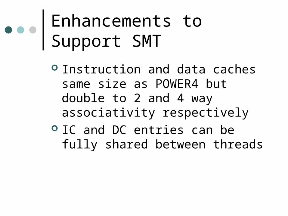
Enhancements to Support SMT
Instruction and data caches same size as POWER4 but double to 2 and 4 way associativity respectively
IC and DC entries can be fully shared between threads

Enhancements to Support SMT Two step address translation
Effective address Virtual Address using 64 entry segment lookaside buffer (SLB)
Virtual address Physical Address using hashed page table, cached in a 1024 entry four way set associative TLB
Two first level translation tables (instruction, data)
SLB and TLB only used in case of first-level miss

Enhancements to Support SMT First Level Data Translation Table – fully
associative 128 entry table First Level Instruction Translation Table
– 2-way set associative 128 entry table Entries in both tables tagged with thread
number and not shared between threads Entries in TLB can be shared between
threads

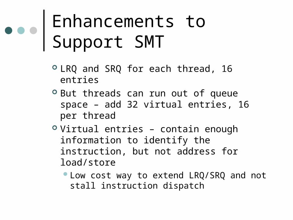
Enhancements to Support SMT LRQ and SRQ for each thread, 16
entries But threads can run out of queue space
– add 32 virtual entries, 16 per thread Virtual entries – contain enough
information to identify the instruction, but not address for load/storeLow cost way to extend LRQ/SRQ and
not stall instruction dispatch

Enhancements to Support SMT Branch Information Queue (BIQ)
16 entries (same as POWER4)Split in half for SMT modePerformance modeling suggested this
was a sufficient solution Load Miss Queue (LMQ)
8 entries (same as POWER4)Added thread bit to allow dynamic
sharing

Enhancements to Support SMT Dynamic Resource Balancing
Resource balancing logic monitors resources (e.g. GCT and LMQ) to determine if one thread exceeds threshold
Offending thread can be throttled back to allow sibling to continue to progress
Methods of throttling• Reduce thread priority (using too many GCT entries)• Inhibit instruction decoding until congestion clears
(incurs too many L2 cache misses)• Flush all thread instructions waiting for dispatch and stop
thread from decoding instructions until congestion clears (executing instruction that takes a long time to complete)

Enhancements to Support SMT
Thread priority Supports 8 levels of
priority 0 not running 1 lowest, 7
highest Give thread with
higher priority additional decode cycles
Both threads at lowest priority power saving mode

Single Threaded Mode
All rename registers, issue queues, LRQ, and SRQ are available to the active threadAllows higher performance than
POWER4 at equivalent frequenciesSoftware can change processor
dynamically between single threaded and SMT mode

RAS of POWER4
High availability in POWER4 Minimize component failure rates Designed using techniques that permit hard
and soft failure detection, recovery, isolation, repair deferral, and component replacement while system is operating
Fault tolerant techniques used for array, logic, storage, and I/O systems
Fault isolation and recovery

RAS of POWER5
Same techniques as POWER4 New emphasis on reducing scheduled outages to
further improve system availability Firmware upgrades on running machine ECC on all system interconnects Single bit interconnect failures dynamically corrected Deferred repair scheduled for persistent failures Source of errors can be determined – for non
recoverable error, system taken down, book containing fault taken offline, system rebooted – no human intervention
Thermal protection sensors

Dynamic Power Management Reduce switching power
Clock gating Reduce leakage power
Minimum low-threshold transistors Low power mode Two stage fix for excess heat
Stage 1: alternate stalls and execution until the chip cools
Stage 2: clock throttling

Effects of dynamic power management with and without simultaneous multithreading enabled. Photographs were taken with a heat-sensitive camera while a prototype POWER5 chip was undergoing tests in the
laboratory.

Memory Subsystem
Memory controller and L3 directory moved on-chip
Interfaces with DDR1 or DDR2 memory
Error correction/detection handled by ECC
Memory scrubbing for “soft errors”Error correction while idle

Cache Sizes
L1 I-cache 64K
L1 D-cache 32K
L2 1.92M
L3 36M

Cache Hierarchy
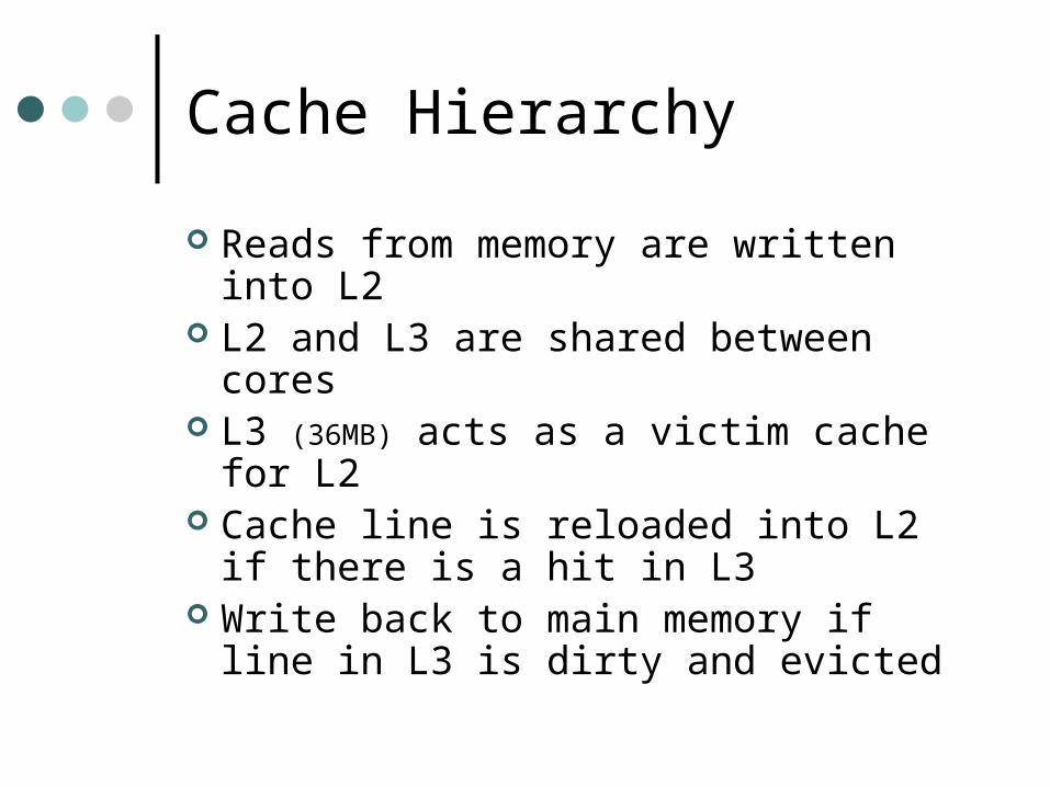
Cache Hierarchy
Reads from memory are written into L2
L2 and L3 are shared between cores L3 (36MB) acts as a victim cache for L2 Cache line is reloaded into L2 if there
is a hit in L3 Write back to main memory if line in
L3 is dirty and evicted

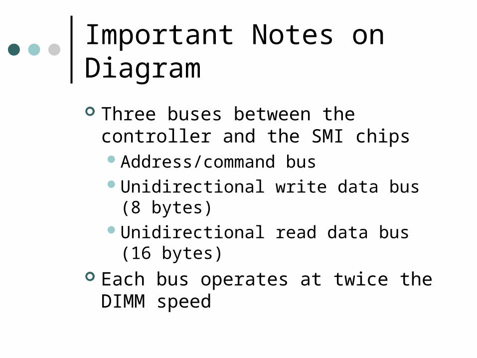
Important Notes on Diagram
Three buses between the controller and the SMI chipsAddress/command busUnidirectional write data bus (8 bytes)Unidirectional read data bus (16
bytes) Each bus operates at twice the DIMM
speed
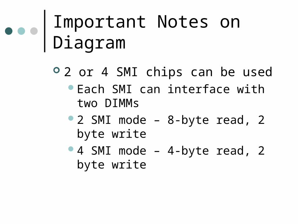
Important Notes on Diagram
2 or 4 SMI chips can be usedEach SMI can interface with two
DIMMs2 SMI mode – 8-byte read, 2 byte
write4 SMI mode – 4-byte read, 2 byte
write

Size does matter
POWER5 Pentium III

…compensating?

Possible configurations
DCM (Dual Chip Module)One POWER5 chip, one L3 chip
MCM (Multi Chip Module)Four POWER5 chips, four L3 chips
Communication is handled by a Fabric Bus Controller (FBC)“distributed switch”

Typical Configurations
2 MCMs to form a “book”
16 way symmetric multi-processor
(appears as 32 way)
DCM books also used

Fabric Bus Controller
“buffers and sequences operations among the L2/L3, the functional units of the memory subsystem, the fabric buses that interconnect POWER5 chips on the MCM, and the fabric buses that interconnect multiple MCMs”
Separate address and data buses to facilitate split transactions
Each transaction tagged to allow for out of order replies

16-way system built with eight dual-chip modules.
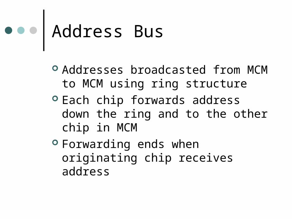
Address Bus
Addresses broadcasted from MCM to MCM using ring structure
Each chip forwards address down the ring and to the other chip in MCM
Forwarding ends when originating chip receives address

Response Bus
Includes coherency information gleaned from memory subsystem “snooping”
One chip in MCM combines other three chips’ snoop responses with the previous MCM snoop response and forwards it on

Response Bus
When originating chip receives the responses, transmits a “combined response” which details actions to be taken
Early combined response mechanism Each MCM determines whether to send a
cache line from L2/L3 depending on previous snoop responses
Reduces cache-to-cache latency

Data Bus
Services all data-only transfers (such as cache interventions)
Services data-portion of address opsCache eviction (“cast-out”)Snoop pushesDMA writes

eFuse Technology
IBM has created a method of morphing processors to increase efficiency
Chips physically alter their design prior to or while functioning
Electromigration, previously a serious liability, is detected and used to determine the best way to improve the chip

The Method
The idea is similar to traffic control on busy highways
A lane can be used for the direction with the most traffic.
So fuses and software algorithm are used to detect circuits that are experiencing various levels of traffic
Method Cont.
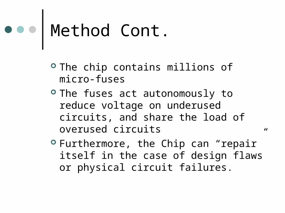
The chip contains millions of micro-fuses
The fuses act autonomously to reduce voltage on underused circuits, and share the load of overused circuits
Furthermore, the Chip can “repair” itself in the case of design flaws or physical circuit failures.

Method Cont.
The idea is not new It has been attempted before,
however previous fuses have affected or damaged the processor

Cons of eFuse
Being able to allocate circuitry throughout a processor implies significant redundancy
Production costs are increased because extra circuitry is required
Over-clocking is countered by the processor automatically detecting a flaw
Pros of eFuse
Significant savings in optimization cost
The need to counter electromigration is no longer as important
The same processor architecture can be altered in the factory, for a more specialized task.
Self-repair and self-upgrading
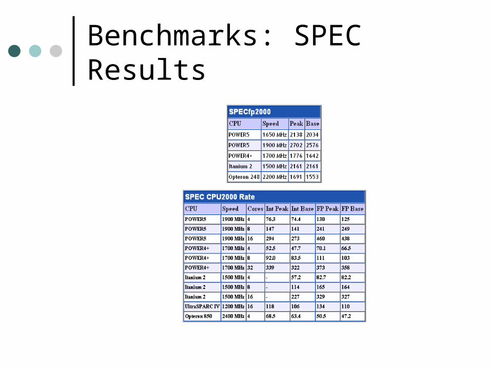
Benchmarks: SPEC Results

Benchmarks

Notes on Benchmarks
IBM’s 64 processor system beat the previous leader (HP’s 64 processor system) by 3x tpmC
IBM’s 32 processor system beat HP’s 64 processor system by about 1.5x
Both of IBM’s systems maintain lower price/tpmC
POWER5 Hypervisor
A hypervisor is the virtualization of a machine allowing multiple operating systems to run on a single system
While the HV is not new, IBM has made many important improvements to the design of HV with the POWER5

Hypervisor Cont.
The main purpose is to abstract the hardware, and divide it logically between tasks
Hardware considerations:Processor timeMemoryI/O

Hypervisor – Processor
The POWER5 hypervisor virtualizes processors
A virtual processor is given to each LPAR
The virtual processor is given a percentage of processing time on one or more processors
Processor time is determined by preset importance values and excess time

HV Processor Cont.
Processor time is defined by processing units, which = 1/100 of a CPU.
A LPAR is given an entitlement in processing units and a weight
Weight is a number between 1 and 256 that implies the importance of the LPAR and its priority in receiving excess PU’s

HV Processor Cont.
Dynamic micro-partitioningThe resources distribution can be further
changed in DLPARThese LPARs are put in the control of PLM
that can actively change their entitlementIn place of a weight, DLPARs are given a
“share” value, that indicates its valueIf a partition is very busy it will be allocated
more PU’s, and vice versa.

Hypervisor – I/O
IBM chose not to give the HV direct control over I/O devices
Instead the HV delegates responsibility of I/O devices to specific LPAR
A LPAR partition serves as a virtual device for the other LPARs on the system
The HV can also give a LPAR sole control over an I/O device.

HV – I/O Cont.
http://www.research.ibm.com/journal/rd/494/armst3.gif

Hypervisor – SCSI
Storage devices are virtualized using SCSI
The hypervisor acts as a messenger from between partitions.
A queue is implemented and the respective partitions is informed of increases in its queue length
The OS running on the controlling partition is in complete control of SCSI execution
Hypervisor – Network
The HV operates a VLAN within its controlled partitions
The VLAN is simplified, secure, and efficient
Each Partition is made aware of a virtual network adaptor
Each partition is labeled with a virtual MAC address and the HV acts as the switch
HV – Network Cont.
However, if the MAC address is unknown to the HV it will deliver the packet to a partition with a physical network adaptor
This partition will deal with external LAN issues such as address translation, synchronization, and packet size

Hypervisor – Console
Virtual Consoles are handled in much the same way.
The Console can also be assigned by the controlling partition as a monitor on an extended network.
The controlling partition can completely simulate the monitors presence through the HV for mundane requirements.