power5 processor and system evolution - · pdf file©2005 ibm power5 processor and system...
TRANSCRIPT

© 2005 IBM
POWER5 Processor and System Evolution
ScicomP 11Charles Grassl
IBMMay, 2005

2 © 2005 IBM Corporation
Agenda
• pSeries systems•Caches•Memory
• POWER5 Processors•Registers•Speeds•Design features

3 © 2005 IBM Corporation
POWER5™ Design
• POWER4 base• Binary and structural compatibility
• Shared memory scalability• Up to 64 processors• 128 threads
• High floating point performance• Server flexibility
• Power efficient design• Utility:
• Reliability, availability, serviceability

4 © 2005 IBM Corporation
POWER5 Systems
• Second generation dual core chip
• Intelligent 2-way SMT• Power management with
no performance impact• 130 nm lithography
• 276M transistors• 8 layers of metal
OS/400OS/400LinuxLinuxLinuxLinuxAIX 5LAIX 5L
POWER HypervisorPOWER HypervisorIOA
AIXkernel
Hardware Management
Console (HMC)
Virtual LANVirtual I/O
LAN IOA
Linuxkernel
Linuxkernel SLIC
LANLAN
IOA IOA LAN IOAIOA
AIX 5LAIX 5L
AIXkernel
Virtual I/OVirtual I/O
Virtual I/O
Integrated xSeries Server
(IXA)
• Micropartitioning• Up to 64 physical
processors,1280 virtual processors per system• Multi Chip Modules
(MCM):• Eight way SMP looks
like 16-way to software• 95 mm on a side

5 © 2005 IBM Corporation
POWER5 System Features
• Dual Core Chip• Shared L2 cache• Shared L3 cache• Shared Memory• Multiple Page Size support• Simultaneous Multi Threading

6 © 2005 IBM Corporation
POWER5 Features
•Chip
Processor 0 Processor 1
L2 L2 L2
0 1 2 3InstructionStreams
L3

7 © 2005 IBM Corporation
POWER4 Chip --- (December 2001)
• Technology: 180nm lithography, Cu, SOI• POWER4+ shipping in 130nm today
• Dual processor core• 8-way superscalar
• Out of Order execution• 2 Load / Store units• 2 Fixed Point units• 2 Floating Point units• Logical operations on Condition
Register• Branch Execution unit
• > 200 instructions in flight• Hardware instruction and data
prefetch L3 D
irect
ory/
Con
trol
L2 L2 L2
LSU LSUIFUBXU
IDU IDU
IFUBXU
FPU FPU
FXU
FXUISU ISU

8 © 2005 IBM Corporation
POWER5 Chip
• IBM CMOS 130nm• Copper and SOI • 8 layers of metal
• Chip• 389 mm2
• 276M transistors• I/Os: 2313 signal, 3057
power• Same technology as
POWER4+

9 © 2005 IBM Corporation
POWER5 Multi-chip Module
• 95mm % 95mm• Four POWER5
chips• Four cache chips• 4,491 signal I/Os• 89 layers of metal

10 © 2005 IBM Corporation
Multi Chip Module (MCM) Architecture
POWER4• 4 processor chips
• 2 processors per chip• 8 off-module L3 chips
• L3 cache is controlled by MCM and logically shared across node
• 4 Memory control chips---------------------------------------• 16 chips
POWER5• 4 processor chips
• 2 processors per chip• 4 L3 cache chips
• L3 cache is used by processor pair
• “Extension” of L2------------------------------------------• 8 chips
L3 ChipMem. Controller

11 © 2005 IBM Corporation
Dynamic Power Management
• Two components:• Switching power• Leakage power
• Impact of SMT on power:• More instructions executed per cycle
• Switching power reduction:• Extensive fine-grain, dynamic clock-gating
• Leakage power reduction• Minimal use of low Vt devices
• No performance impact• Low power mode for low priority threads

12 © 2005 IBM Corporation
Dynamic Power ManagementNo Power Dynamic Power
ManagementManagement
SingleThread
SimultaneousMulti-threading
Photos taken with thermal sensitive camera while
prototype POWER5 chip was undergoing tests
Simultaneous Multi-threading with dynamic power management reduces power consumption below standard, single threaded level

13 © 2005 IBM Corporation
Modifications to POWER4 to create POWER5
P P
L2
Memory
P P
Memory
Mem Ctl Mem Ctl
Fab Ctl Fab Ctl
Reduced L3
Latency
Faster access to memory
L3
L3 Cntrl
L2
L3
L3 Cntrl
Larger SMPs
Larger SMPs
Number of chips cut
in half

14 © 2005 IBM Corporation
64-way SMP Interconnection
Interconnection exploits enhanced distributed switch• All chip interconnections operate at half processor
frequency and scale with processor frequency
8B @ 2:1
IBM Confidential

15 © 2005 IBM Corporation
Simultaneous Multi-Threading in POWER5
• Each chip appears as a 4-way SMP to software
• 2 processors• 2 threads per processor
• Processor resources optimized for enhanced SMT performance
• Software controlled thread priority
• Dynamic feedback of runtime behavior to adjust priority
• Dynamic switching between single and multithreaded mode
Simultaneous Multi-Threading
FX0FX1FP0FP1LS0LS1BRXCRL
Thread 0 active Thread 1 active

16 © 2005 IBM Corporation
Multi-threading Evolution
FX0FX1FP0FP1LS0LS1BRXCRL
Single ThreadFX0FX1FP0FP1LS0LS1BRXCRL
Coarse Grain Threading
FX0FX1FP0FP1LS0LS1BRXCRL
Fine Grain Threading
Thread 1 Executing
Thread 0 Executing
No Thread Executing
FX0FX1FP0FP1LS0LS1BRXCRL
Simultaneous Multi-Threading

17 © 2005 IBM Corporation
Simultaneous multi-threading
POWER4 (Single Threaded)POWER5 Simultaneous Multi Threading
Syst
emth
roug
hput
• Utilizes unused execution unit cycles• Symmetric multiprocessing (SMP) programming model • Natural fit with superscalar out-of-order execution core• Dispatch two threads per processor. Net result:
• Better processor utilization
CRL
FX0FX1LSOLS1FP0FP1BRZ
Thread1 active
Thread0 activeNo thread active
SMTST
Appears as 4 CPUs per chip to the
operating system (AIX 5L V5.3 and
Linux)

18 © 2005 IBM Corporation
POWER5 Performance Expectations
• Higher sustained-to-peak floating point rate ratio compared to POWER4
• Reduction in L3 and memory latency• Integrated memory controller
• Increased rename resources• Higher instruction level parallelism in compute
intensive applications
• Fast barrier synchronization operation• Enhanced data prefetch mechanism

19 © 2005 IBM Corporation
Processor Architecture
• CPUs• Caches• Performance Features

20 © 2005 IBM Corporation
Chip Enhancements
• Caches and translation resources• Larger caches• Enhance associativity
• Resource pools• Rename registers: GPRs, FPRs increased to 120 each• L2 cache coherency engines: increased by 100%
• Memory controller moved on chip• Dynamic power management
21 © 2005 IBM Corporation
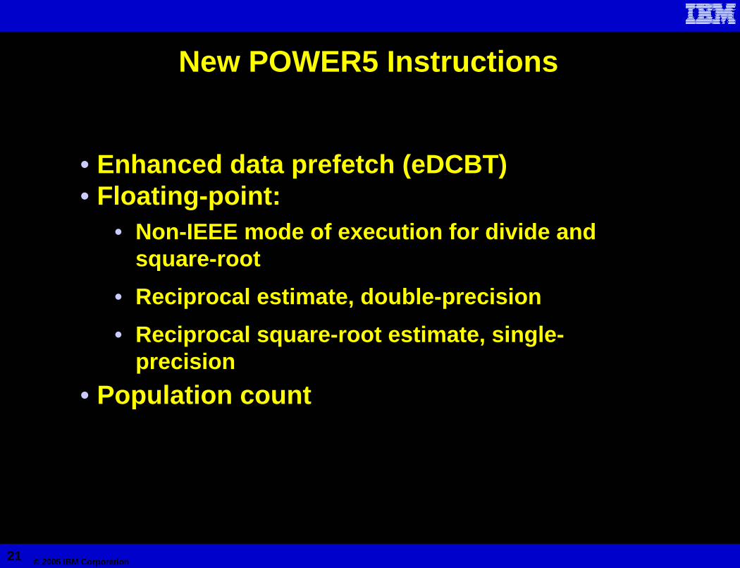
New POWER5 Instructions
• Enhanced data prefetch (eDCBT)• Floating-point:
• Non-IEEE mode of execution for divide and square-root
• Reciprocal estimate, double-precision• Reciprocal square-root estimate, single-
precision• Population count

22 © 2005 IBM Corporation
Processor Characteristics
• Deep pipelines• High frequency clocks• High asymptotic rates• Superscalar• Speculative out-of-order instructions • Up to 8 outstanding cache line misses• Large number of instructions in flight• Branch prediction• Prefetching

23 © 2005 IBM Corporation
POWER4 and POWER5 Storage HierarchyPOWER4 POWER5
L2 Cache
Capacity, line size 1.44 Mbyte128 byte line
1.92 Mbyte128 byte line
Associativity, replacement 8-way, LRU 10-way, LRU
Type Distributed switch Enhanced distributed switch
Intra-MCM data buses ½ processor speed Processor speed
Off-chip L3 Cache
Capacity, line size 32 Mbyte512 byte line
36 Mbyte256 byte line
Associativity, replacement 8-way, LRU 12-way, LRU
Chip interconnect
Inter-MCM data buses 1/3 processor speed ½ processor speedMemory 1 Tbyte 2 Tbyte
IBM Confidential
24 © 2005 IBM Corporation
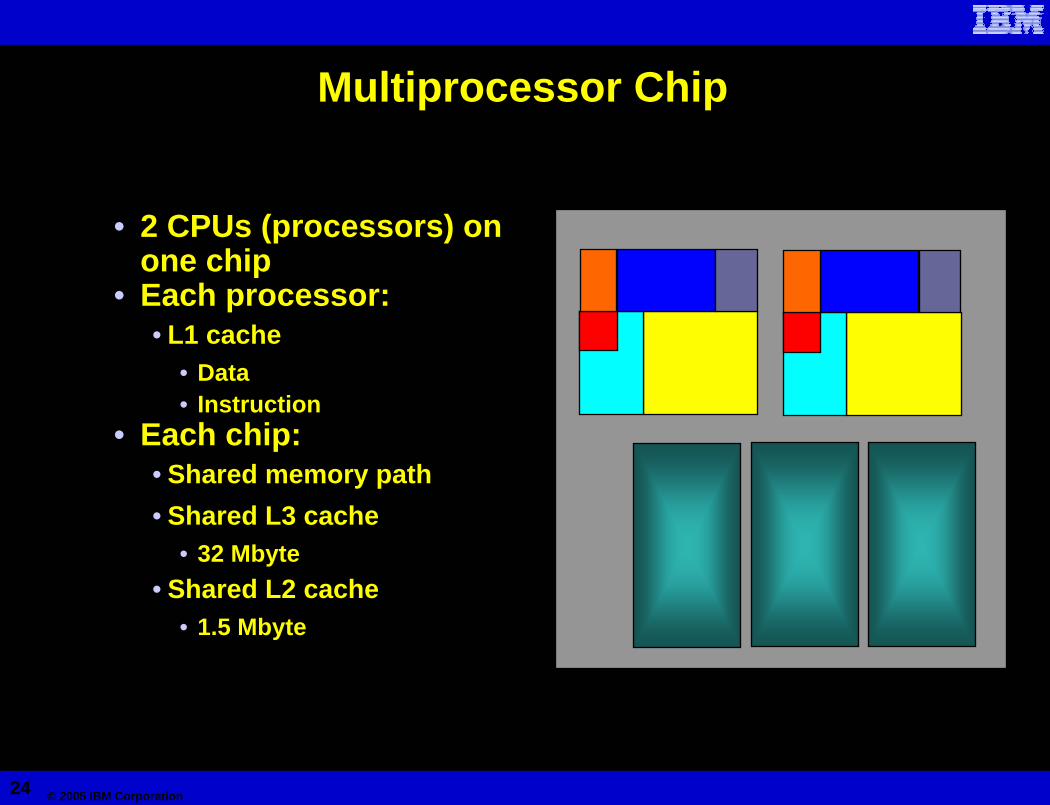
Multiprocessor Chip
• 2 CPUs (processors) on one chip
• Each processor:• L1 cache
• Data• Instruction
• Each chip:• Shared memory path• Shared L3 cache
• 32 Mbyte• Shared L2 cache
• 1.5 Mbyte

25 © 2005 IBM Corporation
Chip Structure
L2Cache
L2Cache
L2Cache
ProcessorCore 1
ProcessorCore 1
Fabric ControllerMCM
ToMCM
MCMTo
MCM
ChipTo
Chip
ChipTo
Chip
L3 Directory
GX Bus L3/MemBus
GX Control L3/Mem Control

26 © 2005 IBM Corporation
Micro Architecture
• 64-bit RISC Microprocessor• Multiple Execution Units• Hardware Data Prefetch• Out-of-Order Execution• Speculative Execution• 8 Instructions / Cycle

27 © 2005 IBM Corporation
Multiple Functional Units
• Symmetric functional units• Two Floating Point Units (FPU)• Three Fixed Point Units (FXU)
• Two Integer• One Control
• Two Load/Store Units (LSU)• One Branch Processing Unit (BPU)
Branch
FMA
FMA
Fixed Pt.
Fixed Pt.
•CR
Load/Store
Load/Store

28 © 2005 IBM Corporation
Fast Core: Instruction-level Parallelism• Speculative superscalar
organization• Out-of-Order execution• Large rename pools• 8 instruction issue, 5 instruction
complete• Large instruction window for
scheduling• 8 Execution pipelines
• 2 load / store units• 2 fixed point units• 2 DP multiply-add execution units• 1 branch resolution unit• 1 CR execution unit
• Aggressive branch prediction• Target address and outcome
prediction• Static prediction / branch hints used• Fast, selective flush on branch
mispredict
FX1ExecUnit
FX2ExecUnit
FP1ExecUnit
FP2ExecUnit
CRExecUnit
BRExecUnit
BR/CRIssue Q
FX/LD 1Issue Q
FX/LD 2Issue Q
FPIssue Q
D-cache
StQ
LD2ExecUnit
LD1ExecUnit
Decode,Crack &Group
Formation
Instr Q
IFARI-cache
GCT
BRScan
BRPredict
Processor Core

29 © 2005 IBM Corporation
Registers
Resource Logical POWER4: Physical
POWER5: Physical
80 120120
32
16
20
24
7232
16
20
24
GPRs 32FPRs 32
CRs 8 (9) 4-bit fields
Link/Count 2
FPSCR 1
XER 4 fields

30 © 2005 IBM Corporation
Functional Unit Progression
POWER2:
POWER3:
POWER4:
POWER2 POWER3 POWER4 POWER5Clock Periods 2 3 6
1.3 GHz
4.6
Clock Rate 125 MHz 375 MHz6
1.9 GHzTime (Nanosec.) 16 8 3.2

31 © 2005 IBM Corporation
Registers
• CPU's point of view•120 FP registers (POWER5)
• User point of view•32 FP registers (architecture)
• Rename registers•Relieve register "pressure"
32 Architecture Registers 72 Physical Registers

32 © 2005 IBM Corporation
Register Renaming
• Architecture has 32 registers•Legacy
• Cases which require additional registers:•Tight loops
• Computationally intensive•“Broad” loops
• Many variables involved•Deep pipe lines
• Renaming registers are increasingly important with Simultaneous MultiThreading

33 © 2005 IBM Corporation
Register Renaming:Read After Write
Nothing to be done
R13 = R14 + R15
…R16 = R13 + R12

34 © 2005 IBM Corporation
Register Renaming:Write After Write
R13 = R14 + R15
…R13 = R16 + R17
R19 = R13 + R18
R13 = R14 + R15
…R42 = R16 + R17
R19 = R42 + R18
Renaming

35 © 2005 IBM Corporation
Effect of Registers
POWER4 POWER5
GP Registers 80 120
FP Registers 72 120
DGEMM speed 60% of burst 90% of burst
Enhances performance ofcomputationally intensive kernels

36 © 2005 IBM Corporation
Renaming Example
• Matrix multiple with 4x unrolling•2 FMAs and 1 LFD per cycle•3 renames per cycle•After 13 cycles, 39 FP renames of the 40 (POWER4, 72-32) are allocated
•Cycles 14, 16, and 18:• Instruction are rejected due to lack of renames
• Result: ~70 to 75% of peak•Software rule of thumb:•approx. 13 renames available every 6 cycles
• POWER5 alleviates this with 120 FP renames

37 © 2005 IBM Corporation
Effect of Rename Registers
0
1000
2000
3000
4000
5000
6000
7000
POWER4 POWER5
Mflo
p/s
PeakMATMUL
0
1000
2000
3000
4000
5000
6000
7000
POWER4 POWER5
Mflo
p/s
PeakPolynomial
POWER4 @ 1.5 GHz POWER5 @ 1.65 GHz

38 © 2005 IBM Corporation
Floating Point Functional Units
• Two floating point execution units• Divide and square root sub-
units• NOT pipelined• Double precision (64-bit) data
path Instruction Single(Cycles)
Double(Cycles)
Fma 6 6
Fdiv ~25 32
Fsqrt - 34

39 © 2005 IBM Corporation
Floating Point Functional Units
• 2 floating add-multiply (FMA) units•Per instruction:
• 1 floating point add• 1 floating point multiply
•4 floating point ops per clock period• IEEE arithmetic

40 © 2005 IBM Corporation
Arithmetic
Size Integer FloatingPoint
16 Yes No
32 Yes Yes
64 Yes(-q64) Yes
128 No No
• IEEE 754 single and double floating-point
• Floating multiply-add:• Intermediate value is not rounded
• 64-bit integer arithmetic instructions• Used only in 64-bit addressing mode

41 © 2005 IBM Corporation
Pipelined Functional Units
Multiply AddMultiply or Add 12 results/
6 clock periods
Divide 2 results/32 clock periods
Square root 2 results/34 clock periods
A,B, C A*B+C
D, E, F D*E+F
DivideA/BA,B
D/ED, E

42 © 2005 IBM Corporation
Deep Pipelines
• Operations limited by functional unit transit time:•Divide•Square root• Intrinsic functions•Recursion

43 © 2005 IBM Corporation
Translation Lookaside Buffer (TLB)
• 1024 entry• Page sizes:• 4096 Bytes• 16 Mbyte
Address Page
Memory
Page
PagePage
Page Page

44 © 2005 IBM Corporation
TLB Thrashing
• TLB spans a small amount of memory• Strategy:
•Avoid large strides•Avoid randomly using large constructs•Gather and scatter are very bad
• Common problem on RISC microprocessors

45 © 2005 IBM Corporation
Hardware Prefetch
• Detects adjacent cache line references• Forward and backward strides• Prefetches up to two lines ahead per stream
• Up to eight concurrent streams• Twelve prefetch filter queues• No prefetch on store misses
• (when a store instruction causes a cache line miss)• Ramped Initialization
• L2 to L1 prefetches• L3 to L2 prefetches• Memory to L3 prefetches

46 © 2005 IBM Corporation
Memory Access
• Load and Store• Two per CPU• Connect CPU to memory
MemoryPrefetchBuffers
MemoryProcessorLoad Store
Load Store

47 © 2005 IBM Corporation
Memory Prefetching
• Eight prefetch stream buffers• Connect CPU to memory
Stream 7
Stream 8
Stream 1
Stream 2
MemoryProcessorLoad Store
Load Store
Prefetch Buffers

48 © 2005 IBM Corporation
Cache Line Load
• Memory system does not detect patterns within cache line
• Detect location within first 3/4 or last 1/4 of cache line

49 © 2005 IBM Corporation
Stride Pattern Recognition
• Upon a cache miss:•Biased guess is made as to the direction of that stream
•Guess is based upon where in the cache line the address associated with that miss occurred
• If it is in the first 3/4, then the direction is guessed as ascending
• If in the last 1/4, the direction is guessed descending

50 © 2005 IBM Corporation
Prefetching
Memory
1
2
3
4
1 2 3 4 5 6
5
6
7
8
Cache Lines

51 © 2005 IBM Corporation
Streams
Memory Processor Non-Streaming
Memory ProcessorStreaming

52 © 2005 IBM Corporation
Streams
Memory Processor

53 © 2005 IBM Corporation
Effect of Prefetch Buffers
• Memory load overlap• Up to 8 streams• Variables• Patterns
Six streams:1 A4 B's1 C
for (j=0;j<m;j++)for (i=0;i<n;i++)
A[j][i] = A[j][i]+s0*B[j+0][i] +s1*B[j+1][i]+s2*B[j+2][i]+s3*B[j+3][i]+C[i]

54 © 2005 IBM Corporation
Memory Bandwidth
0
2000
4000
6000
8000
10000
12000
Mby
te/s
ESSL DCBZ Copy Daxpy Daxpy2 Daxpy4
LPSP
p5-595 1.9 GHz

55 © 2005 IBM Corporation
Memory Bandwidth
0
2000
4000
6000
8000
10000
12000
Mby
te/s
ESSL
DC
BZ
Cop
y
Dax
py
Dax
py2
Dax
py4
POWER5 LPPOWER5 SPPOWER4 SP
p5-595 1.9 GHzp690 1.3 GHz

56 © 2005 IBM Corporation
Memory Bandwidth
0
2000
4000
6000
8000
10000
12000• Typical POWER5 bandwidth:• 4 Gbyte/s Small Pages (SP)• 8 Gbyte/s Large pages (LP)• Twice the bandwidth of
POWER4

57 © 2005 IBM Corporation
Memory Bandwidth: Stream Buffers
01000200030004000500060007000
Mby
te/s
1 2 3 4 5 6 7 8 9 10 11 12Right Hand Sides
LPSP
p5-595 1.9 GHz

58 © 2005 IBM Corporation
Strides
Bandwidth Reduction
Stride Single Double1 1x 1x2 ½ ½4 ¼ ¼8 1/8 1/816 1/16 1/1632 1/32 1/1664 1/32 1/16
• Cache line size is 128 bytes• Double precision: 16 words• Single precision: 32 words

59 © 2005 IBM Corporation
Stride Test:Small Strides
0100020003000400050006000700080009000
Mby
te/s
-16 -12 -10 -8 -6 -4 -2 -1 1 2 4 6 8 10 12 16
Stride (Double Precision)
p5-595 1.9 GHz

60 © 2005 IBM Corporation
Stride Test:Large Strides
050
100150200250300350400450
Mby
te/s
24 32 36 68 132 260 516 1028Stride (Double Precision)
LPSP
p5-595 1.9 GHz

61 © 2005 IBM Corporation
POWER5: Memory
• One or two memory cards per MCM•Best bandwidth with two memory cards
• 16 Gbyte/s bandwidth per chip
L3
L3
L3 L3

62 © 2005 IBM Corporation
Interleaved Memory
• Interleaved 4 way within MCM • (Only if 2 memory cards match in size)
• Pages interleaved within an MCM
• Consecutive pages can be on any MCM
L3
L3
L3 L3

63 © 2005 IBM Corporation
Memory Page Placement
• Default is random page placement•Small pages
• Local page placement optional with "first touch" policy
• "Round robin" option available with AIX 5.2• Large pages are also available
•Loader option or "tag" binary•Large pages are statically allocated•Placed at allocation time, not first reference

64 © 2005 IBM Corporation
Memory Allocation
• Pages are allocated by module• Approximately uniform distribution• Approximately round robin

65 © 2005 IBM Corporation
Memory Allocation
• Memory Affinity•Allocate pages on memory local to module

66 © 2005 IBM Corporation
Memory Latencies:POWER4 and POWER5
Time vs. Length
050
100150200250300
0 500000000 1000000000Length
Nan
osec
onds
POWER5 MCMPOWER4
p655 1.5 GHzp5-595 1.9 GHz

67 © 2005 IBM Corporation
Memory Latencies:POWER5 Memory Affinity
Time vs. Length
050
100150200250300
0 500000000 1000000000Length
Nan
osec
onds
POWER5POWER5 MCM
p655 1.5 GHzp5-595 1.9 GHz

68 © 2005 IBM Corporation
Memory Latencies:L1 Cache – L2 Cache
Time vs. Length
02468
10
0 20000 40000 60000Length
Nan
osec
onds
p5-595 1.9 GHz

69 © 2005 IBM Corporation
Memory Latencies:L3 cache - Memory
Time vs. Length
050
100150200250
0 50000000 100000000Length
Nan
osec
onds
p5-595 1.9 GHz

70 © 2005 IBM Corporation
Memory Latencies
Region Size(byte)
Time(nanosec.)
Clocks (1.9 GHz)
L1 32 kbyte
36 Mbyte
L3 36 Mbyte 48 92
Memory - 210 403
1 2
L2 9 32
p5-595 1.9 GHzProgram: Lmbench

71 © 2005 IBM Corporation
Memory Latency
Level POWER4 POWER4+ POWER5
L1 2 2
7
75
255
L2 9
2
9
48L3 95
Memory 295 210
Results are in nanoseconds

72 © 2005 IBM Corporation
Chip to Chip Communications
• On chip•2:1 bus frequency
• Bandwidth• 35 Gbyte/s

73 © 2005 IBM Corporation
Memory Performance
• Bandwidth•3 – 8 Gbyte/s per single processor•200 Gbyte/s per p5-595
• Latency•~200 nanoseconds
74 © 2005 IBM Corporation
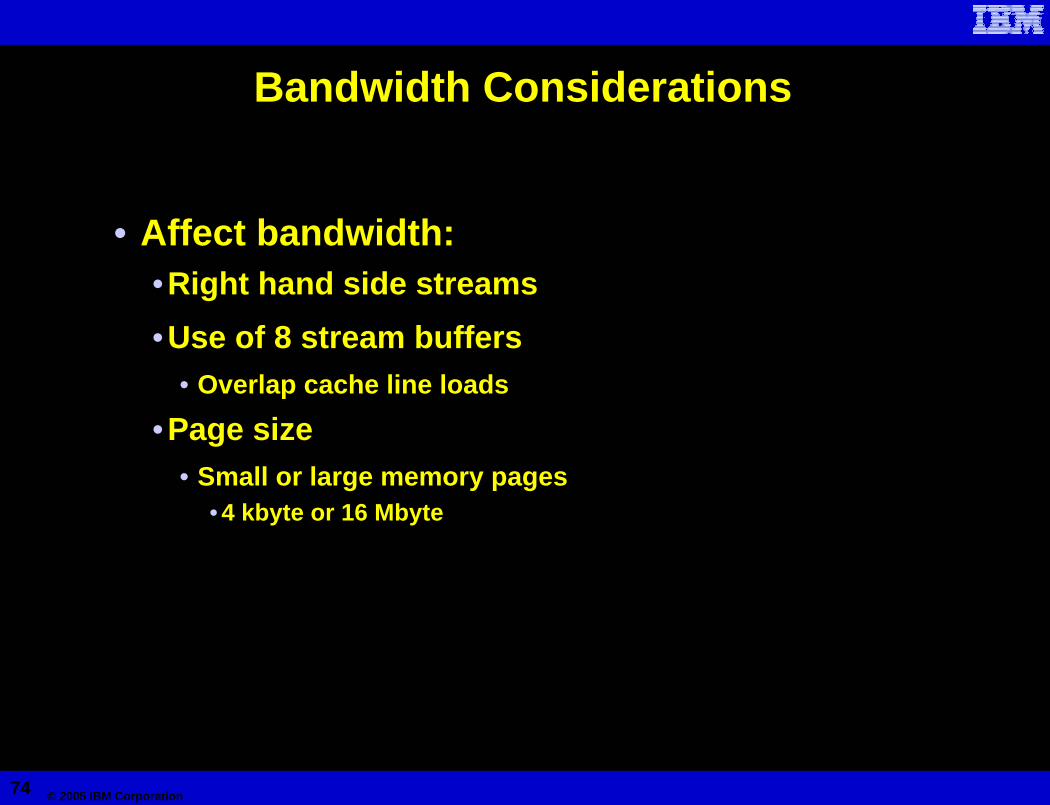
Bandwidth Considerations
• Affect bandwidth:•Right hand side streams•Use of 8 stream buffers
• Overlap cache line loads
•Page size• Small or large memory pages
• 4 kbyte or 16 Mbyte

75 © 2005 IBM Corporation
Summary
• POWER5•8 Functional units
• Chip:•2 processors•Shared L2 cache
• Module•Four chips•8 processors
• P5-595 system•8 Modules

76 © 2005 IBM Corporation
Summary
• Registers:• 32 architecture• 88 rename
• Functional Units• 6 clock periods for FMA
• Pipelined• 32 clock periods for FDIV
• NOT pipelined• 1024 entry TLB• 4096 byte page• 8 prefetch streams