powertip ph480272t006-ibb tft-display distributed by data modul … · (1) keep the gap, for...
TRANSCRIPT

TECH. CORP.
SPECIFICATIONS
CUSTOMER : PTC
SAMPLE CODE : SH480272T006-IBB
MASS PRODUCTION CODE : PH480272T006-IBB
SAMPLE VERSION : 01
SPECIFICATIONS EDITION : 006
DRAWING NO. (Ver.) : JLMD- PH480272T006-IBB_004
PACKAGING NO. (Ver.) : JPKG- PH480272T006-IBB_001
Customer Approved
Date:
Approved Checked Designer
閆偉 劉進 陳璐
□ Preliminary specification for design input
■ Specification for sample approval
POWERTIP TECH. CORP.
Headquarters: No.8, 6th Road, Taichung Industrial Park,
Taichung, Taiwan
台中市 407工業區六路 8號
TEL: 886-4-2355-8168
FAX: 886-4-2355-8166
E-mail: [email protected]
Http://www.powertip.com.tw
NO.PT-A-005-8
P O W E R T IP
JS R D A P P R O V E D
2017.07.24

SH480272T006-IBB Page2 SAMPLE Ver.01 SPEC Edi.006
History of Version
Date (mm / dd / yyyy)
Ver. Edi. Description Page Design by
07/16/2012 01 001 New Drawing. - 李誠
09/17/2013 01 002 New Sample - 李誠
04/08/2014 01 003 Add FPC suggested connector Appendix 李誠
08/14/2015 01 004 Modify BL Life Time 11 周志仙
11/09/2016 01 005 Update LCM Drawing Appendix 陳璐
07/21/2017 01 006 Modify Touch Panel Characteristics 12~15 陳璐
Total: 32 Page
SH480272T006-IBB Page3 SAMPLE Ver.01 SPEC Edi.006
Contents
1. SPECIFICATIONS 1.1 Features 1.2 Mechanical Specifications 1.3 Absolute Maximum Ratings 1.4 DC Electrical Characteristics 1.5 Optical Characteristics 1.6 Backlight Characteristics 1.7 Touch Panel Characteristics
2. MODULE STRUCTURE 2.1 Counter Drawing 2.2 Interface Pin Description 2.3 Timing Characteristics 2.4 Data Format 2.5 Power On/Off Sequence
3. QUALITY ASSURANCE SYSTEM 3.1 Quality Assurance Flow Chart 3.2 Inspection Specification
4. RELIABILITY TEST 4.1 Reliability Test Condition
5. PRECAUTION RELATING PRODUCT HANDLING 5.1 Safety 5.2 Handling 5.3 Storage 5.4 Terms of Warranty
Appendix:LCM Drawing
Packaging

SH480272T006-IBB Page4 SAMPLE Ver.01 SPEC Edi.006
1. SPECIFICATIONS
1.1 Features
Item Standard Value
Display Type 480 * 3 (RGB) * 272 Dots
LCD Type a-Si TFT , Normally white, Transmissive type
Screen size(inch) 4.3 inch
Viewing Direction 6 O’clock
Color configuration RGB-Strip
Interface Digital 24-bits RGB
Other(controller/driver
IC)
OTA5180A
(Or Compatible IC )
ROHS
THIS PRODUCT CONFORMS THE ROHS OF PTC
Detail information please refer web site :
http://www.powertip.com.tw/news.php?area_id_view=1085560481/
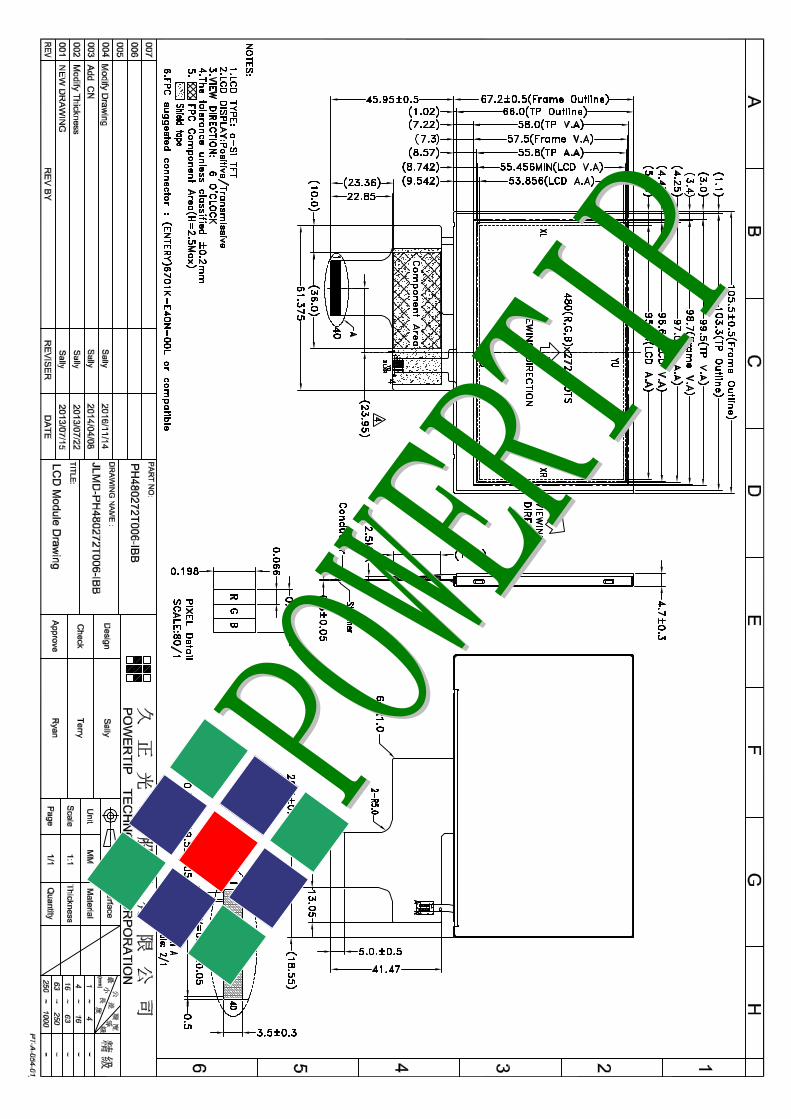
1.2 Mechanical Specifications
Item Standard Value Unit
Outline Dimension 105.5(W) x 67.2 (L) x 4.7(H) mm
LCD panel
Item Standard Value Unit
Active Area 95.04 (W) x 53.856 (L) mm
Touch panel
Item Standard Value Unit
Viewing Area 99.5 (W) * 58.0 (L) mm
Active Area 97.0 (W) * 55.8 (L) mm
Note : For detailed information please refer to LCM drawing
SH480272T006-IBB Page5 SAMPLE Ver.01 SPEC Edi.006
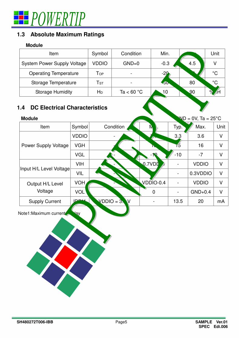
1.3 Absolute Maximum Ratings
Module
Item Symbol Condition Min. Max. Unit
System Power Supply Voltage VDDIO GND=0 -0.3 4.5 V
Operating Temperature TOP - -20 70 °C
Storage Temperature TST - -30 80 °C
Storage Humidity HD Ta < 60 °C 10 90 %RH
1.4 DC Electrical Characteristics
Module GND = 0V, Ta = 25°C
Item Symbol Condition Min. Typ. Max. Unit
Power Supply Voltage
VDDIO - 3.0 3.3 3.6 V
VGH - 13 15 16 V
VGL - -10 -10 -7 V
Input H/L Level Voltage VIH - 0.7VDDIO - VDDIO V
VIL - 0 - 0.3VDDIO V
Output H/L Level
Voltage
VOH - VDDIO-0.4 - VDDIO V
VOL - 0 - GND+0.4 V
Supply Current IDD*1 VDDIO = 3.3 V - 13.5 20 mA
Note1:Maximum current display

SH480272T006-IBB Page6 SAMPLE Ver.01 SPEC Edi.006
1.5 Optical Characteristics TFT LCD Module VDDIO= 3.3 V, Ta=25°C
Item Symbol Condition Min. Typ. Max. unit -
Response time Tr+Tf 25℃ - - 30 45 ms Note2
Viewing angle
Rear Θ+
CR ≥ 10
- 60 -
Deg. Note 1 Front Θ- - 60 -
Left ΘL - 60 -
Right ΘR - 60 -
Contrast ratio CR - 500 600 - - Note 3
Color of CIE Coordinate
(With B/L&T/P)
White X
IF= 20 mA
0.26 0.31 0.36
- Note 4
Y 0.30 0.35 0.40
Red X 0.55 0.60 0.70
Y 0.29 0.34 0.39
Green X 0.29 0.34 0.39
Y 0.57 0.62 0.67
Blue X 0.11 0.16 0.21
Y 0.08 0.13 0.18
Average Brightness
Pattern=white display
(With LCD&T/P)
IV IF= 20 mA 400 500 - cd/m2 Note 4
Uniformity
(With LCD&T/P) △B - 80 - - % Note 4
Note 4 :
1:△B=B(min) / B(max) * 100%
2:Measurement Condition for Optical Characteristics:
a:Environment: 25 ±5℃ ℃ / 60±20%R.H,no wind,dark room below 10 Lux at typical lamp
current and typical operating frequency.
b:Measurement Distance: 500 ± 50 ㎜ ,(θ= 0°)
c:Equipment: TOPCON BM-7 fast,(field 1°),after 10 minutes operation.
d:The uncertainty of the C.I.E coordinate measurement ±0.01,Average Brightness ± 4%
1 2 3
6 5 4
7 8 9
VIEW AREA
LCM
θ θ
Colorimeter=BM-7 fast
500㎜

SH480272T006-IBB Page7 SAMPLE Ver.01 SPEC Edi.006
Note 1.
Optical characteristics-2
Viewing angle
Front (6H)
φ=270°
Rear (12H)
φ=90°
Right (3H)
φ=0°
Left (9H)
φ=180°
θL
Viewing angle
Top (θ=0°)
θR
θ-
θ+
SH480272T006-IBB Page8 SAMPLE Ver.01 SPEC Edi.006
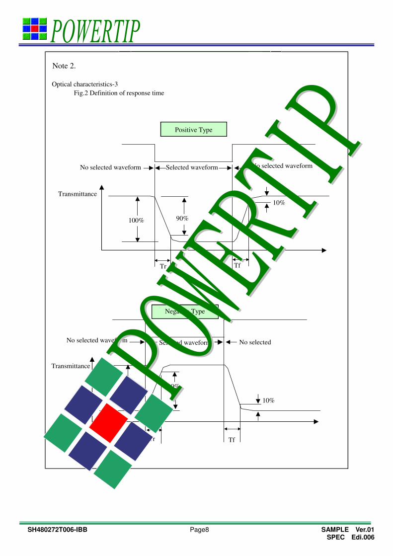
Note 2.
Optical characteristics-3
Fig.2 Definition of response time
Positive Type
Selected waveformNo selected waveform No selected waveform
100% 90%
10%
TfTr
Transmittance
Negative Type
100% 90%
10%
TfTr
No selected Selected waveformNo selected waveform
Transmittance
SH480272T006-IBB Page9 SAMPLE Ver.01 SPEC Edi.006
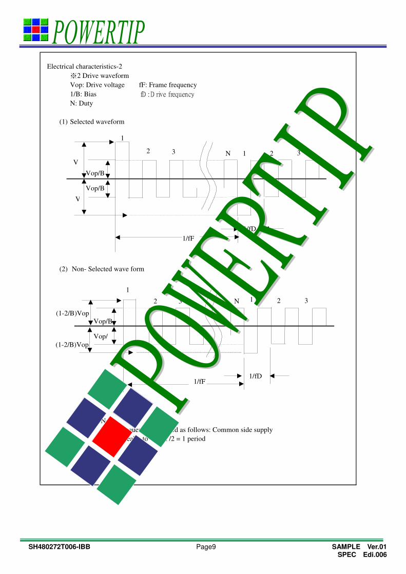
Electrical characteristics-2
※2 Drive waveform
Vop: Drive voltage fF: Frame frequency
1/B: Bias fD : D rive frequency
N: Duty
(1) Selected waveform
(2) Non- Selected wave form
1
V
o
Vop/B
Vop/B
V
1/fF
1/fD
32N32
1
Note:
Frame frequency is defined as follows: Common side supply
voltage peak - to - peak /2 = 1 period
Vop/
1/fF1/fD
321N32
1
(1-2/B)Vop
Vop/B
(1-2/B)Vop

SH480272T006-IBB Page10 SAMPLE Ver.01 SPEC Edi.006
Note 3. : Definition of Vth
Active voltage range
View direction
Drive waveform
Transmittance
※1 Contrast ratio
= (Brightness in OFF state) / (Brightness in ON state)
Outline of Electro-Optical Characteristics Measuring System
Measuring System: Autronic DMS-803
50%
(No selected waveform)
73%
Vth2
40°
(Selected waveform)
Vth1
10°
Selected waveform
No selected waveform
DriveVth2Vth1
Transmittance
100
73%
50%
θ
ψ
Human
Photo Detector
LCD PanelTransmissive
Temperatur
e Control
Chamber
Active

SH480272T006-IBB Page11 SAMPLE Ver.01 SPEC Edi.006
1.6 Backlight Characteristics
Maximum Ratings
Item Symbol Conditions Min. Max. Unit
LED Forward Current IF Ta =25℃ - 30 mA
LED Reverse Voltage VR Ta =25℃ - 1.0 V
Power Dissipation PD Ta =25℃ - 735 mW
Electrical / Optical Characteristics
Item Symbol Conditions Min. Typ. Max. Unit
Forward Voltage VF
IF= 20mA
18.2 22.8 24.5 V
Average Brightness
(Without LCD &T/P) IV 5500 6000 - cd/m2
CIE Color Coordinate
(Without LCD &T/P)
X 0.26 0.30 0.33 -
Y 0.26 0.30 0.33
Color White
Circuit diagram:
Other Description
Item Conditions Description
Life Time Ta =25℃
IF= 20 mA 20000 hrs
SH480272T006-IBB Page12 SAMPLE Ver.01 SPEC Edi.006
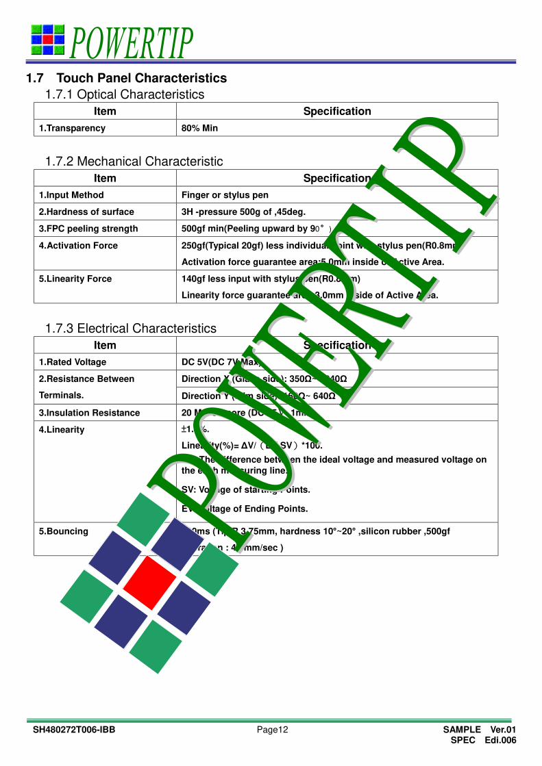
1.7 Touch Panel Characteristics
1.7.1 Optical Characteristics
Item Specification
1.Transparency 80% Min
1.7.2 Mechanical Characteristic
Item Specification
1.Input Method Finger or stylus pen
2.Hardness of surface 3H -pressure 500g of ,45deg.
3.FPC peeling strength 500gf min(Peeling upward by 90°)
4.Activation Force 250gf(Typical 20gf) less individual point with stylus pen(R0.8mm)
Activation force guarantee area:5.0mm inside of Active Area.
5.Linearity Force 140gf less input with stylus pen(R0.8mm)
Linearity force guarantee area:3.0mm inside of Active Area.
1.7.3 Electrical Characteristics
Item Specification
1.Rated Voltage DC 5V(DC 7V Max)
2.Resistance Between
Terminals.
Direction X (Glass side): 350Ω~ 1240Ω
Direction Y (Film side): 160Ω~ 640Ω
3.Insulation Resistance 20 MΩ or more (DC 25Ⅴ 1min)
4.Linearity ±1.5%.
Linearity(%)= ΔV/(EV-SV)*100.
ΔV: The difference between the ideal voltage and measured voltage on
the each measuring line.
SV: Voltage of starting Points.
EV: Voltage of Ending Points.
5.Bouncing <10ms (Tip R 3.75mm, hardness 10°~20° ,silicon rubber ,500gf
operation : 40 mm/sec )

SH480272T006-IBB Page13 SAMPLE Ver.01 SPEC Edi.006
1.7.4 Reliability Characteristic
Item Specification
1.Hitting Durability 1,000,000times min.( Tip R 8mm&R0.8mm)
2.Pen Sliding Durability 100,000 times min(Tip R0.8mm).
3.Impact Resistance No damage when ψ9mm steel ball is dropped on the surface from 30 cm
height at 1 time.
4.Flexible pattern Bending
Resistance
Bending 3 times by bending radius R1.0 mm
5.Flexible Pattern Insert/Pull
Out Resistance 5times at least .

SH480272T006-IBB Page14 SAMPLE Ver.01 SPEC Edi.006
1.7.5 Touch Panel Design/Handing Guide
(1) Keep the gap, for example 0.2 to 0.3mm, between bezel edge and T/P edge.
The reason is to avoid the bezel edge from contacting T/P surface that may cause “short” with
bottom layer
(2) Insertion a cushion material is recommended.
(3) The cushion material should be limited on the busbar insulation paste area. If it is over the
transparent insulation paste area, a “short” may be occurred.
(4) Do not to use an adhesive tape to bond it on the front of T/P and hang it to the housing bezel.
(5) Never expand the T/P top layer (PET Film) like a balloon by internal air pressure. The life of the T/P
will extremely decreasing.
(6) Top layer, PET, dimension is changing base on environment temperature and humidity. Please
avoid a stress from housing bezel to top layer, because it may cause “waving”.
(7) The input to the Touch Panel sometimes distorts touch panel itself.
(8)To use the stylus pen or fingernail sliding at the edge of the housing is prohibited. It would cause
the cracking of the ITO coating and damage the touch panel. It also request not to press this area
while assembling
(9) Purpose: In order to prevent accidental use and performance deterioration, please keep the
following precautions.
In order to prevent unusual performance degradation and malfunction of a touch panel, please carry
out the set case designing and a touch panel assembling method after surely considering the
definition of each area illustrated in above figure.

SH480272T006-IBB Page15 SAMPLE Ver.01 SPEC Edi.006
Area(a):Active area
The active area is guaranteed the position data detectable precision, operation force and other
operations. it is strongly recommended to place the operation button or menu keys within the active
area. Due to structure, the active area is less durable at the edge or close to the edge.
Area(b):Operation non-guaranteed area
This area does not guarantee a touch panel operation and its function. When this area is pressed,
touch panel shows degradation of its performance and durability such as a pen sliding durability
becomes about one-tenth compared with the active area (area-(a) as guaranteed area) and its
operation force requires about double. About 0.5 mm outside from a boundary of the active area
corresponds to this area.
Area(c):Pressing prohibition area
The area which forbids pressing, because an excessive load is applied to a transparent electrode (ITO)
and a serious damage is given to a touch panel function by pressing. About 0.5 mm outside from
Operation non-guaranteed area .
Area(d):Non-Active area
The area does not activate even if pressed.
SH480272T006-IBB Page16 SAMPLE Ver.01 SPEC Edi.006
2. MODULE STRUCTURE
2.1 Counter Drawing
2.1.1 LCM Mechanical Diagram
* See Appendix
2.1.2 Block Diagram
SH480272T006-IBB Page17 SAMPLE Ver.01 SPEC Edi.006
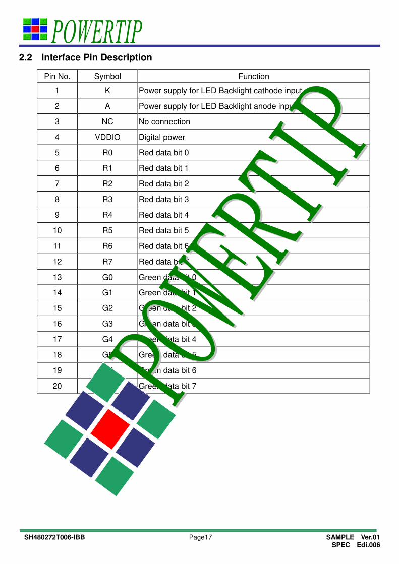
2.2 Interface Pin Description
Pin No. Symbol Function
1 K Power supply for LED Backlight cathode input
2 A Power supply for LED Backlight anode input
3 NC No connection
4 VDDIO Digital power
5 R0 Red data bit 0
6 R1 Red data bit 1
7 R2 Red data bit 2
8 R3 Red data bit 3
9 R4 Red data bit 4
10 R5 Red data bit 5
11 R6 Red data bit 6
12 R7 Red data bit 7
13 G0 Green data bit 0
14 G1 Green data bit 1
15 G2 Green data bit 2
16 G3 Green data bit 3
17 G4 Green data bit 4
18 G5 Green data bit 5
19 G6 Green data bit 6
20 G7 Green data bit 7
SH480272T006-IBB Page18 SAMPLE Ver.01 SPEC Edi.006
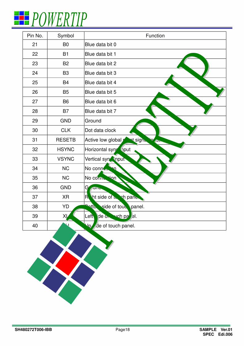
Pin No. Symbol Function
21 B0 Blue data bit 0
22 B1 Blue data bit 1
23 B2 Blue data bit 2
24 B3 Blue data bit 3
25 B4 Blue data bit 4
26 B5 Blue data bit 5
27 B6 Blue data bit 6
28 B7 Blue data bit 7
29 GND Ground
30 CLK Dot data clock
31 RESETB Active low global reset signal input.
32 HSYNC Horizontal sync input
33 VSYNC Vertical sync input
34 NC No connection
35 NC No connection
36 GND Ground
37 XR Right side of touch panel.
38 YD Bottom side of touch panel.
39 XL Left side of touch panel.
40 YU Up side of touch panel.

SH480272T006-IBB Page19 SAMPLE Ver.01 SPEC Edi.006
2.3 Timing Characteristics
2.3.1 AC Characteristics
VDDIO=3.3V,TA=-20~70℃
2.3.2 AC Timing Diagram
Clock and Data Input Timing Diagram
SH480272T006-IBB Page20 SAMPLE Ver.01 SPEC Edi.006
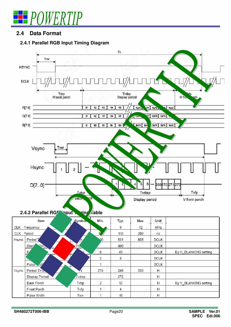
2.4 Data Format
2.4.1 Parallel RGB Input Timing Diagram
2.4.2 Parallel RGB Input Timing Table

SH480272T006-IBB Page21 SAMPLE Ver.01 SPEC Edi.006
2.5 Power On/Off Sequence
2.5.1 Power On Sequence
2.5.2 Power Off Sequence
SH480272T006-IBB Page22 SAMPLE Ver.01 SPEC Edi.006
3. QUALITY ASSURANCE SYSTEM
3.1 Quality Assurance Flow Chart
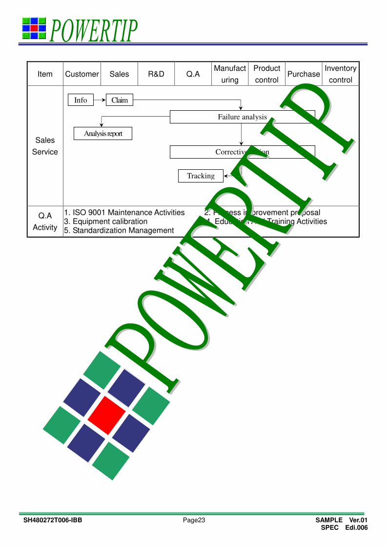
Item Customer Sales R&D Q.A Manufactu
ring
Product
control Purchase
Inventory
control
Marketing
&
Design
Sample
Approval
Pilot
Run
&
Mass
Product
Ship
Out
OK
Request
Info Survey
Inquiry Project evaluation
Project Validation
Quote OK
NG
Contract
Design check
Sample test
Verification
Sample approval
NG
NG
Pilot run & Reliability test
Verification
Specification preparation
OK
Mass production
Inspection NG OK
Shipment
NG
Ship out
OK
SH480272T006-IBB Page23 SAMPLE Ver.01 SPEC Edi.006
Item Customer Sales R&D Q.A Manufact
uring
Product
control Purchase
Inventory
control
Sales
Service
Q.A
Activity
1. ISO 9001 Maintenance Activities 2. Process improvement proposal 3. Equipment calibration 4. Education And Training Activities 5. Standardization Management
Info Claim
Failure analysis
Corrective action
Tracking
Analysis report
SH480272T006-IBB Page24 SAMPLE Ver.01 SPEC Edi.006
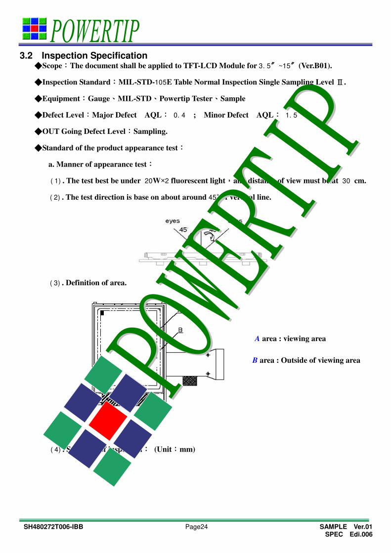
3.2 Inspection Specification ◆Scope:The document shall be applied to TFT-LCD Module for 3. 5〞~15〞(Ver.B01).
◆Inspection Standard:MIL-STD-105E Table Normal Inspection Single Sampling Level Ⅱ.
◆Equipment:Gauge、MIL-STD、Powertip Tester、Sample
◆Defect Level:Major Defect AQL: 0. 4 ; Minor Defect AQL: 1. 5
◆OUT Going Defect Level:Sampling.
◆Standard of the product appearance test:
a. Manner of appearance test:
( 1) . The test best be under 20W×2 fluorescent light,and distance of view must be at 30 cm.
( 2) . The test direction is base on about around 45˚ of vertical line.
( 3) . Definition of area.
( 4) . Standard of inspection: (Unit:mm)
A area : viewing area
B area : Outside of viewing area

SH480272T006-IBB Page25 SAMPLE Ver.01 SPEC Edi.006
◆Specification For TFT-LCD Module 3. 5〞~15〞: (Ver.B01)
NO Item Criterion Level
01 Product condition
1. 1The part number is inconsistent with work order of
production. Major
1. 2 Mixed product types. Major
1. 3 Assembled in inverse direction. Major
02 Quantity 2. 1The quantity is inconsistent with work order of production. Major
03 Outline dimension 3. 1 Product dimension and structure must conform to structure
diagram. Major
04 Electrical Testing
4. 1 Missing line character and icon. Major
4. 2 No function or no display. Major
4. 3 Display malfunction. Major
4. 4 LCD viewing angle defect. Major
4. 5 Current consumption exceeds product specifications. Major
4. 6 Mura can not be seen through 5% ND filter.
(Mura : Under the normal examination angle of view,the
picture has the non-uniform phenomenon.)
Minor
05
Dot defect
(Bright dot、
Dark dot)
On -display
Item Acceptance (Q’ty)
Dot
Defect
Bright Dot ≦ 4
Dark Dot ≦ 5
Joint Dot ≦ 3
Total ≦ 7
5. 1 Inspection pattern:full white , full black , Red , Green and
blue screens.
5. 2 It is defined as dot defect if defect area >1/ 2 dot.
5. 3 The distance between two dot defect ≧5 mm.
5. 4 Br i ght dot t hat can not be seen t hr ough 5% ND f i l t er .
Minor
SH480272T006-IBB Page26 SAMPLE Ver.01 SPEC Edi.006
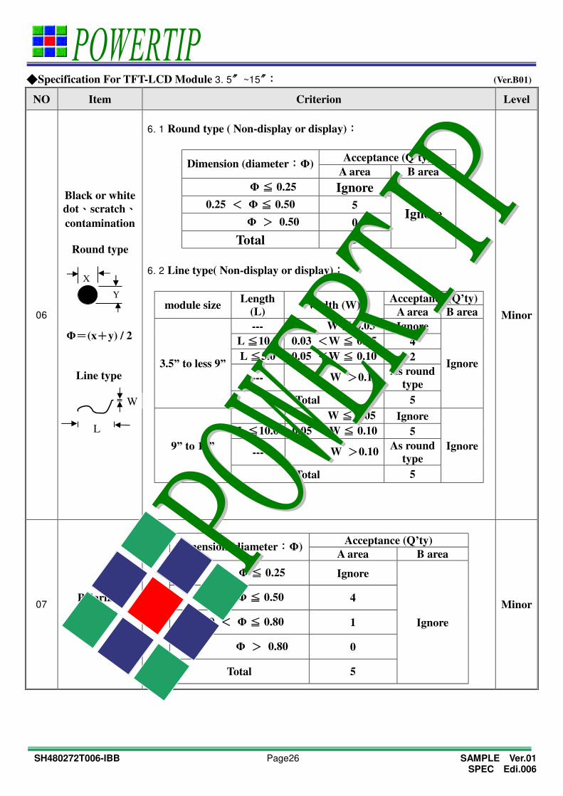
◆Specification For TFT-LCD Module 3. 5〞~15〞: (Ver.B01)
NO Item Criterion Level
06
Black or white
dot、scratch、
contamination
Round type
6. 1 Round type ( Non-display or display):
Dimension (diameter:Φ) Acceptance (Q’ty)
A area B area
Φ ≦ 0.25 Ignore
Ignore 0.25 < Φ ≦ 0.50 5
Φ > 0.50 0
Total 5
6. 2 Line type( Non-display or display):
module size Length
(L) Width (W)
Acceptance (Q’ty)
A area B area
3.5” to less 9”
--- W ≦ 0.03 Ignore
Ignore
L ≦10.0 0.03 <W ≦ 0.05 4
L ≦5.0 0.05 <W ≦ 0.10 2
--- W >0.10 As round
type
Total 5
9” to 15”
--- W ≦ 0.05 Ignore
Ignore
L ≦10.0 0.05 <W ≦ 0.10 5
--- W >0.10 As round
type
Total 5
Minor
07 Polarizer
Bubble
Dimension (diameter:Φ) Acceptance (Q’ty)
A area B area
Φ ≦ 0.25 Ignore
Ignore
0.25 < Φ ≦ 0.50 4
0.50 < Φ ≦ 0.80 1
Φ > 0.80 0
Total 5
Minor
X
Y
Φ=(x+y) / 2
W
L
Line type
SH480272T006-IBB Page27 SAMPLE Ver.01 SPEC Edi.006
◆Specification For TFT-LCD Module 3. 5〞~15〞: (Ver.B01)
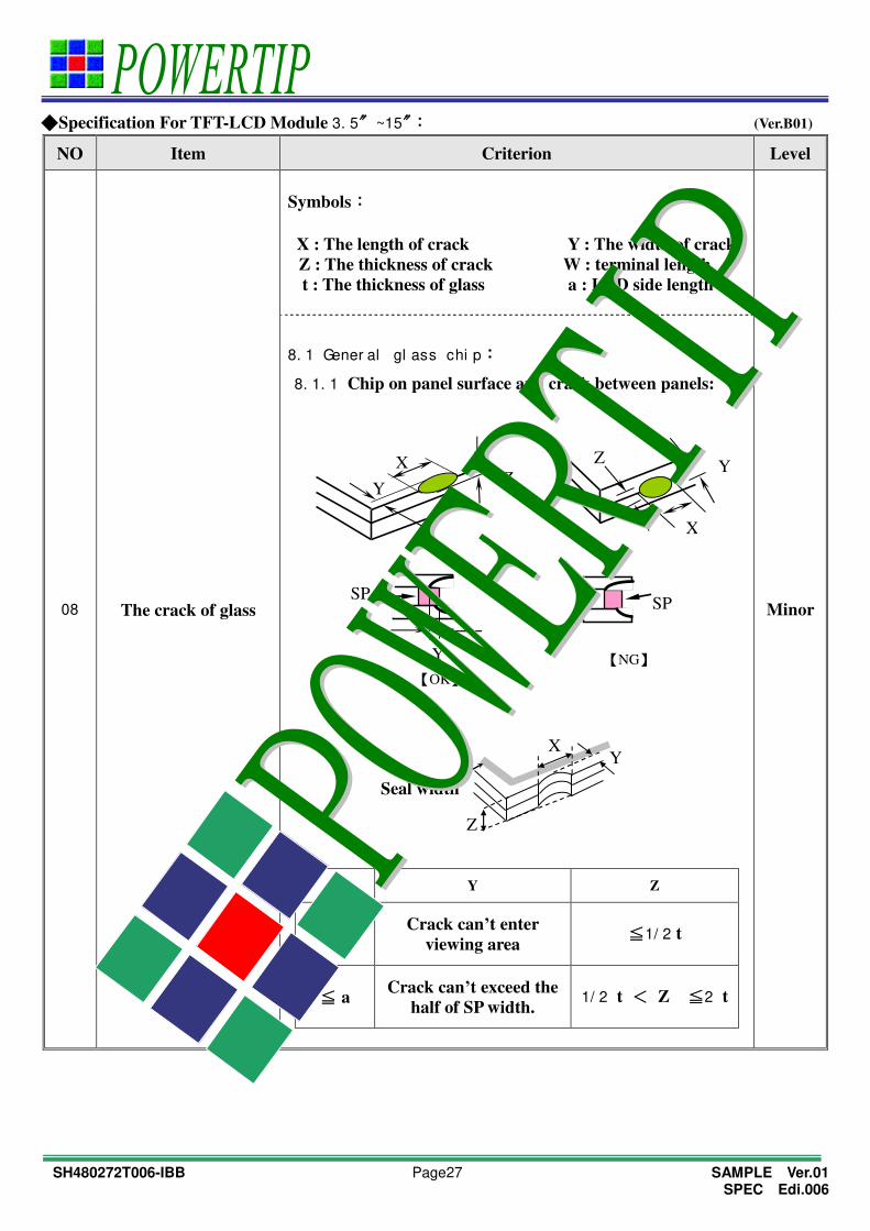
NO Item Criterion Level
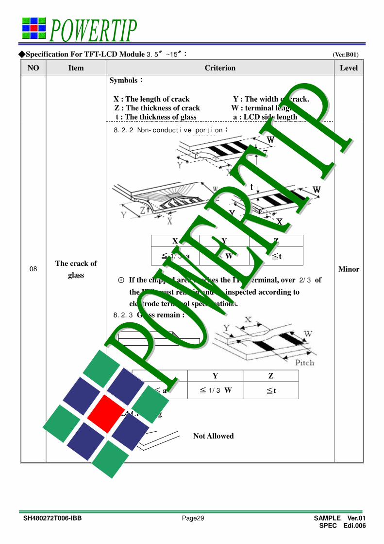
08 The crack of glass
Symbols:
X : The length of crack Y : The width of crack.
Z : The thickness of crack W : terminal length
t : The thickness of glass a : LCD side length
Minor
8. 1 Gener al gl ass chi p:
8. 1. 1 Chip on panel surface and crack between panels:
X
Y
SP
【OK】
SP
【NG】
X Y Z
≦ a Crack can’t enter
viewing area ≦1/ 2 t
≦ a Crack can’t exceed the
half of SP width. 1/ 2 t < Z ≦2 t
X
Y Z
Y Z
X Y
Z
Seal width

SH480272T006-IBB Page28 SAMPLE Ver.01 SPEC Edi.006
◆Specification For TFT-LCD Module 3. 5〞~15〞: (Ver.B01)
NO Item Criterion Level
08 The crack of glass
Symbols:
X : The length of crack Y : The width of crack.
Z : The thickness of crack W : terminal length
t : The thickness of glass a : LCD side length
Minor
8. 1. 2 Cor ner cr ack:
8. 2 Pr ot r usi on over t er mi nal:
8. 2. 1 Chi p on el ect r ode pad:
Z
X Y
X Y Z
Front ≦ a ≦ 1/ 2 W ≦ t
Back ≦ a ≦ W ≦ 1/ 2 t
X
Y
Z
X Y Z
≦1/ 5 a Crack can’t enter
viewing area Z ≦ 1/ 2 t
≦1/ 5 a Crack can’t exceed the
half of SP width. 1/ 2 t < Z ≦ 2 t
W
SH480272T006-IBB Page29 SAMPLE Ver.01 SPEC Edi.006
◆Specification For TFT-LCD Module 3. 5〞~15〞: (Ver.B01)
NO Item Criterion Level
08 The crack of
glass
Symbols:
X : The length of crack Y : The width of crack.
Z : The thickness of crack W : terminal length
t : The thickness of glass a : LCD side length
Minor
8. 2. 2 Non- conduct i ve por t i on:
⊙ If the chipped area touches the ITO terminal, over 2/ 3 of
the ITO must remain and be inspected according to
electrode terminal specifications.
8. 2. 3 Glass remain :
8.2.4 Cracking
X Y Z
≦ a ≦ 1/ 3 W ≦t
X Y Z
≦ 1/ 3 a ≦ W ≦t
Not Allowed

SH480272T006-IBB Page30 SAMPLE Ver.01 SPEC Edi.006
◆Specification For TFT-LCD Module 3. 5〞~15〞: (Ver.B01)
NO Item Criterion Level
09 Backlight
elements
9. 1 Backlight can’t work normally. Major
9. 2 Backlight doesn’t light or color is wrong. Major
9. 3 Illumination source flickers when lit. Major
10 General
appearance
10. 1 Pin type、quantity、dimension must match type in structure
diagram. Major
10. 2 No short circuits in components on PCB or FPC . Major
10. 3 Parts on PCB or FPC must be the same as on the
production characteristic chart .There should be no wrong
parts , missing parts or excess parts.
Major
10. 4 Product packaging must the same as specified on packaging
specification sheet. Minor
10. 5 The folding and peeled off in polarizer are not acceptable. Minor
10. 6 The PCB or FPC between B/L assembled distance(PCB or
FPC ) is ≦1. 5 mm. Minor

SH480272T006-IBB Page31 SAMPLE Ver.01 SPEC Edi.006
4. RELIABILITY TEST
4.1 Reliability Test Condition (Ver.B01)
NO. TEST ITEM TEST CONDITION
1 High Temperature
Storage Test
Keep in +80 ±2℃ 96 hrs
Surrounding temperature, then storage at normal condition 4hrs.
2 Low Temperature
Storage Test
Keep in - 30 ±2℃ 96 hrs
Surrounding temperature, then storage at normal condition 4hrs.
3
High Temperature /
High Humidity
Storage Test
Keep in +60 ℃ / 90% R.H duration for 96 hrs
Surrounding temperature, then storage at normal condition 4hrs.
(Excluding the polarizer)
4 Temperature Cycling
Storage Test
- 30℃ → +25℃ → +80℃ → +25℃
(30mins) (5mins) (30mins) (5mins)
10 Cycle
Surrounding temperature, then storage at normal condition 4hrs.
5 ESD Test
Air Discharge:
Apply 2 KV with 5 times
Discharge for each polarity +/-
Contact Discharge:
Apply 250 V with 5 times
discharge for each polarity +/-
1. Temperature ambiance : 15℃~35℃
2. Humidity relative : 30%~60%
3. Energy Storage Capacitance(Cs+Cd) : 150pF±10%
4. Discharge Resistance(Rd) : 330Ω±10%
5. Discharge, mode of operation :
Single Discharge (time between successive discharges at least 1 sec)
(Tolerance if the output voltage indication : ±5%)
6 Vibration Test
(Packaged)
1. Sine wave 10~55 Hz frequency (1 min/sweep)
2. The amplitude of vibration :1. 5 mm
3. Each direction (X、Y、Z) duration for 2 Hrs
7 Drop Test
(Packaged)
Drop Direction :※1 corner / 3 edges / 6 sides each 1time
Packing Weight (Kg) Drop Height (cm)
0 ~ 45. 4 122
45. 4 ~ 90. 8 76
90. 8 ~ 454 61
Over 454 46
SH480272T006-IBB Page32 SAMPLE Ver.01 SPEC Edi.006
5. PRECAUTION RELATING PRODUCT HANDLING 5.1 SAFETY
5.1.1 If the LCD panel breaks , be careful not to get the liquid crystal to touch your skin.
5.1.2 If the liquid crystal touches your skin or clothes , please wash it off immediately by
using soap and water.
5.2 HANDLING
5.2.1 Avoid any strong mechanical shock which can break the glass.
5.2.2 Avoid static electricity which can damage the CMOS LSI—When working with the
module , be sure to ground your body and any electrical equipment you may be using.
5.2.3 Do not remove the panel or frame from the module.
5.2.4 The polarizing plate of the display is very fragile. So , please handle it very
carefully ,do not touch , push or rub the exposed polarizing with anything harder
than an HB pencil lead (glass , tweezers , etc.)
5.2.5 Do not wipe the polarizing plate with a dry cloth , as it may easily scratch the
surface of plate.
5.2.6 Do not touch the display area with bare hands , this will stain the display area.
5.2.7 Do not use ketonics solvent & aromatic solvent. Use with a soft cloth soaked with
a cleaning naphtha solvent.
5.2.8 To control temperature and time of soldering is 320±10℃and 3-5 sec.
5.2.9 To avoid liquid (include organic solvent) stained on LCM .
5.3 STORAGE 5.3.1 Store the panel or module in a dark place where the temperature is 25℃ ±5℃
and the humidity is below 65% RH.
5.3.2 Do not place the module near organics solvents or corrosive gases.
5.3.3 Do not crush , shake , or jolt the module.
5.4 TERMS OF WARRANTY
5.4.1 Applicable warrant period
The period is within thirteen months since the date of shipping out under normal
using and storage conditions.
5.4.2 Unaccepted responsibility
This product has been manufactured to your company’s specification as a part for
use in your company’s general electronic products. It is guaranteed to perform
according to delivery specifications. For any other use apart from general
electronic equipment , we cannot take responsibility if the product is used in
nuclear power control equipment , aerospace equipment , fire and security
systems or any other applications in which there is a direct risk to human life
and where extremely high levels of reliability are required.