pqmii power quality meter communications guide...pqmii power quality meter – instruction manual...
TRANSCRIPT

GE Consumer & IndustrialMultilin
PQMII Power Quality MeterCommunications Guide
Software Revision: 2.2x
Manual P/N: 1601-9090-A1Manual Order Code: GEK-113532
Copyright © 2009 GE Multilin
GE Multilin
215 Anderson Avenue, Markham, Ontario
Canada L6E 1B3
Tel: (905) 294-6222 Fax: (905) 201-2098
Internet: http://www.GEmultilin.com
GE Multilin's Quality Management System is registered to ISO9001:2000
QMI # 005094UL # A3775*1601-9090-A1*
© 2009 GE Multilin Incorporated. All rights reserved.
GE Multilin PQMII Power Quality Meter instruction manual for revision 2.2x.
PQMII Power Quality Meter, is a registered trademark of GE Multilin Inc.
The contents of this manual are the property of GE Multilin Inc. This documentation is furnished on license and may not be reproduced in whole or in part without the permission of GE Multilin. The content of this manual is for informational use only and is subject to change without notice.
Part numbers contained in this manual are subject to change without notice, and should therefore be verified by GE Multilin before ordering.
Part number: 1601-9090-A1 (April 2009)
TABLE OF CONTENTS
PQMII POWER QUALITY METER – INSTRUCTION MANUAL TOC–1
Table of Contents
COMMUNICATIONS GUIDE
MODBUS OVERVIEW ......................................................................................................1MODBUS PROTOCOL .........................................................................................................1ELECTRICAL INTERFACE .....................................................................................................1DATA FRAME FORMAT AND DATA RATE ........................................................................2DATA PACKET FORMAT .....................................................................................................2ERROR CHECKING .............................................................................................................3CRC-16 ALGORITHM .......................................................................................................3TIMING ................................................................................................................................4READING LONG INTEGERS FROM THE MEMORY MAP ..................................................4
MODBUS FUNCTIONS ....................................................................................................6SUPPORTED MODBUS FUNCTIONS .................................................................................6READ SETPOINTS/ACTUAL VALUES (FUNCTION CODES 03/04H) .............................6EXECUTE OPERATION (FUNCTION CODE 05H) ..............................................................7BROADCAST COMMAND (FUNCTION CODE 05H) .........................................................7STORE SINGLE SETPOINT (FUNCTION CODE 06H) .......................................................8READ DEVICE STATUS (FUNCTION CODE 07H) ............................................................8LOOPBACK TEST (FUNCTION CODE 08H) ......................................................................9STORE MULTIPLE SETPOINTS (FUNCTION CODE 10H) ..............................................10PERFORMING COMMANDS (FUNCTION CODE 10H) ..................................................10BROADCAST COMMAND (FUNCTION CODE 10H) ......................................................11ERROR RESPONSES ........................................................................................................12
MODBUS MEMORY MAP ............................................................................................ 13MEMORY MAP INFORMATION .......................................................................................13USER-DEFINABLE MEMORY MAP .................................................................................13PQMII MEMORY MAP ...................................................................................................14MEMORY MAP DATA FORMATS ....................................................................................57ANALOG OUTPUT PARAMETER RANGE ........................................................................74
DNP 3.0 COMMUNICATIONS .................................................................................... 77DNP 3.0 DEVICE PROFILE DOCUMENT ......................................................................77IMPLEMENTATION TABLE ...............................................................................................78DEFAULT VARIATIONS ....................................................................................................80INTERNAL INDICATION BITS ...........................................................................................80
DNP POINT LISTS ........................................................................................................... 81BINARY INPUT / BINARY INPUT CHANGE ....................................................................81BINARY OUTPUT / CONTROL RELAY OUTPUT ............................................................84ANALOG INPUT/OUTPUT CHANGE ...............................................................................86COUNTERS .......................................................................................................................92

TOC–2 PQMII POWER QUALITY METER – INSTRUCTION MANUAL
TABLE OF CONTENTS
PQMII POWER QUALITY METER – INSTRUCTION MANUAL COMM–1
PQMII Power Quality Meter
Communications Guide
Digital EnergyMultilin
Communications Guide
1 Modbus Overview
1.1 Modbus ProtocolThe GE Multilin PQMII implements a subset of the AEG Modicon Modbus RTU serial communication standard. Many popular programmable controllers support this protocol directly with a suitable interface card allowing direct connection of the PQMII. Although the Modbus protocol is hardware independent, the PQMII interface uses 2-wire RS485 and 9-pin RS232 interfaces. Modbus is a single-master multiple-slave protocol suitable for a multi-drop configuration provided by RS485 hardware. In this configuration, up to 32 slaves can be daisy-chained together on a single communication channel.
The PQMII is always a Modbus slave; it cannot be programmed as a Modbus master. Computers or PLCs are commonly programmed as masters. The Modbus protocol exists in two versions: Remote Terminal Unit (RTU, binary) and ASCII. Only the RTU version is supported by the PQMII. Monitoring, programming and control functions are possible using read and write register commands.
1.2 Electrical InterfaceThe electrical interface is 2-wire RS485 and 9-pin RS232. In a 2-wire RS485 link, data flow is bi-directional and half duplex. That is, data is never transmitted and received at the same time. RS485 lines should be connected in a daisy-chain configuration (avoid star connections) with a terminating network installed at each end of the link, i.e. at the master end and the slave farthest from the master. The terminating network should consist of a 120 Ω resistor in series with a 1 nF ceramic capacitor when used with Belden 9841 RS485 wire. The value of the terminating resistors should be equal to the characteristic impedance of the line. This is approximately 120 Ω for standard #22 AWG twisted-pair wire. Shielded wire should always be used to minimize noise. Polarity is important in RS485

COMM–2 PQMII POWER QUALITY METER – INSTRUCTION MANUAL
CHAPTER COMM: COMMUNICATIONS GUIDE
communications: each '+' terminal of every device must be connected together for the system to operate. See PQMII Intstruction Manual section 2.2.11: RS485 Serial Ports for details on serial port wiring.
1.3 Data Frame Format and Data RateOne data frame of an asynchronous transmission to or from a PQMII consists of 1 start bit, 8 data bits, and 1 stop bit, resulting in a 10-bit data frame. This is important for high-speed modem transmission, since 11-bit data frames are not supported by Hayes modems at bit rates greater than 300 bps. The Modbus protocol can be implemented at any standard communication speed. The PQMII supports operation at 1200, 2400, 4800, 9600, and 19200 baud.
1.4 Data Packet FormatA complete request/response sequence consists of the following bytes (transmitted as separate data frames):
Master Request Transmission:
SLAVE ADDRESS: 1 byteFUNCTION CODE: 1 byteDATA: variable number of bytes depending on the Function CodeCRC: 2 bytes
Slave Response Transmission:
SLAVE ADDRESS: 1 byteFUNCTION CODE: 1 byteDATA: variable number of bytes depending on FUNCTION CODECRC: 2 bytes
The Slave Address is the first byte of every transmission. It represents the user-assigned address of the slave device assigned to receive the message sent by the master. Each slave device must be assigned a unique address so only it responds to a transmission that starts with its address. In a master request transmission, the Slave Address represents the address to which the request is being sent. In a slave response transmission the Slave Address represents the address sending the response.
Note A master transmission with a Slave Address of 0 indicates a broadcast command. Broadcast commands can be used only to store setpoints or perform commands.
The Function Code is the second byte of every transmission. Modbus defines function codes of 1 to 127. The PQMII implements some of these functions. See 2.1 Supported Modbus Functions for details of the supported function codes. In a master request transmission the Function Code tells the slave what action to perform. In a slave response transmission if the Function Code sent from the slave is the same as the Function Code sent from the master then the slave performed the function as requested. If the high order bit of the Function Code sent from the slave is a 1 (i.e. if the Function Code is > 127) then the slave did not perform the function as requested and is sending an error or exception response.
CHAPTER COMM: COMMUNICATIONS GUIDE
PQMII POWER QUALITY METER – INSTRUCTION MANUAL COMM–3
The Data is a variable number of bytes depending on the Function Code. This may be Actual Values, Setpoints, or addresses sent by the master to the slave or by the slave to the master. See 2.1 Supported Modbus Functions for a description of the supported functions and the data required for each.
The CRC is a a two byte error checking code. See the following section for details.
1.5 Error CheckingThe RTU version of Modbus includes a 2-byte CRC-16 (16-bit cyclic redundancy check) with every transmission. The CRC-16 algorithm essentially treats the entire data stream (data bits only; start, stop and parity are ignored) as one continuous binary number. This number is first shifted left 16 bits and then divided by a characteristic polynomial (11000000000000101B). The 16-bit remainder is appended to the end of the transmission, MSByte first. The resulting message including CRC, when divided by the same polynomial at the receiver, results in a zero remainder if no transmission errors have occurred.
If a PQMII Modbus slave device receives a transmission in which an error is indicated by the CRC-16 calculation, the slave device will not respond to the transmission. A CRC-16 error indicates that one or more bytes of the transmission were received incorrectly and thus the entire transmission should be ignored in order to avoid the PQMII performing any incorrect operation.
The CRC-16 calculation is an industry standard method used for error detection. An algorithm is included here to assist programmers in situations where no standard CRC-16 calculation routines are available.
1.6 CRC-16 AlgorithmOnce the following algorithm is complete, the working register “A” will contain the CRC value to be transmitted. Note that this algorithm requires the characteristic polynomial to be reverse bit ordered. The MSbit of the characteristic polynomial is dropped since it does not affect the value of the remainder. The following symbols are used in the algorithm:
-->: data transfer;A: 16-bit working register;AL: low order byte of A;AH: high order byte of A;CRC: 16-bit CRC-16 value;i and j: loop counters;(+): logical exclusive-OR operator;Di: i-th data byte (i = 0 to N – 1);G: 16-bit characteristic polynomial = 1010000000000001 with MSbit dropped and bit order reversed;shr(x): shift right (the LSbit of the low order byte of x shifts into a carry flag, a '0' is shifted into the MSbit of the high order byte of x, all other bits shift right one location
The algorithm is shown below:
1. FFFF hex --> A2. 0 --> i3. 0 --> j
COMM–4 PQMII POWER QUALITY METER – INSTRUCTION MANUAL
CHAPTER COMM: COMMUNICATIONS GUIDE
4. Di (+) AL --> AL5. j + 1 --> j6. shr(A)7. is there a carry? No: go to 8; Yes: G (+) A --> A8. is j = 8? No: go to 5; Yes: go to 9.9. i + 1 --> i10. is i = N? No: go to 3; Yes: go to 11.11. A --> CRC
1.7 TimingData packet synchronization is maintained by timing constraints. The receiving device must measure the time between the reception of characters. If three and one half character times elapse without a new character or completion of the packet, then the communication link must be reset (i.e. all slaves start listening for a new transmission from the master). Thus at 9600 baud a delay of greater than 3.5 × 1/9600 × 10 = 3.65 ms will cause the communication link to be reset.
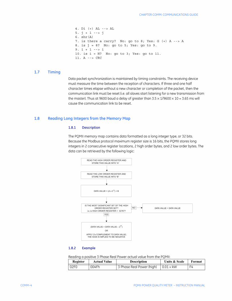
1.8 Reading Long Integers from the Memory Map
1.8.1 Description
The PQMII memory map contains data formatted as a long integer type, or 32 bits. Because the Modbus protocol maximum register size is 16 bits, the PQMII stores long integers in 2 consecutive register locations, 2 high order bytes, and 2 low order bytes. The data can be retrieved by the following logic:
1.8.2 Example
Reading a positive 3 Phase Real Power actual value from the PQMII:Register Actual Value Description Units & Scale Format
02F0 004Fh 3 Phase Real Power (high) 0.01 × kW F4
READ THE HIGH ORDER REGISTER ANDSTORE THIS VALUE INTO “A”
READ THE LOW ORDER REGISTER ANDSTORE THIS VALUE INTO “B”
IS THE MOST SIGNIFICANT BIT OF THE HIGHORDER REGISTER SET?
i.e. is HIGH ORDER REGISTER > 32767?
YES
DATA VALUE = (A x 2 ) + B16
NO
(DATA VALUE = DATA VALUE – 232)
OR
APPLY 2’s COMPLEMENT TO DATA VALUE;THE SIGN IS IMPLIED TO BE NEGATIVE
DATA VALUE = DATA VALUE
CHAPTER COMM: COMMUNICATIONS GUIDE
PQMII POWER QUALITY METER – INSTRUCTION MANUAL COMM–5
Following the method described above, we have:
DATA VALUE = (004F × 216) + 35D1 hexadecimal= 5177344 + 13777 converted to decimal= 5191121 decimal
The most significant bit of the High Order register is not set, therefore the Data Value is as calculated. Applying the Units and Scale parameters to the Data Value, we multiply the Data Value by 0.01 kW. Therefore the resultant value of 3 Phase Real Power as read from the memory map is 51911.21 kW.
Reading a negative 3 Phase Real Power actual value from the PQMII:
Following the method described above:
DATA VALUE = (FF3A × 216) + EA7B hexadecimal= (65338 × 216) + 60027 converted to decimal= 4282051195 decimal
The most significant bit of the High Order register is set, therefore the Data Value is:
DATA VALUE = DATA VALUE – 232 = 4282051195 – 4294967296 = –12916101
Multiply the Data Value by 0.01 kW according to the Units and Scale parameter. The resultant 3 Phase Real Power value read from the memory map is –129161.01 kW.
02F1 35D1h 3 Phase Real Power (low) 0.01 × kW F4
Register Actual Value Description Units & Scale Format02F0 FF3Ah 3 Phase Real Power (high) 0.01 × kW F402F1 EA7Bh 3 Phase Real Power (low) 0.01 × kW F4
Register Actual Value Description Units & Scale Format
COMM–6 PQMII POWER QUALITY METER – INSTRUCTION MANUAL
CHAPTER COMM: COMMUNICATIONS GUIDE
2 Modbus Functions
2.1 Supported Modbus FunctionsThe following functions are supported by the PQMII:
03h: Read Setpoints and Actual Values
04h: Read Setpoints and Actual Values
05h: Execute Operation
06h: Store Single Setpoint
07h: Read Device Status
08h: Loopback Test
10h: Store Multiple Setpoints
2.2 Read Setpoints/Actual Values (Function Codes 03/04h)Modbus implementation: Read Input and Holding RegistersPQMII Implementation: Read Setpoints and Actual Values
For the PQMII Modbus implementation, these commands are used to read any setpoint (‘holding registers’) or actual value (‘input registers’). Holding and input registers are 16-bit (two byte) values with the high-order byte transmitted first. Thus, all setpoints and actual values are sent as two bytes. A maximum of 125 registers can be read in one transmission. Function codes 03 and 04 are configured to read setpoints or actual values interchangeably since some PLCs do not support both of them.
The slave response to function codes 03/04 is the slave address, function code, number of data bytes to follow, the data, and the CRC. Each data item is sent as a 2 byte number with the high order byte first.
Message Format and Example for Modbus Function Code 03/04h:
Request slave 17 to respond with 3 registers starting at address 006B. For this example the register data in these addresses is:
The master/slave packet format is shown below:
Address: 006B 006C 006DData: 022B 0000 0064
Master Transmission Bytes Example DescriptionSlave Address 1 11 message for slave 17Function Code 1 03 read registersData Starting Address 2 00 6B data starting at 006BNumber Of Setpoints 2 00 03 3 registers = 6 bytes totalCRC 2 9D 8D CRC error code
Slave Response Bytes Example DescriptionSlave Address 1 11 message from slave 17
CHAPTER COMM: COMMUNICATIONS GUIDE
PQMII POWER QUALITY METER – INSTRUCTION MANUAL COMM–7
2.3 Execute Operation (Function Code 05h)Modbus Implementation: Force Single CoilPQMII Implementation: Execute Operation
This function code allows the master to request a PQMII to perform specific command operations. The command numbers listed in the Commands area of the memory map correspond to operation codes for function code 05.
The operation commands can also be initiated by writing to the Commands area of the memory map using function code 16. 2.9 Performing Commands (Function Code 10h) for complete details.
Message Format and Example for Modbus Function Code 05h:
Reset PQMII (operation code 1).
2.4 Broadcast Command (Function Code 05h)Modbus Implementation: Force Single CoilPQMII Implementation: Execute Operation
This function code allows the master to request all PQMIIs on a particular communications link to Clear All Demand Data. The PQMII will recognize a packet as being a broadcast command if the Slave Address is transmitted as 0. Below is an example of the Broadcast Command to Clear All Demand Data.
Message Format and Example for Modbus Function Code 05h:
Function Code 1 03 read registersByte Count 1 06 3 registers = 6 bytesData 1 (see definition above) 2 02 2B value in address 006BData 2 (see definition above) 2 00 00 value in address 006CData 3 (see definition above) 2 00 64 value in address 006DCRC 2 C8 B8 CRC error code
Slave Response Bytes Example Description
Master Transmission Bytes Example DescriptionSlave Address 1 11 message for slave 17Function Code 1 05 execute operationOperation Code 2 00 01 Reset command (operation code 1)Code Value 2 FF 00 perform functionCRC 2 DF 6A CRC error code
Slave Response Bytes Example DescriptionSlave Address 1 11 message from slave 17Function Code 1 05 execute operationOperation Code 2 00 01 operation code 1Code Value 2 FF 00 perform functionCRC 2 DF 6A CRC error code
COMM–8 PQMII POWER QUALITY METER – INSTRUCTION MANUAL
CHAPTER COMM: COMMUNICATIONS GUIDE
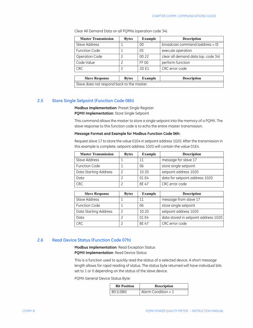
Clear All Demand Data on all PQMIIs (operation code 34).
2.5 Store Single Setpoint (Function Code 06h)Modbus Implementation: Preset Single RegisterPQMII Implementation: Store Single Setpoint
This command allows the master to store a single setpoint into the memory of a PQMII. The slave response to this function code is to echo the entire master transmission.
Message Format and Example for Modbus Function Code 06h:
Request slave 17 to store the value 01E4 in setpoint address 1020. After the transmission in this example is complete, setpoint address 1020 will contain the value 01E4.
2.6 Read Device Status (Function Code 07h)Modbus Implementation: Read Exception StatusPQMII Implementation: Read Device Status
This is a function used to quickly read the status of a selected device. A short message length allows for rapid reading of status. The status byte returned will have individual bits set to 1 or 0 depending on the status of the slave device.
PQMII General Device Status Byte:
Master Transmission Bytes Example DescriptionSlave Address 1 00 broadcast command (address = 0)Function Code 1 05 execute operationOperation Code 2 00 22 clear all demand data (op. code 34)Code Value 2 FF 00 perform functionCRC 2 2D E1 CRC error code
Slave Response Bytes Example DescriptionSlave does not respond back to the master.
Master Transmission Bytes Example DescriptionSlave Address 1 11 message for slave 17Function Code 1 06 store single setpointData Starting Address 2 10 20 setpoint address 1020Data 2 01 E4 data for setpoint address 1020CRC 2 8E 47 CRC error code
Slave Response Bytes Example DescriptionSlave Address 1 11 message from slave 17Function Code 1 06 store single setpointData Starting Address 2 10 20 setpoint address 1020Data 2 01 E4 data stored in setpoint address 1020CRC 2 8E 47 CRC error code
Bit Position DescriptionB0 (LSBit) Alarm Condition = 1
CHAPTER COMM: COMMUNICATIONS GUIDE
PQMII POWER QUALITY METER – INSTRUCTION MANUAL COMM–9
Message Format and Example for Modbus Function Code 07h:
Request status from slave 17.
2.7 Loopback Test (Function Code 08h)Modbus Implementation: Loopback TestPQMII Implementation: Loopback Test
This function is used to test the integrity of the communication link. The PQMII will echo the request.
Message Format and Example for Modbus Function 08h:
Loopback test from slave 17.
B1 Self test failure = 1B2 Alarm relay energized = 1B3 Aux 1 relay energized = 1B4 Aux 2 relay energized = 1B5 Aux 3 relay energized = 1B6 Not usedB7 (MSBit) Not used
Master Transmission Bytes Example DescriptionSlave Address 1 11 message for slave 17Function Code 1 07 read device statusCRC 2 4C 22 CRC error code
Slave Response Bytes Example DescriptionSlave Address 1 11 message from slave 17Function Code 1 07 read device statusDevice Status (see above) 2 2C status = 00101100 (in binary)CRC 2 22 28 CRC error code
Bit Position Description
Master Transmission Bytes Example DescriptionSlave Address 1 11 message for slave 17Function Code 1 08 loopback testDiagnostic code 2 00 00 must be 00 00Data 2 00 00 must be 00 00CRC 2 E0 0B CRC error code
Slave Response Bytes Example DescriptionSlave Address 1 11 message from slave 17Function Code 1 08 loopback testDiagnostic Code 2 00 00 must be 00 00Data 2 00 00 must be 00 00CRC 2 E0 0B CRC error code
COMM–10 PQMII POWER QUALITY METER – INSTRUCTION MANUAL
CHAPTER COMM: COMMUNICATIONS GUIDE
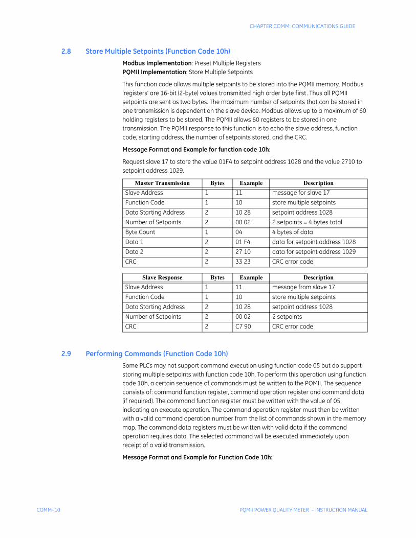
2.8 Store Multiple Setpoints (Function Code 10h)Modbus Implementation: Preset Multiple RegistersPQMII Implementation: Store Multiple Setpoints
This function code allows multiple setpoints to be stored into the PQMII memory. Modbus ‘registers’ are 16-bit (2-byte) values transmitted high order byte first. Thus all PQMII setpoints are sent as two bytes. The maximum number of setpoints that can be stored in one transmission is dependent on the slave device. Modbus allows up to a maximum of 60 holding registers to be stored. The PQMII allows 60 registers to be stored in one transmission. The PQMII response to this function is to echo the slave address, function code, starting address, the number of setpoints stored, and the CRC.
Message Format and Example for function code 10h:
Request slave 17 to store the value 01F4 to setpoint address 1028 and the value 2710 to setpoint address 1029.
2.9 Performing Commands (Function Code 10h)Some PLCs may not support command execution using function code 05 but do support storing multiple setpoints with function code 10h. To perform this operation using function code 10h, a certain sequence of commands must be written to the PQMII. The sequence consists of: command function register, command operation register and command data (if required). The command function register must be written with the value of 05, indicating an execute operation. The command operation register must then be written with a valid command operation number from the list of commands shown in the memory map. The command data registers must be written with valid data if the command operation requires data. The selected command will be executed immediately upon receipt of a valid transmission.
Message Format and Example for Function Code 10h:
Master Transmission Bytes Example DescriptionSlave Address 1 11 message for slave 17Function Code 1 10 store multiple setpointsData Starting Address 2 10 28 setpoint address 1028Number of Setpoints 2 00 02 2 setpoints = 4 bytes totalByte Count 1 04 4 bytes of dataData 1 2 01 F4 data for setpoint address 1028Data 2 2 27 10 data for setpoint address 1029CRC 2 33 23 CRC error code
Slave Response Bytes Example DescriptionSlave Address 1 11 message from slave 17Function Code 1 10 store multiple setpointsData Starting Address 2 10 28 setpoint address 1028Number of Setpoints 2 00 02 2 setpointsCRC 2 C7 90 CRC error code
CHAPTER COMM: COMMUNICATIONS GUIDE
PQMII POWER QUALITY METER – INSTRUCTION MANUAL COMM–11
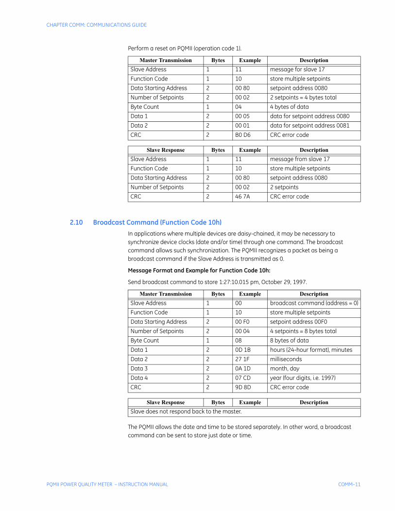
Perform a reset on PQMII (operation code 1).
2.10 Broadcast Command (Function Code 10h)In applications where multiple devices are daisy-chained, it may be necessary to synchronize device clocks (date and/or time) through one command. The broadcast command allows such synchronization. The PQMII recognizes a packet as being a broadcast command if the Slave Address is transmitted as 0.
Message Format and Example for Function Code 10h:
Send broadcast command to store 1:27:10.015 pm, October 29, 1997.
The PQMII allows the date and time to be stored separately. In other word, a broadcast command can be sent to store just date or time.
Master Transmission Bytes Example DescriptionSlave Address 1 11 message for slave 17Function Code 1 10 store multiple setpointsData Starting Address 2 00 80 setpoint address 0080Number of Setpoints 2 00 02 2 setpoints = 4 bytes totalByte Count 1 04 4 bytes of dataData 1 2 00 05 data for setpoint address 0080Data 2 2 00 01 data for setpoint address 0081CRC 2 B0 D6 CRC error code
Slave Response Bytes Example DescriptionSlave Address 1 11 message from slave 17Function Code 1 10 store multiple setpointsData Starting Address 2 00 80 setpoint address 0080Number of Setpoints 2 00 02 2 setpointsCRC 2 46 7A CRC error code
Master Transmission Bytes Example DescriptionSlave Address 1 00 broadcast command (address = 0)Function Code 1 10 store multiple setpointsData Starting Address 2 00 F0 setpoint address 00F0Number of Setpoints 2 00 04 4 setpoints = 8 bytes totalByte Count 1 08 8 bytes of dataData 1 2 0D 1B hours (24-hour format), minutesData 2 2 27 1F millisecondsData 3 2 0A 1D month, dayData 4 2 07 CD year (four digits, i.e. 1997)CRC 2 9D 8D CRC error code
Slave Response Bytes Example DescriptionSlave does not respond back to the master.
COMM–12 PQMII POWER QUALITY METER – INSTRUCTION MANUAL
CHAPTER COMM: COMMUNICATIONS GUIDE
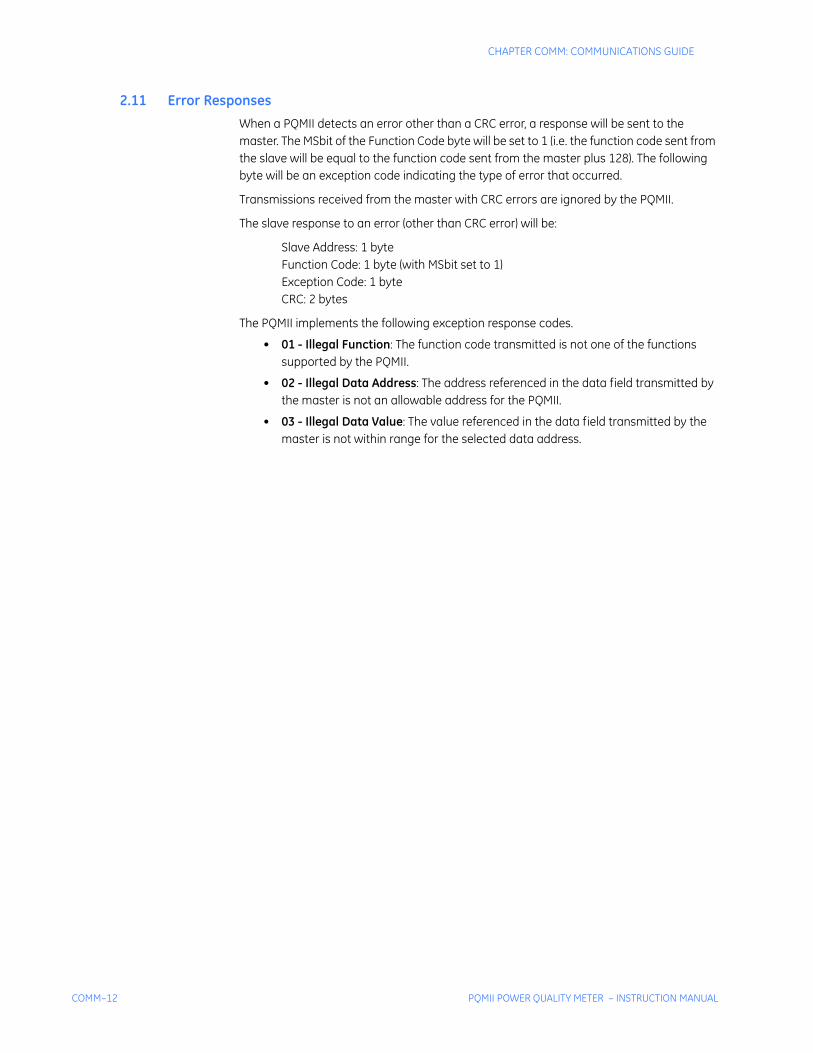
2.11 Error ResponsesWhen a PQMII detects an error other than a CRC error, a response will be sent to the master. The MSbit of the Function Code byte will be set to 1 (i.e. the function code sent from the slave will be equal to the function code sent from the master plus 128). The following byte will be an exception code indicating the type of error that occurred.
Transmissions received from the master with CRC errors are ignored by the PQMII.
The slave response to an error (other than CRC error) will be:
Slave Address: 1 byteFunction Code: 1 byte (with MSbit set to 1)Exception Code: 1 byteCRC: 2 bytes
The PQMII implements the following exception response codes.
• 01 - Illegal Function: The function code transmitted is not one of the functions supported by the PQMII.
• 02 - Illegal Data Address: The address referenced in the data field transmitted by the master is not an allowable address for the PQMII.
• 03 - Illegal Data Value: The value referenced in the data field transmitted by the master is not within range for the selected data address.
CHAPTER COMM: COMMUNICATIONS GUIDE
PQMII POWER QUALITY METER – INSTRUCTION MANUAL COMM–13
3 Modbus Memory Map
3.1 Memory Map InformationThe data stored in the PQMII are grouped by setpoints and actual values. Setpoints can be read and written by a master computer; actual values are read-only. All setpoints and actual values are stored as two-byte values; that is, each register address is the address of a two-byte value. In the Modbus memory map, addresses are shown in hexadecimal notation; data values (setpoint ranges, increments, factory values) are in decimal notation.
3.2 User-definable Memory MapThe PQMII contains a user-definable area in the memory map. This area allows remapping of the addresses of all actual values and setpoints registers. The user-definable area has two sections:
• A Register Index area (memory map addresses 0180h to 01F7h) that contains 120 actual values or setpoints register addresses.
• A Register area (memory map addresses 0100h to 017Fh) that contains the data at the addresses in the Register Index.
Register data that is separated in the rest of the memory map may be remapped to adjacent register addresses in the user-definable registers area. This is accomplished by writing to register addresses in the user-definable register index area. This allows for improved throughput of data and can eliminate the need for multiple read command sequences.
For example, if the values of Phase A Current (register address 0240h) and Phase A Power Factor (register address 02FDh) are required to be read from a PQMII, their addresses may be remapped as follows:
1. Write 0240h to address 0180h (User-Definable Register Index 0000) using Modbus function code 06h or 10h.
2. Write 02FDh to address 0181h (User-Definable Register Index 0001) using Modbus function code 06h or 10h.
A read (function code 03h or 04h) of registers 0100h (User-Definable Register 0000) and 0101h (User-Definable Register 0001) will return the Phase A Current and Phase A Power Factor.
COMM–14 PQMII POWER QUALITY METER – INSTRUCTION MANUAL
CHAPTER COMM: COMMUNICATIONS GUIDE
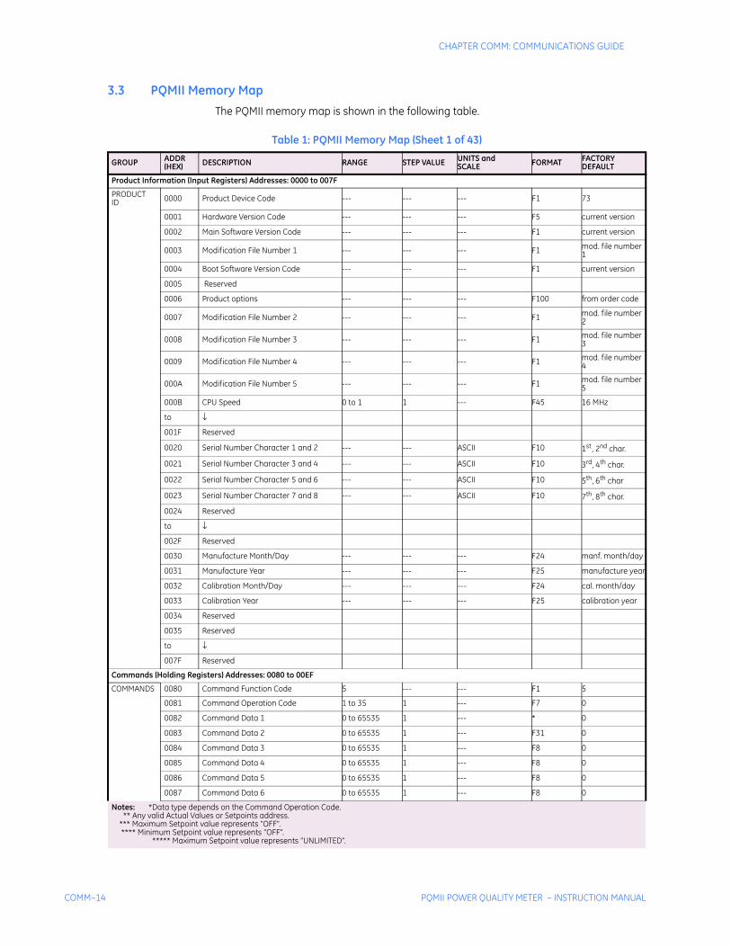
3.3 PQMII Memory MapThe PQMII memory map is shown in the following table.
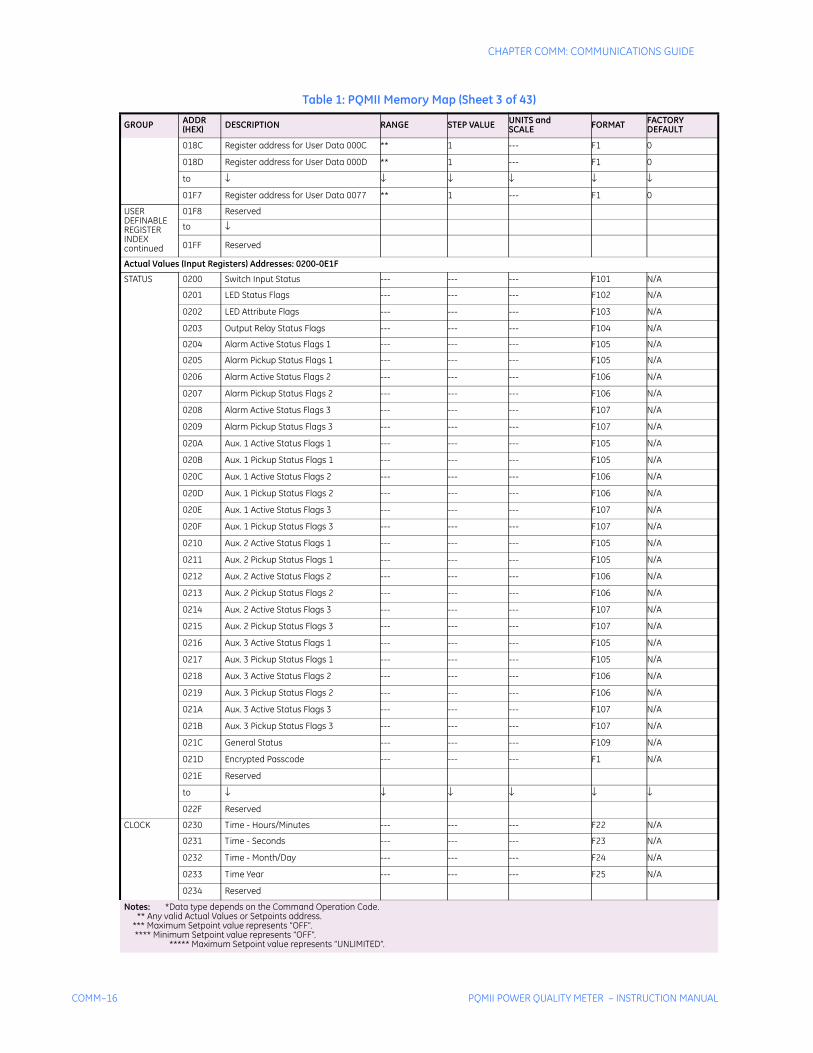
Table 1: PQMII Memory Map (Sheet 1 of 43)
GROUP ADDR(HEX) DESCRIPTION RANGE STEP VALUE UNITS and
SCALE FORMAT FACTORY DEFAULT
Product Information (Input Registers) Addresses: 0000 to 007F
PRODUCTID 0000 Product Device Code --- --- --- F1 73
0001 Hardware Version Code --- --- --- F5 current version
0002 Main Software Version Code --- --- --- F1 current version
0003 Modification File Number 1 --- --- --- F1 mod. file number 1
0004 Boot Software Version Code --- --- --- F1 current version
0005 Reserved
0006 Product options --- --- --- F100 from order code
0007 Modification File Number 2 --- --- --- F1 mod. file number 2
0008 Modification File Number 3 --- --- --- F1 mod. file number 3
0009 Modification File Number 4 --- --- --- F1 mod. file number 4
000A Modification File Number 5 --- --- --- F1 mod. file number 5
000B CPU Speed 0 to 1 1 --- F45 16 MHz
to ↓
001F Reserved
0020 Serial Number Character 1 and 2 --- --- ASCII F10 1st, 2nd char.
0021 Serial Number Character 3 and 4 --- --- ASCII F10 3rd, 4th char.
0022 Serial Number Character 5 and 6 --- --- ASCII F10 5th, 6th char
0023 Serial Number Character 7 and 8 --- --- ASCII F10 7th, 8th char.
0024 Reserved
to ↓
002F Reserved
0030 Manufacture Month/Day --- --- --- F24 manf. month/day
0031 Manufacture Year --- --- --- F25 manufacture year
0032 Calibration Month/Day --- --- --- F24 cal. month/day
0033 Calibration Year --- --- --- F25 calibration year
0034 Reserved
0035 Reserved
to ↓
007F Reserved
Commands (Holding Registers) Addresses: 0080 to 00EF
COMMANDS 0080 Command Function Code 5 --- --- F1 5
0081 Command Operation Code 1 to 35 1 --- F7 0
0082 Command Data 1 0 to 65535 1 --- * 0
0083 Command Data 2 0 to 65535 1 --- F31 0
0084 Command Data 3 0 to 65535 1 --- F8 0
0085 Command Data 4 0 to 65535 1 --- F8 0
0086 Command Data 5 0 to 65535 1 --- F8 0
0087 Command Data 6 0 to 65535 1 --- F8 0
Notes: *Data type depends on the Command Operation Code. ** Any valid Actual Values or Setpoints address. *** Maximum Setpoint value represents “OFF”. **** Minimum Setpoint value represents “OFF”. ***** Maximum Setpoint value represents “UNLIMITED”.
CHAPTER COMM: COMMUNICATIONS GUIDE
PQMII POWER QUALITY METER – INSTRUCTION MANUAL COMM–15
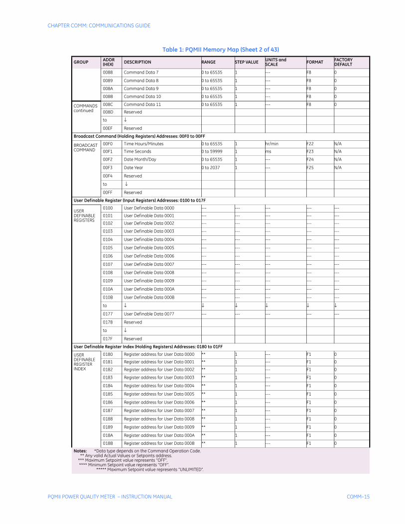
0088 Command Data 7 0 to 65535 1 --- F8 0
0089 Command Data 8 0 to 65535 1 --- F8 0
008A Command Data 9 0 to 65535 1 --- F8 0
008B Command Data 10 0 to 65535 1 --- F8 0
COMMANDS continued
008C Command Data 11 0 to 65535 1 --- F8 0
008D Reserved
to ↓
00EF Reserved
Broadcast Command (Holding Registers) Addresses: 00F0 to 00FF
BROADCASTCOMMAND
00F0 Time Hours/Minutes 0 to 65535 1 hr/min F22 N/A
00F1 Time Seconds 0 to 59999 1 ms F23 N/A
00F2 Date Month/Day 0 to 65535 1 --- F24 N/A
00F3 Date Year 0 to 2037 1 --- F25 N/A
00F4 Reserved
to ↓
00FF Reserved
User Definable Register (Input Registers) Addresses: 0100 to 017F
USERDEFINABLEREGISTERS
0100 User Definable Data 0000 --- --- --- --- ---
0101 User Definable Data 0001 --- --- --- --- ---
0102 User Definable Data 0002 --- --- --- --- ---
0103 User Definable Data 0003 --- --- --- --- ---
0104 User Definable Data 0004 --- --- --- --- ---
0105 User Definable Data 0005 --- --- --- --- ---
0106 User Definable Data 0006 --- --- --- --- ---
0107 User Definable Data 0007 --- --- --- --- ---
0108 User Definable Data 0008 --- --- --- --- ---
0109 User Definable Data 0009 --- --- --- --- ---
010A User Definable Data 000A --- --- --- --- ---
010B User Definable Data 000B --- --- --- --- ---
to ↓ ↓ ↓ ↓ ↓ ↓
0177 User Definable Data 0077 --- --- --- --- ---
0178 Reserved
to ↓
017F Reserved
User Definable Register Index (Holding Registers) Addresses: 0180 to 01FF
USERDEFINABLEREGISTERINDEX
0180 Register address for User Data 0000 ** 1 --- F1 0
0181 Register address for User Data 0001 ** 1 --- F1 0
0182 Register address for User Data 0002 ** 1 --- F1 0
0183 Register address for User Data 0003 ** 1 --- F1 0
0184 Register address for User Data 0004 ** 1 --- F1 0
0185 Register address for User Data 0005 ** 1 --- F1 0
0186 Register address for User Data 0006 ** 1 --- F1 0
0187 Register address for User Data 0007 ** 1 --- F1 0
0188 Register address for User Data 0008 ** 1 --- F1 0
0189 Register address for User Data 0009 ** 1 --- F1 0
018A Register address for User Data 000A ** 1 --- F1 0
018B Register address for User Data 000B ** 1 --- F1 0
Table 1: PQMII Memory Map (Sheet 2 of 43)
GROUP ADDR(HEX) DESCRIPTION RANGE STEP VALUE UNITS and
SCALE FORMAT FACTORY DEFAULT
Notes: *Data type depends on the Command Operation Code. ** Any valid Actual Values or Setpoints address. *** Maximum Setpoint value represents “OFF”. **** Minimum Setpoint value represents “OFF”. ***** Maximum Setpoint value represents “UNLIMITED”.
COMM–16 PQMII POWER QUALITY METER – INSTRUCTION MANUAL
CHAPTER COMM: COMMUNICATIONS GUIDE
018C Register address for User Data 000C ** 1 --- F1 0
018D Register address for User Data 000D ** 1 --- F1 0
to ↓ ↓ ↓ ↓ ↓ ↓
01F7 Register address for User Data 0077 ** 1 --- F1 0
USERDEFINABLEREGISTERINDEX continued
01F8 Reserved
to ↓
01FF Reserved
Actual Values (Input Registers) Addresses: 0200-0E1F
STATUS 0200 Switch Input Status --- --- --- F101 N/A
0201 LED Status Flags --- --- --- F102 N/A
0202 LED Attribute Flags --- --- --- F103 N/A
0203 Output Relay Status Flags --- --- --- F104 N/A
0204 Alarm Active Status Flags 1 --- --- --- F105 N/A
0205 Alarm Pickup Status Flags 1 --- --- --- F105 N/A
0206 Alarm Active Status Flags 2 --- --- --- F106 N/A
0207 Alarm Pickup Status Flags 2 --- --- --- F106 N/A
0208 Alarm Active Status Flags 3 --- --- --- F107 N/A
0209 Alarm Pickup Status Flags 3 --- --- --- F107 N/A
020A Aux. 1 Active Status Flags 1 --- --- --- F105 N/A
020B Aux. 1 Pickup Status Flags 1 --- --- --- F105 N/A
020C Aux. 1 Active Status Flags 2 --- --- --- F106 N/A
020D Aux. 1 Pickup Status Flags 2 --- --- --- F106 N/A
020E Aux. 1 Active Status Flags 3 --- --- --- F107 N/A
020F Aux. 1 Pickup Status Flags 3 --- --- --- F107 N/A
0210 Aux. 2 Active Status Flags 1 --- --- --- F105 N/A
0211 Aux. 2 Pickup Status Flags 1 --- --- --- F105 N/A
0212 Aux. 2 Active Status Flags 2 --- --- --- F106 N/A
0213 Aux. 2 Pickup Status Flags 2 --- --- --- F106 N/A
0214 Aux. 2 Active Status Flags 3 --- --- --- F107 N/A
0215 Aux. 2 Pickup Status Flags 3 --- --- --- F107 N/A
0216 Aux. 3 Active Status Flags 1 --- --- --- F105 N/A
0217 Aux. 3 Pickup Status Flags 1 --- --- --- F105 N/A
0218 Aux. 3 Active Status Flags 2 --- --- --- F106 N/A
0219 Aux. 3 Pickup Status Flags 2 --- --- --- F106 N/A
021A Aux. 3 Active Status Flags 3 --- --- --- F107 N/A
021B Aux. 3 Pickup Status Flags 3 --- --- --- F107 N/A
021C General Status --- --- --- F109 N/A
021D Encrypted Passcode --- --- --- F1 N/A
021E Reserved
to ↓ ↓ ↓ ↓ ↓ ↓
022F Reserved
CLOCK 0230 Time - Hours/Minutes --- --- --- F22 N/A
0231 Time - Seconds --- --- --- F23 N/A
0232 Time - Month/Day --- --- --- F24 N/A
0233 Time Year --- --- --- F25 N/A
0234 Reserved
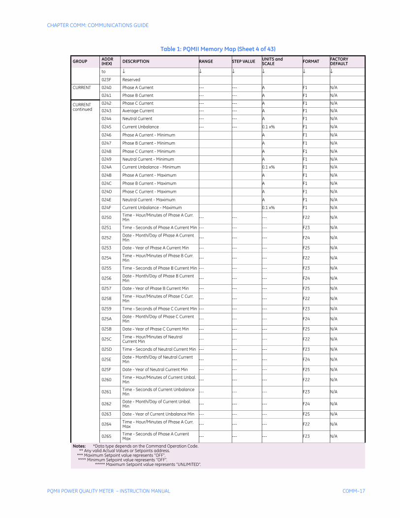
Table 1: PQMII Memory Map (Sheet 3 of 43)
GROUP ADDR(HEX) DESCRIPTION RANGE STEP VALUE UNITS and
SCALE FORMAT FACTORY DEFAULT
Notes: *Data type depends on the Command Operation Code. ** Any valid Actual Values or Setpoints address. *** Maximum Setpoint value represents “OFF”. **** Minimum Setpoint value represents “OFF”. ***** Maximum Setpoint value represents “UNLIMITED”.
CHAPTER COMM: COMMUNICATIONS GUIDE
PQMII POWER QUALITY METER – INSTRUCTION MANUAL COMM–17
to ↓ ↓ ↓ ↓ ↓ ↓
023F Reserved
CURRENT 0240 Phase A Current --- --- A F1 N/A
0241 Phase B Current --- --- A F1 N/A
CURRENTcontinued
0242 Phase C Current --- --- A F1 N/A
0243 Average Current --- --- A F1 N/A
0244 Neutral Current --- --- A F1 N/A
0245 Current Unbalance --- --- 0.1 x% F1 N/A
0246 Phase A Current - Minimum A F1 N/A
0247 Phase B Current - Minimum A F1 N/A
0248 Phase C Current - Minimum A F1 N/A
0249 Neutral Current - Minimum A F1 N/A
024A Current Unbalance - Minimum 0.1 x% F1 N/A
024B Phase A Current - Maximum A F1 N/A
024C Phase B Current - Maximum A F1 N/A
024D Phase C Current - Maximum A F1 N/A
024E Neutral Current - Maximum A F1 N/A
024F Current Unbalance - Maximum 0.1 x% F1 N/A
0250 Time - Hour/Minutes of Phase A Curr. Min --- --- --- F22 N/A
0251 Time - Seconds of Phase A Current Min --- --- --- F23 N/A
0252 Date - Month/Day of Phase A Current Min --- --- --- F24 N/A
0253 Date - Year of Phase A Current Min --- --- --- F25 N/A
0254 Time - Hour/Minutes of Phase B Curr. Min --- --- --- F22 N/A
0255 Time - Seconds of Phase B Current Min --- --- --- F23 N/A
0256 Date - Month/Day of Phase B Current Min --- --- --- F24 N/A
0257 Date - Year of Phase B Current Min --- --- --- F25 N/A
0258 Time - Hour/Minutes of Phase C Curr. Min --- --- --- F22 N/A
0259 Time - Seconds of Phase C Current Min --- --- --- F23 N/A
025A Date - Month/Day of Phase C Current Min --- --- --- F24 N/A
025B Date - Year of Phase C Current Min --- --- --- F25 N/A
025C Time - Hour/Minutes of Neutral Current Min --- --- --- F22 N/A
025D Time - Seconds of Neutral Current Min --- --- --- F23 N/A
025E Date - Month/Day of Neutral Current Min --- --- --- F24 N/A
025F Date - Year of Neutral Current Min --- --- --- F25 N/A
0260 Time - Hour/Minutes of Current Unbal. Min --- --- --- F22 N/A
0261 Time - Seconds of Current Unbalance Min --- --- --- F23 N/A
0262 Date - Month/Day of Current Unbal. Min --- --- --- F24 N/A
0263 Date - Year of Current Unbalance Min --- --- --- F25 N/A
0264 Time - Hour/Minutes of Phase A Curr. Max --- --- --- F22 N/A
0265 Time - Seconds of Phase A Current Max --- --- --- F23 N/A
Table 1: PQMII Memory Map (Sheet 4 of 43)
GROUP ADDR(HEX) DESCRIPTION RANGE STEP VALUE UNITS and
SCALE FORMAT FACTORY DEFAULT
Notes: *Data type depends on the Command Operation Code. ** Any valid Actual Values or Setpoints address. *** Maximum Setpoint value represents “OFF”. **** Minimum Setpoint value represents “OFF”. ***** Maximum Setpoint value represents “UNLIMITED”.
COMM–18 PQMII POWER QUALITY METER – INSTRUCTION MANUAL
CHAPTER COMM: COMMUNICATIONS GUIDE
0266 Date - Month/Day of Phase A Current Max --- --- --- F24 N/A
0267 Date - Year of Phase A Current Max --- --- --- F25 N/A
0268 Time - Hour/Minutes of Phase B Curr. Max --- --- --- F22 N/A
CURRENTcontinued 0269 Time - Seconds of Phase B Current
Max --- --- --- F23 N/A
026A Date - Month/Day of Phase B Current Max --- --- --- F24 N/A
026B Date - Year of Phase B Current Max --- --- --- F25 N/A
026C Time - Hour/Minutes of Phase C Curr. Max --- --- --- F22 N/A
026D Time - Seconds of Phase C Current Max --- --- --- F23 N/A
026E Date - Month/Day of Phase C Current Max --- --- --- F24 N/A
026F Date - Year of Phase C Current Max --- --- --- F25 N/A
0270 Time - Hour/Minutes of Neutral Current Max --- --- --- F22 N/A
0271 Time - Seconds of Neutral Current Max --- --- --- F23 N/A
0272 Date - Month/Day of Neutral Current Max --- --- --- F24 N/A
0273 Date - Year of Neutral Current Max --- --- --- F25 N/A
0274 Time - Hour/Minutes of Current Unbal. Max --- --- --- F22 N/A
0275 Time - Seconds of Current Unbal. Max --- --- --- F23 N/A
0276 Date - Month/Day of Current Unbal. Max --- --- --- F24 N/A
0277 Date - Year of Current Unbalance Max --- --- --- F25 N/A
0278 Reserved
to ↓ ↓ ↓ ↓ ↓ ↓
027F Reserved
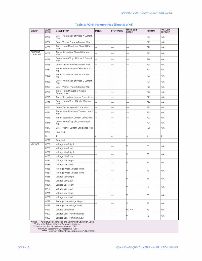
VOLTAGE 0280 Voltage Van (High)--- --- V F3 N/A
0281 Voltage Van (Low)
0282 Voltage Vbn (High)--- --- V F3 N/A
0283 Voltage Vbn (Low)
0284 Voltage Vcn (High)--- --- V F3 N/A
0285 Voltage Vcn (Low)
0286 Average Phase Voltage (High)--- --- V F3 N/A
0287 Average Phase Voltage (Low)
0288 Voltage Vab (High)--- --- V F3 N/A
0289 Voltage Vab (Low)
028A Voltage Vbc (High)--- --- V F3 N/A
028B Voltage Vbc (Low)
028C Voltage Vca (High)--- --- V F3 N/A
028D Voltage Vca (Low)
028E Average Line Voltage (High)--- --- V F3 N/A
028F Average Line Voltage (Low)
0290 Voltage Unbalance --- --- 0.1 x % F1 N/A
0291 Voltage Van - Minimum (high)--- --- V F3 N/A
0292 Voltage Van - Minimum (Low)
Table 1: PQMII Memory Map (Sheet 5 of 43)
GROUP ADDR(HEX) DESCRIPTION RANGE STEP VALUE UNITS and
SCALE FORMAT FACTORY DEFAULT
Notes: *Data type depends on the Command Operation Code. ** Any valid Actual Values or Setpoints address. *** Maximum Setpoint value represents “OFF”. **** Minimum Setpoint value represents “OFF”. ***** Maximum Setpoint value represents “UNLIMITED”.
CHAPTER COMM: COMMUNICATIONS GUIDE
PQMII POWER QUALITY METER – INSTRUCTION MANUAL COMM–19
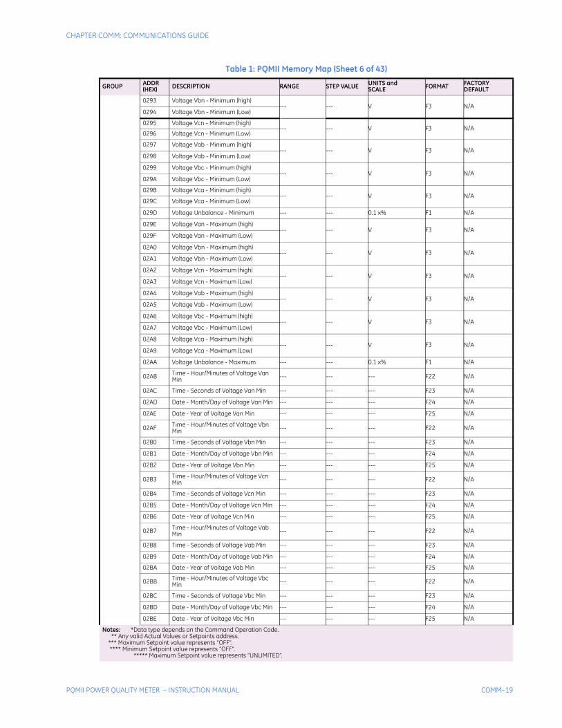
0293 Voltage Vbn - Minimum (high)--- --- V F3 N/A
0294 Voltage Vbn - Minimum (Low)
0295 Voltage Vcn - Minimum (high)--- --- V F3 N/A
0296 Voltage Vcn - Minimum (Low)
0297 Voltage Vab - Minimum (high)--- --- V F3 N/A
0298 Voltage Vab - Minimum (Low)
0299 Voltage Vbc - Minimum (high)--- --- V F3 N/A
029A Voltage Vbc - Minimum (Low)
029B Voltage Vca - Minimum (high)--- --- V F3 N/A
029C Voltage Vca - Minimum (Low)
029D Voltage Unbalance - Minimum --- --- 0.1 x% F1 N/A
029E Voltage Van - Maximum (high)--- --- V F3 N/A
029F Voltage Van - Maximum (Low)
02A0 Voltage Vbn - Maximum (high)--- --- V F3 N/A
02A1 Voltage Vbn - Maximum (Low)
02A2 Voltage Vcn - Maximum (high)--- --- V F3 N/A
02A3 Voltage Vcn - Maximum (Low)
02A4 Voltage Vab - Maximum (high)--- --- V F3 N/A
02A5 Voltage Vab - Maximum (Low)
02A6 Voltage Vbc - Maximum (high)--- --- V F3 N/A
02A7 Voltage Vbc - Maximum (Low)
02A8 Voltage Vca - Maximum (high)--- --- V F3 N/A
02A9 Voltage Vca - Maximum (Low)
02AA Voltage Unbalance - Maximum --- --- 0.1 x% F1 N/A
02AB Time - Hour/Minutes of Voltage Van Min --- --- --- F22 N/A
02AC Time - Seconds of Voltage Van Min --- --- --- F23 N/A
02AD Date - Month/Day of Voltage Van Min --- --- --- F24 N/A
02AE Date - Year of Voltage Van Min --- --- --- F25 N/A
02AF Time - Hour/Minutes of Voltage Vbn Min --- --- --- F22 N/A
02B0 Time - Seconds of Voltage Vbn Min --- --- --- F23 N/A
02B1 Date - Month/Day of Voltage Vbn Min --- --- --- F24 N/A
02B2 Date - Year of Voltage Vbn Min --- --- --- F25 N/A
02B3 Time - Hour/Minutes of Voltage Vcn Min --- --- --- F22 N/A
02B4 Time - Seconds of Voltage Vcn Min --- --- --- F23 N/A
02B5 Date - Month/Day of Voltage Vcn Min --- --- --- F24 N/A
02B6 Date - Year of Voltage Vcn Min --- --- --- F25 N/A
02B7 Time - Hour/Minutes of Voltage Vab Min --- --- --- F22 N/A
02B8 Time - Seconds of Voltage Vab Min --- --- --- F23 N/A
02B9 Date - Month/Day of Voltage Vab Min --- --- --- F24 N/A
02BA Date - Year of Voltage Vab Min --- --- --- F25 N/A
02BB Time - Hour/Minutes of Voltage Vbc Min --- --- --- F22 N/A
02BC Time - Seconds of Voltage Vbc Min --- --- --- F23 N/A
02BD Date - Month/Day of Voltage Vbc Min --- --- --- F24 N/A
02BE Date - Year of Voltage Vbc Min --- --- --- F25 N/A
Table 1: PQMII Memory Map (Sheet 6 of 43)
GROUP ADDR(HEX) DESCRIPTION RANGE STEP VALUE UNITS and
SCALE FORMAT FACTORY DEFAULT
Notes: *Data type depends on the Command Operation Code. ** Any valid Actual Values or Setpoints address. *** Maximum Setpoint value represents “OFF”. **** Minimum Setpoint value represents “OFF”. ***** Maximum Setpoint value represents “UNLIMITED”.
COMM–20 PQMII POWER QUALITY METER – INSTRUCTION MANUAL
CHAPTER COMM: COMMUNICATIONS GUIDE
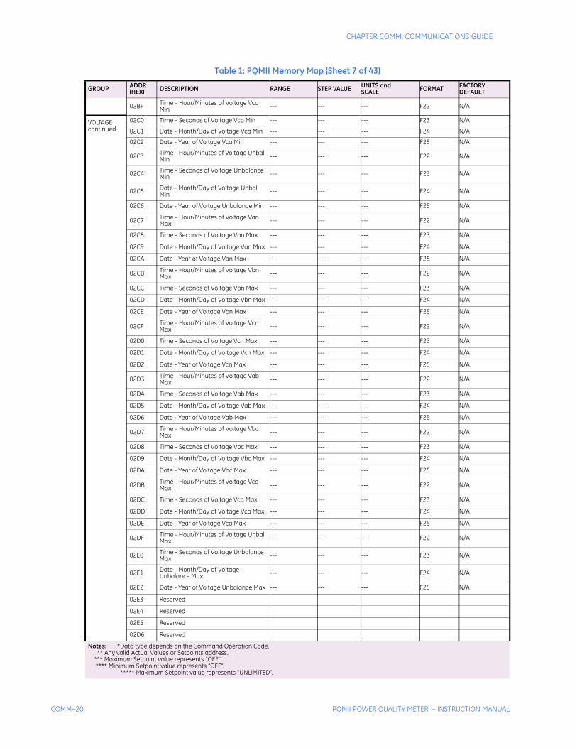
02BF Time - Hour/Minutes of Voltage Vca Min --- --- --- F22 N/A
VOLTAGEcontinued
02C0 Time - Seconds of Voltage Vca Min --- --- --- F23 N/A
02C1 Date - Month/Day of Voltage Vca Min --- --- --- F24 N/A
02C2 Date - Year of Voltage Vca Min --- --- --- F25 N/A
02C3 Time - Hour/Minutes of Voltage Unbal. Min --- --- --- F22 N/A
02C4 Time - Seconds of Voltage Unbalance Min --- --- --- F23 N/A
02C5 Date - Month/Day of Voltage Unbal. Min --- --- --- F24 N/A
02C6 Date - Year of Voltage Unbalance Min --- --- --- F25 N/A
02C7 Time - Hour/Minutes of Voltage Van Max --- --- --- F22 N/A
02C8 Time - Seconds of Voltage Van Max --- --- --- F23 N/A
02C9 Date - Month/Day of Voltage Van Max --- --- --- F24 N/A
02CA Date - Year of Voltage Van Max --- --- --- F25 N/A
02CB Time - Hour/Minutes of Voltage Vbn Max --- --- --- F22 N/A
02CC Time - Seconds of Voltage Vbn Max --- --- --- F23 N/A
02CD Date - Month/Day of Voltage Vbn Max --- --- --- F24 N/A
02CE Date - Year of Voltage Vbn Max --- --- --- F25 N/A
02CF Time - Hour/Minutes of Voltage Vcn Max --- --- --- F22 N/A
02D0 Time - Seconds of Voltage Vcn Max --- --- --- F23 N/A
02D1 Date - Month/Day of Voltage Vcn Max --- --- --- F24 N/A
02D2 Date - Year of Voltage Vcn Max --- --- --- F25 N/A
02D3 Time - Hour/Minutes of Voltage Vab Max --- --- --- F22 N/A
02D4 Time - Seconds of Voltage Vab Max --- --- --- F23 N/A
02D5 Date - Month/Day of Voltage Vab Max --- --- --- F24 N/A
02D6 Date - Year of Voltage Vab Max --- --- --- F25 N/A
02D7 Time - Hour/Minutes of Voltage Vbc Max --- --- --- F22 N/A
02D8 Time - Seconds of Voltage Vbc Max --- --- --- F23 N/A
02D9 Date - Month/Day of Voltage Vbc Max --- --- --- F24 N/A
02DA Date - Year of Voltage Vbc Max --- --- --- F25 N/A
02DB Time - Hour/Minutes of Voltage Vca Max --- --- --- F22 N/A
02DC Time - Seconds of Voltage Vca Max --- --- --- F23 N/A
02DD Date - Month/Day of Voltage Vca Max --- --- --- F24 N/A
02DE Date - Year of Voltage Vca Max --- --- --- F25 N/A
02DF Time - Hour/Minutes of Voltage Unbal. Max --- --- --- F22 N/A
02E0 Time - Seconds of Voltage Unbalance Max --- --- --- F23 N/A
02E1 Date - Month/Day of Voltage Unbalance Max --- --- --- F24 N/A
02E2 Date - Year of Voltage Unbalance Max --- --- --- F25 N/A
02E3 Reserved
02E4 Reserved
02E5 Reserved
02D6 Reserved
Table 1: PQMII Memory Map (Sheet 7 of 43)
GROUP ADDR(HEX) DESCRIPTION RANGE STEP VALUE UNITS and
SCALE FORMAT FACTORY DEFAULT
Notes: *Data type depends on the Command Operation Code. ** Any valid Actual Values or Setpoints address. *** Maximum Setpoint value represents “OFF”. **** Minimum Setpoint value represents “OFF”. ***** Maximum Setpoint value represents “UNLIMITED”.
CHAPTER COMM: COMMUNICATIONS GUIDE
PQMII POWER QUALITY METER – INSTRUCTION MANUAL COMM–21
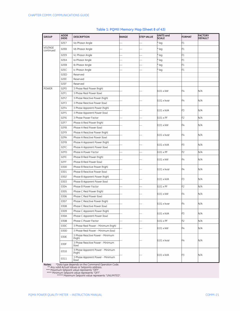
02E7 Va Phasor Angle --- --- ° lag F1
VOLTAGEcontinued 02E8 Vb Phasor Angle --- --- ° lag F1
02E9 Vc Phasor Angle --- --- ° lag F1
02EA Ia Phasor Angle --- --- ° lag F1
02EB Ib Phasor Angle --- --- ° lag F1
02EC Ic Phasor Angle --- --- ° lag F1
02ED Reserved
02EE Reserved
02EF Reserved
POWER 02F0 3 Phase Real Power (high)--- --- 0.01 x kW F4 N/A
02F1 3 Phase Real Power (low)
02F2 3 Phase Reactive Power (high)--- --- 0.01 x kvar F4 N/A
02F3 3 Phase Reactive Power (low)
02F4 3 Phase Apparent Power (high)--- --- 0.01 x kVA F3 N/A
02F5 3 Phase Apparent Power (low)
02F6 3 Phase Power Factor --- --- 0.01 x PF F2 N/A
02F7 Phase A Real Power (high)--- --- 0.01 x kW F4 N/A
02F8 Phase A Real Power (low)
02F9 Phase A Reactive Power (high)--- --- 0.01 x kvar F4 N/A
02FA Phase A Reactive Power (low)
02FB Phase A Apparent Power (high)--- --- 0.01 x kVA F3 N/A
02FC Phase A Apparent Power (low)
02FD Phase A Power Factor --- --- 0.01 x PF F2 N/A
02FE Phase B Real Power (high)--- --- 0.01 x kW F4 N/A
02FF Phase B Real Power (low)
0300 Phase B Reactive Power (high)--- --- 0.01 x kvar F4 N/A
0301 Phase B Reactive Power (low)
0302 Phase B Apparent Power (high)--- --- 0.01 x kVA F3 N/A
0303 Phase B Apparent Power (low)
0304 Phase B Power Factor --- --- 0.01 x PF F2 N/A
0305 Phase C Real Power (high)--- --- 0.01 x kW F4 N/A
0306 Phase C Real Power (low)
0307 Phase C Reactive Power (high)--- --- 0.01 x kvar F4 N/A
0308 Phase C Reactive Power (low)
0309 Phase C Apparent Power (high)--- --- 0.01 x kVA F3 N/A
030A Phase C Apparent Power (low)
030B Phase C Power Factor --- --- 0.01 x PF F2 N/A
030C 3 Phase Real Power - Minimum (high)--- --- 0.01 x kW F4 N/A
030D 3 Phase Real Power - Minimum (low)
030E 3 Phase Reactive Power - Minimum (high)
--- --- 0.01 x kvar F4 N/A030F 3 Phase Reactive Power - Minimum
(low)
0310 3 Phase Apparent Power - Minimum (high)
--- --- 0.01 x kVA F3 N/A0311 3 Phase Apparent Power - Minimum
(low)
Table 1: PQMII Memory Map (Sheet 8 of 43)
GROUP ADDR(HEX) DESCRIPTION RANGE STEP VALUE UNITS and
SCALE FORMAT FACTORY DEFAULT
Notes: *Data type depends on the Command Operation Code. ** Any valid Actual Values or Setpoints address. *** Maximum Setpoint value represents “OFF”. **** Minimum Setpoint value represents “OFF”. ***** Maximum Setpoint value represents “UNLIMITED”.
COMM–22 PQMII POWER QUALITY METER – INSTRUCTION MANUAL
CHAPTER COMM: COMMUNICATIONS GUIDE
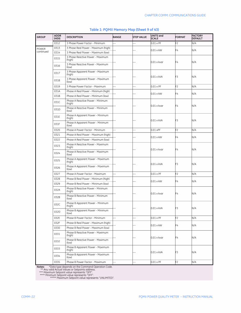
0312 3 Phase Power Factor - Minimum --- --- 0.01 x PF F2 N/A
POWERcontinued
0313 3 Phase Real Power - Maximum (high)--- --- 0.01 x kW F4 N/A
0314 3 Phase Real Power - Maximum (low)
0315 3 Phase Reactive Power - Maximum (high)
--- --- 0.01 x kvar F4 N/A0316 3 Phase Reactive Power - Maximum
(low)
0317 3 Phase Apparent Power - Maximum (high)
--- --- 0.01 x kVA F3 N/A0318 3 Phase Apparent Power - Maximum
(low)
0319 3 Phase Power Factor - Maximum --- --- 0.01 x PF F2 N/A
031A Phase A Real Power - Minimum (high)--- --- 0.01 x kW F4 N/A
031B Phase A Real Power - Minimum (low)
031C Phase A Reactive Power - Minimum (high)
--- --- 0.01 x kvar F4 N/A031D Phase A Reactive Power - Minimum
(low)
031E Phase A Apparent Power - Minimum (high)
--- --- 0.01 x kVA F3 N/A031F Phase A Apparent Power - Minimum
(low)
0320 Phase A Power Factor - Minimum --- --- 0.01 xPF F2 N/A
0321 Phase A Real Power - Maximum (high)--- --- 0.01 x kW F4 N/A
0322 Phase A Real Power - Maximum (low)
0323 Phase A Reactive Power - Maximum (high)
--- --- 0.01 x kvar F4 N/A0324 Phase A Reactive Power - Maximum
(low)
0325 Phase A Apparent Power - Maximum (high)
--- --- 0.01 x kVA F3 N/A0326 Phase A Apparent Power - Maximum
(low)
0327 Phase A Power Factor - Maximum --- --- 0.01 x PF F2 N/A
0328 Phase B Real Power - Minimum (high)--- --- 0.01 x kW F4 N/A
0329 Phase B Real Power - Minimum (low)
032A Phase B Reactive Power - Minimum (high)
--- --- 0.01 x kvar F4 N/A032B Phase B Reactive Power - Minimum
(low)
032C Phase B Apparent Power - Minimum (high)
--- --- 0.01 x kVA F3 N/A032D Phase B Apparent Power - Minimum
(low)
032E Phase B Power Factor - Minimum --- --- 0.01 x PF F2 N/A
032F Phase B Real Power - Maximum (high)--- --- 0.01 x kW F4 N/A
0330 Phase B Real Power - Maximum (low)
0331 Phase B Reactive Power - Maximum (high)
--- --- 0.01 x kvar F4 N/A0332 Phase B Reactive Power - Maximum
(low)
0333 Phase B Apparent Power - Maximum (high)
--- --- 0.01 x kVA F3 N/A0334 Phase B Apparent Power - Maximum
(low)
0335 Phase B Power Factor - Maximum --- --- 0.01 x PF F2 N/A
Table 1: PQMII Memory Map (Sheet 9 of 43)
GROUP ADDR(HEX) DESCRIPTION RANGE STEP VALUE UNITS and
SCALE FORMAT FACTORY DEFAULT
Notes: *Data type depends on the Command Operation Code. ** Any valid Actual Values or Setpoints address. *** Maximum Setpoint value represents “OFF”. **** Minimum Setpoint value represents “OFF”. ***** Maximum Setpoint value represents “UNLIMITED”.
CHAPTER COMM: COMMUNICATIONS GUIDE
PQMII POWER QUALITY METER – INSTRUCTION MANUAL COMM–23
POWERcontinued
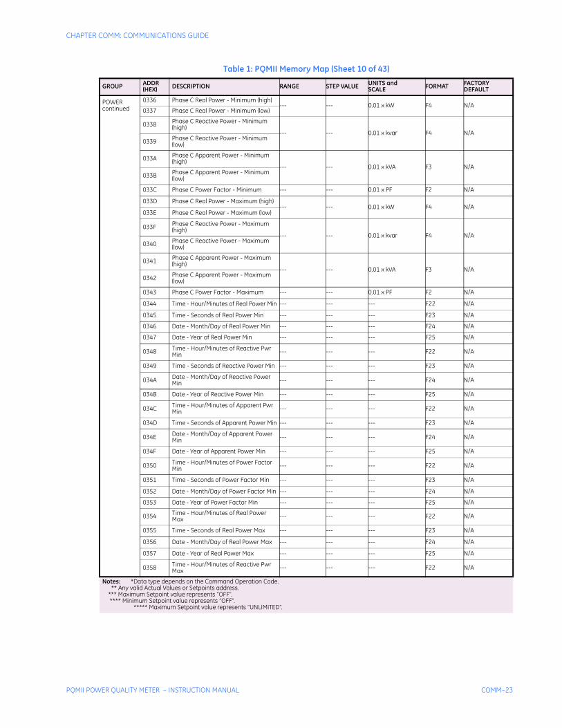
0336 Phase C Real Power - Minimum (high)--- --- 0.01 x kW F4 N/A
0337 Phase C Real Power - Minimum (low)
0338 Phase C Reactive Power - Minimum (high)
--- --- 0.01 x kvar F4 N/A0339 Phase C Reactive Power - Minimum
(low)
033A Phase C Apparent Power - Minimum (high)
--- --- 0.01 x kVA F3 N/A033B Phase C Apparent Power - Minimum
(low)
033C Phase C Power Factor - Minimum --- --- 0.01 x PF F2 N/A
033D Phase C Real Power - Maximum (high)--- --- 0.01 x kW F4 N/A
033E Phase C Real Power - Maximum (low)
033F Phase C Reactive Power - Maximum (high)
--- --- 0.01 x kvar F4 N/A0340 Phase C Reactive Power - Maximum
(low)
0341 Phase C Apparent Power - Maximum (high)
--- --- 0.01 x kVA F3 N/A0342 Phase C Apparent Power - Maximum
(low)
0343 Phase C Power Factor - Maximum --- --- 0.01 x PF F2 N/A
0344 Time - Hour/Minutes of Real Power Min --- --- --- F22 N/A
0345 Time - Seconds of Real Power Min --- --- --- F23 N/A
0346 Date - Month/Day of Real Power Min --- --- --- F24 N/A
0347 Date - Year of Real Power Min --- --- --- F25 N/A
0348 Time - Hour/Minutes of Reactive Pwr Min --- --- --- F22 N/A
0349 Time - Seconds of Reactive Power Min --- --- --- F23 N/A
034A Date - Month/Day of Reactive Power Min --- --- --- F24 N/A
034B Date - Year of Reactive Power Min --- --- --- F25 N/A
034C Time - Hour/Minutes of Apparent Pwr Min --- --- --- F22 N/A
034D Time - Seconds of Apparent Power Min --- --- --- F23 N/A
034E Date - Month/Day of Apparent Power Min --- --- --- F24 N/A
034F Date - Year of Apparent Power Min --- --- --- F25 N/A
0350 Time - Hour/Minutes of Power Factor Min --- --- --- F22 N/A
0351 Time - Seconds of Power Factor Min --- --- --- F23 N/A
0352 Date - Month/Day of Power Factor Min --- --- --- F24 N/A
0353 Date - Year of Power Factor Min --- --- --- F25 N/A
0354 Time - Hour/Minutes of Real Power Max --- --- --- F22 N/A
0355 Time - Seconds of Real Power Max --- --- --- F23 N/A
0356 Date - Month/Day of Real Power Max --- --- --- F24 N/A
0357 Date - Year of Real Power Max --- --- --- F25 N/A
0358 Time - Hour/Minutes of Reactive Pwr Max --- --- --- F22 N/A
Table 1: PQMII Memory Map (Sheet 10 of 43)
GROUP ADDR(HEX) DESCRIPTION RANGE STEP VALUE UNITS and
SCALE FORMAT FACTORY DEFAULT
Notes: *Data type depends on the Command Operation Code. ** Any valid Actual Values or Setpoints address. *** Maximum Setpoint value represents “OFF”. **** Minimum Setpoint value represents “OFF”. ***** Maximum Setpoint value represents “UNLIMITED”.
COMM–24 PQMII POWER QUALITY METER – INSTRUCTION MANUAL
CHAPTER COMM: COMMUNICATIONS GUIDE
POWERcontinued 0359 Time - Seconds of Reactive Power Max --- --- --- F23 N/A
035A Date - Month/Day of Reactive Pwr Max --- --- --- F24 N/A
035B Date - Year of Reactive Power Max --- --- --- F25 N/A
035C Time - Hour/Minutes of Apparent Pwr Max --- --- --- F22 N/A
035D Time - Seconds of Apparent Pwr Max --- --- --- F23 N/A
035E Date - Month/Day of Apparent Pwr Max --- --- --- F24 N/A
035F Date - Year of Apparent Power Max --- --- --- F25 N/A
0360 Time - Hour/Minutes of Power Factor Max --- --- --- F22 N/A
0361 Time - Seconds of Power Factor Max --- --- --- F23 N/A
0362 Date - Month/Day of Power Factor Max --- --- --- F24 N/A
0363 Date - Year of Power Factor Max --- --- --- F25 N/A
0364 Time - Hour/Min of Phase A Real Pwr Min --- --- --- F22 N/A
0365 Time - Seconds of Phase A Real Pwr Min --- --- --- F23 N/A
0366 Date - Month/Day of Phase A Real Pwr Min --- --- --- F24 N/A
0367 Date - Year of Phase A Real Pwr Min --- --- --- F25 N/A
0368 Time - Hour/Min of Phase A React Pwr Min --- --- --- F22 N/A
0369 Time - Seconds of Phase A React Pwr Min --- --- --- F23 N/A
036A Date - Month/Day of Phase A React Pwr Min --- --- --- F24 N/A
036B Date - Year of Phase A Reactive Pwr Min --- --- --- F25 N/A
036C Time - Hour/Min of Phase A App Pwr Min --- --- --- F22 N/A
036D Time - Seconds of Phase A App Pwr Min --- --- --- F23 N/A
036E Date - Month/Day of Phase A App Pwr Min --- --- --- F24 N/A
036F Date - Year of Phase A Apparent Pwr Min --- --- --- F25 N/A
0370 Time - Hour/Minutes of Phase A PF Min --- --- --- F22 N/A
0371 Time - Seconds of Phase A PF Min --- --- --- F23 N/A
0372 Date - Month/Day of Phase A PF Min --- --- --- F24 N/A
0373 Date - Year of Phase A Power Factor Min --- --- --- F25 N/A
0374 Time - Hour/Min of Phase A Real Pwr Max --- --- --- F22 N/A
0375 Time - Seconds of Phase A Real Pwr Max --- --- --- F23 N/A
0376 Date - Month/Day of Phase A Real Pwr Max --- --- --- F24 N/A
0377 Date - Year of Phase A Real Power Max --- --- --- F25 N/A
0378 Time - Hour/Min of Phase A React Pwr Max --- --- --- F22 N/A
0379 Time - Seconds of Phase A React Pwr Max --- --- --- F23 N/A
037A Date - Mnth/Day of Phase A React Pwr Max --- --- --- F24 N/A
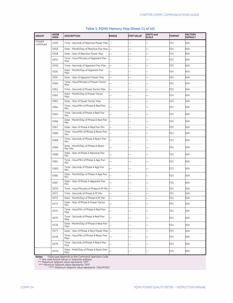
Table 1: PQMII Memory Map (Sheet 11 of 43)
GROUP ADDR(HEX) DESCRIPTION RANGE STEP VALUE UNITS and
SCALE FORMAT FACTORY DEFAULT
Notes: *Data type depends on the Command Operation Code. ** Any valid Actual Values or Setpoints address. *** Maximum Setpoint value represents “OFF”. **** Minimum Setpoint value represents “OFF”. ***** Maximum Setpoint value represents “UNLIMITED”.
CHAPTER COMM: COMMUNICATIONS GUIDE
PQMII POWER QUALITY METER – INSTRUCTION MANUAL COMM–25
POWERcontinued 037B Date - Year of Phase A Reactive Pwr
Max --- --- --- F25 N/A
037C Time - Hour/Min of Phase A App Pwr Max --- --- --- F22 N/A
037D Time - Seconds of Phase A App Pwr Max --- --- --- F23 N/A
037E Date - Month/Day of Phase A App Pwr Max --- --- --- F24 N/A
037F Date - Year of Phase A Apparent Pwr Max --- --- --- F25 N/A
0380 Time - Hour/Minutes of Phase A PF Max --- --- --- F22 N/A
0381 Time - Seconds of Phase A PF Max --- --- --- F23 N/A
0382 Date - Month/Day of Phase A PF Max --- --- --- F24 N/A
0383 Date - Year of Phase A Power Factor Max --- --- --- F25 N/A
0384 Time - Hour/Min of Phase B Real Pwr Min --- --- --- F22 N/A
0385 Time - Seconds of Phase B Real Pwr Min --- --- --- F23 N/A
0386 Date - Month/Day of Phase B Real Pwr Min --- --- --- F24 N/A
0387 Date - Year of Phase B Real Power Min --- --- --- F25 N/A
0388 Time - Hour/Min of Phase B React Pwr Min --- --- --- F22 N/A
0389 Time - Seconds of Phase B React Pwr Min --- --- --- F23 N/A
038A Date - Month/Day of Phase B React Pwr Min --- --- --- F24 N/A
038B Date - Year of Phase B Reactive Pwr Min --- --- --- F25 N/A
038C Time - Hour/Min of Phase B App Pwr Min --- --- --- F22 N/A
038D Time - Seconds of Phase B App Pwr Min --- --- --- F23 N/A
038E Date - Month/Day of Phase B App Pwr Min --- --- --- F24 N/A
038F Date - Year of Phase B Apparent Pwr Min --- --- --- F25 N/A
0390 Time - Hour/Minutes of Phase B PF Min --- --- --- F22 N/A
0391 Time - Seconds of Phase B PF Min --- --- --- F23 N/A
0392 Date - Month/Day of Phase B PF Min --- --- --- F24 N/A
0393 Date - Year of Phase B PF Min --- --- --- F25 N/A
0394 Time - Hour/Min of Phase B Real Pwr Max --- --- --- F22 N/A
0395 Time - Seconds of Phase B Real Pwr Max --- --- --- F23 N/A
0396 Date - Month/Day of Phase B Real Pwr Max --- --- --- F24 N/A
0397 Date - Year of Phase B Real Power Max --- --- --- F25 N/A
0398 Time - Hour/Min of Phase B React Pwr Max --- --- --- F22 N/A
0399 Time - Seconds of Phase B React Pwr Max --- --- --- F23 N/A
039A Date - Mnth/Day of Phase B React Pwr Max --- --- --- F24 N/A
039B Date - Year of Phase B Reactive Pwr Max --- --- --- F25 N/A
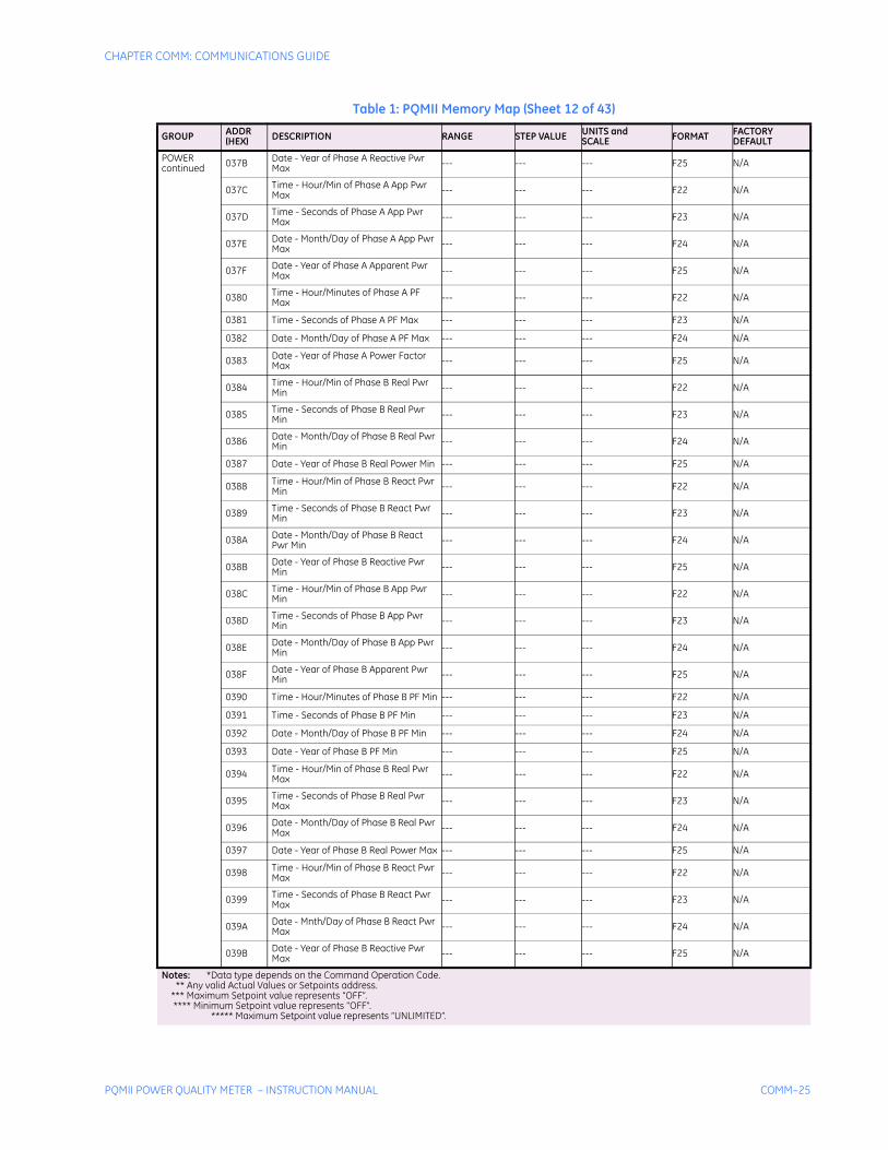
Table 1: PQMII Memory Map (Sheet 12 of 43)
GROUP ADDR(HEX) DESCRIPTION RANGE STEP VALUE UNITS and
SCALE FORMAT FACTORY DEFAULT
Notes: *Data type depends on the Command Operation Code. ** Any valid Actual Values or Setpoints address. *** Maximum Setpoint value represents “OFF”. **** Minimum Setpoint value represents “OFF”. ***** Maximum Setpoint value represents “UNLIMITED”.
COMM–26 PQMII POWER QUALITY METER – INSTRUCTION MANUAL
CHAPTER COMM: COMMUNICATIONS GUIDE
POWERcontinued 039C Time - Hour/Min of Phase B App Pwr
Max --- --- --- F22 N/A
039D Time - Seconds of Phase B App Pwr Max --- --- --- F23 N/A
039E Date - Month/Day of Phase B App Pwr Max --- --- --- F24 N/A
039F Date - Year of Phase B Apparent Pwr Max --- --- --- F25 N/A
03A0 Time - Hour/Minutes of Phase B PF Max --- --- --- F22 N/A
03A1 Time - Seconds of Phase B PF Max --- --- --- F23 N/A
03A2 Date - Month/Day of Phase B PF Max --- --- --- F24 N/A
03A3 Date - Year of Phase B Power Factor Max --- --- --- F25 N/A
03A4 Time - Hour/Min of Phase C Real Pwr Min --- --- --- F22 N/A
03A5 Time - Seconds of Phase C Real Pwr Min --- --- --- F23 N/A
03A6 Date - Month/Day of Phase C Real Pwr Min --- --- --- F24 N/A
03A7 Date - Year of Phase C Real Power Min --- --- --- F25 N/A
03A8 Time - Hour/Min of Phase C React Pwr Min --- --- --- F22 N/A
03A9 Time - Seconds of Phase C React Pwr Min --- --- --- F23 N/A
03AA Date - Mnth/Day of Phase C React Pwr Min --- --- --- F24 N/A
03AB Date - Year of Phase C Reactive Pwr Min --- --- --- F25 N/A
03AC Time - Hour/Min of Phase C App Pwr Min --- --- --- F22 N/A
03AD Time - Seconds of Phase C App Pwr Min --- --- --- F23 N/A
03AE Date - Month/Day of Phase C App Pwr Min --- --- --- F24 N/A
03AF Date - Year of Phase C Apparent Pwr Min --- --- --- F25 N/A
03B0 Time - Hour/Minutes of Phase C PF Min --- --- --- F22 N/A
03B1 Time - Seconds of Phase C PF Min --- --- --- F23 N/A
03B2 Date - Month/Day of Phase C PF Min --- --- --- F24 N/A
03B3 Date - Year of Phase C Power Factor Min --- --- --- F25 N/A
03B4 Time - Hour/Min of Phase C Real Pwr Max --- --- --- F22 N/A
03B5 Time - Seconds of Phase C Real Pwr Max --- --- --- F23 N/A
03B6 Date - Month/Day of Phase C Real Pwr Max --- --- --- F24 N/A
03B7 Date - Year of Phase C Real Power Max --- --- --- F25 N/A
03B8 Time - Hour/Min of Phase C React Pwr Max --- --- --- F22 N/A
03B9 Time - Seconds of Phase C React Pwr Max --- --- --- F23 N/A
03BA Date - Mnth/Day of Phase C React Pwr Max --- --- --- F24 N/A
03BB Date - Year of Phase C Reactive Pwr Max --- --- --- F25 N/A
03BC Time - Hour/Min of Phase C App Pwr Max --- --- --- F22 N/A
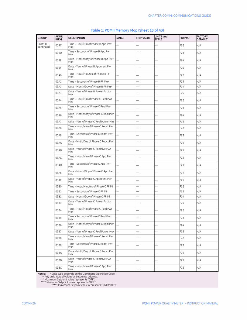
Table 1: PQMII Memory Map (Sheet 13 of 43)
GROUP ADDR(HEX) DESCRIPTION RANGE STEP VALUE UNITS and
SCALE FORMAT FACTORY DEFAULT
Notes: *Data type depends on the Command Operation Code. ** Any valid Actual Values or Setpoints address. *** Maximum Setpoint value represents “OFF”. **** Minimum Setpoint value represents “OFF”. ***** Maximum Setpoint value represents “UNLIMITED”.
CHAPTER COMM: COMMUNICATIONS GUIDE
PQMII POWER QUALITY METER – INSTRUCTION MANUAL COMM–27
POWERcontinued 03BD Time - Seconds of Phase C App Pwr
Max --- --- --- F23 N/A
03BE Date - Month/Day of Phase C App Pwr Max --- --- --- F24 N/A
03BF Date - Year of Phase C Apparent Pwr Max --- --- --- F25 N/A
03C0 Time - Hour/Minutes of Phase C PF Max --- --- --- F22 N/A
03C1 Time - Seconds of Phase C PF Max --- --- --- F23 N/A
03C2 Date - Month/Day of Phase C PF Max --- --- --- F24 N/A
03C3 Date - Year of Phase C Power Factor Max --- --- --- F25 N/A
03C4 Reserved
to ↓ ↓ ↓ ↓ ↓ ↓
03CF Reserved
ENERGY 03D0 3 Phase Positive Real Energy Used (high)
--- --- kWh F3 N/A03D1 3 Phase Positive Real Energy Used
(low)
03D2 3 Phase Negative Real Energy Used (high)
--- --- kWh F3 N/A03D3 3 Phase Negative Real Energy Used
(low)
03D4 3 Phase Positive React. Energy Used (high)
--- --- kvarh F3 N/A03D5 3 Phase Positive React. Energy Used
(low)
03D6 3 Phase Neg Reactive Energy Used (high)
--- --- kvarh F3 N/A03D7 3 Phase Neg Reactive Energy Used
(low)
03D8 3 Phase Apparent Energy Used (high)--- --- kVAh F3 N/A
03D9 3 Phase Apparent Energy Used (low)
03DA 3 Phase Energy Used in Last 24 h (high)--- --- kWh F3 N/A
03DB 3 Phase Energy Used in Last 24 h (low)
03DC 3 Phase Energy Cost Since Reset (high)--- --- $ x 0.01 F3 N/A
03DD 3 Phase Energy Cost Since Reset (low)
03DE 3 Phase Energy Cost Per Day (high)--- --- $ x 0.01 F3 N/A
03DF 3 Phase Energy Cost Per Day (low)
03E0 Time - Hours/Minutes of Last Reset --- --- --- F22 N/A
03E1 Time - Seconds of Last Reset --- --- --- F23 N/A
03E2 Date - Month/Day of Last Reset --- --- --- F24 N/A
03E3 Date - Year of Last Reset --- --- --- F25 N/A
03E4 Tariff Period 1 Positive Real Energy (high)
--- --- kWh F3 N/A03E5 Tariff Period 1 Positive Real Energy
(low)
03E6 Tariff Period 1 Negative Real Energy (high)
--- --- kWh F3 N/A03E7 Tariff Period 1 Negative Real Energy
(low)
03E8 Tariff Period 2 Positive Real Energy (high)
--- --- kWh F3 N/A03E9 Tariff Period 2 Positive Real Energy
(low)
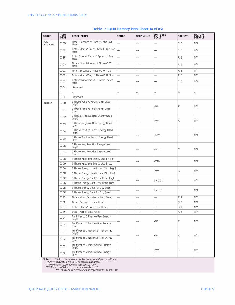
Table 1: PQMII Memory Map (Sheet 14 of 43)
GROUP ADDR(HEX) DESCRIPTION RANGE STEP VALUE UNITS and
SCALE FORMAT FACTORY DEFAULT
Notes: *Data type depends on the Command Operation Code. ** Any valid Actual Values or Setpoints address. *** Maximum Setpoint value represents “OFF”. **** Minimum Setpoint value represents “OFF”. ***** Maximum Setpoint value represents “UNLIMITED”.
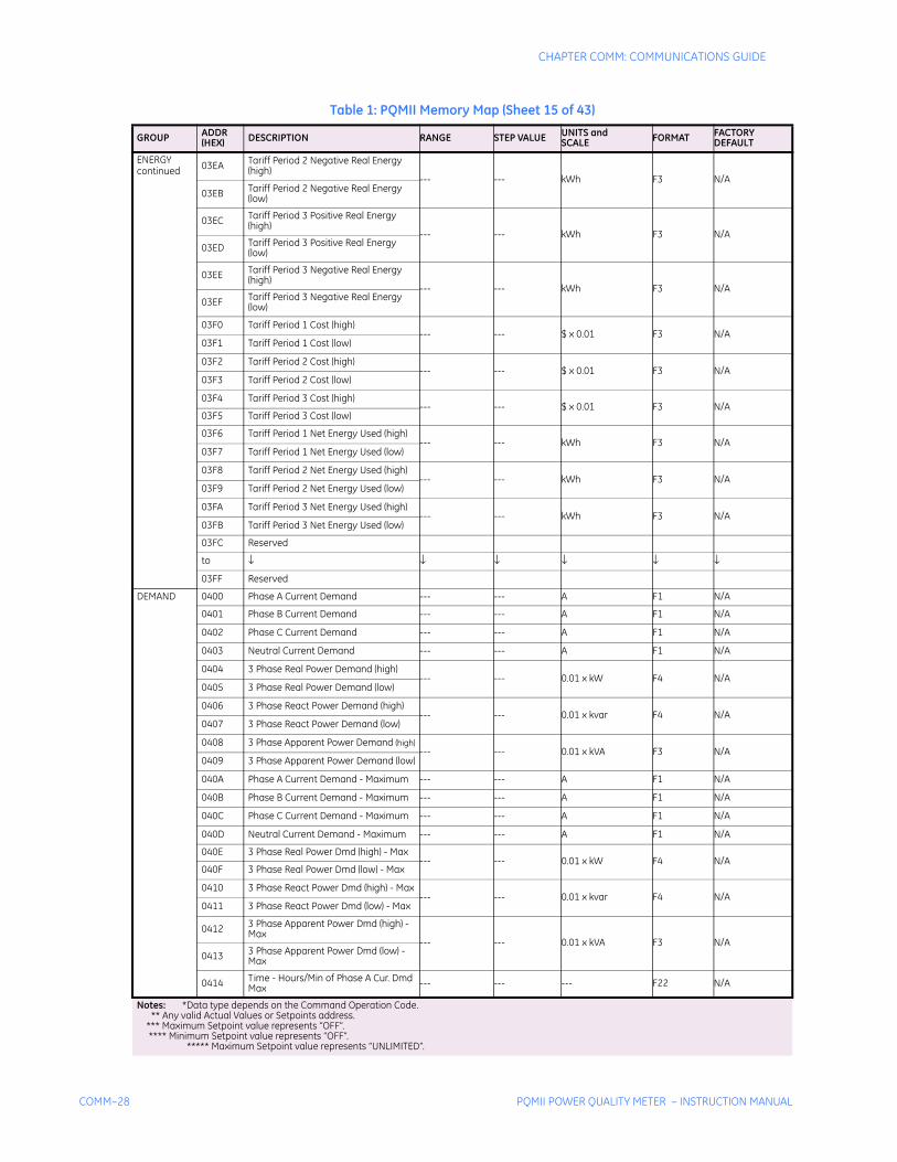
COMM–28 PQMII POWER QUALITY METER – INSTRUCTION MANUAL
CHAPTER COMM: COMMUNICATIONS GUIDE
ENERGYcontinued 03EA Tariff Period 2 Negative Real Energy
(high)--- --- kWh F3 N/A
03EB Tariff Period 2 Negative Real Energy (low)
03EC Tariff Period 3 Positive Real Energy (high)
--- --- kWh F3 N/A03ED Tariff Period 3 Positive Real Energy
(low)
03EE Tariff Period 3 Negative Real Energy (high)
--- --- kWh F3 N/A03EF Tariff Period 3 Negative Real Energy
(low)
03F0 Tariff Period 1 Cost (high)--- --- $ x 0.01 F3 N/A
03F1 Tariff Period 1 Cost (low)
03F2 Tariff Period 2 Cost (high)--- --- $ x 0.01 F3 N/A
03F3 Tariff Period 2 Cost (low)
03F4 Tariff Period 3 Cost (high)--- --- $ x 0.01 F3 N/A
03F5 Tariff Period 3 Cost (low)
03F6 Tariff Period 1 Net Energy Used (high)--- --- kWh F3 N/A
03F7 Tariff Period 1 Net Energy Used (low)
03F8 Tariff Period 2 Net Energy Used (high)--- --- kWh F3 N/A
03F9 Tariff Period 2 Net Energy Used (low)
03FA Tariff Period 3 Net Energy Used (high)--- --- kWh F3 N/A
03FB Tariff Period 3 Net Energy Used (low)
03FC Reserved
to ↓ ↓ ↓ ↓ ↓ ↓
03FF Reserved
DEMAND 0400 Phase A Current Demand --- --- A F1 N/A
0401 Phase B Current Demand --- --- A F1 N/A
0402 Phase C Current Demand --- --- A F1 N/A
0403 Neutral Current Demand --- --- A F1 N/A
0404 3 Phase Real Power Demand (high)--- --- 0.01 x kW F4 N/A
0405 3 Phase Real Power Demand (low)
0406 3 Phase React Power Demand (high)--- --- 0.01 x kvar F4 N/A
0407 3 Phase React Power Demand (low)
0408 3 Phase Apparent Power Demand (high)--- --- 0.01 x kVA F3 N/A
0409 3 Phase Apparent Power Demand (low)
040A Phase A Current Demand - Maximum --- --- A F1 N/A
040B Phase B Current Demand - Maximum --- --- A F1 N/A
040C Phase C Current Demand - Maximum --- --- A F1 N/A
040D Neutral Current Demand - Maximum --- --- A F1 N/A
040E 3 Phase Real Power Dmd (high) - Max--- --- 0.01 x kW F4 N/A
040F 3 Phase Real Power Dmd (low) - Max
0410 3 Phase React Power Dmd (high) - Max--- --- 0.01 x kvar F4 N/A
0411 3 Phase React Power Dmd (low) - Max
0412 3 Phase Apparent Power Dmd (high) - Max
--- --- 0.01 x kVA F3 N/A0413 3 Phase Apparent Power Dmd (low) -
Max
0414 Time - Hours/Min of Phase A Cur. Dmd Max --- --- --- F22 N/A
Table 1: PQMII Memory Map (Sheet 15 of 43)
GROUP ADDR(HEX) DESCRIPTION RANGE STEP VALUE UNITS and
SCALE FORMAT FACTORY DEFAULT
Notes: *Data type depends on the Command Operation Code. ** Any valid Actual Values or Setpoints address. *** Maximum Setpoint value represents “OFF”. **** Minimum Setpoint value represents “OFF”. ***** Maximum Setpoint value represents “UNLIMITED”.
CHAPTER COMM: COMMUNICATIONS GUIDE
PQMII POWER QUALITY METER – INSTRUCTION MANUAL COMM–29
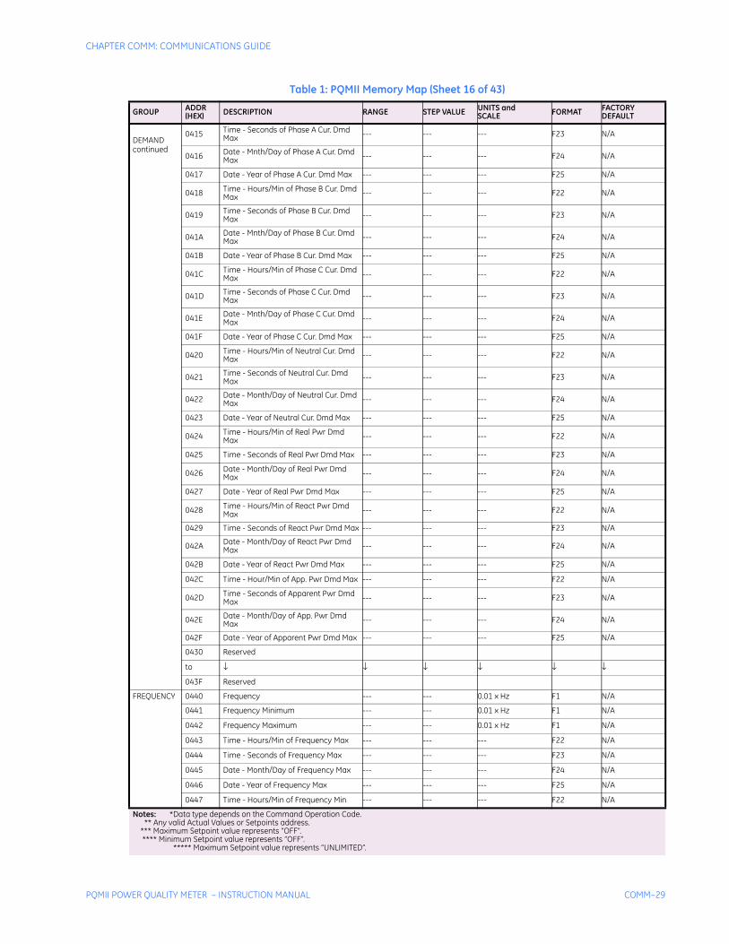
DEMANDcontinued
0415 Time - Seconds of Phase A Cur. Dmd Max --- --- --- F23 N/A
0416 Date - Mnth/Day of Phase A Cur. Dmd Max --- --- --- F24 N/A
0417 Date - Year of Phase A Cur. Dmd Max --- --- --- F25 N/A
0418 Time - Hours/Min of Phase B Cur. Dmd Max --- --- --- F22 N/A
0419 Time - Seconds of Phase B Cur. Dmd Max --- --- --- F23 N/A
041A Date - Mnth/Day of Phase B Cur. Dmd Max --- --- --- F24 N/A
041B Date - Year of Phase B Cur. Dmd Max --- --- --- F25 N/A
041C Time - Hours/Min of Phase C Cur. Dmd Max --- --- --- F22 N/A
041D Time - Seconds of Phase C Cur. Dmd Max --- --- --- F23 N/A
041E Date - Mnth/Day of Phase C Cur. Dmd Max --- --- --- F24 N/A
041F Date - Year of Phase C Cur. Dmd Max --- --- --- F25 N/A
0420 Time - Hours/Min of Neutral Cur. Dmd Max --- --- --- F22 N/A
0421 Time - Seconds of Neutral Cur. Dmd Max --- --- --- F23 N/A
0422 Date - Month/Day of Neutral Cur. Dmd Max --- --- --- F24 N/A
0423 Date - Year of Neutral Cur. Dmd Max --- --- --- F25 N/A
0424 Time - Hours/Min of Real Pwr Dmd Max --- --- --- F22 N/A
0425 Time - Seconds of Real Pwr Dmd Max --- --- --- F23 N/A
0426 Date - Month/Day of Real Pwr Dmd Max --- --- --- F24 N/A
0427 Date - Year of Real Pwr Dmd Max --- --- --- F25 N/A
0428 Time - Hours/Min of React Pwr Dmd Max --- --- --- F22 N/A
0429 Time - Seconds of React Pwr Dmd Max --- --- --- F23 N/A
042A Date - Month/Day of React Pwr Dmd Max --- --- --- F24 N/A
042B Date - Year of React Pwr Dmd Max --- --- --- F25 N/A
042C Time - Hour/Min of App. Pwr Dmd Max --- --- --- F22 N/A
042D Time - Seconds of Apparent Pwr Dmd Max --- --- --- F23 N/A
042E Date - Month/Day of App. Pwr Dmd Max --- --- --- F24 N/A
042F Date - Year of Apparent Pwr Dmd Max --- --- --- F25 N/A
0430 Reserved
to ↓ ↓ ↓ ↓ ↓ ↓
043F Reserved
FREQUENCY 0440 Frequency --- --- 0.01 x Hz F1 N/A
0441 Frequency Minimum --- --- 0.01 x Hz F1 N/A
0442 Frequency Maximum --- --- 0.01 x Hz F1 N/A
0443 Time - Hours/Min of Frequency Max --- --- --- F22 N/A
0444 Time - Seconds of Frequency Max --- --- --- F23 N/A
0445 Date - Month/Day of Frequency Max --- --- --- F24 N/A
0446 Date - Year of Frequency Max --- --- --- F25 N/A
0447 Time - Hours/Min of Frequency Min --- --- --- F22 N/A
Table 1: PQMII Memory Map (Sheet 16 of 43)
GROUP ADDR(HEX) DESCRIPTION RANGE STEP VALUE UNITS and
SCALE FORMAT FACTORY DEFAULT
Notes: *Data type depends on the Command Operation Code. ** Any valid Actual Values or Setpoints address. *** Maximum Setpoint value represents “OFF”. **** Minimum Setpoint value represents “OFF”. ***** Maximum Setpoint value represents “UNLIMITED”.
COMM–30 PQMII POWER QUALITY METER – INSTRUCTION MANUAL
CHAPTER COMM: COMMUNICATIONS GUIDE
FREQUENCYcontinued
0448 Time - Seconds of Frequency Min --- --- --- F23 N/A
0449 Date - Month/Day of Frequency Min --- --- --- F24 N/A
044A Date - Year of Frequency Min --- --- --- F25 N/A
044B Reserved
to ↓ ↓ ↓ ↓ ↓ ↓
044F Reserved
PULSE INPUTCOUNTERS
0450 Pulse Input 1 (high)--- --- --- F3 N/A
0451 Pulse Input 1 (low)
0452 Pulse Input 2 (high)--- --- --- F3 N/A
0453 Pulse Input 2 (low)
0454 Pulse Input 3 (high)--- --- --- F3 N/A
0455 Pulse Input 3 (low)
0456 Pulse Input 4 (high)--- --- --- F3 N/A
0457 Pulse Input 4 (low)
ANALOGINPUT
0458 Main/Alternate Analog Input (High)--- --- --- F3 N/A
0459 Main/Alternate Analog Input (low)
045A Reserved
to ↓ ↓ ↓ ↓ ↓ ↓
045F Reserved
PULSE INPUTCOUNTERS
0460 Totalized Pulse Input (high)--- --- --- F3 N/A
0461 Totalized Pulse Input (low)
0462 Pulse Count Cleared Time – Hours/Min --- --- --- F22 N/A
0463 Pulse Count Cleared Time – Seconds --- --- --- F23 N/A
0464 Pulse Count Cleared Date – Month/Day --- --- --- F24 N/A
0465 Pulse Count Cleared Date – Year --- --- --- F25 N/A
0466 Reserved
to ↓ ↓ ↓ ↓ ↓ ↓
046F Reserved
POWERQUALITY
0470 Ia Crest Factor --- --- 0.001 xCF F1 N/A
0471 Ib Crest Factor --- --- 0.001 xCF F1 N/A
0472 Ic Crest Factor --- --- 0.001 xCF F1 N/A
0473 Ia Transformer Harmonic Derating Factor --- --- 0.01xTHDF F1 N/A
0474 Ib Transformer Harmonic Derating Factor --- --- 0.01xTHDF F1 N/A
0475 Ic Transformer Harmonic Derating Factor --- --- 0.01xTHDF F1 N/A
0476 Reserved
0477 Reserved
TOTALHARMONICDISTORTION
0478 Phase A Current THD --- --- 0.1 x % F1 N/A
0479 Phase B Current THD --- --- 0.1 x % F1 N/A
047A Phase C Current THD --- --- 0.1 x % F1 N/A
047B Neutral Current THD --- --- 0.1 x % F1 N/A
047C Voltage Van THD --- --- 0.1 x % F1 N/A
047D Voltage Vbn THD --- --- 0.1 x % F1 N/A
047E Voltage Vcn THD --- --- 0.1 x % F1 N/A
047F Voltage Vab THD --- --- 0.1 x % F1 N/A
0480 Voltage Vbc THD --- --- 0.1 x % F1 N/A
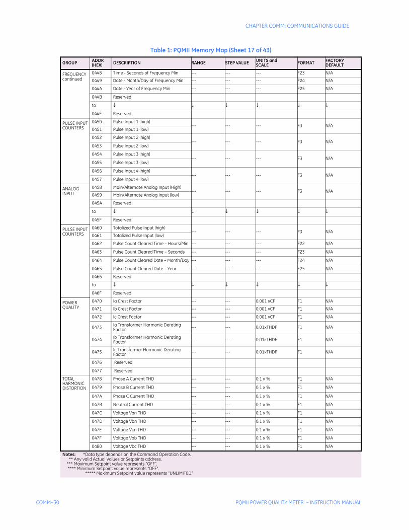
Table 1: PQMII Memory Map (Sheet 17 of 43)
GROUP ADDR(HEX) DESCRIPTION RANGE STEP VALUE UNITS and
SCALE FORMAT FACTORY DEFAULT
Notes: *Data type depends on the Command Operation Code. ** Any valid Actual Values or Setpoints address. *** Maximum Setpoint value represents “OFF”. **** Minimum Setpoint value represents “OFF”. ***** Maximum Setpoint value represents “UNLIMITED”.
CHAPTER COMM: COMMUNICATIONS GUIDE
PQMII POWER QUALITY METER – INSTRUCTION MANUAL COMM–31
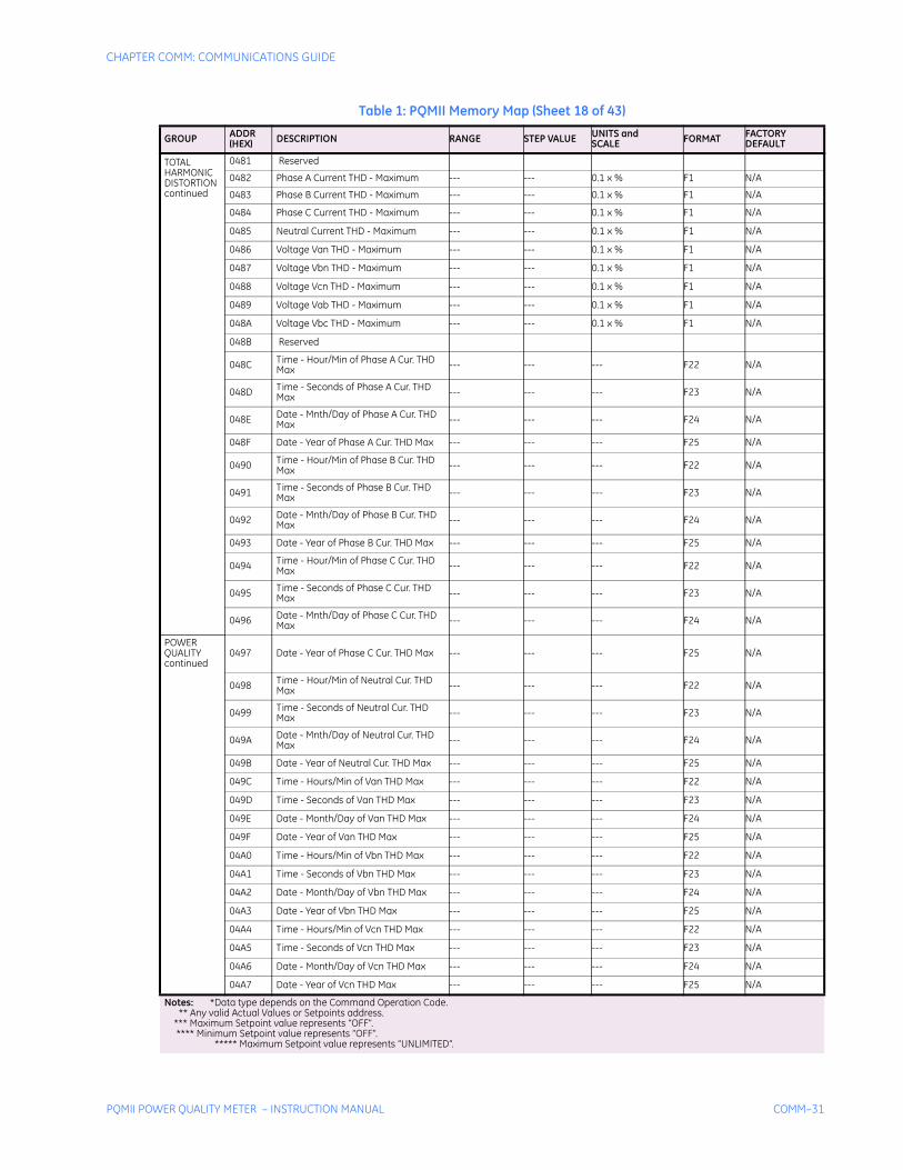
TOTALHARMONICDISTORTION continued
0481 Reserved
0482 Phase A Current THD - Maximum --- --- 0.1 x % F1 N/A
0483 Phase B Current THD - Maximum --- --- 0.1 x % F1 N/A
0484 Phase C Current THD - Maximum --- --- 0.1 x % F1 N/A
0485 Neutral Current THD - Maximum --- --- 0.1 x % F1 N/A
0486 Voltage Van THD - Maximum --- --- 0.1 x % F1 N/A
0487 Voltage Vbn THD - Maximum --- --- 0.1 x % F1 N/A
0488 Voltage Vcn THD - Maximum --- --- 0.1 x % F1 N/A
0489 Voltage Vab THD - Maximum --- --- 0.1 x % F1 N/A
048A Voltage Vbc THD - Maximum --- --- 0.1 x % F1 N/A
048B Reserved
048C Time - Hour/Min of Phase A Cur. THD Max --- --- --- F22 N/A
048D Time - Seconds of Phase A Cur. THD Max --- --- --- F23 N/A
048E Date - Mnth/Day of Phase A Cur. THD Max --- --- --- F24 N/A
048F Date - Year of Phase A Cur. THD Max --- --- --- F25 N/A
0490 Time - Hour/Min of Phase B Cur. THD Max --- --- --- F22 N/A
0491 Time - Seconds of Phase B Cur. THD Max --- --- --- F23 N/A
0492 Date - Mnth/Day of Phase B Cur. THD Max --- --- --- F24 N/A
0493 Date - Year of Phase B Cur. THD Max --- --- --- F25 N/A
0494 Time - Hour/Min of Phase C Cur. THD Max --- --- --- F22 N/A
0495 Time - Seconds of Phase C Cur. THD Max --- --- --- F23 N/A
0496 Date - Mnth/Day of Phase C Cur. THD Max --- --- --- F24 N/A
POWERQUALITYcontinued
0497 Date - Year of Phase C Cur. THD Max --- --- --- F25 N/A
0498 Time - Hour/Min of Neutral Cur. THD Max --- --- --- F22 N/A
0499 Time - Seconds of Neutral Cur. THD Max --- --- --- F23 N/A
049A Date - Mnth/Day of Neutral Cur. THD Max --- --- --- F24 N/A
049B Date - Year of Neutral Cur. THD Max --- --- --- F25 N/A
049C Time - Hours/Min of Van THD Max --- --- --- F22 N/A
049D Time - Seconds of Van THD Max --- --- --- F23 N/A
049E Date - Month/Day of Van THD Max --- --- --- F24 N/A
049F Date - Year of Van THD Max --- --- --- F25 N/A
04A0 Time - Hours/Min of Vbn THD Max --- --- --- F22 N/A
04A1 Time - Seconds of Vbn THD Max --- --- --- F23 N/A
04A2 Date - Month/Day of Vbn THD Max --- --- --- F24 N/A
04A3 Date - Year of Vbn THD Max --- --- --- F25 N/A
04A4 Time - Hours/Min of Vcn THD Max --- --- --- F22 N/A
04A5 Time - Seconds of Vcn THD Max --- --- --- F23 N/A
04A6 Date - Month/Day of Vcn THD Max --- --- --- F24 N/A
04A7 Date - Year of Vcn THD Max --- --- --- F25 N/A
Table 1: PQMII Memory Map (Sheet 18 of 43)
GROUP ADDR(HEX) DESCRIPTION RANGE STEP VALUE UNITS and
SCALE FORMAT FACTORY DEFAULT
Notes: *Data type depends on the Command Operation Code. ** Any valid Actual Values or Setpoints address. *** Maximum Setpoint value represents “OFF”. **** Minimum Setpoint value represents “OFF”. ***** Maximum Setpoint value represents “UNLIMITED”.
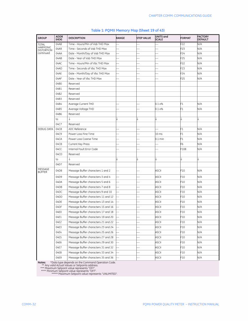
COMM–32 PQMII POWER QUALITY METER – INSTRUCTION MANUAL
CHAPTER COMM: COMMUNICATIONS GUIDE
TOTALHARMONICDISTORTIONcontinued
04A8 Time - Hours/Min of Vab THD Max --- --- --- F22 N/A
04A9 Time - Seconds of Vab THD Max --- --- --- F23 N/A
04AA Date - Month/Day of Vab THD Max --- --- --- F24 N/A
04AB Date - Year of Vab THD Max --- --- --- F25 N/A
04AC Time - Hours/Min of Vbc THD Max --- --- --- F22 N/A
04AD Time - Seconds of Vbc THD Max --- --- --- F23 N/A
04AE Date - Month/Day of Vbc THD Max --- --- --- F24 N/A
04AF Date - Year of Vbc THD Max --- --- --- F25 N/A
04B0 Reserved
04B1 Reserved
04B2 Reserved
04B3 Reserved
04B4 Average Current THD --- --- 0.1 x% F1 N/A
04B5 Average Voltage THD --- --- 0.1 x% F1 N/A
04B6 Reserved
to ↓ ↓ ↓ ↓ ↓ ↓
04C7 Reserved
DEBUG DATA 04C8 ADC Reference --- --- --- F1 N/A
04C9 Power Loss Fine Time --- --- 10 ms F1 N/A
04CA Power Loss Coarse Time --- --- 0.1 min F1 N/A
04CB Current Key Press --- --- --- F6 N/A
04CC Internal Fault Error Code --- --- --- F108 N/A
04CD Reserved
to ↓ ↓ ↓ ↓ ↓ ↓
04D7 Reserved
MESSAGEBUFFER 04D8 Message Buffer characters 1 and 2 --- --- ASCII F10 N/A
04D9 Message Buffer characters 3 and 4 --- --- ASCII F10 N/A
04DA Message Buffer characters 5 and 6 --- --- ASCII F10 N/A
04DB Message Buffer characters 7 and 8 --- --- ASCII F10 N/A
04DC Message Buffer characters 9 and 10 --- --- ASCII F10 N/A
04DD Message Buffer characters 11 and 12 --- --- ASCII F10 N/A
04DE Message Buffer characters 13 and 14 --- --- ASCII F10 N/A
04DF Message Buffer characters 15 and 16 --- --- ASCII F10 N/A
04E0 Message Buffer characters 17 and 18 --- --- ASCII F10 N/A
04E1 Message Buffer characters 19 and 20 --- --- ASCII F10 N/A
04E2 Message Buffer characters 21 and 22 --- --- ASCII F10 N/A
04E3 Message Buffer characters 23 and 24 --- --- ASCII F10 N/A
04E4 Message Buffer characters 25 and 26 --- --- ASCII F10 N/A
04E5 Message Buffer characters 27 and 28 --- --- ASCII F10 N/A
04E6 Message Buffer characters 29 and 30 --- --- ASCII F10 N/A
04E7 Message Buffer characters 31 and 32 --- --- ASCII F10 N/A
04E8 Message Buffer characters 33 and 34 --- --- ASCII F10 N/A
04E9 Message Buffer characters 35 and 36 --- --- ASCII F10 N/A
Table 1: PQMII Memory Map (Sheet 19 of 43)
GROUP ADDR(HEX) DESCRIPTION RANGE STEP VALUE UNITS and
SCALE FORMAT FACTORY DEFAULT
Notes: *Data type depends on the Command Operation Code. ** Any valid Actual Values or Setpoints address. *** Maximum Setpoint value represents “OFF”. **** Minimum Setpoint value represents “OFF”. ***** Maximum Setpoint value represents “UNLIMITED”.
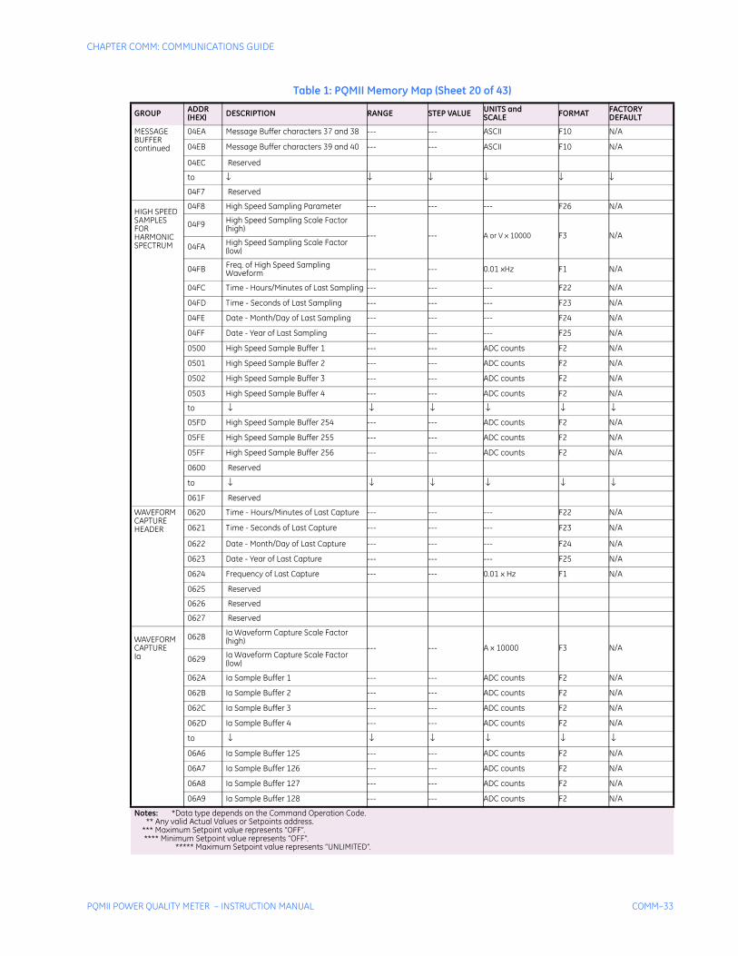
CHAPTER COMM: COMMUNICATIONS GUIDE
PQMII POWER QUALITY METER – INSTRUCTION MANUAL COMM–33
MESSAGEBUFFER continued
04EA Message Buffer characters 37 and 38 --- --- ASCII F10 N/A
04EB Message Buffer characters 39 and 40 --- --- ASCII F10 N/A
04EC Reserved
to ↓ ↓ ↓ ↓ ↓ ↓
04F7 Reserved
HIGH SPEEDSAMPLESFORHARMONICSPECTRUM
04F8 High Speed Sampling Parameter --- --- --- F26 N/A
04F9 High Speed Sampling Scale Factor (high)
--- --- A or V x 10000 F3 N/A04FA High Speed Sampling Scale Factor
(low)
04FB Freq. of High Speed Sampling Waveform --- --- 0.01 xHz F1 N/A
04FC Time - Hours/Minutes of Last Sampling --- --- --- F22 N/A
04FD Time - Seconds of Last Sampling --- --- --- F23 N/A
04FE Date - Month/Day of Last Sampling --- --- --- F24 N/A
04FF Date - Year of Last Sampling --- --- --- F25 N/A
0500 High Speed Sample Buffer 1 --- --- ADC counts F2 N/A
0501 High Speed Sample Buffer 2 --- --- ADC counts F2 N/A
0502 High Speed Sample Buffer 3 --- --- ADC counts F2 N/A
0503 High Speed Sample Buffer 4 --- --- ADC counts F2 N/A
to ↓ ↓ ↓ ↓ ↓ ↓
05FD High Speed Sample Buffer 254 --- --- ADC counts F2 N/A
05FE High Speed Sample Buffer 255 --- --- ADC counts F2 N/A
05FF High Speed Sample Buffer 256 --- --- ADC counts F2 N/A
0600 Reserved
to ↓ ↓ ↓ ↓ ↓ ↓
061F Reserved
WAVEFORMCAPTUREHEADER
0620 Time - Hours/Minutes of Last Capture --- --- --- F22 N/A
0621 Time - Seconds of Last Capture --- --- --- F23 N/A
0622 Date - Month/Day of Last Capture --- --- --- F24 N/A
0623 Date - Year of Last Capture --- --- --- F25 N/A
0624 Frequency of Last Capture --- --- 0.01 x Hz F1 N/A
0625 Reserved
0626 Reserved
0627 Reserved
WAVEFORMCAPTUREIa
0628 Ia Waveform Capture Scale Factor (high)
--- --- A x 10000 F3 N/A0629 Ia Waveform Capture Scale Factor
(low)
062A Ia Sample Buffer 1 --- --- ADC counts F2 N/A
062B Ia Sample Buffer 2 --- --- ADC counts F2 N/A
062C Ia Sample Buffer 3 --- --- ADC counts F2 N/A
062D Ia Sample Buffer 4 --- --- ADC counts F2 N/A
to ↓ ↓ ↓ ↓ ↓ ↓
06A6 Ia Sample Buffer 125 --- --- ADC counts F2 N/A
06A7 Ia Sample Buffer 126 --- --- ADC counts F2 N/A
06A8 Ia Sample Buffer 127 --- --- ADC counts F2 N/A
06A9 Ia Sample Buffer 128 --- --- ADC counts F2 N/A
Table 1: PQMII Memory Map (Sheet 20 of 43)
GROUP ADDR(HEX) DESCRIPTION RANGE STEP VALUE UNITS and
SCALE FORMAT FACTORY DEFAULT
Notes: *Data type depends on the Command Operation Code. ** Any valid Actual Values or Setpoints address. *** Maximum Setpoint value represents “OFF”. **** Minimum Setpoint value represents “OFF”. ***** Maximum Setpoint value represents “UNLIMITED”.
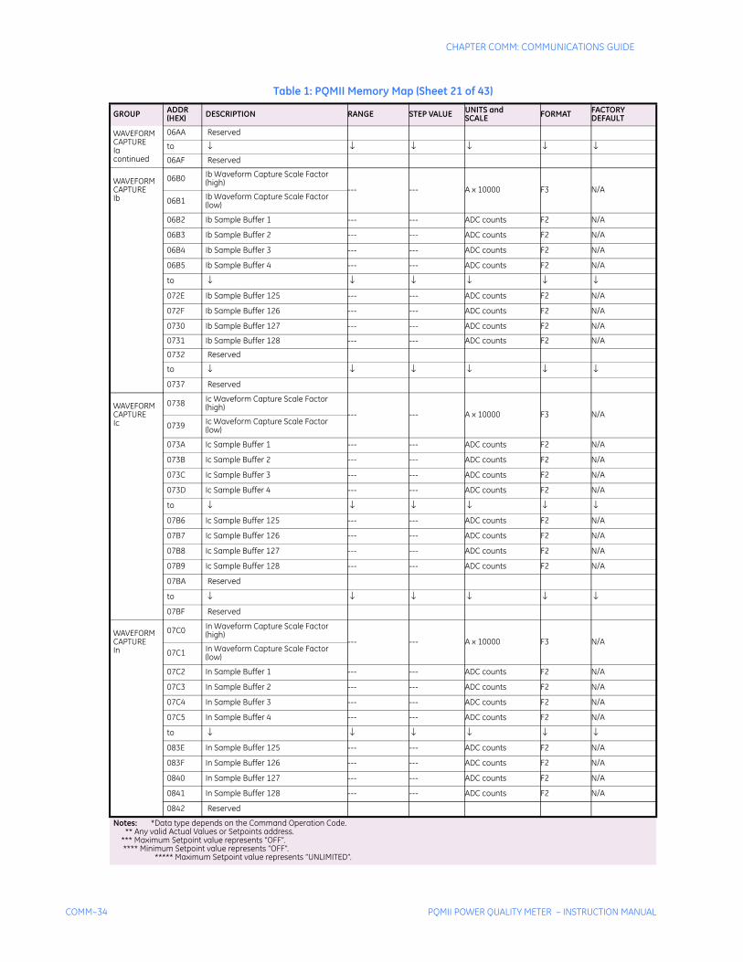
COMM–34 PQMII POWER QUALITY METER – INSTRUCTION MANUAL
CHAPTER COMM: COMMUNICATIONS GUIDE
WAVEFORMCAPTUREIacontinued
06AA Reserved
to ↓ ↓ ↓ ↓ ↓ ↓
06AF Reserved
WAVEFORMCAPTUREIb
06B0 Ib Waveform Capture Scale Factor (high)
--- --- A x 10000 F3 N/A06B1 Ib Waveform Capture Scale Factor
(low)
06B2 Ib Sample Buffer 1 --- --- ADC counts F2 N/A
06B3 Ib Sample Buffer 2 --- --- ADC counts F2 N/A
06B4 Ib Sample Buffer 3 --- --- ADC counts F2 N/A
06B5 Ib Sample Buffer 4 --- --- ADC counts F2 N/A
to ↓ ↓ ↓ ↓ ↓ ↓
072E Ib Sample Buffer 125 --- --- ADC counts F2 N/A
072F Ib Sample Buffer 126 --- --- ADC counts F2 N/A
0730 Ib Sample Buffer 127 --- --- ADC counts F2 N/A
0731 Ib Sample Buffer 128 --- --- ADC counts F2 N/A
0732 Reserved
to ↓ ↓ ↓ ↓ ↓ ↓
0737 Reserved
WAVEFORMCAPTUREIc
0738 Ic Waveform Capture Scale Factor (high)
--- --- A x 10000 F3 N/A0739 Ic Waveform Capture Scale Factor
(low)
073A Ic Sample Buffer 1 --- --- ADC counts F2 N/A
073B Ic Sample Buffer 2 --- --- ADC counts F2 N/A
073C Ic Sample Buffer 3 --- --- ADC counts F2 N/A
073D Ic Sample Buffer 4 --- --- ADC counts F2 N/A
to ↓ ↓ ↓ ↓ ↓ ↓
07B6 Ic Sample Buffer 125 --- --- ADC counts F2 N/A
07B7 Ic Sample Buffer 126 --- --- ADC counts F2 N/A
07B8 Ic Sample Buffer 127 --- --- ADC counts F2 N/A
07B9 Ic Sample Buffer 128 --- --- ADC counts F2 N/A
07BA Reserved
to ↓ ↓ ↓ ↓ ↓ ↓
07BF Reserved
WAVEFORMCAPTUREIn
07C0 In Waveform Capture Scale Factor (high)
--- --- A x 10000 F3 N/A07C1 In Waveform Capture Scale Factor
(low)
07C2 In Sample Buffer 1 --- --- ADC counts F2 N/A
07C3 In Sample Buffer 2 --- --- ADC counts F2 N/A
07C4 In Sample Buffer 3 --- --- ADC counts F2 N/A
07C5 In Sample Buffer 4 --- --- ADC counts F2 N/A
to ↓ ↓ ↓ ↓ ↓ ↓
083E In Sample Buffer 125 --- --- ADC counts F2 N/A
083F In Sample Buffer 126 --- --- ADC counts F2 N/A
0840 In Sample Buffer 127 --- --- ADC counts F2 N/A
0841 In Sample Buffer 128 --- --- ADC counts F2 N/A
0842 Reserved
Table 1: PQMII Memory Map (Sheet 21 of 43)
GROUP ADDR(HEX) DESCRIPTION RANGE STEP VALUE UNITS and
SCALE FORMAT FACTORY DEFAULT
Notes: *Data type depends on the Command Operation Code. ** Any valid Actual Values or Setpoints address. *** Maximum Setpoint value represents “OFF”. **** Minimum Setpoint value represents “OFF”. ***** Maximum Setpoint value represents “UNLIMITED”.
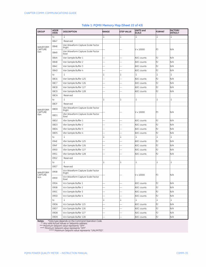
CHAPTER COMM: COMMUNICATIONS GUIDE
PQMII POWER QUALITY METER – INSTRUCTION MANUAL COMM–35
to ↓ ↓ ↓ ↓ ↓ ↓
0847 Reserved
WAVEFORMCAPTUREVan
0848 Van Waveform Capture Scale Factor (high)
--- --- V x 10000 F3 N/A0849 Van Waveform Capture Scale Factor
(low)
084A Van Sample Buffer 1 --- --- ADC counts F2 N/A
084B Van Sample Buffer 2 --- --- ADC counts F2 N/A
084C Van Sample Buffer 3 --- --- ADC counts F2 N/A
084D Van Sample Buffer 4 --- --- ADC counts F2 N/A
to ↓ ↓ ↓ ↓ ↓ ↓
08C6 Van Sample Buffer 125 --- --- ADC counts F2 N/A
08C7 Van Sample Buffer 126 --- --- ADC counts F2 N/A
08C8 Van Sample Buffer 127 --- --- ADC counts F2 N/A
08C9 Van Sample Buffer 128 --- --- ADC counts F2 N/A
08CA Reserved
to ↓ ↓ ↓ ↓ ↓ ↓
08CF Reserved
WAVEFORMCAPTUREVbn
08D0 Vbn Waveform Capture Scale Factor (high)
--- --- V x 10000 F3 N/A08D1 Vbn Waveform Capture Scale Factor
(low)
08D2 Vbn Sample Buffer 1 --- --- ADC counts F2 N/A
08D3 Vbn Sample Buffer 2 --- --- ADC counts F2 N/A
08D4 Vbn Sample Buffer 3 --- --- ADC counts F2 N/A
08D5 Vbn Sample Buffer 4 --- --- ADC counts F2 N/A
to ↓ ↓ ↓ ↓ ↓ ↓
094E Vbn Sample Buffer 125 --- --- ADC counts F2 N/A
094F Vbn Sample Buffer 126 --- --- ADC counts F2 N/A
0950 Vbn Sample Buffer 127 --- --- ADC counts F2 N/A
0951 Vbn Sample Buffer 128 --- --- ADC counts F2 N/A
0952 Reserved
to ↓ ↓ ↓ ↓ ↓ ↓
0957 Reserved
WAVEFORMCAPTUREVcn
0958 Vcn Waveform Capture Scale Factor (high)
--- --- V x 10000 F3 N/A0959 Vcn Waveform Capture Scale Factor
(low)
095A Vcn Sample Buffer 1 --- --- ADC counts F2 N/A
095B Vcn Sample Buffer 2 --- --- ADC counts F2 N/A
095C Vcn Sample Buffer 3 --- --- ADC counts F2 N/A
095D Vcn Sample Buffer 4 --- --- ADC counts F2 N/A
to ↓ ↓ ↓ ↓ ↓ ↓
09D6 Vcn Sample Buffer 125 --- --- ADC counts F2 N/A
09D7 Vcn Sample Buffer 126 --- --- ADC counts F2 N/A
09D8 Vcn Sample Buffer 127 --- --- ADC counts F2 N/A
09D9 Vcn Sample Buffer 128 --- --- ADC counts F2 N/A
Table 1: PQMII Memory Map (Sheet 22 of 43)
GROUP ADDR(HEX) DESCRIPTION RANGE STEP VALUE UNITS and
SCALE FORMAT FACTORY DEFAULT
Notes: *Data type depends on the Command Operation Code. ** Any valid Actual Values or Setpoints address. *** Maximum Setpoint value represents “OFF”. **** Minimum Setpoint value represents “OFF”. ***** Maximum Setpoint value represents “UNLIMITED”.
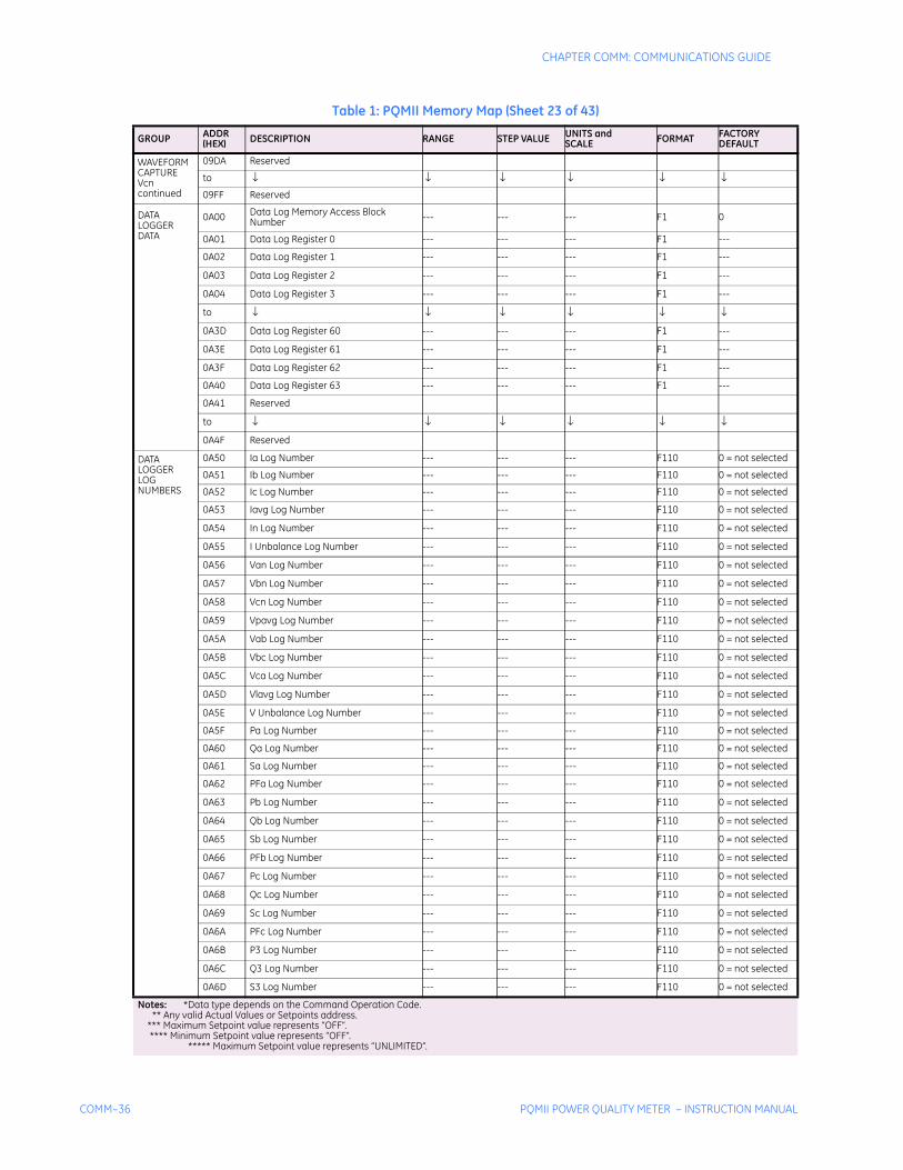
COMM–36 PQMII POWER QUALITY METER – INSTRUCTION MANUAL
CHAPTER COMM: COMMUNICATIONS GUIDE
WAVEFORMCAPTUREVcn continued
09DA Reserved
to ↓ ↓ ↓ ↓ ↓ ↓
09FF Reserved
DATALOGGERDATA
0A00 Data Log Memory Access Block Number --- --- --- F1 0
0A01 Data Log Register 0 --- --- --- F1 ---
0A02 Data Log Register 1 --- --- --- F1 ---
0A03 Data Log Register 2 --- --- --- F1 ---
0A04 Data Log Register 3 --- --- --- F1 ---
to ↓ ↓ ↓ ↓ ↓ ↓
0A3D Data Log Register 60 --- --- --- F1 ---
0A3E Data Log Register 61 --- --- --- F1 ---
0A3F Data Log Register 62 --- --- --- F1 ---
0A40 Data Log Register 63 --- --- --- F1 ---
0A41 Reserved
to ↓ ↓ ↓ ↓ ↓ ↓
0A4F Reserved
DATALOGGERLOGNUMBERS
0A50 Ia Log Number --- --- --- F110 0 = not selected
0A51 Ib Log Number --- --- --- F110 0 = not selected
0A52 Ic Log Number --- --- --- F110 0 = not selected
0A53 Iavg Log Number --- --- --- F110 0 = not selected
0A54 In Log Number --- --- --- F110 0 = not selected
0A55 I Unbalance Log Number --- --- --- F110 0 = not selected
0A56 Van Log Number --- --- --- F110 0 = not selected
0A57 Vbn Log Number --- --- --- F110 0 = not selected
0A58 Vcn Log Number --- --- --- F110 0 = not selected
0A59 Vpavg Log Number --- --- --- F110 0 = not selected
0A5A Vab Log Number --- --- --- F110 0 = not selected
0A5B Vbc Log Number --- --- --- F110 0 = not selected
0A5C Vca Log Number --- --- --- F110 0 = not selected
0A5D Vlavg Log Number --- --- --- F110 0 = not selected
0A5E V Unbalance Log Number --- --- --- F110 0 = not selected
0A5F Pa Log Number --- --- --- F110 0 = not selected
0A60 Qa Log Number --- --- --- F110 0 = not selected
0A61 Sa Log Number --- --- --- F110 0 = not selected
0A62 PFa Log Number --- --- --- F110 0 = not selected
0A63 Pb Log Number --- --- --- F110 0 = not selected
0A64 Qb Log Number --- --- --- F110 0 = not selected
0A65 Sb Log Number --- --- --- F110 0 = not selected
0A66 PFb Log Number --- --- --- F110 0 = not selected
0A67 Pc Log Number --- --- --- F110 0 = not selected
0A68 Qc Log Number --- --- --- F110 0 = not selected
0A69 Sc Log Number --- --- --- F110 0 = not selected
0A6A PFc Log Number --- --- --- F110 0 = not selected
0A6B P3 Log Number --- --- --- F110 0 = not selected
0A6C Q3 Log Number --- --- --- F110 0 = not selected
0A6D S3 Log Number --- --- --- F110 0 = not selected
Table 1: PQMII Memory Map (Sheet 23 of 43)
GROUP ADDR(HEX) DESCRIPTION RANGE STEP VALUE UNITS and
SCALE FORMAT FACTORY DEFAULT
Notes: *Data type depends on the Command Operation Code. ** Any valid Actual Values or Setpoints address. *** Maximum Setpoint value represents “OFF”. **** Minimum Setpoint value represents “OFF”. ***** Maximum Setpoint value represents “UNLIMITED”.
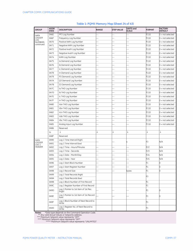
CHAPTER COMM: COMMUNICATIONS GUIDE
PQMII POWER QUALITY METER – INSTRUCTION MANUAL COMM–37
DATALOGGERLOGNUMBERScontinued
0A6E PF3 Log Number --- --- --- F110 0 = not selected
0A6F Frequency Log Number --- --- --- F110 0 = not selected
0A70 Positive kWh Log Number --- --- --- F110 0 = not selected
0A71 Negative kWh Log Number --- --- --- F110 0 = not selected
0A72 Positive kvarh Log Number --- --- --- F110 0 = not selected
0A73 Negative kvarh Log Number --- --- --- F110 0 = not selected
0A74 kVAh Log Number --- --- --- F110 0 = not selected
0A75 Ia Demand Log Number --- --- --- F110 0 = not selected
0A76 Ib Demand Log Number --- --- --- F110 0 = not selected
0A77 Ic Demand Log Number --- --- --- F110 0 = not selected
0A78 In Demand Log Number --- --- --- F110 0 = not selected
0A79 P3 Demand Log Number --- --- --- F110 0 = not selected
0A7A Q3 Demand Log Number --- --- --- F110 0 = not selected
0A7B S3 Demand Log Number --- --- --- F110 0 = not selected
0A7C Ia THD Log Number --- --- --- F110 0 = not selected
0A7D Ib THD Log Number --- --- --- F110 0 = not selected
0A7E Ic THD Log Number --- --- --- F110 0 = not selected
0A7F In THD Log Number --- --- --- F110 0 = not selected
0A80 Van THD Log Number --- --- --- F110 0 = not selected
0A81 Vbn THD Log Number --- --- --- F110 0 = not selected
0A82 Vcn THD Log Number --- --- --- F110 0 = not selected
0A83 Vab THD Log Number --- --- --- F110 0 = not selected
0A84 Vbc THD Log Number --- --- --- F110 0 = not selected
0A85 Analog Input Log Number --- --- --- F110 0 = not selected
0A86 Reserved
to ↓ ↓ ↓ ↓ ↓ ↓
0A8F Reserved
DATALOGGERLOG 1HEADER
0A90 Log 1 Time Interval (high)--- --- s F3 N/A
0A91 Log 1 Time Interval (low)
0A92 Log 1 Time - Hours/Minutes --- --- --- F22 N/A
0A93 Log 1 Time - Seconds --- --- --- F23 N/A
0A94 Log 1 Date - Month/Day --- --- --- F24 N/A
0A95 Log 1 Date - Year --- --- --- F25 N/A
0A96 Log 1 Start Block Number --- --- --- F1 0
0A97 Log 1 Start Register Number --- --- --- F1 0
0A98 Log 1 Record Size --- --- bytes F1 0
0A99 Log 1 Total Records (high)F3
0A9A Log 1 Total Records (low)
0A9B Log 1 Block Number of First Record F1
0A9C Log 1 Register Number of First Record F1
0A9D Log 1 Pointer to 1st Item of 1st Rec. (high) --- --- --- F1 0
0A9E Log 1 Pointer to 1st Item of 1st Record (low) --- --- --- F1 0
0A9F Log 1 Block Number of Next Record to Write F1
0AA0 Log 1 Register No. of Next Record to Write F1
Table 1: PQMII Memory Map (Sheet 24 of 43)
GROUP ADDR(HEX) DESCRIPTION RANGE STEP VALUE UNITS and
SCALE FORMAT FACTORY DEFAULT
Notes: *Data type depends on the Command Operation Code. ** Any valid Actual Values or Setpoints address. *** Maximum Setpoint value represents “OFF”. **** Minimum Setpoint value represents “OFF”. ***** Maximum Setpoint value represents “UNLIMITED”.
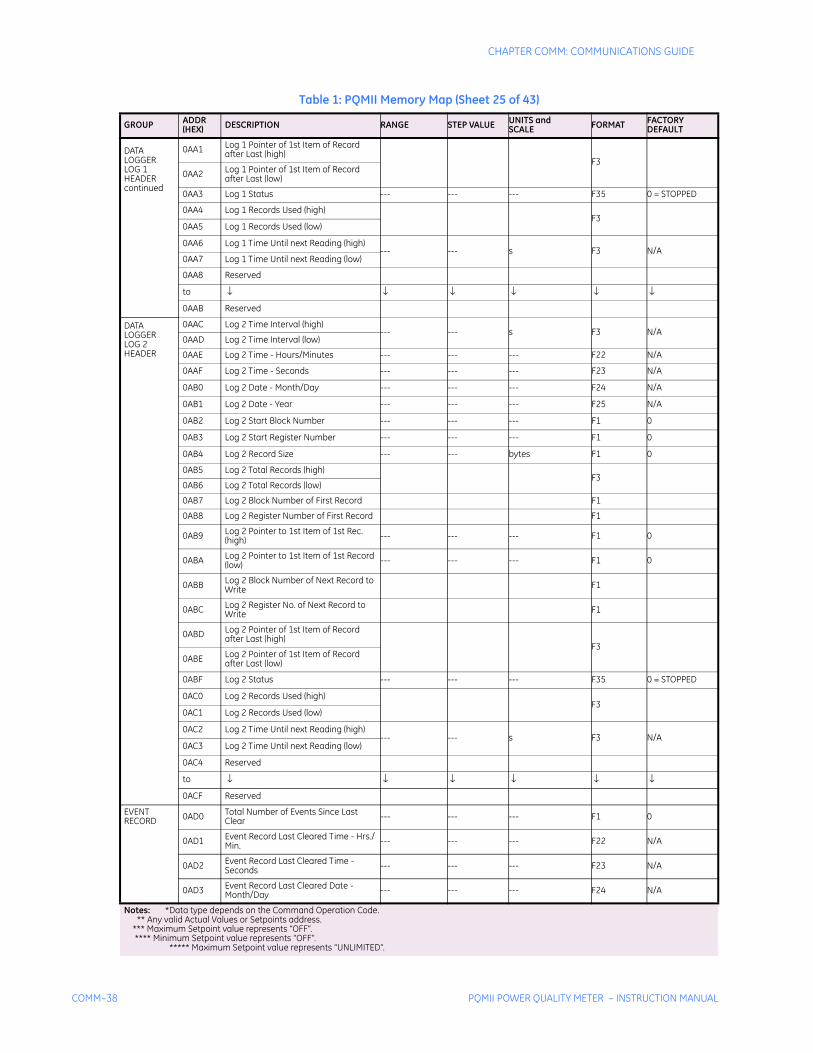
COMM–38 PQMII POWER QUALITY METER – INSTRUCTION MANUAL
CHAPTER COMM: COMMUNICATIONS GUIDE
DATALOGGERLOG 1HEADERcontinued
0AA1 Log 1 Pointer of 1st Item of Record after Last (high)
F30AA2 Log 1 Pointer of 1st Item of Record
after Last (low)
0AA3 Log 1 Status --- --- --- F35 0 = STOPPED
0AA4 Log 1 Records Used (high)F3
0AA5 Log 1 Records Used (low)
0AA6 Log 1 Time Until next Reading (high)--- --- s F3 N/A
0AA7 Log 1 Time Until next Reading (low)
0AA8 Reserved
to ↓ ↓ ↓ ↓ ↓ ↓
0AAB Reserved
DATALOGGERLOG 2HEADER
0AAC Log 2 Time Interval (high)--- --- s F3 N/A
0AAD Log 2 Time Interval (low)
0AAE Log 2 Time - Hours/Minutes --- --- --- F22 N/A
0AAF Log 2 Time - Seconds --- --- --- F23 N/A
0AB0 Log 2 Date - Month/Day --- --- --- F24 N/A
0AB1 Log 2 Date - Year --- --- --- F25 N/A
0AB2 Log 2 Start Block Number --- --- --- F1 0
0AB3 Log 2 Start Register Number --- --- --- F1 0
0AB4 Log 2 Record Size --- --- bytes F1 0
0AB5 Log 2 Total Records (high)F3
0AB6 Log 2 Total Records (low)
0AB7 Log 2 Block Number of First Record F1
0AB8 Log 2 Register Number of First Record F1
0AB9 Log 2 Pointer to 1st Item of 1st Rec. (high) --- --- --- F1 0
0ABA Log 2 Pointer to 1st Item of 1st Record (low) --- --- --- F1 0
0ABB Log 2 Block Number of Next Record to Write F1
0ABC Log 2 Register No. of Next Record to Write F1
0ABD Log 2 Pointer of 1st Item of Record after Last (high)
F30ABE Log 2 Pointer of 1st Item of Record
after Last (low)
0ABF Log 2 Status --- --- --- F35 0 = STOPPED
0AC0 Log 2 Records Used (high)F3
0AC1 Log 2 Records Used (low)
0AC2 Log 2 Time Until next Reading (high)--- --- s F3 N/A
0AC3 Log 2 Time Until next Reading (low)
0AC4 Reserved
to ↓ ↓ ↓ ↓ ↓ ↓
0ACF Reserved
EVENTRECORD 0AD0 Total Number of Events Since Last
Clear --- --- --- F1 0
0AD1 Event Record Last Cleared Time - Hrs./Min. --- --- --- F22 N/A
0AD2 Event Record Last Cleared Time - Seconds --- --- --- F23 N/A
0AD3 Event Record Last Cleared Date - Month/Day --- --- --- F24 N/A
Table 1: PQMII Memory Map (Sheet 25 of 43)
GROUP ADDR(HEX) DESCRIPTION RANGE STEP VALUE UNITS and
SCALE FORMAT FACTORY DEFAULT
Notes: *Data type depends on the Command Operation Code. ** Any valid Actual Values or Setpoints address. *** Maximum Setpoint value represents “OFF”. **** Minimum Setpoint value represents “OFF”. ***** Maximum Setpoint value represents “UNLIMITED”.
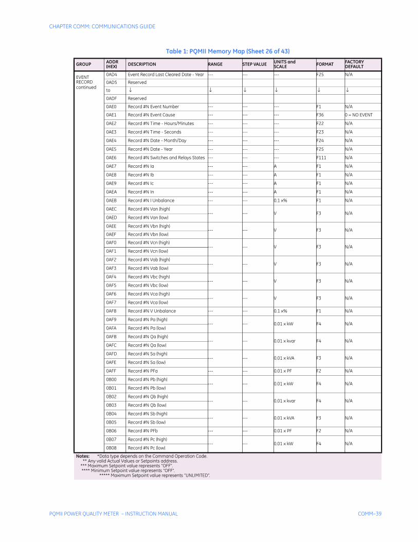
CHAPTER COMM: COMMUNICATIONS GUIDE
PQMII POWER QUALITY METER – INSTRUCTION MANUAL COMM–39
EVENTRECORDcontinued
0AD4 Event Record Last Cleared Date - Year --- --- --- F25 N/A
0AD5 Reserved
to ↓ ↓ ↓ ↓ ↓ ↓
0ADF Reserved
0AE0 Record #N Event Number --- --- --- F1 N/A
0AE1 Record #N Event Cause --- --- --- F36 0 = NO EVENT
0AE2 Record #N Time - Hours/Minutes --- --- --- F22 N/A
0AE3 Record #N Time - Seconds --- --- --- F23 N/A
0AE4 Record #N Date - Month/Day --- --- --- F24 N/A
0AE5 Record #N Date - Year --- --- --- F25 N/A
0AE6 Record #N Switches and Relays States --- --- --- F111 N/A
0AE7 Record #N Ia --- --- A F1 N/A
0AE8 Record #N Ib --- --- A F1 N/A
0AE9 Record #N Ic --- --- A F1 N/A
0AEA Record #N In --- --- A F1 N/A
0AEB Record #N I Unbalance --- --- 0.1 x% F1 N/A
0AEC Record #N Van (high)--- --- V F3 N/A
0AED Record #N Van (low)
0AEE Record #N Vbn (high)--- --- V F3 N/A
0AEF Record #N Vbn (low)
0AF0 Record #N Vcn (high)--- --- V F3 N/A
0AF1 Record #N Vcn (low)
0AF2 Record #N Vab (high)--- --- V F3 N/A
0AF3 Record #N Vab (low)
0AF4 Record #N Vbc (high)--- --- V F3 N/A
0AF5 Record #N Vbc (low)
0AF6 Record #N Vca (high)--- --- V F3 N/A
0AF7 Record #N Vca (low)
0AF8 Record #N V Unbalance --- --- 0.1 x% F1 N/A
0AF9 Record #N Pa (high)--- --- 0.01 x kW F4 N/A
0AFA Record #N Pa (low)
0AFB Record #N Qa (high)--- --- 0.01 x kvar F4 N/A
0AFC Record #N Qa (low)
0AFD Record #N Sa (high)--- --- 0.01 x kVA F3 N/A
0AFE Record #N Sa (low)
0AFF Record #N PFa --- --- 0.01 x PF F2 N/A
0B00 Record #N Pb (high)--- --- 0.01 x kW F4 N/A
0B01 Record #N Pb (low)
0B02 Record #N Qb (high)--- --- 0.01 x kvar F4 N/A
0B03 Record #N Qb (low)
0B04 Record #N Sb (high)--- --- 0.01 x kVA F3 N/A
0B05 Record #N Sb (low)
0B06 Record #N PFb --- --- 0.01 x PF F2 N/A
0B07 Record #N Pc (high)--- --- 0.01 x kW F4 N/A
0B08 Record #N Pc (low)
Table 1: PQMII Memory Map (Sheet 26 of 43)
GROUP ADDR(HEX) DESCRIPTION RANGE STEP VALUE UNITS and
SCALE FORMAT FACTORY DEFAULT
Notes: *Data type depends on the Command Operation Code. ** Any valid Actual Values or Setpoints address. *** Maximum Setpoint value represents “OFF”. **** Minimum Setpoint value represents “OFF”. ***** Maximum Setpoint value represents “UNLIMITED”.
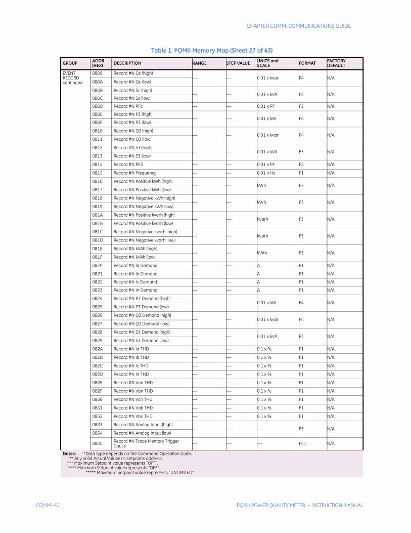
COMM–40 PQMII POWER QUALITY METER – INSTRUCTION MANUAL
CHAPTER COMM: COMMUNICATIONS GUIDE
EVENTRECORDcontinued
0B09 Record #N Qc (high)--- --- 0.01 x kvar F4 N/A
0B0A Record #N Qc (low)
0B0B Record #N Sc (high)--- --- 0.01 x kVA F3 N/A
0B0C Record #N Sc (low)
0B0D Record #N PFc --- --- 0.01 x PF F2 N/A
0B0E Record #N P3 (high)--- --- 0.01 x kW F4 N/A
0B0F Record #N P3 (low)
0B10 Record #N Q3 (high)--- --- 0.01 x kvar F4 N/A
0B11 Record #N Q3 (low)
0B12 Record #N S3 (high)--- --- 0.01 x kVA F3 N/A
0B13 Record #N S3 (low)
0B14 Record #N PF3 --- --- 0.01 x PF F2 N/A
0B15 Record #N Frequency --- --- 0.01 x Hz F1 N/A
0B16 Record #N Positive kWh (high)--- --- kWh F3 N/A
0B17 Record #N Positive kWh (low)
0B18 Record #N Negative kWh (high)--- --- kWh F3 N/A
0B19 Record #N Negative kWh (low)
0B1A Record #N Positive kvarh (high)--- --- kvarh F3 N/A
0B1B Record #N Positive kvarh (low)
0B1C Record #N Negative kvarh (high)--- --- kvarh F3 N/A
0B1D Record #N Negative kvarh (low)
0B1E Record #N kVAh (high)--- --- kVAh F3 N/A
0B1F Record #N kVAh (low)
0B20 Record #N Ia Demand --- --- A F1 N/A
0B21 Record #N Ib Demand --- --- A F1 N/A
0B22 Record #N Ic Demand --- --- A F1 N/A
0B23 Record #N In Demand --- --- A F1 N/A
0B24 Record #N P3 Demand (high)--- --- 0.01 x kW F4 N/A
0B25 Record #N P3 Demand (low)
0B26 Record #N Q3 Demand (high)--- --- 0.01 x kvar F4 N/A
0B27 Record #N Q3 Demand (low)
0B28 Record #N S3 Demand (high)--- --- 0.01 x kVA F3 N/A
0B29 Record #N S3 Demand (low)
0B2A Record #N Ia THD --- --- 0.1 x % F1 N/A
0B2B Record #N Ib THD --- --- 0.1 x % F1 N/A
0B2C Record #N Ic THD --- --- 0.1 x % F1 N/A
0B2D Record #N In THD --- --- 0.1 x % F1 N/A
0B2E Record #N Van THD --- --- 0.1 x % F1 N/A
0B2F Record #N Vbn THD --- --- 0.1 x % F1 N/A
0B30 Record #N Vcn THD --- --- 0.1 x % F1 N/A
0B31 Record #N Vab THD --- --- 0.1 x % F1 N/A
0B32 Record #N Vbc THD --- --- 0.1 x % F1 N/A
0B33 Record #N Analog Input (high)--- --- --- F3 N/A
0B34 Record #N Analog Input (low)
0B35 Record #N Trace Memory Trigger Cause --- --- --- F41 N/A
Table 1: PQMII Memory Map (Sheet 27 of 43)
GROUP ADDR(HEX) DESCRIPTION RANGE STEP VALUE UNITS and
SCALE FORMAT FACTORY DEFAULT
Notes: *Data type depends on the Command Operation Code. ** Any valid Actual Values or Setpoints address. *** Maximum Setpoint value represents “OFF”. **** Minimum Setpoint value represents “OFF”. ***** Maximum Setpoint value represents “UNLIMITED”.
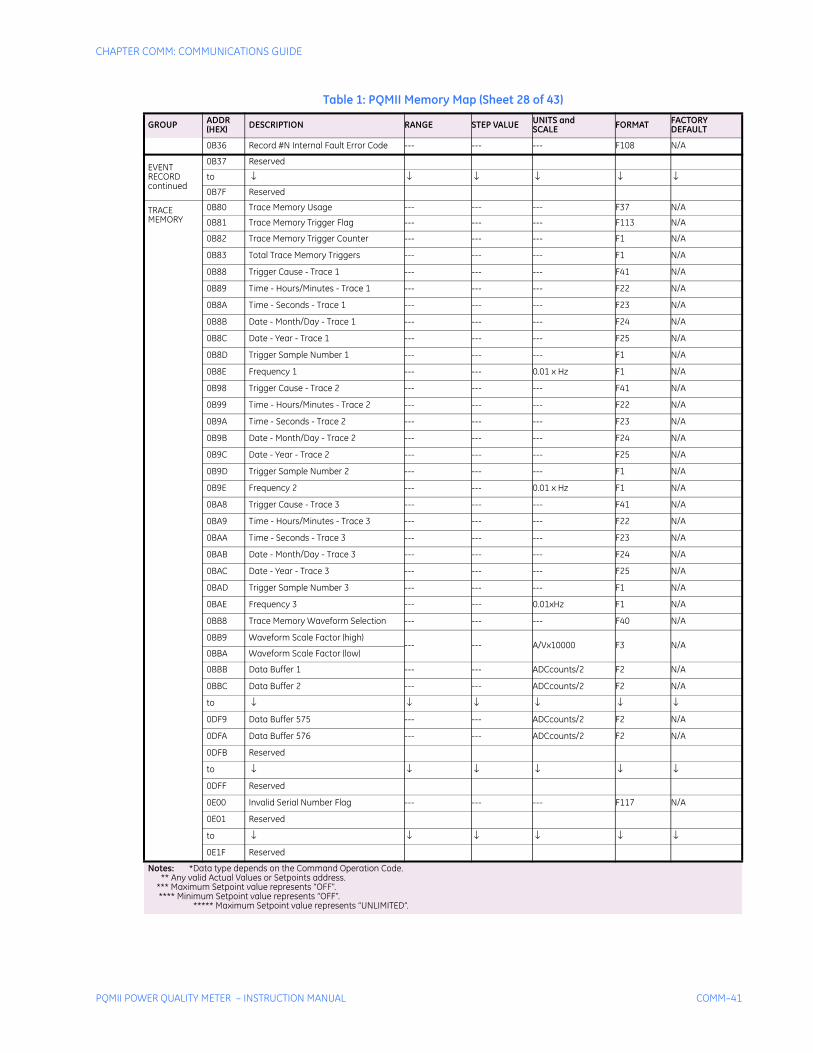
CHAPTER COMM: COMMUNICATIONS GUIDE
PQMII POWER QUALITY METER – INSTRUCTION MANUAL COMM–41
0B36 Record #N Internal Fault Error Code --- --- --- F108 N/A
EVENTRECORDcontinued
0B37 Reserved
to ↓ ↓ ↓ ↓ ↓ ↓
0B7F Reserved
TRACEMEMORY
0B80 Trace Memory Usage --- --- --- F37 N/A
0B81 Trace Memory Trigger Flag --- --- --- F113 N/A
0B82 Trace Memory Trigger Counter --- --- --- F1 N/A
0B83 Total Trace Memory Triggers --- --- --- F1 N/A
0B88 Trigger Cause - Trace 1 --- --- --- F41 N/A
0B89 Time - Hours/Minutes - Trace 1 --- --- --- F22 N/A
0B8A Time - Seconds - Trace 1 --- --- --- F23 N/A
0B8B Date - Month/Day - Trace 1 --- --- --- F24 N/A
0B8C Date - Year - Trace 1 --- --- --- F25 N/A
0B8D Trigger Sample Number 1 --- --- --- F1 N/A
0B8E Frequency 1 --- --- 0.01 x Hz F1 N/A
0B98 Trigger Cause - Trace 2 --- --- --- F41 N/A
0B99 Time - Hours/Minutes - Trace 2 --- --- --- F22 N/A
0B9A Time - Seconds - Trace 2 --- --- --- F23 N/A
0B9B Date - Month/Day - Trace 2 --- --- --- F24 N/A
0B9C Date - Year - Trace 2 --- --- --- F25 N/A
0B9D Trigger Sample Number 2 --- --- --- F1 N/A
0B9E Frequency 2 --- --- 0.01 x Hz F1 N/A
0BA8 Trigger Cause - Trace 3 --- --- --- F41 N/A
0BA9 Time - Hours/Minutes - Trace 3 --- --- --- F22 N/A
0BAA Time - Seconds - Trace 3 --- --- --- F23 N/A
0BAB Date - Month/Day - Trace 3 --- --- --- F24 N/A
0BAC Date - Year - Trace 3 --- --- --- F25 N/A
0BAD Trigger Sample Number 3 --- --- --- F1 N/A
0BAE Frequency 3 --- --- 0.01xHz F1 N/A
0BB8 Trace Memory Waveform Selection --- --- --- F40 N/A
0BB9 Waveform Scale Factor (high)--- --- A/Vx10000 F3 N/A
0BBA Waveform Scale Factor (low)
0BBB Data Buffer 1 --- --- ADCcounts/2 F2 N/A
0BBC Data Buffer 2 --- --- ADCcounts/2 F2 N/A
to ↓ ↓ ↓ ↓ ↓ ↓
0DF9 Data Buffer 575 --- --- ADCcounts/2 F2 N/A
0DFA Data Buffer 576 --- --- ADCcounts/2 F2 N/A
0DFB Reserved
to ↓ ↓ ↓ ↓ ↓ ↓
0DFF Reserved
0E00 Invalid Serial Number Flag --- --- --- F117 N/A
0E01 Reserved
to ↓ ↓ ↓ ↓ ↓ ↓
0E1F Reserved
Table 1: PQMII Memory Map (Sheet 28 of 43)
GROUP ADDR(HEX) DESCRIPTION RANGE STEP VALUE UNITS and
SCALE FORMAT FACTORY DEFAULT
Notes: *Data type depends on the Command Operation Code. ** Any valid Actual Values or Setpoints address. *** Maximum Setpoint value represents “OFF”. **** Minimum Setpoint value represents “OFF”. ***** Maximum Setpoint value represents “UNLIMITED”.
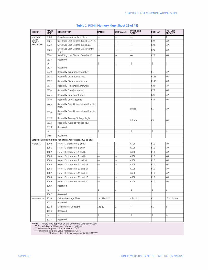
COMM–42 PQMII POWER QUALITY METER – INSTRUCTION MANUAL
CHAPTER COMM: COMMUNICATIONS GUIDE
VOLTAGE DISTUR-BANCE RECORDER
0E20 Disturbances since Last Clear --- --- --- F1 0
0E21 Swell/Sag Last Cleared Time (Hrs./Min.) --- --- --- F22 N/A
0E22 Swell/Sag Last Cleared Time (Sec.) --- --- --- F23 N/A
0E23 Swell/Sag Last Cleared Date (Month/Day.) --- --- --- F24 N/A
0E24 Swell/Sag Last Cleared Date (Year.) --- --- --- F25 N/A
0E25 Reserved
to ↓ ↓ ↓ ↓ ↓ ↓
0E2F Reserved
0E30 Record N Disturbance Number F1 N/A
0E31 Record N Disturbance Type F118 N/A
0E32 Record N Disturbance Source F119 N/A
0E33 Record N Time (hours/minutes) F22 N/A
0E34 Record N Time (seconds) F23 N/A
0E35 Record N Date (month/day) F24 N/A
0E36 Record N Date (seconds) F25 N/A
0E37 Record N Over/Undervoltage Duration (high)
cycles F3 N/A0E38 Record N Over/Undervoltage Duration
(low)
0E39 Record N Average Voltage (high)0.1 × V F3 N/A
0E3A Record N Average Voltage (low)
0E3B Reserved
to ↓ ↓ ↓ ↓ ↓ ↓
0FFF Reserved
Setpoint Values (Holding Registers) Addresses: 1000 to 131F
METER ID 1000 Meter ID characters 1 and 2 --- --- ASCII F10 N/A
1001 Meter ID characters 3 and 4 --- --- ASCII F10 N/A
1002 Meter ID characters 5 and 6 --- --- ASCII F10 N/A
1003 Meter ID characters 7 and 8 --- --- ASCII F10 N/A
1004 Meter ID characters 9 and 10 --- --- ASCII F10 N/A
1005 Meter ID characters 11 and 12 --- --- ASCII F10 N/A
1006 Meter ID characters 13 and 14 --- --- ASCII F10 N/A
1007 Meter ID characters 15 and 16 --- --- ASCII F10 N/A
1008 Meter ID characters 17 and 18 --- --- ASCII F10 N/A
1009 Meter ID characters 19 and 20 --- --- ASCII F10 N/A
100A Reserved
to ↓ ↓ ↓ ↓ ↓ ↓
100F Reserved
PREFERENCES 1010 Default Message Time 1 to 1201*** 1 min x0.1 F1 10 = 1.0 min
1011 Reserved
1012 Display Filter Constant 1 to 10 1 --- F1 4
1013 Reserved
to ↓ ↓ ↓ ↓ ↓ ↓
1017 Reserved
Table 1: PQMII Memory Map (Sheet 29 of 43)
GROUP ADDR(HEX) DESCRIPTION RANGE STEP VALUE UNITS and
SCALE FORMAT FACTORY DEFAULT
Notes: *Data type depends on the Command Operation Code. ** Any valid Actual Values or Setpoints address. *** Maximum Setpoint value represents “OFF”. **** Minimum Setpoint value represents “OFF”. ***** Maximum Setpoint value represents “UNLIMITED”.
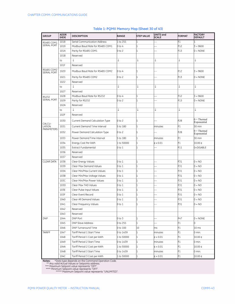
CHAPTER COMM: COMMUNICATIONS GUIDE
PQMII POWER QUALITY METER – INSTRUCTION MANUAL COMM–43
RS485 COM1SERIAL PORT
1018 Serial Communication Address 1 to 255 1 --- F1 1
1019 Modbus Baud Rate for RS485 COM1 0 to 4 1 --- F12 3 = 9600
101A Parity for RS485 COM1 0 to 2 1 --- F13 0 = NONE
101B Reserved
to ↓ ↓ ↓ ↓ ↓ ↓
101F Reserved
RS485 COM2SERIAL PORT 1020 Modbus Baud Rate for RS485 COM2 0 to 4 1 --- F12 3 = 9600
1021 Parity for RS485 COM2 0 to 2 1 --- F13 0 = NONE
1022 Reserved
to ↓ ↓ ↓ ↓ ↓ ↓
1027 Reserved
RS232SERIAL PORT
1028 Modbus Baud Rate for RS232 0 to 4 1 --- F12 3 = 9600
1029 Parity for RS232 0 to 2 1 --- F13 0 = NONE
102A Reserved
to ↓ ↓ ↓ ↓ ↓ ↓
102F Reserved
CALCU-LATIONPARAMETERS
1030 Current Demand Calculation Type 0 to 2 1 --- F28 0 = ThermalExponential
1031 Current Demand Time Interval 5 to 180 1 minutes F1 30 min
1032 Power Demand Calculation Type 0 to 2 1 --- F28 0 = ThermalExponential
1033 Power Demand Time Interval 5 to 180 1 minutes F1 30 min
1034 Energy Cost Per kWh 1 to 50000 1 ¢ x 0.01 F1 10.00 ¢
1035 Extract Fundamental 0 to 1 1 --- F11 0=DISABLE
1036 Reserved
1037 Reserved
CLEAR DATA 1038 Clear Energy Values 0 to 1 1 --- F31 0 = NO
1039 Clear Max Demand Values 0 to 1 1 --- F31 0 = NO
103A Clear Min/Max Current Values 0 to 1 1 --- F31 0 = NO
103B Clear Min/Max Voltage Values 0 to 1 1 --- F31 0 = NO
103C Clear Min/Max Power Values 0 to 1 1 --- F31 0 = NO
103D Clear Max THD Values 0 to 1 1 --- F31 0 = NO
103E Clear Pulse Input Values 0 to 1 1 --- F31 0 = NO
103F Clear Event Record 0 to 1 1 --- F31 0 = NO
1040 Clear All Demand Values 0 to 1 1 --- F31 0 = NO
1041 Clear Frequency Values 0 to 1 1 --- F31 0 = NO
1042 Reserved
1043 Reserved
DNP 1044 DNP Port 0 to 3 1 --- F47 0 = NONE
1045 DNP Slave Address 0 to 255 1 --- F1 0
1046 DNP Turnaround Time 0 to 100 10 ms F1 10 ms
TARIFF 1047 Tariff Period 1 Start Time 0 to 1439 1 minutes F1 0 min.
1048 Tariff Period 1 Cost per kWh 1 to 50000 1 ¢ × 0.01 F1 10.00 ¢
1049 Tariff Period 2 Start Time 0 to 1439 1 minutes F1 0 min.
104A Tariff Period 2 Cost per kWh 1 to 50000 1 ¢ × 0.01 F1 10.00 ¢
104B Tariff Period 3 Start Time 0 to 1439 1 minutes F1 0 min.
104C Tariff Period 3 Cost per kWh 1 to 50000 1 ¢ × 0.01 F1 10.00 ¢
Table 1: PQMII Memory Map (Sheet 30 of 43)
GROUP ADDR(HEX) DESCRIPTION RANGE STEP VALUE UNITS and
SCALE FORMAT FACTORY DEFAULT
Notes: *Data type depends on the Command Operation Code. ** Any valid Actual Values or Setpoints address. *** Maximum Setpoint value represents “OFF”. **** Minimum Setpoint value represents “OFF”. ***** Maximum Setpoint value represents “UNLIMITED”.
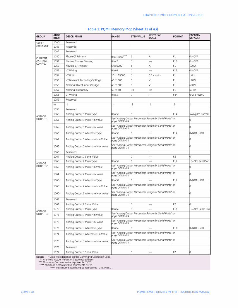
COMM–44 PQMII POWER QUALITY METER – INSTRUCTION MANUAL
CHAPTER COMM: COMMUNICATIONS GUIDE
TARIFF continued
104D Reserved
104E Reserved
104F Reserved
CURRENT/VOLTAGECONFIG.
1050 Phase CT Primary 0 to 12000**** 5 A F1 0 = OFF
1051 Neutral Current Sensing 0 to 2 1 --- F16 0 = OFF
1052 Neutral CT Primary 5 to 6000 5 A F1 100 A
1053 VT Wiring 0 to 6 1 --- F15 0 = OFF
1054 VT Ratio 10 to 35000 1 0.1 × ratio F1 1.0:1
1055 VT Nominal Secondary Voltage 40 to 600 1 V F1 120 V
1056 Nominal Direct Input Voltage 40 to 600 1 V F1 600 V
1057 Nominal Frequency 50 to 60 10 Hz F1 60 Hz
1058 CT Wiring 0 to 3 1 --- F44 0=A,B AND C
1059 Reserved
to ↓ ↓ ↓ ↓ ↓ ↓
105F Reserved
ANALOG OUTPUT 1
1060 Analog Output 1 Main Type 0 to 59 1 --- F14 5=Avg Ph Current
1061 Analog Output 1 Main Min Value See “Analog Output Parameter Range for Serial Ports” on page COMM-74 0
1062 Analog Output 1 Main Max Value See “Analog Output Parameter Range for Serial Ports” on page COMM-74 0
1063 Analog Output 1 Alternate Type 0 to 59 1 --- F14 0=NOT USED
1064 Analog Output 1 Alternate Min Value See “Analog Output Parameter Range for Serial Ports” on page COMM-74 0
1065 Analog Output 1 Alternate Max Value See “Analog Output Parameter Range for Serial Ports” on page COMM-74 0
1066 Reserved
1067 Analog Output 1 Serial Value 1 --- F2 0
ANALOG OUTPUT 2
1068 Analog Output 2 Main Type 0 to 59 1 --- F14 18=3Ph Real Pwr
1069 Analog Output 2 Main Min Value See “Analog Output Parameter Range for Serial Ports” on page COMM-74 0
106A Analog Output 2 Main Max Value See “Analog Output Parameter Range for Serial Ports” on page COMM-74 0
106B Analog Output 2 Alternate Type 0 to 59 1 --- F14 0=NOT USED
106C Analog Output 2 Alternate Min Value See “Analog Output Parameter Range for Serial Ports” on page COMM-74 0
106D Analog Output 2 Alternate Max Value See “Analog Output Parameter Range for Serial Ports” on page COMM-74 0
106E Reserved
106F Analog Output 2 Serial Value 1 --- F2 0
ANALOG OUTPUT 3
1070 Analog Output 3 Main Type 0 to 59 1 --- F14 19=3Ph React Pwr
1071 Analog Output 3 Main Min Value See “Analog Output Parameter Range for Serial Ports” on page COMM-74
1072 Analog Output 3 Main Max Value See “Analog Output Parameter Range for Serial Ports” on page COMM-74
1073 Analog Output 3 Alternate Type 0 to 59 1 --- F14 0=NOT USED
1074 Analog Output 3 Alternate Min Value See “Analog Output Parameter Range for Serial Ports” on page COMM-74
1075 Analog Output 3 Alternate Max Value See “Analog Output Parameter Range for Serial Ports” on page COMM-74
1076 Reserved
1077 Analog Output 3 Serial Value 1 --- F2 0
Table 1: PQMII Memory Map (Sheet 31 of 43)
GROUP ADDR(HEX) DESCRIPTION RANGE STEP VALUE UNITS and
SCALE FORMAT FACTORY DEFAULT
Notes: *Data type depends on the Command Operation Code. ** Any valid Actual Values or Setpoints address. *** Maximum Setpoint value represents “OFF”. **** Minimum Setpoint value represents “OFF”. ***** Maximum Setpoint value represents “UNLIMITED”.
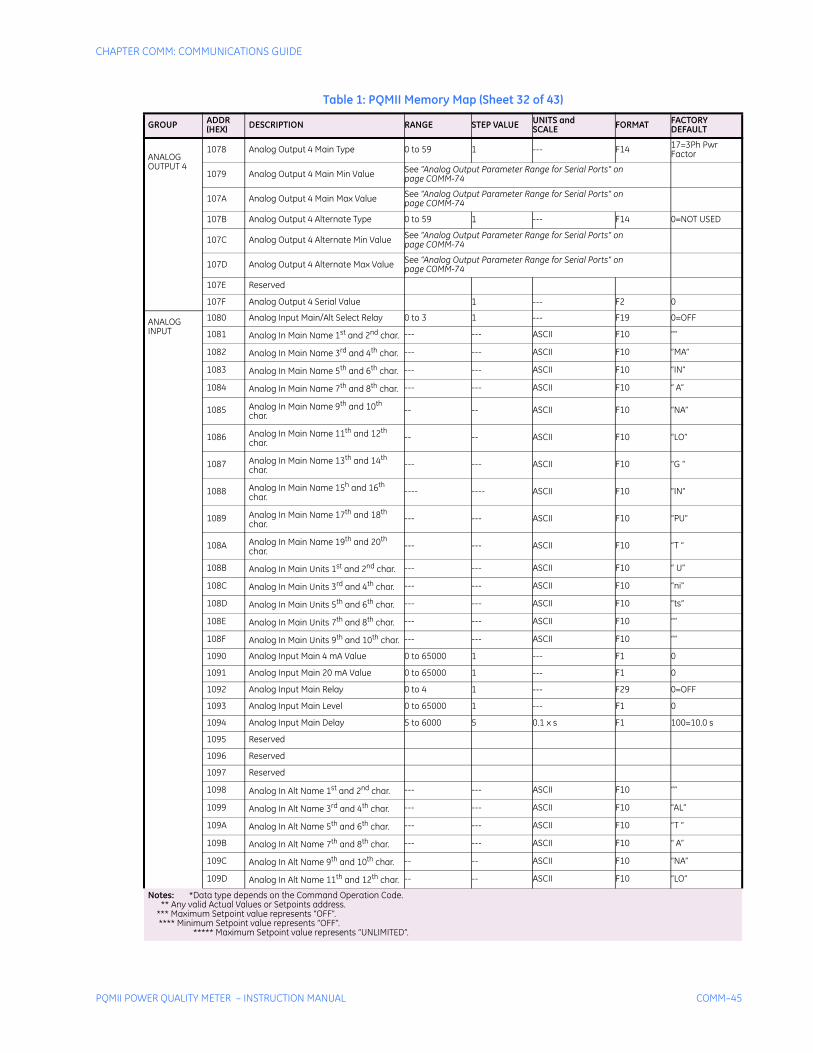
CHAPTER COMM: COMMUNICATIONS GUIDE
PQMII POWER QUALITY METER – INSTRUCTION MANUAL COMM–45
ANALOG OUTPUT 4
1078 Analog Output 4 Main Type 0 to 59 1 --- F14 17=3Ph Pwr Factor
1079 Analog Output 4 Main Min Value See “Analog Output Parameter Range for Serial Ports” on page COMM-74
107A Analog Output 4 Main Max Value See “Analog Output Parameter Range for Serial Ports” on page COMM-74
107B Analog Output 4 Alternate Type 0 to 59 1 --- F14 0=NOT USED
107C Analog Output 4 Alternate Min Value See “Analog Output Parameter Range for Serial Ports” on page COMM-74
107D Analog Output 4 Alternate Max Value See “Analog Output Parameter Range for Serial Ports” on page COMM-74
107E Reserved
107F Analog Output 4 Serial Value 1 --- F2 0
ANALOGINPUT
1080 Analog Input Main/Alt Select Relay 0 to 3 1 --- F19 0=OFF
1081 Analog In Main Name 1st and 2nd char. --- --- ASCII F10 ““
1082 Analog In Main Name 3rd and 4th char. --- --- ASCII F10 “MA”
1083 Analog In Main Name 5th and 6th char. --- --- ASCII F10 “IN”
1084 Analog In Main Name 7th and 8th char. --- --- ASCII F10 “ A”
1085 Analog In Main Name 9th and 10th char.
-- -- ASCII F10 “NA”
1086 Analog In Main Name 11th and 12th char.
-- -- ASCII F10 “LO”
1087 Analog In Main Name 13th and 14th char.
--- --- ASCII F10 “G “
1088 Analog In Main Name 15h and 16th char.
---- ---- ASCII F10 “IN”
1089 Analog In Main Name 17th and 18th char.
--- --- ASCII F10 “PU”
108A Analog In Main Name 19th and 20th char.
--- --- ASCII F10 “T “
108B Analog In Main Units 1st and 2nd char. --- --- ASCII F10 “ U”
108C Analog In Main Units 3rd and 4th char. --- --- ASCII F10 “ni”
108D Analog In Main Units 5th and 6th char. --- --- ASCII F10 “ts”
108E Analog In Main Units 7th and 8th char. --- --- ASCII F10 “”
108F Analog In Main Units 9th and 10th char. --- --- ASCII F10 ““
1090 Analog Input Main 4 mA Value 0 to 65000 1 --- F1 0
1091 Analog Input Main 20 mA Value 0 to 65000 1 --- F1 0
1092 Analog Input Main Relay 0 to 4 1 --- F29 0=OFF
1093 Analog Input Main Level 0 to 65000 1 --- F1 0
1094 Analog Input Main Delay 5 to 6000 5 0.1 x s F1 100=10.0 s
1095 Reserved
1096 Reserved
1097 Reserved
1098 Analog In Alt Name 1st and 2nd char. --- --- ASCII F10 ““
1099 Analog In Alt Name 3rd and 4th char. --- --- ASCII F10 “AL”
109A Analog In Alt Name 5th and 6th char. --- --- ASCII F10 “T ”
109B Analog In Alt Name 7th and 8th char. --- --- ASCII F10 “ A”
109C Analog In Alt Name 9th and 10th char. -- -- ASCII F10 “NA”
109D Analog In Alt Name 11th and 12th char. -- -- ASCII F10 “LO”
Table 1: PQMII Memory Map (Sheet 32 of 43)
GROUP ADDR(HEX) DESCRIPTION RANGE STEP VALUE UNITS and
SCALE FORMAT FACTORY DEFAULT
Notes: *Data type depends on the Command Operation Code. ** Any valid Actual Values or Setpoints address. *** Maximum Setpoint value represents “OFF”. **** Minimum Setpoint value represents “OFF”. ***** Maximum Setpoint value represents “UNLIMITED”.
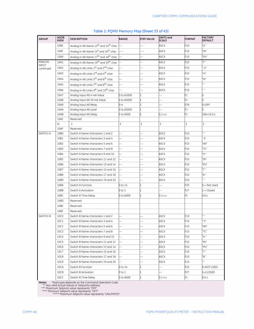
COMM–46 PQMII POWER QUALITY METER – INSTRUCTION MANUAL
CHAPTER COMM: COMMUNICATIONS GUIDE
109E Analog In Alt Name 13th and 14th char. --- --- ASCII F10 “G ”
109F Analog In Alt Name 15h and 16th char. ---- ---- ASCII F10 “IN”
10A0 Analog In Alt Name 17th and 18th char. --- --- ASCII F10 “PU”
ANALOGINPUT continued
10A1 Analog In Alt Name 19th and 20th char. --- --- ASCII F10 “T “
10A2 Analog In Alt Units 1st and 2nd char. --- --- ASCII F10 “ U”
10A3 Analog In Alt Units 3rd and 4th char. --- --- ASCII F10 “ni”
10A4 Analog In Alt Units 5th and 6th char. --- --- ASCII F10 “ts”
10A5 Analog In Alt Units 7th and 8th char. --- --- ASCII F10 “ ”
10A6 Analog In Alt Units 9th and 10th char. --- --- ASCII F10 “ ”
10A7 Analog Input Alt 4 mA Value 0 to 65000 1 --- F1 0
10A8 Analog Input Alt 20 mA Value 0 to 65000 1 --- F1 0
10A9 Analog Input Alt Relay 0-4 1 --- F29 0=OFF
10AA Analog Input Alt Level 0 to 65000 1 --- F1 0
10AB Analog Input Alt Delay 5 to 6000 5 0.1 x s F1 100=10.0 s
10AC Reserved
to ↓ ↓ ↓ ↓ ↓ ↓
10AF Reserved
SWITCH A 10B0 Switch A Name characters 1 and 2 --- --- ASCII F10 “ ”
10B1 Switch A Name characters 3 and 4 --- --- ASCII F10 “ S”
10B2 Switch A Name characters 5 and 6 --- --- ASCII F10 “WI”
10B3 Switch A Name characters 7 and 8 --- --- ASCII F10 “TC”
10B4 Switch A Name characters 9 and 10 --- --- ASCII F10 “H ”
10B5 Switch A Name characters 11 and 12 --- --- ASCII F10 “IN“
10B6 Switch A Name characters 13 and 14 --- --- ASCII F10 “PU”
10B7 Switch A Name characters 15 and 16 --- --- ASCII F10 “T ”
10B8 Switch A Name characters 17 and 18 --- --- ASCII F10 “A ”
10B9 Switch A Name characters 19 and 20 --- --- ASCII F10 “ ”
10BA Switch A Function 0 to 14 1 --- F20 0 = Not Used
10BB Switch A Activation 0 to 1 1 --- F27 1 = Closed
10BC Switch A Time Delay 0 to 6000 1 0.1 x s F1 0.0 s
10BD Reserved
10BE Reserved
10BF Reserved
SWITCH B 10C0 Switch B Name characters 1 and 2 --- --- ASCII F10 “ ”
10C1 Switch B Name characters 3 and 4 --- --- ASCII F10 “ S”
10C2 Switch B Name characters 5 and 6 --- --- ASCII F10 “WI”
10C3 Switch B Name characters 7 and 8 --- --- ASCII F10 “TC”
10C4 Switch B Name characters 9 and 10 --- --- ASCII F10 “H ”
10C5 Switch B Name characters 11 and 12 --- --- ASCII F10 “IN“
10C6 Switch B Name characters 13 and 14 --- --- ASCII F10 “PU”
10C7 Switch B Name characters 15 and 16 --- --- ASCII F10 “T ”
10C8 Switch B Name characters 17 and 18 --- --- ASCII F10 “B ”
10C9 Switch B Name characters 19 and 20 --- --- ASCII F10 “ ”
10CA Switch B Function 0 to 14 1 --- F20 0=NOT USED
10CB Switch B Activation 0 to 1 1 --- F27 1=CLOSED
10CC Switch B Time Delay 0 to 6000 1 0.1 x s F1 0.0 s
Table 1: PQMII Memory Map (Sheet 33 of 43)
GROUP ADDR(HEX) DESCRIPTION RANGE STEP VALUE UNITS and
SCALE FORMAT FACTORY DEFAULT
Notes: *Data type depends on the Command Operation Code. ** Any valid Actual Values or Setpoints address. *** Maximum Setpoint value represents “OFF”. **** Minimum Setpoint value represents “OFF”. ***** Maximum Setpoint value represents “UNLIMITED”.
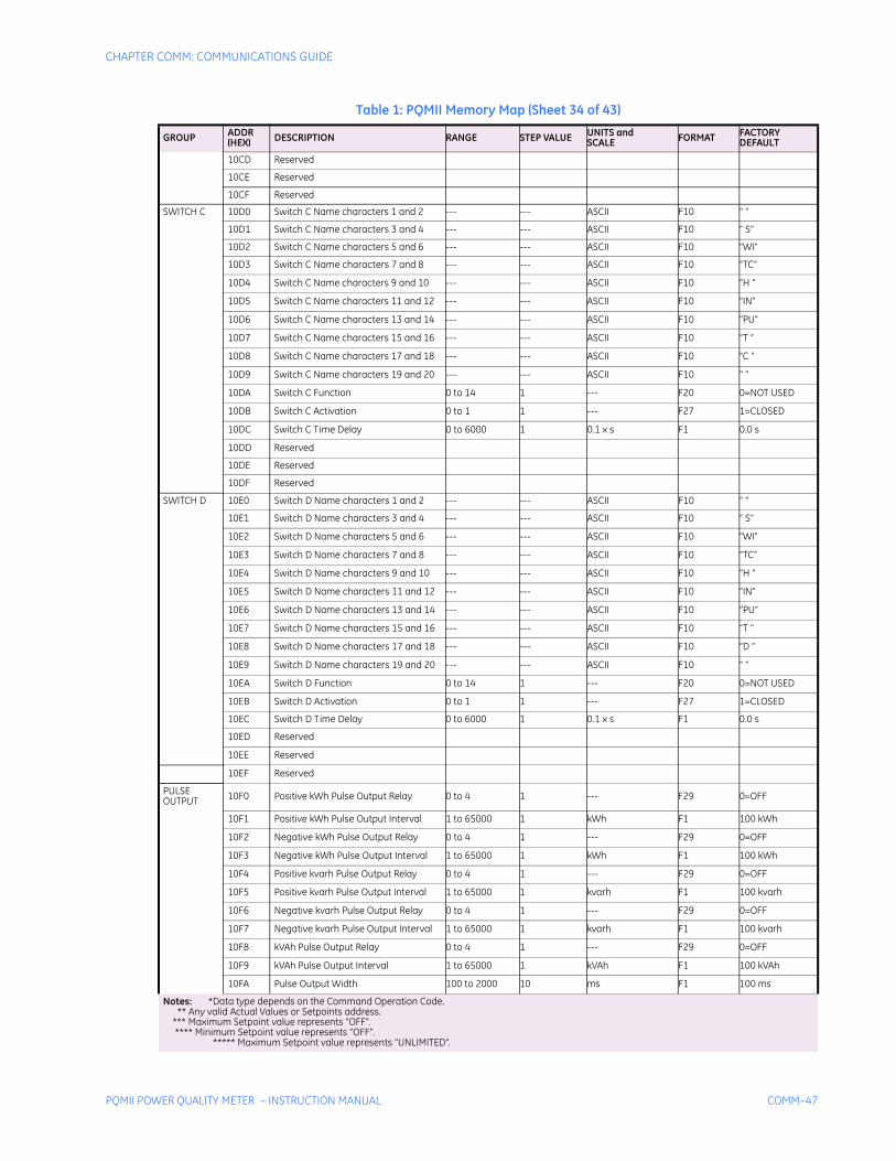
CHAPTER COMM: COMMUNICATIONS GUIDE
PQMII POWER QUALITY METER – INSTRUCTION MANUAL COMM–47
10CD Reserved
10CE Reserved
10CF Reserved
SWITCH C 10D0 Switch C Name characters 1 and 2 --- --- ASCII F10 “ ”
10D1 Switch C Name characters 3 and 4 --- --- ASCII F10 “ S”
10D2 Switch C Name characters 5 and 6 --- --- ASCII F10 “WI”
10D3 Switch C Name characters 7 and 8 --- --- ASCII F10 “TC”
10D4 Switch C Name characters 9 and 10 --- --- ASCII F10 “H ”
10D5 Switch C Name characters 11 and 12 --- --- ASCII F10 “IN”
10D6 Switch C Name characters 13 and 14 --- --- ASCII F10 “PU”
10D7 Switch C Name characters 15 and 16 --- --- ASCII F10 “T ”
10D8 Switch C Name characters 17 and 18 --- --- ASCII F10 “C ”
10D9 Switch C Name characters 19 and 20 --- --- ASCII F10 “ ”
10DA Switch C Function 0 to 14 1 --- F20 0=NOT USED
10DB Switch C Activation 0 to 1 1 --- F27 1=CLOSED
10DC Switch C Time Delay 0 to 6000 1 0.1 x s F1 0.0 s
10DD Reserved
10DE Reserved
10DF Reserved
SWITCH D 10E0 Switch D Name characters 1 and 2 --- --- ASCII F10 “ ”
10E1 Switch D Name characters 3 and 4 --- --- ASCII F10 “ S”
10E2 Switch D Name characters 5 and 6 --- --- ASCII F10 “WI”
10E3 Switch D Name characters 7 and 8 --- --- ASCII F10 “TC”
10E4 Switch D Name characters 9 and 10 --- --- ASCII F10 “H ”
10E5 Switch D Name characters 11 and 12 --- --- ASCII F10 “IN”
10E6 Switch D Name characters 13 and 14 --- --- ASCII F10 “PU”
10E7 Switch D Name characters 15 and 16 --- --- ASCII F10 “T ”
10E8 Switch D Name characters 17 and 18 --- --- ASCII F10 “D ”
10E9 Switch D Name characters 19 and 20 --- --- ASCII F10 “ ”
10EA Switch D Function 0 to 14 1 --- F20 0=NOT USED
10EB Switch D Activation 0 to 1 1 --- F27 1=CLOSED
10EC Switch D Time Delay 0 to 6000 1 0.1 x s F1 0.0 s
10ED Reserved
10EE Reserved
10EF Reserved
PULSEOUTPUT 10F0 Positive kWh Pulse Output Relay 0 to 4 1 --- F29 0=OFF
10F1 Positive kWh Pulse Output Interval 1 to 65000 1 kWh F1 100 kWh
10F2 Negative kWh Pulse Output Relay 0 to 4 1 --- F29 0=OFF
10F3 Negative kWh Pulse Output Interval 1 to 65000 1 kWh F1 100 kWh
10F4 Positive kvarh Pulse Output Relay 0 to 4 1 --- F29 0=OFF
10F5 Positive kvarh Pulse Output Interval 1 to 65000 1 kvarh F1 100 kvarh
10F6 Negative kvarh Pulse Output Relay 0 to 4 1 --- F29 0=OFF
10F7 Negative kvarh Pulse Output Interval 1 to 65000 1 kvarh F1 100 kvarh
10F8 kVAh Pulse Output Relay 0 to 4 1 --- F29 0=OFF
10F9 kVAh Pulse Output Interval 1 to 65000 1 kVAh F1 100 kVAh
10FA Pulse Output Width 100 to 2000 10 ms F1 100 ms
Table 1: PQMII Memory Map (Sheet 34 of 43)
GROUP ADDR(HEX) DESCRIPTION RANGE STEP VALUE UNITS and
SCALE FORMAT FACTORY DEFAULT
Notes: *Data type depends on the Command Operation Code. ** Any valid Actual Values or Setpoints address. *** Maximum Setpoint value represents “OFF”. **** Minimum Setpoint value represents “OFF”. ***** Maximum Setpoint value represents “UNLIMITED”.
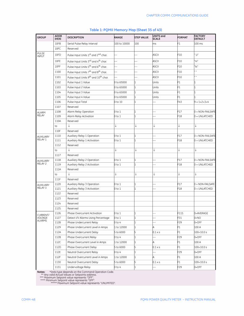
COMM–48 PQMII POWER QUALITY METER – INSTRUCTION MANUAL
CHAPTER COMM: COMMUNICATIONS GUIDE
10FB Serial Pulse Relay Interval 100 to 10000 100 ms F1 100 ms
10FC Reserved
PULSEINPUT 10FD Pulse Input Units 1st and 2nd char. --- --- ASCII F10 “ U”
10FE Pulse Input Units 3rd and 4th char. --- --- ASCII F10 “ni”
10FF Pulse Input Units 5th and 6th char. --- --- ASCII F10 “ts”
1100 Pulse Input Units 7th and 8th char. --- --- ASCII F10 “ ”
1101 Pulse Input Units 9th and 10th char. --- --- ASCII F10 “ ”
1102 Pulse Input 1 Value 0 to 65000 1 Units F1 1
1103 Pulse Input 2 Value 0 to 65000 1 Units F1 1
1104 Pulse Input 3 Value 0 to 65000 1 Units F1 1
1105 Pulse Input 4 Value 0 to 65000 1 Units F1 1
1106 Pulse Input Total 0 to 10 1 --- F43 9 = 1+2+3+4
1107 Reserved
ALARMRELAY
1108 Alarm Relay Operation 0 to 1 1 --- F17 0 = NON-FAILSAFE
1109 Alarm Relay Activation 0 to 1 1 --- F18 0 = UNLATCHED
110A Reserved
to ↓ ↓ ↓ ↓ ↓ ↓
110F Reserved
AUXILIARYRELAY 1
1110 Auxiliary Relay 1 Operation 0 to 1 1 --- F17 0 = NON-FAILSAFE
1111 Auxiliary Relay 1 Activation 0 to 1 1 --- F18 0 = UNLATCHED
1112 Reserved
to ↓ ↓ ↓ ↓ ↓ ↓
1117 Reserved
AUXILIARYRELAY 2
1118 Auxiliary Relay 2 Operation 0 to 1 1 --- F17 0 = NON-FAILSAFE
1119 Auxiliary Relay 2 Activation 0 to 1 1 --- F18 0 = UNLATCHED
111A Reserved
to ↓ ↓ ↓ ↓ ↓ ↓
111F Reserved
AUXILIARYRELAY 3
1120 Auxiliary Relay 3 Operation 0 to 1 1 --- F17 0 = NON-FAILSAFE
1121 Auxiliary Relay 3 Activation 0 to 1 1 --- F18 0 = UNLATCHED
1122 Reserved
1123 Reserved
1124 Reserved
1125 Reserved
CURRENT/VOLTAGEALARMS
1126 Phase Overcurrent Activation 0 to 1 1 --- F115 0=AVERAGE
1127 Detect I/V Alarms Using Percentage 0 to 1 1 --- F31 0=NO
1128 Phase Undercurrent Relay 0 to 4 1 --- F29 0=OFF
1129 Phase Undercurrent Level in Amps 1 to 12000 1 A F1 100 A
112A Phase Undercurrent Delay 5 to 6000 5 0.1 x s F1 100=10.0 s
112B Phase Overcurrent Relay 0 to 4 1 --- F29 0=OFF
112C Phase Overcurrent Level in Amps 1 to 12000 1 A F1 100 A
112D Phase Overcurrent Delay 5 to 6000 5 0.1 x s F1 100=10.0 s
112E Neutral Overcurrent Relay 0 to 4 1 --- F29 0=OFF
112F Neutral Overcurrent Level in Amps 1 to 12000 1 A F1 100 A
1130 Neutral Overcurrent Delay 5 to 6000 5 0.1 x s F1 100=10.0 s
1131 Undervoltage Relay 0 to 4 1 --- F29 0=OFF
Table 1: PQMII Memory Map (Sheet 35 of 43)
GROUP ADDR(HEX) DESCRIPTION RANGE STEP VALUE UNITS and
SCALE FORMAT FACTORY DEFAULT
Notes: *Data type depends on the Command Operation Code. ** Any valid Actual Values or Setpoints address. *** Maximum Setpoint value represents “OFF”. **** Minimum Setpoint value represents “OFF”. ***** Maximum Setpoint value represents “UNLIMITED”.
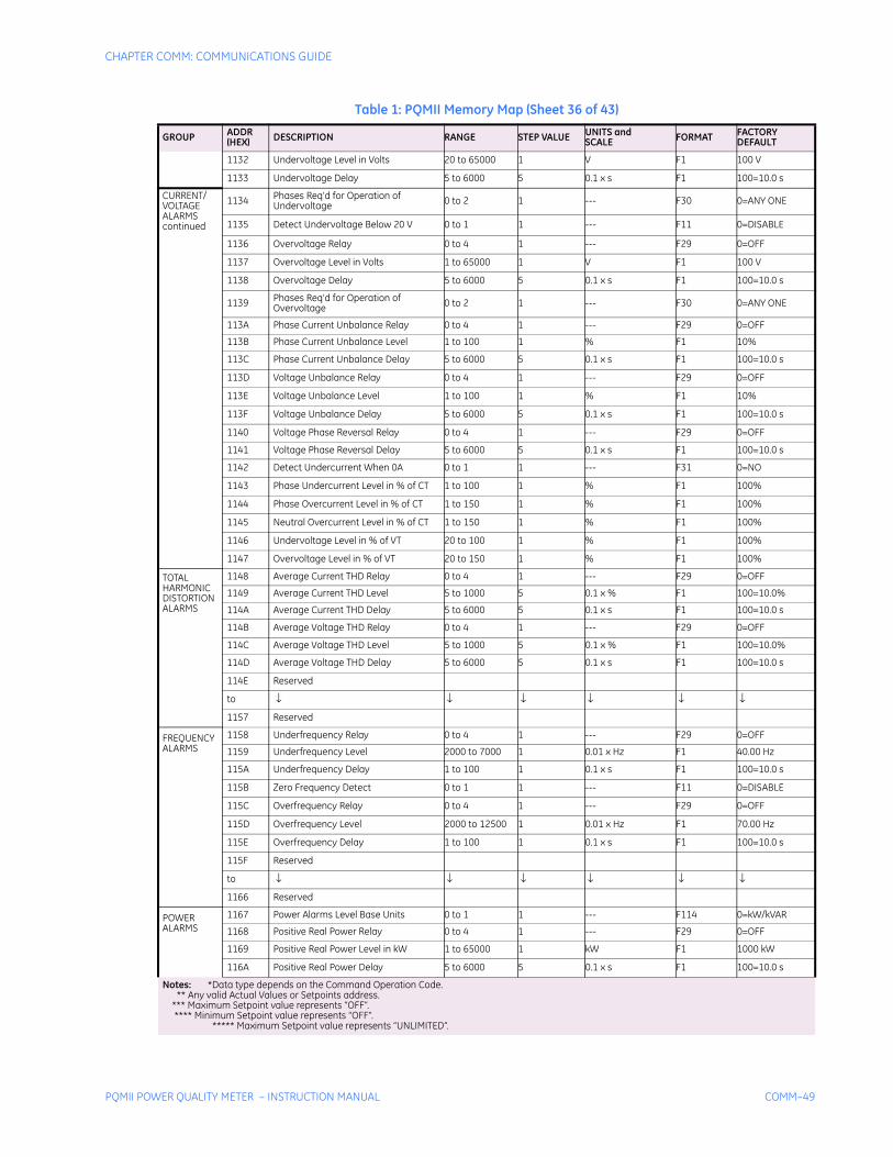
CHAPTER COMM: COMMUNICATIONS GUIDE
PQMII POWER QUALITY METER – INSTRUCTION MANUAL COMM–49
1132 Undervoltage Level in Volts 20 to 65000 1 V F1 100 V
1133 Undervoltage Delay 5 to 6000 5 0.1 x s F1 100=10.0 s
CURRENT/VOLTAGEALARMScontinued
1134 Phases Req’d for Operation of Undervoltage 0 to 2 1 --- F30 0=ANY ONE
1135 Detect Undervoltage Below 20 V 0 to 1 1 --- F11 0=DISABLE
1136 Overvoltage Relay 0 to 4 1 --- F29 0=OFF
1137 Overvoltage Level in Volts 1 to 65000 1 V F1 100 V
1138 Overvoltage Delay 5 to 6000 5 0.1 x s F1 100=10.0 s
1139 Phases Req’d for Operation of Overvoltage 0 to 2 1 --- F30 0=ANY ONE
113A Phase Current Unbalance Relay 0 to 4 1 --- F29 0=OFF
113B Phase Current Unbalance Level 1 to 100 1 % F1 10%
113C Phase Current Unbalance Delay 5 to 6000 5 0.1 x s F1 100=10.0 s
113D Voltage Unbalance Relay 0 to 4 1 --- F29 0=OFF
113E Voltage Unbalance Level 1 to 100 1 % F1 10%
113F Voltage Unbalance Delay 5 to 6000 5 0.1 x s F1 100=10.0 s
1140 Voltage Phase Reversal Relay 0 to 4 1 --- F29 0=OFF
1141 Voltage Phase Reversal Delay 5 to 6000 5 0.1 x s F1 100=10.0 s
1142 Detect Undercurrent When 0A 0 to 1 1 --- F31 0=NO
1143 Phase Undercurrent Level in % of CT 1 to 100 1 % F1 100%
1144 Phase Overcurrent Level in % of CT 1 to 150 1 % F1 100%
1145 Neutral Overcurrent Level in % of CT 1 to 150 1 % F1 100%
1146 Undervoltage Level in % of VT 20 to 100 1 % F1 100%
1147 Overvoltage Level in % of VT 20 to 150 1 % F1 100%
TOTALHARMONICDISTORTIONALARMS
1148 Average Current THD Relay 0 to 4 1 --- F29 0=OFF
1149 Average Current THD Level 5 to 1000 5 0.1 x % F1 100=10.0%
114A Average Current THD Delay 5 to 6000 5 0.1 x s F1 100=10.0 s
114B Average Voltage THD Relay 0 to 4 1 --- F29 0=OFF
114C Average Voltage THD Level 5 to 1000 5 0.1 x % F1 100=10.0%
114D Average Voltage THD Delay 5 to 6000 5 0.1 x s F1 100=10.0 s
114E Reserved
to ↓ ↓ ↓ ↓ ↓ ↓
1157 Reserved
FREQUENCYALARMS
1158 Underfrequency Relay 0 to 4 1 --- F29 0=OFF
1159 Underfrequency Level 2000 to 7000 1 0.01 x Hz F1 40.00 Hz
115A Underfrequency Delay 1 to 100 1 0.1 x s F1 100=10.0 s
115B Zero Frequency Detect 0 to 1 1 --- F11 0=DISABLE
115C Overfrequency Relay 0 to 4 1 --- F29 0=OFF
115D Overfrequency Level 2000 to 12500 1 0.01 x Hz F1 70.00 Hz
115E Overfrequency Delay 1 to 100 1 0.1 x s F1 100=10.0 s
115F Reserved
to ↓ ↓ ↓ ↓ ↓ ↓
1166 Reserved
POWERALARMS
1167 Power Alarms Level Base Units 0 to 1 1 --- F114 0=kW/kVAR
1168 Positive Real Power Relay 0 to 4 1 --- F29 0=OFF
1169 Positive Real Power Level in kW 1 to 65000 1 kW F1 1000 kW
116A Positive Real Power Delay 5 to 6000 5 0.1 x s F1 100=10.0 s
Table 1: PQMII Memory Map (Sheet 36 of 43)
GROUP ADDR(HEX) DESCRIPTION RANGE STEP VALUE UNITS and
SCALE FORMAT FACTORY DEFAULT
Notes: *Data type depends on the Command Operation Code. ** Any valid Actual Values or Setpoints address. *** Maximum Setpoint value represents “OFF”. **** Minimum Setpoint value represents “OFF”. ***** Maximum Setpoint value represents “UNLIMITED”.
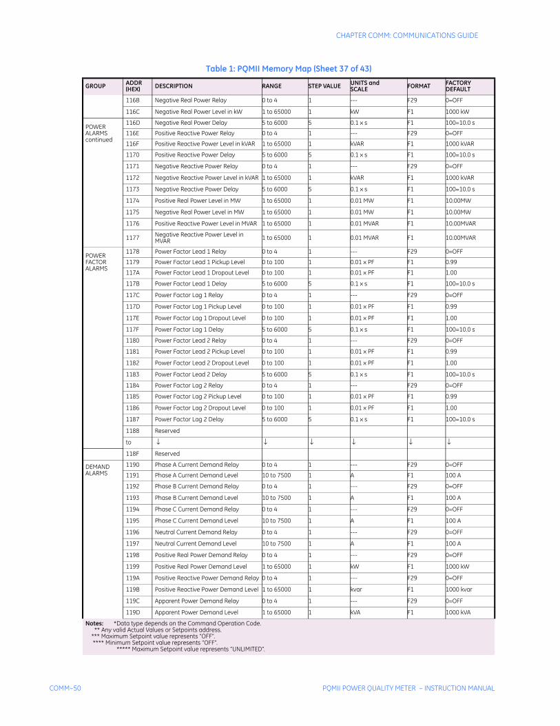
COMM–50 PQMII POWER QUALITY METER – INSTRUCTION MANUAL
CHAPTER COMM: COMMUNICATIONS GUIDE
116B Negative Real Power Relay 0 to 4 1 --- F29 0=OFF
116C Negative Real Power Level in kW 1 to 65000 1 kW F1 1000 kW
POWERALARMScontinued
116D Negative Real Power Delay 5 to 6000 5 0.1 x s F1 100=10.0 s
116E Positive Reactive Power Relay 0 to 4 1 --- F29 0=OFF
116F Positive Reactive Power Level in kVAR 1 to 65000 1 kVAR F1 1000 kVAR
1170 Positive Reactive Power Delay 5 to 6000 5 0.1 x s F1 100=10.0 s
1171 Negative Reactive Power Relay 0 to 4 1 --- F29 0=OFF
1172 Negative Reactive Power Level in kVAR 1 to 65000 1 kVAR F1 1000 kVAR
1173 Negative Reactive Power Delay 5 to 6000 5 0.1 x s F1 100=10.0 s
1174 Positive Real Power Level in MW 1 to 65000 1 0.01 MW F1 10.00MW
1175 Negative Real Power Level in MW 1 to 65000 1 0.01 MW F1 10.00MW
1176 Positive Reactive Power Level in MVAR 1 to 65000 1 0.01 MVAR F1 10.00MVAR
1177 Negative Reactive Power Level in MVAR 1 to 65000 1 0.01 MVAR F1 10.00MVAR
POWERFACTORALARMS
1178 Power Factor Lead 1 Relay 0 to 4 1 --- F29 0=OFF
1179 Power Factor Lead 1 Pickup Level 0 to 100 1 0.01 x PF F1 0.99
117A Power Factor Lead 1 Dropout Level 0 to 100 1 0.01 x PF F1 1.00
117B Power Factor Lead 1 Delay 5 to 6000 5 0.1 x s F1 100=10.0 s
117C Power Factor Lag 1 Relay 0 to 4 1 --- F29 0=OFF
117D Power Factor Lag 1 Pickup Level 0 to 100 1 0.01 x PF F1 0.99
117E Power Factor Lag 1 Dropout Level 0 to 100 1 0.01 x PF F1 1.00
117F Power Factor Lag 1 Delay 5 to 6000 5 0.1 x s F1 100=10.0 s
1180 Power Factor Lead 2 Relay 0 to 4 1 --- F29 0=OFF
1181 Power Factor Lead 2 Pickup Level 0 to 100 1 0.01 x PF F1 0.99
1182 Power Factor Lead 2 Dropout Level 0 to 100 1 0.01 x PF F1 1.00
1183 Power Factor Lead 2 Delay 5 to 6000 5 0.1 x s F1 100=10.0 s
1184 Power Factor Lag 2 Relay 0 to 4 1 --- F29 0=OFF
1185 Power Factor Lag 2 Pickup Level 0 to 100 1 0.01 x PF F1 0.99
1186 Power Factor Lag 2 Dropout Level 0 to 100 1 0.01 x PF F1 1.00
1187 Power Factor Lag 2 Delay 5 to 6000 5 0.1 x s F1 100=10.0 s
1188 Reserved
to ↓ ↓ ↓ ↓ ↓ ↓
118F Reserved
DEMANDALARMS
1190 Phase A Current Demand Relay 0 to 4 1 --- F29 0=OFF
1191 Phase A Current Demand Level 10 to 7500 1 A F1 100 A
1192 Phase B Current Demand Relay 0 to 4 1 --- F29 0=OFF
1193 Phase B Current Demand Level 10 to 7500 1 A F1 100 A
1194 Phase C Current Demand Relay 0 to 4 1 --- F29 0=OFF
1195 Phase C Current Demand Level 10 to 7500 1 A F1 100 A
1196 Neutral Current Demand Relay 0 to 4 1 --- F29 0=OFF
1197 Neutral Current Demand Level 10 to 7500 1 A F1 100 A
1198 Positive Real Power Demand Relay 0 to 4 1 --- F29 0=OFF
1199 Positive Real Power Demand Level 1 to 65000 1 kW F1 1000 kW
119A Positive Reactive Power Demand Relay 0 to 4 1 --- F29 0=OFF
119B Positive Reactive Power Demand Level 1 to 65000 1 kvar F1 1000 kvar
119C Apparent Power Demand Relay 0 to 4 1 --- F29 0=OFF
119D Apparent Power Demand Level 1 to 65000 1 kVA F1 1000 kVA
Table 1: PQMII Memory Map (Sheet 37 of 43)
GROUP ADDR(HEX) DESCRIPTION RANGE STEP VALUE UNITS and
SCALE FORMAT FACTORY DEFAULT
Notes: *Data type depends on the Command Operation Code. ** Any valid Actual Values or Setpoints address. *** Maximum Setpoint value represents “OFF”. **** Minimum Setpoint value represents “OFF”. ***** Maximum Setpoint value represents “UNLIMITED”.
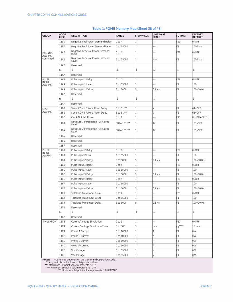
CHAPTER COMM: COMMUNICATIONS GUIDE
PQMII POWER QUALITY METER – INSTRUCTION MANUAL COMM–51
119E Negative Real Power Demand Relay 0 to 4 1 --- F29 0=OFF
119F Negative Real Power Demand Level 1 to 65000 1 kW F1 1000 kW
DEMANDALARMS continued
11A0 Negative Reactive Power Demand Relay 0 to 4 1 --- F29 0=OFF
11A1 Negative Reactive Power Demand Level 1 to 65000 1 kvar F1 1000 kvar
11A2 Reserved
to ↓ ↓ ↓ ↓ ↓ ↓
11A7 Reserved
PULSEINPUTALARMS
11A8 Pulse Input 1 Relay 0 to 4 1 --- F29 0=OFF
11A9 Pulse Input 1 Level 1 to 65000 1 --- F1 100
11AA Pulse Input 1 Delay 5 to 6000 5 0.1 x s F1 100=10.0 s
11AB Reserved
to ↓ ↓ ↓ ↓ ↓ ↓
11AF Reserved
MISC.ALARMS
11B0 Serial COM1 Failure Alarm Delay 5 to 61*** 1 s F1 61=OFF
11B1 Serial COM2 Failure Alarm Delay 5 to 61*** 1 s F1 61=OFF
11B2 Clock Not Set Alarm 0 to 1 1 --- F11 0 = DISABLED
11B3 Data Log 1 Percentage Full Alarm Level 50 to 101*** 1 % F1 101=OFF
11B4 Data Log 2 Percentage Full Alarm Level 50 to 101*** 1 % F1 101=OFF
11B5 Reserved
11B6 Reserved
11B7 Reserved
PULSEINPUTALARMS
11B8 Pulse Input 2 Relay 0 to 4 1 --- F29 0=OFF
11B9 Pulse Input 2 Level 1 to 65000 1 --- F1 100
11BA Pulse Input 2 Delay 5 to 6000 5 0.1 x s F1 100=10.0 s
11BB Pulse Input 3 Relay 0 to 4 1 --- F29 0=OFF
11BC Pulse Input 3 Level 1 to 65000 1 --- F1 100
11BD Pulse Input 3 Delay 5 to 6000 5 0.1 x s F1 100=10.0 s
11BE Pulse Input 4 Relay 0 to 4 1 --- F29 0=OFF
11BF Pulse Input 4 Level 1 to 65000 1 --- F1 100
11C0 Pulse Input 4 Delay 5 to 6000 5 0.1 x s F1 100=10.0 s
11C1 Totalized Pulse Input Relay 0 to 4 1 --- F29 0=OFF
11C2 Totalized Pulse Input Level 1 to 65000 1 --- F1 100
11C3 Totalized Pulse Input Delay 5 to 6000 5 0.1 x s F1 100=10.0 s
11C4 Reserved
to ↓ ↓ ↓ ↓ ↓ ↓
11C7 Reserved
SIMULATION 11C8 Current/Voltage Simulation 0 to 1 1 --- F11 0=OFF
11C9 Current/Voltage Simulation Time 5 to 305 5 min F1***** 15 min
11CA Phase A Current 0 to 10000 1 A F1 0 A
11CB Phase B Current 0 to 10000 1 A F1 0 A
11CC Phase C Current 0 to 10000 1 A F1 0 A
11CD Neutral Current 0 to 10000 1 A F1 0 A
11CE Vax Voltage 0 to 65000 1 V F1 0 V
11CF Vbx Voltage 0 to 65000 1 V F1 0 V
Table 1: PQMII Memory Map (Sheet 38 of 43)
GROUP ADDR(HEX) DESCRIPTION RANGE STEP VALUE UNITS and
SCALE FORMAT FACTORY DEFAULT
Notes: *Data type depends on the Command Operation Code. ** Any valid Actual Values or Setpoints address. *** Maximum Setpoint value represents “OFF”. **** Minimum Setpoint value represents “OFF”. ***** Maximum Setpoint value represents “UNLIMITED”.
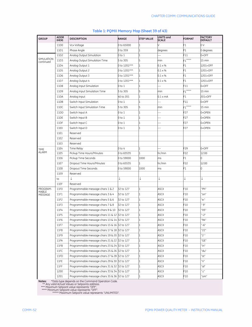
COMM–52 PQMII POWER QUALITY METER – INSTRUCTION MANUAL
CHAPTER COMM: COMMUNICATIONS GUIDE
11D0 Vcx Voltage 0 to 65000 1 V F1 0 V
11D1 Phase Angle 0 to 359 1 degrees F1 0 degrees
SIMULATION continued
11D2 Analog Output Simulation 0 to 1 1 --- F11 0=OFF
11D3 Analog Output Simulation Time 5 to 305 5 min F1***** 15 min
11D4 Analog Output 1 0 to 1201*** 1 0.1 x % F1 1201=OFF
11D5 Analog Output 2 0 to 1201*** 1 0.1 x % F1 1201=OFF
11D6 Analog Output 3 0 to 1201*** 1 0.1 x % F1 1201=OFF
11D7 Analog Output 4 0 to 1201*** 1 0.1 x % F1 1201=OFF
11D8 Analog Input Simulation 0 to 1 1 --- F11 0=OFF
11D9 Analog Input Simulation Time 5 to 305 5 min F1***** 15 min
11DA Analog Input 40 to 201 1 0.1 x mA F1 201=OFF
11DB Switch Input Simulation 0 to 1 1 --- F11 0=OFF
11DC Switch Input Simulation Time 5 to 305 5 min F1***** 15 min
11DD Switch Input A 0 to 1 1 --- F27 0=OPEN
11DE Switch Input B 0 to 1 1 --- F27 0=OPEN
11DF Switch Input C 0 to 1 1 --- F27 0=OPEN
11E0 Switch Input D 0 to 1 1 --- F27 0=OPEN
11E1 Reserved
11E2 Reserved
11E3 Reserved
TIMEALARM
11E4 Time Relay 0 to 4 1 --- F29 0=OFF
11E5 Pickup Time Hours/Minutes 0 to 65535 1 hr./min F22 12:00
11E6 Pickup Time Seconds 0 to 59000 1000 ms F1 0
11E7 Dropout Time Hours/Minutes 0 to 65535 1 hr./min F22 12:00
11E8 Dropout Time Seconds 0 to 59000 1000 ms F1 0
11E9 Reserved
to ↓ ↓ ↓ ↓ ↓ ↓
11EF Reserved
PROGRAM-MABLEMESSAGE
11F0 Programmable message chars 1 & 2 32 to 127 1 ASCII F10 “Ph”
11F1 Programmable message chars 3 & 4 32 to 127 1 ASCII F10 “on”
11F2 Programmable message chars 5 & 6 32 to 127 1 ASCII F10 “e:”
11F3 Programmable message chars 7 & 8 32 to 127 1 ASCII F10 “ 9”
11F4 Programmable message chars 9 & 10 32 to 127 1 ASCII F10 “05”
11F5 Programmable message chars 11 & 12 32 to 127 1 ASCII F10 “-2”
11F6 Programmable message chars 13 & 14 32 to 127 1 ASCII F10 “94”
11F7 Programmable message chars 15 & 16 32 to 127 1 ASCII F10 “-6”
11F8 Programmable message chars 17 & 18 32 to 127 1 ASCII F10 “22”
11F9 Programmable message chars 19 & 20 32 to 127 1 ASCII F10 “2 ”
11FA Programmable message chars 21 & 22 32 to 127 1 ASCII F10 “GE”
11FB Programmable message chars 23 & 24 32 to 127 1 ASCII F10 “in”
11FC Programmable message chars 25 & 26 32 to 127 1 ASCII F10 “du”
11FD Programmable message chars 27 & 28 32 to 127 1 ASCII F10 “st”
11FE Programmable message chars 29 & 30 32 to 127 1 ASCII F10 “ri”
11FF Programmable message chars 31 & 32 32 to 127 1 ASCII F10 “al”
1200 Programmable message chars 33 & 34 32 to 127 1 ASCII F10 “.c”
1201 Programmable message chars 35 & 36 32 to 127 1 ASCII F10 “om”
Table 1: PQMII Memory Map (Sheet 39 of 43)
GROUP ADDR(HEX) DESCRIPTION RANGE STEP VALUE UNITS and
SCALE FORMAT FACTORY DEFAULT
Notes: *Data type depends on the Command Operation Code. ** Any valid Actual Values or Setpoints address. *** Maximum Setpoint value represents “OFF”. **** Minimum Setpoint value represents “OFF”. ***** Maximum Setpoint value represents “UNLIMITED”.
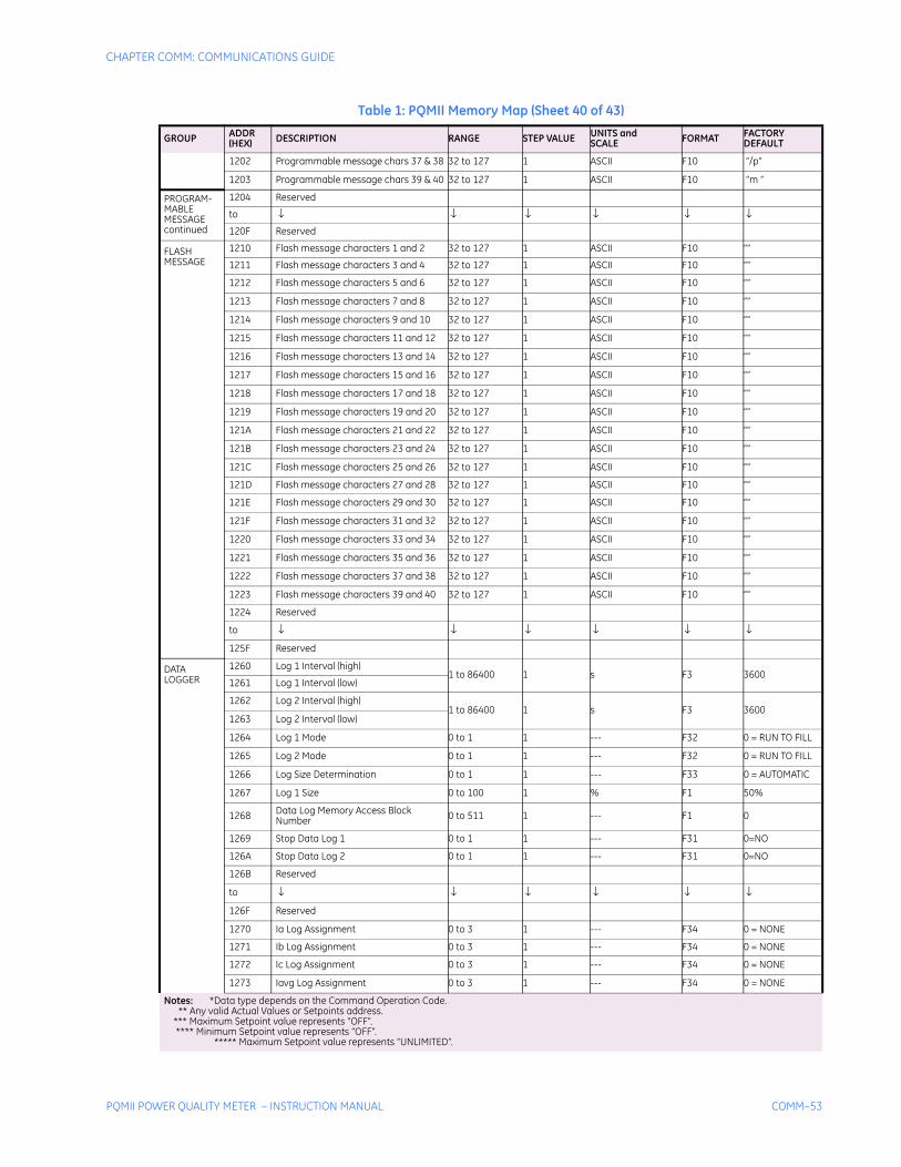
CHAPTER COMM: COMMUNICATIONS GUIDE
PQMII POWER QUALITY METER – INSTRUCTION MANUAL COMM–53
1202 Programmable message chars 37 & 38 32 to 127 1 ASCII F10 “/p”
1203 Programmable message chars 39 & 40 32 to 127 1 ASCII F10 “m ”
PROGRAM-MABLE MESSAGE continued
1204 Reserved
to ↓ ↓ ↓ ↓ ↓ ↓
120F Reserved
FLASHMESSAGE
1210 Flash message characters 1 and 2 32 to 127 1 ASCII F10 “”
1211 Flash message characters 3 and 4 32 to 127 1 ASCII F10 “”
1212 Flash message characters 5 and 6 32 to 127 1 ASCII F10 “”
1213 Flash message characters 7 and 8 32 to 127 1 ASCII F10 “”
1214 Flash message characters 9 and 10 32 to 127 1 ASCII F10 “”
1215 Flash message characters 11 and 12 32 to 127 1 ASCII F10 “”
1216 Flash message characters 13 and 14 32 to 127 1 ASCII F10 “”
1217 Flash message characters 15 and 16 32 to 127 1 ASCII F10 “”
1218 Flash message characters 17 and 18 32 to 127 1 ASCII F10 “”
1219 Flash message characters 19 and 20 32 to 127 1 ASCII F10 “”
121A Flash message characters 21 and 22 32 to 127 1 ASCII F10 “”
121B Flash message characters 23 and 24 32 to 127 1 ASCII F10 “”
121C Flash message characters 25 and 26 32 to 127 1 ASCII F10 “”
121D Flash message characters 27 and 28 32 to 127 1 ASCII F10 “”
121E Flash message characters 29 and 30 32 to 127 1 ASCII F10 “”
121F Flash message characters 31 and 32 32 to 127 1 ASCII F10 “”
1220 Flash message characters 33 and 34 32 to 127 1 ASCII F10 “”
1221 Flash message characters 35 and 36 32 to 127 1 ASCII F10 “”
1222 Flash message characters 37 and 38 32 to 127 1 ASCII F10 “”
1223 Flash message characters 39 and 40 32 to 127 1 ASCII F10 “”
1224 Reserved
to ↓ ↓ ↓ ↓ ↓ ↓
125F Reserved
DATALOGGER
1260 Log 1 Interval (high)1 to 86400 1 s F3 3600
1261 Log 1 Interval (low)
1262 Log 2 Interval (high)1 to 86400 1 s F3 3600
1263 Log 2 Interval (low)
1264 Log 1 Mode 0 to 1 1 --- F32 0 = RUN TO FILL
1265 Log 2 Mode 0 to 1 1 --- F32 0 = RUN TO FILL
1266 Log Size Determination 0 to 1 1 --- F33 0 = AUTOMATIC
1267 Log 1 Size 0 to 100 1 % F1 50%
1268 Data Log Memory Access Block Number 0 to 511 1 --- F1 0
1269 Stop Data Log 1 0 to 1 1 --- F31 0=NO
126A Stop Data Log 2 0 to 1 1 --- F31 0=NO
126B Reserved
to ↓ ↓ ↓ ↓ ↓ ↓
126F Reserved
1270 Ia Log Assignment 0 to 3 1 --- F34 0 = NONE
1271 Ib Log Assignment 0 to 3 1 --- F34 0 = NONE
1272 Ic Log Assignment 0 to 3 1 --- F34 0 = NONE
1273 Iavg Log Assignment 0 to 3 1 --- F34 0 = NONE
Table 1: PQMII Memory Map (Sheet 40 of 43)
GROUP ADDR(HEX) DESCRIPTION RANGE STEP VALUE UNITS and
SCALE FORMAT FACTORY DEFAULT
Notes: *Data type depends on the Command Operation Code. ** Any valid Actual Values or Setpoints address. *** Maximum Setpoint value represents “OFF”. **** Minimum Setpoint value represents “OFF”. ***** Maximum Setpoint value represents “UNLIMITED”.
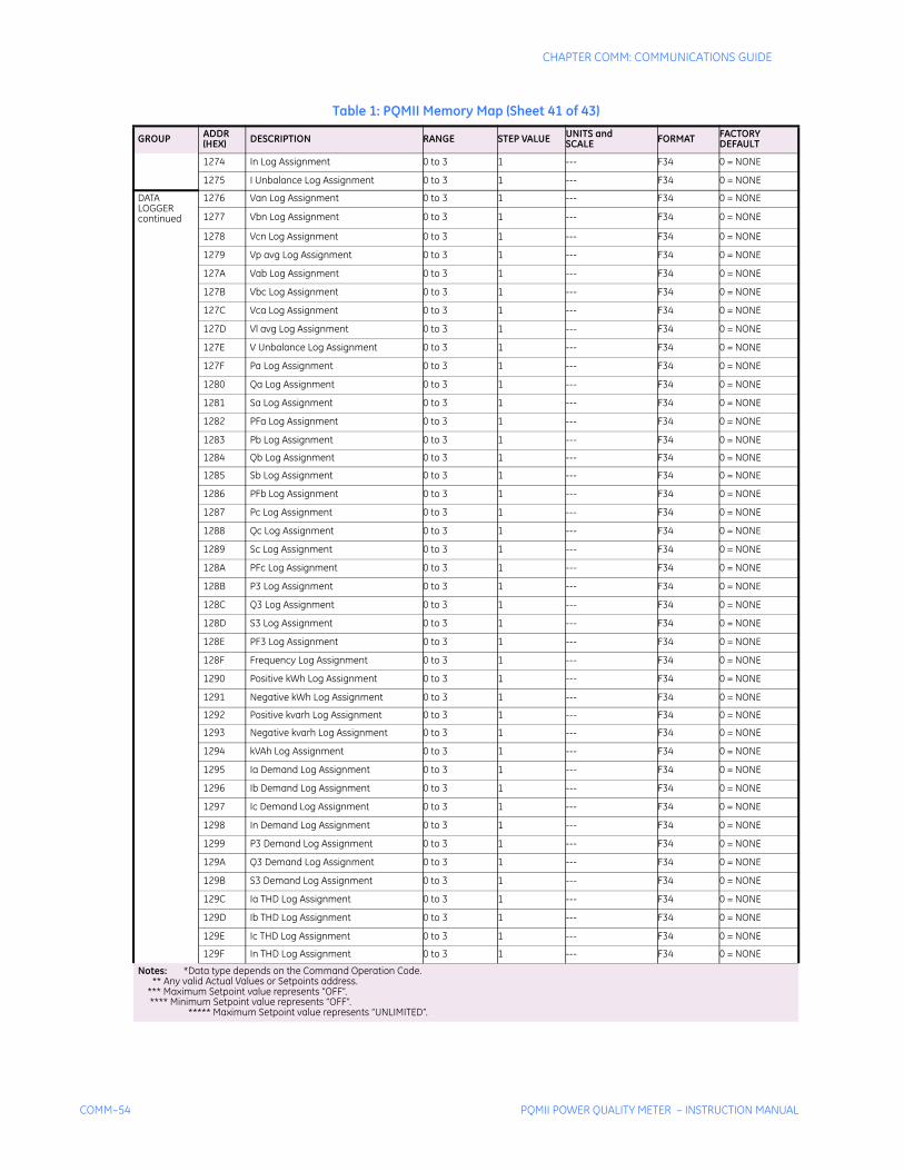
COMM–54 PQMII POWER QUALITY METER – INSTRUCTION MANUAL
CHAPTER COMM: COMMUNICATIONS GUIDE
1274 In Log Assignment 0 to 3 1 --- F34 0 = NONE
1275 I Unbalance Log Assignment 0 to 3 1 --- F34 0 = NONE
DATALOGGER continued
1276 Van Log Assignment 0 to 3 1 --- F34 0 = NONE
1277 Vbn Log Assignment 0 to 3 1 --- F34 0 = NONE
1278 Vcn Log Assignment 0 to 3 1 --- F34 0 = NONE
1279 Vp avg Log Assignment 0 to 3 1 --- F34 0 = NONE
127A Vab Log Assignment 0 to 3 1 --- F34 0 = NONE
127B Vbc Log Assignment 0 to 3 1 --- F34 0 = NONE
127C Vca Log Assignment 0 to 3 1 --- F34 0 = NONE
127D Vl avg Log Assignment 0 to 3 1 --- F34 0 = NONE
127E V Unbalance Log Assignment 0 to 3 1 --- F34 0 = NONE
127F Pa Log Assignment 0 to 3 1 --- F34 0 = NONE
1280 Qa Log Assignment 0 to 3 1 --- F34 0 = NONE
1281 Sa Log Assignment 0 to 3 1 --- F34 0 = NONE
1282 PFa Log Assignment 0 to 3 1 --- F34 0 = NONE
1283 Pb Log Assignment 0 to 3 1 --- F34 0 = NONE
1284 Qb Log Assignment 0 to 3 1 --- F34 0 = NONE
1285 Sb Log Assignment 0 to 3 1 --- F34 0 = NONE
1286 PFb Log Assignment 0 to 3 1 --- F34 0 = NONE
1287 Pc Log Assignment 0 to 3 1 --- F34 0 = NONE
1288 Qc Log Assignment 0 to 3 1 --- F34 0 = NONE
1289 Sc Log Assignment 0 to 3 1 --- F34 0 = NONE
128A PFc Log Assignment 0 to 3 1 --- F34 0 = NONE
128B P3 Log Assignment 0 to 3 1 --- F34 0 = NONE
128C Q3 Log Assignment 0 to 3 1 --- F34 0 = NONE
128D S3 Log Assignment 0 to 3 1 --- F34 0 = NONE
128E PF3 Log Assignment 0 to 3 1 --- F34 0 = NONE
128F Frequency Log Assignment 0 to 3 1 --- F34 0 = NONE
1290 Positive kWh Log Assignment 0 to 3 1 --- F34 0 = NONE
1291 Negative kWh Log Assignment 0 to 3 1 --- F34 0 = NONE
1292 Positive kvarh Log Assignment 0 to 3 1 --- F34 0 = NONE
1293 Negative kvarh Log Assignment 0 to 3 1 --- F34 0 = NONE
1294 kVAh Log Assignment 0 to 3 1 --- F34 0 = NONE
1295 Ia Demand Log Assignment 0 to 3 1 --- F34 0 = NONE
1296 Ib Demand Log Assignment 0 to 3 1 --- F34 0 = NONE
1297 Ic Demand Log Assignment 0 to 3 1 --- F34 0 = NONE
1298 In Demand Log Assignment 0 to 3 1 --- F34 0 = NONE
1299 P3 Demand Log Assignment 0 to 3 1 --- F34 0 = NONE
129A Q3 Demand Log Assignment 0 to 3 1 --- F34 0 = NONE
129B S3 Demand Log Assignment 0 to 3 1 --- F34 0 = NONE
129C Ia THD Log Assignment 0 to 3 1 --- F34 0 = NONE
129D Ib THD Log Assignment 0 to 3 1 --- F34 0 = NONE
129E Ic THD Log Assignment 0 to 3 1 --- F34 0 = NONE
129F In THD Log Assignment 0 to 3 1 --- F34 0 = NONE
Table 1: PQMII Memory Map (Sheet 41 of 43)
GROUP ADDR(HEX) DESCRIPTION RANGE STEP VALUE UNITS and
SCALE FORMAT FACTORY DEFAULT
Notes: *Data type depends on the Command Operation Code. ** Any valid Actual Values or Setpoints address. *** Maximum Setpoint value represents “OFF”. **** Minimum Setpoint value represents “OFF”. ***** Maximum Setpoint value represents “UNLIMITED”.
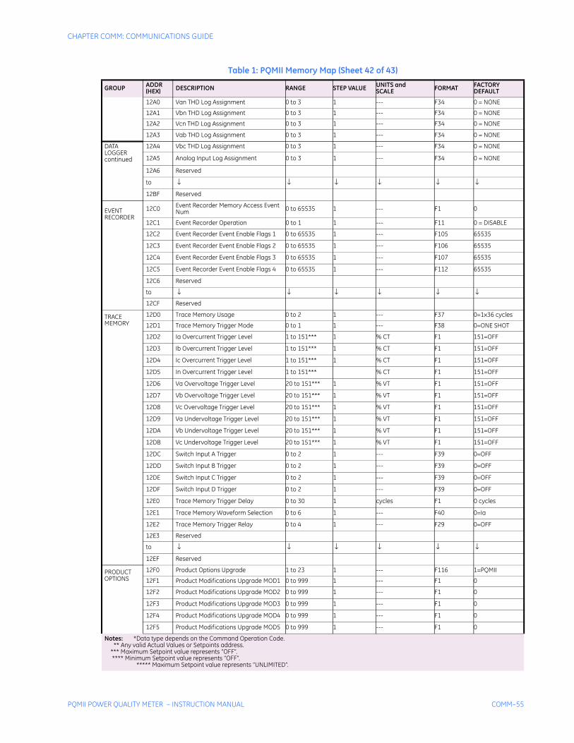
CHAPTER COMM: COMMUNICATIONS GUIDE
PQMII POWER QUALITY METER – INSTRUCTION MANUAL COMM–55
12A0 Van THD Log Assignment 0 to 3 1 --- F34 0 = NONE
12A1 Vbn THD Log Assignment 0 to 3 1 --- F34 0 = NONE
12A2 Vcn THD Log Assignment 0 to 3 1 --- F34 0 = NONE
12A3 Vab THD Log Assignment 0 to 3 1 --- F34 0 = NONE
DATALOGGERcontinued
12A4 Vbc THD Log Assignment 0 to 3 1 --- F34 0 = NONE
12A5 Analog Input Log Assignment 0 to 3 1 --- F34 0 = NONE
12A6 Reserved
to ↓ ↓ ↓ ↓ ↓ ↓
12BF Reserved
EVENTRECORDER
12C0 Event Recorder Memory Access Event Num 0 to 65535 1 --- F1 0
12C1 Event Recorder Operation 0 to 1 1 --- F11 0 = DISABLE
12C2 Event Recorder Event Enable Flags 1 0 to 65535 1 --- F105 65535
12C3 Event Recorder Event Enable Flags 2 0 to 65535 1 --- F106 65535
12C4 Event Recorder Event Enable Flags 3 0 to 65535 1 --- F107 65535
12C5 Event Recorder Event Enable Flags 4 0 to 65535 1 --- F112 65535
12C6 Reserved
to ↓ ↓ ↓ ↓ ↓ ↓
12CF Reserved
TRACEMEMORY
12D0 Trace Memory Usage 0 to 2 1 --- F37 0=1x36 cycles
12D1 Trace Memory Trigger Mode 0 to 1 1 --- F38 0=ONE SHOT
12D2 Ia Overcurrent Trigger Level 1 to 151*** 1 % CT F1 151=OFF
12D3 Ib Overcurrent Trigger Level 1 to 151*** 1 % CT F1 151=OFF
12D4 Ic Overcurrent Trigger Level 1 to 151*** 1 % CT F1 151=OFF
12D5 In Overcurrent Trigger Level 1 to 151*** % CT F1 151=OFF
12D6 Va Overvoltage Trigger Level 20 to 151*** 1 % VT F1 151=OFF
12D7 Vb Overvoltage Trigger Level 20 to 151*** 1 % VT F1 151=OFF
12D8 Vc Overvoltage Trigger Level 20 to 151*** 1 % VT F1 151=OFF
12D9 Va Undervoltage Trigger Level 20 to 151*** 1 % VT F1 151=OFF
12DA Vb Undervoltage Trigger Level 20 to 151*** 1 % VT F1 151=OFF
12DB Vc Undervoltage Trigger Level 20 to 151*** 1 % VT F1 151=OFF
12DC Switch Input A Trigger 0 to 2 1 --- F39 0=OFF
12DD Switch Input B Trigger 0 to 2 1 --- F39 0=OFF
12DE Switch Input C Trigger 0 to 2 1 --- F39 0=OFF
12DF Switch Input D Trigger 0 to 2 1 --- F39 0=OFF
12E0 Trace Memory Trigger Delay 0 to 30 1 cycles F1 0 cycles
12E1 Trace Memory Waveform Selection 0 to 6 1 --- F40 0=Ia
12E2 Trace Memory Trigger Relay 0 to 4 1 --- F29 0=OFF
12E3 Reserved
to ↓ ↓ ↓ ↓ ↓ ↓
12EF Reserved
PRODUCTOPTIONS
12F0 Product Options Upgrade 1 to 23 1 --- F116 1=PQMII
12F1 Product Modifications Upgrade MOD1 0 to 999 1 --- F1 0
12F2 Product Modifications Upgrade MOD2 0 to 999 1 --- F1 0
12F3 Product Modifications Upgrade MOD3 0 to 999 1 --- F1 0
12F4 Product Modifications Upgrade MOD4 0 to 999 1 --- F1 0
12F5 Product Modifications Upgrade MOD5 0 to 999 1 --- F1 0
Table 1: PQMII Memory Map (Sheet 42 of 43)
GROUP ADDR(HEX) DESCRIPTION RANGE STEP VALUE UNITS and
SCALE FORMAT FACTORY DEFAULT
Notes: *Data type depends on the Command Operation Code. ** Any valid Actual Values or Setpoints address. *** Maximum Setpoint value represents “OFF”. **** Minimum Setpoint value represents “OFF”. ***** Maximum Setpoint value represents “UNLIMITED”.
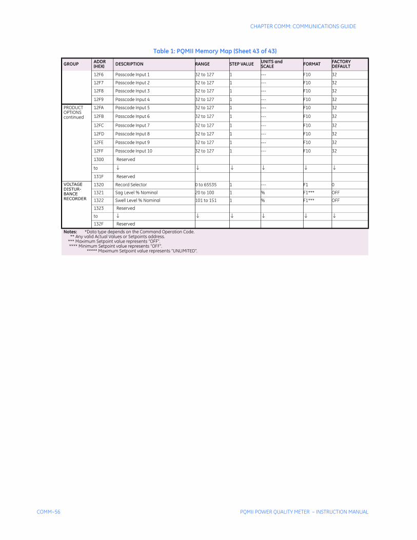
COMM–56 PQMII POWER QUALITY METER – INSTRUCTION MANUAL
CHAPTER COMM: COMMUNICATIONS GUIDE
12F6 Passcode Input 1 32 to 127 1 --- F10 32
12F7 Passcode Input 2 32 to 127 1 --- F10 32
12F8 Passcode Input 3 32 to 127 1 --- F10 32
12F9 Passcode Input 4 32 to 127 1 --- F10 32
PRODUCTOPTIONS continued
12FA Passcode Input 5 32 to 127 1 --- F10 32
12FB Passcode Input 6 32 to 127 1 --- F10 32
12FC Passcode Input 7 32 to 127 1 --- F10 32
12FD Passcode Input 8 32 to 127 1 --- F10 32
12FE Passcode Input 9 32 to 127 1 --- F10 32
12FF Passcode Input 10 32 to 127 1 --- F10 32
1300 Reserved
to ↓ ↓ ↓ ↓ ↓ ↓
131F Reserved
VOLTAGEDISTUR-BANCERECORDER
1320 Record Selector 0 to 65535 1 --- F1 0
1321 Sag Level % Nominal 20 to 100 1 % F1*** OFF
1322 Swell Level % Nominal 101 to 151 1 % F1*** OFF
1323 Reserved
to ↓ ↓ ↓ ↓ ↓ ↓
132F Reserved
Table 1: PQMII Memory Map (Sheet 43 of 43)
GROUP ADDR(HEX) DESCRIPTION RANGE STEP VALUE UNITS and
SCALE FORMAT FACTORY DEFAULT
Notes: *Data type depends on the Command Operation Code. ** Any valid Actual Values or Setpoints address. *** Maximum Setpoint value represents “OFF”. **** Minimum Setpoint value represents “OFF”. ***** Maximum Setpoint value represents “UNLIMITED”.
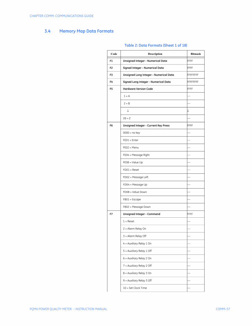
CHAPTER COMM: COMMUNICATIONS GUIDE
PQMII POWER QUALITY METER – INSTRUCTION MANUAL COMM–57
3.4 Memory Map Data Formats
Table 2: Data Formats (Sheet 1 of 18)
Code Description Bitmask
F1 Unsigned Integer - Numerical Data FFFF
F2 Signed Integer - Numerical Data FFFF
F3 Unsigned Long Integer - Numerical Data FFFFFFFF
F4 Signed Long Integer - Numerical Data FFFFFFFF
F5 Hardware Version Code FFFF
1 = A ---
2 = B ---
↓ ↓
26 = Z ---
F6 Unsigned Integer - Current Key Press FFFF
0000 = no key ---
FE01 = Enter ---
FE02 = Menu ---
FE04 = Message Right ---
FE08 = Value Up ---
FD01 = Reset ---
FD02 = Message Left ---
FD04 = Message Up ---
FD08 = Value Down ---
FB01 = Escape ---
FB02 = Message Down ---
F7 Unsigned Integer - Command FFFF
1 = Reset ---
2 = Alarm Relay On ---
3 = Alarm Relay Off ---
4 = Auxiliary Relay 1 On ---
5 = Auxiliary Relay 1 Off ---
6 = Auxiliary Relay 2 On ---
7 = Auxiliary Relay 2 Off ---
8 = Auxiliary Relay 3 On ---
9 = Auxiliary Relay 3 Off ---
10 = Set Clock Time ---
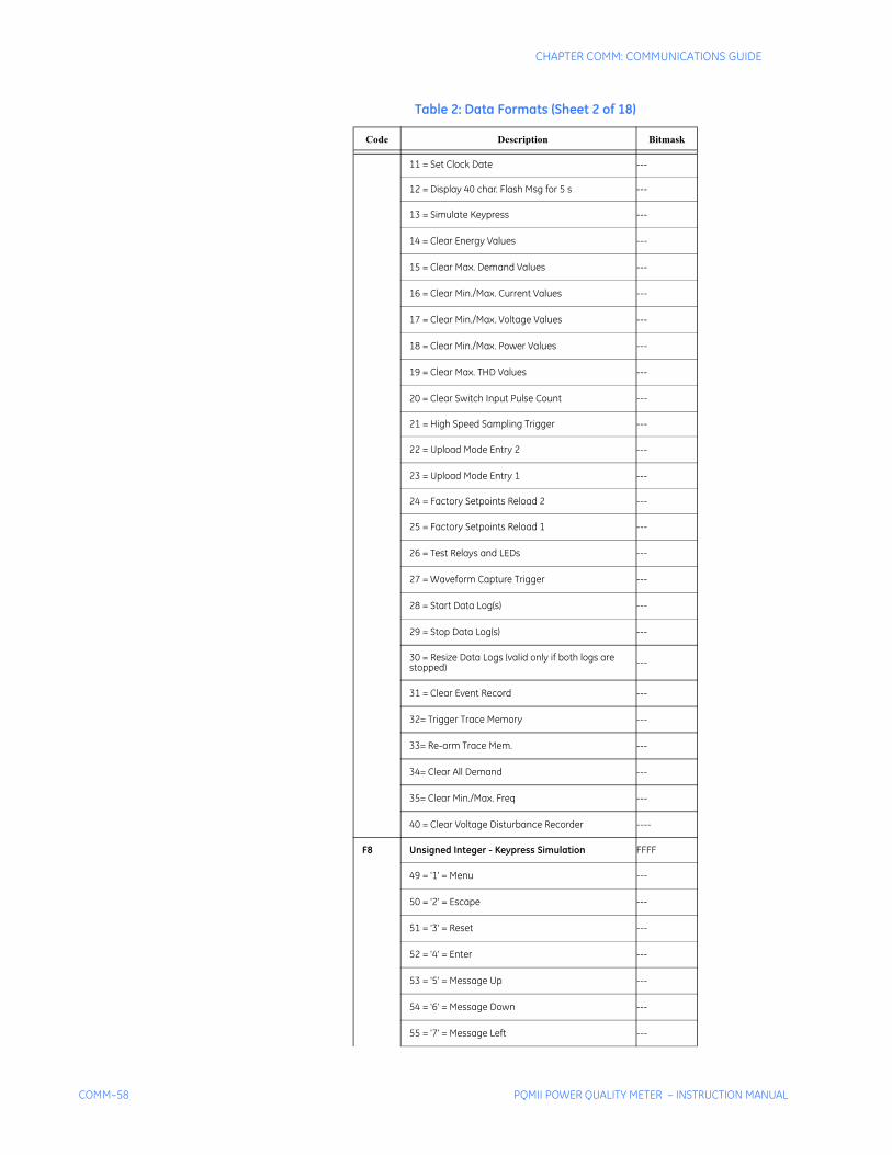
COMM–58 PQMII POWER QUALITY METER – INSTRUCTION MANUAL
CHAPTER COMM: COMMUNICATIONS GUIDE
11 = Set Clock Date ---
12 = Display 40 char. Flash Msg for 5 s ---
13 = Simulate Keypress ---
14 = Clear Energy Values ---
15 = Clear Max. Demand Values ---
16 = Clear Min./Max. Current Values ---
17 = Clear Min./Max. Voltage Values ---
18 = Clear Min./Max. Power Values ---
19 = Clear Max. THD Values ---
20 = Clear Switch Input Pulse Count ---
21 = High Speed Sampling Trigger ---
22 = Upload Mode Entry 2 ---
23 = Upload Mode Entry 1 ---
24 = Factory Setpoints Reload 2 ---
25 = Factory Setpoints Reload 1 ---
26 = Test Relays and LEDs ---
27 = Waveform Capture Trigger ---
28 = Start Data Log(s) ---
29 = Stop Data Log(s) ---
30 = Resize Data Logs (valid only if both logs are stopped) ---
31 = Clear Event Record ---
32= Trigger Trace Memory ---
33= Re-arm Trace Mem. ---
34= Clear All Demand ---
35= Clear Min./Max. Freq ---
40 = Clear Voltage Disturbance Recorder ----
F8 Unsigned Integer - Keypress Simulation FFFF
49 = '1' = Menu ---
50 = '2' = Escape ---
51 = '3' = Reset ---
52 = '4' = Enter ---
53 = '5' = Message Up ---
54 = '6' = Message Down ---
55 = '7' = Message Left ---
Table 2: Data Formats (Sheet 2 of 18)
Code Description Bitmask
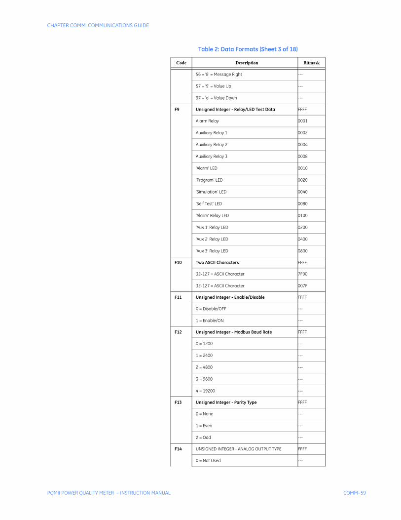
CHAPTER COMM: COMMUNICATIONS GUIDE
PQMII POWER QUALITY METER – INSTRUCTION MANUAL COMM–59
56 = '8' = Message Right ---
57 = '9' = Value Up ---
97 = 'a' = Value Down ---
F9 Unsigned Integer - Relay/LED Test Data FFFF
Alarm Relay 0001
Auxiliary Relay 1 0002
Auxiliary Relay 2 0004
Auxiliary Relay 3 0008
‘Alarm’ LED 0010
‘Program’ LED 0020
‘Simulation’ LED 0040
‘Self Test’ LED 0080
‘Alarm’ Relay LED 0100
‘Aux 1’ Relay LED 0200
‘Aux 2’ Relay LED 0400
‘Aux 3’ Relay LED 0800
F10 Two ASCII Characters FFFF
32-127 = ASCII Character 7F00
32-127 = ASCII Character 007F
F11 Unsigned Integer - Enable/Disable FFFF
0 = Disable/OFF ---
1 = Enable/ON ---
F12 Unsigned Integer - Modbus Baud Rate FFFF
0 = 1200 ---
1 = 2400 ---
2 = 4800 ---
3 = 9600 ---
4 = 19200 ---
F13 Unsigned Integer - Parity Type FFFF
0 = None ---
1 = Even ---
2 = Odd ---
F14 UNSIGNED INTEGER - ANALOG OUTPUT TYPE FFFF
0 = Not Used ---
Table 2: Data Formats (Sheet 3 of 18)
Code Description Bitmask
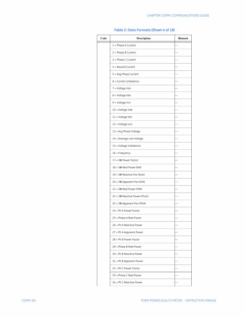
COMM–60 PQMII POWER QUALITY METER – INSTRUCTION MANUAL
CHAPTER COMM: COMMUNICATIONS GUIDE
1 = Phase A Current ---
2 = Phase B Current ---
3 = Phase C Current ---
4 = Neutral Current ---
5 = Avg Phase Current ---
6 = Current Unbalance ---
7 = Voltage Van ---
8 = Voltage Vbn ---
9 = Voltage Vcn ---
10 = Voltage Vab ---
11 = Voltage Vbc ---
12 = Voltage Vca ---
13 = Avg Phase Voltage ---
14 = Average Line Voltage ---
15 = Voltage Unbalance ---
16 = Frequency ---
17 = 3Φ Power Factor ---
18 = 3Φ Real Power (kW) ---
19 = 3Φ Reactive Pwr (kvar) ---
20 = 3Φ Apparent Pwr (kVA) ---
21 = 3Φ Real Power (MW) ---
22 = 3Φ Reactive Power (Mvar) ---
23 = 3Φ Apparent Pwr (MVA) ---
24 = Ph A Power Factor ---
25 = Phase A Real Power ---
26 = Ph A Reactive Power ---
27 = Ph A Apparent Power ---
28 = Ph B Power Factor ---
29 = Phase B Real Power ---
30 = Ph B Reactive Power ---
31 = Ph B Apparent Power ---
32 = Ph C Power Factor ---
33 = Phase C Real Power ---
34 = Ph C Reactive Power ---
Table 2: Data Formats (Sheet 4 of 18)
Code Description Bitmask
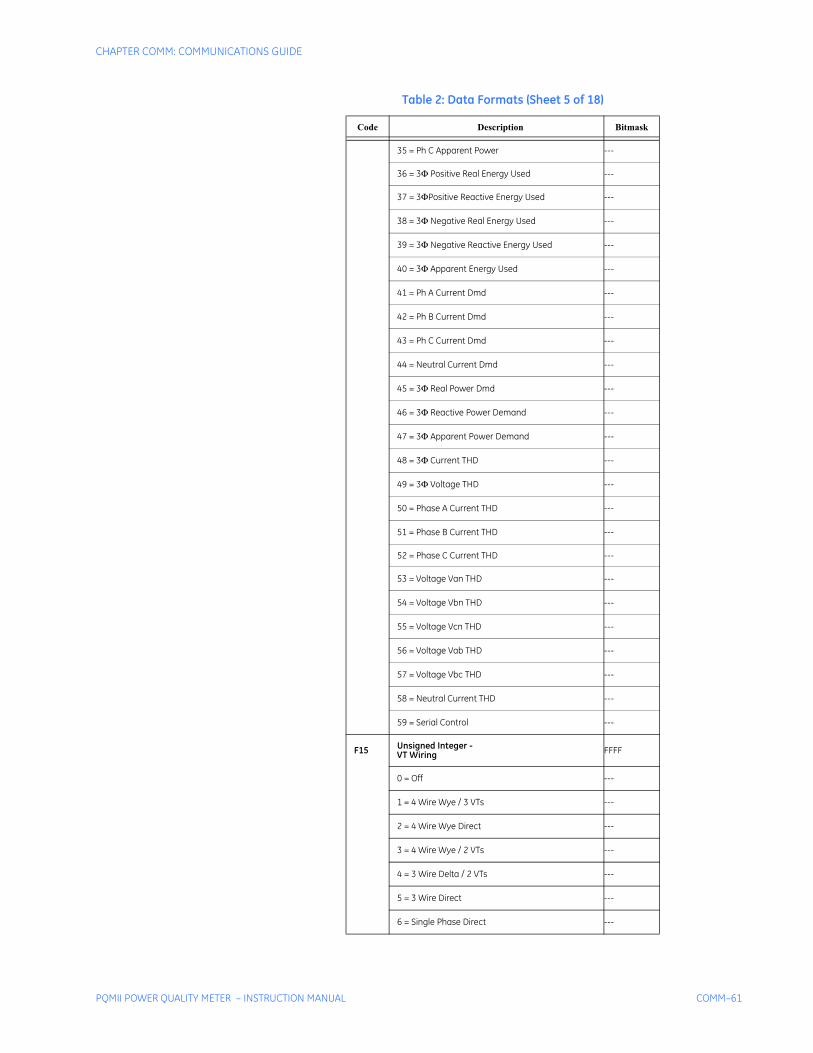
CHAPTER COMM: COMMUNICATIONS GUIDE
PQMII POWER QUALITY METER – INSTRUCTION MANUAL COMM–61
35 = Ph C Apparent Power ---
36 = 3Φ Positive Real Energy Used ---
37 = 3ΦPositive Reactive Energy Used ---
38 = 3Φ Negative Real Energy Used ---
39 = 3Φ Negative Reactive Energy Used ---
40 = 3Φ Apparent Energy Used ---
41 = Ph A Current Dmd ---
42 = Ph B Current Dmd ---
43 = Ph C Current Dmd ---
44 = Neutral Current Dmd ---
45 = 3Φ Real Power Dmd ---
46 = 3Φ Reactive Power Demand ---
47 = 3Φ Apparent Power Demand ---
48 = 3Φ Current THD ---
49 = 3Φ Voltage THD ---
50 = Phase A Current THD ---
51 = Phase B Current THD ---
52 = Phase C Current THD ---
53 = Voltage Van THD ---
54 = Voltage Vbn THD ---
55 = Voltage Vcn THD ---
56 = Voltage Vab THD ---
57 = Voltage Vbc THD ---
58 = Neutral Current THD ---
59 = Serial Control ---
F15 Unsigned Integer -VT Wiring FFFF
0 = Off ---
1 = 4 Wire Wye / 3 VTs ---
2 = 4 Wire Wye Direct ---
3 = 4 Wire Wye / 2 VTs ---
4 = 3 Wire Delta / 2 VTs ---
5 = 3 Wire Direct ---
6 = Single Phase Direct ---
Table 2: Data Formats (Sheet 5 of 18)
Code Description Bitmask
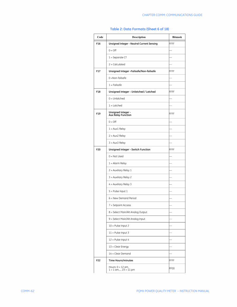
COMM–62 PQMII POWER QUALITY METER – INSTRUCTION MANUAL
CHAPTER COMM: COMMUNICATIONS GUIDE
F16 Unsigned Integer - Neutral Current Sensing FFFF
0 = Off ---
1 = Separate CT ---
2 = Calculated ---
F17 Unsigned Integer -Failsafe/Non-failsafe FFFF
0 =Non-failsafe ---
1 = Failsafe ---
F18 Unsigned Integer - Unlatched / Latched FFFF
0 = Unlatched ---
1 = Latched ---
F19 Unsigned Integer -Aux Relay Function FFFF
0 = Off ---
1 = Aux1 Relay ---
2 = Aux2 Relay ---
3 = Aux3 Relay ---
F20 Unsigned Integer - Switch Function FFFF
0 = Not Used ---
1 = Alarm Relay ---
2 = Auxiliary Relay 1 ---
3 = Auxiliary Relay 2 ---
4 = Auxiliary Relay 3 ---
5 = Pulse Input 1 ---
6 = New Demand Period ---
7 = Setpoint Access ---
8 = Select Main/Alt Analog Output ---
9 = Select Main/Alt Analog Input ---
10 = Pulse Input 2 ---
11 = Pulse Input 3 ---
12 = Pulse Input 4 ---
13 = Clear Energy ---
14 = Clear Demand ---
F22 Time Hours/minutes FFFF
Hours: 0 = 12 am,1 = 1 am,..., 23 = 11 pm FF00
Table 2: Data Formats (Sheet 6 of 18)
Code Description Bitmask
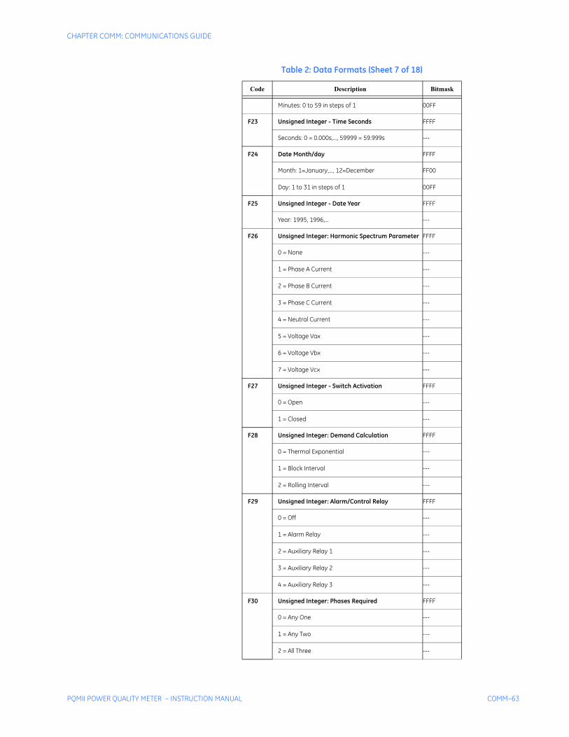
CHAPTER COMM: COMMUNICATIONS GUIDE
PQMII POWER QUALITY METER – INSTRUCTION MANUAL COMM–63
Minutes: 0 to 59 in steps of 1 00FF
F23 Unsigned Integer - Time Seconds FFFF
Seconds: 0 = 0.000s,..., 59999 = 59.999s ---
F24 Date Month/day FFFF
Month: 1=January,..., 12=December FF00
Day: 1 to 31 in steps of 1 00FF
F25 Unsigned Integer - Date Year FFFF
Year: 1995, 1996,... ---
F26 Unsigned Integer: Harmonic Spectrum Parameter FFFF
0 = None ---
1 = Phase A Current ---
2 = Phase B Current ---
3 = Phase C Current ---
4 = Neutral Current ---
5 = Voltage Vax ---
6 = Voltage Vbx ---
7 = Voltage Vcx ---
F27 Unsigned Integer - Switch Activation FFFF
0 = Open ---
1 = Closed ---
F28 Unsigned Integer: Demand Calculation FFFF
0 = Thermal Exponential ---
1 = Block Interval ---
2 = Rolling Interval ---
F29 Unsigned Integer: Alarm/Control Relay FFFF
0 = Off ---
1 = Alarm Relay ---
2 = Auxiliary Relay 1 ---
3 = Auxiliary Relay 2 ---
4 = Auxiliary Relay 3 ---
F30 Unsigned Integer: Phases Required FFFF
0 = Any One ---
1 = Any Two ---
2 = All Three ---
Table 2: Data Formats (Sheet 7 of 18)
Code Description Bitmask
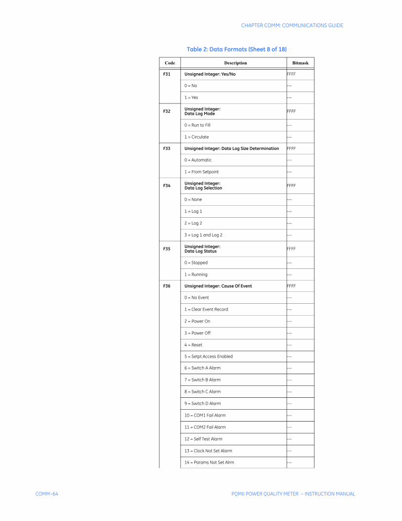
COMM–64 PQMII POWER QUALITY METER – INSTRUCTION MANUAL
CHAPTER COMM: COMMUNICATIONS GUIDE
F31 Unsigned Integer: Yes/No FFFF
0 = No ---
1 = Yes ---
F32 Unsigned Integer:Data Log Mode FFFF
0 = Run to Fill ---
1 = Circulate ---
F33 Unsigned Integer: Data Log Size Determination FFFF
0 = Automatic ---
1 = From Setpoint ---
F34 Unsigned Integer:Data Log Selection FFFF
0 = None ---
1 = Log 1 ---
2 = Log 2 ---
3 = Log 1 and Log 2 ---
F35 Unsigned Integer:Data Log Status FFFF
0 = Stopped ---
1 = Running ---
F36 Unsigned Integer: Cause Of Event FFFF
0 = No Event ---
1 = Clear Event Record ---
2 = Power On ---
3 = Power Off ---
4 = Reset ---
5 = Setpt Access Enabled ---
6 = Switch A Alarm ---
7 = Switch B Alarm ---
8 = Switch C Alarm ---
9 = Switch D Alarm ---
10 = COM1 Fail Alarm ---
11 = COM2 Fail Alarm ---
12 = Self Test Alarm ---
13 = Clock Not Set Alarm ---
14 = Params Not Set Alrm ---
Table 2: Data Formats (Sheet 8 of 18)
Code Description Bitmask
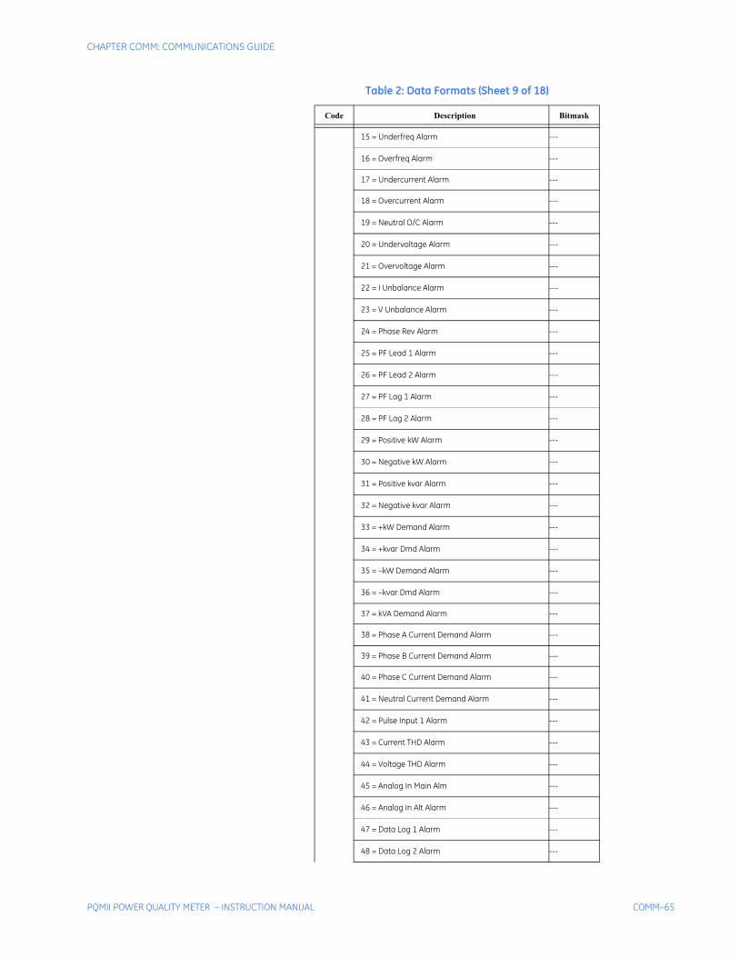
CHAPTER COMM: COMMUNICATIONS GUIDE
PQMII POWER QUALITY METER – INSTRUCTION MANUAL COMM–65
15 = Underfreq Alarm ---
16 = Overfreq Alarm ---
17 = Undercurrent Alarm ---
18 = Overcurrent Alarm ---
19 = Neutral O/C Alarm ---
20 = Undervoltage Alarm ---
21 = Overvoltage Alarm ---
22 = I Unbalance Alarm ---
23 = V Unbalance Alarm ---
24 = Phase Rev Alarm ---
25 = PF Lead 1 Alarm ---
26 = PF Lead 2 Alarm ---
27 = PF Lag 1 Alarm ---
28 = PF Lag 2 Alarm ---
29 = Positive kW Alarm ---
30 = Negative kW Alarm ---
31 = Positive kvar Alarm ---
32 = Negative kvar Alarm ---
33 = +kW Demand Alarm ---
34 = +kvar Dmd Alarm ---
35 = –kW Demand Alarm ---
36 = –kvar Dmd Alarm ---
37 = kVA Demand Alarm ---
38 = Phase A Current Demand Alarm ---
39 = Phase B Current Demand Alarm ---
40 = Phase C Current Demand Alarm ---
41 = Neutral Current Demand Alarm ---
42 = Pulse Input 1 Alarm ---
43 = Current THD Alarm ---
44 = Voltage THD Alarm ---
45 = Analog In Main Alm ---
46 = Analog In Alt Alarm ---
47 = Data Log 1 Alarm ---
48 = Data Log 2 Alarm ---
Table 2: Data Formats (Sheet 9 of 18)
Code Description Bitmask
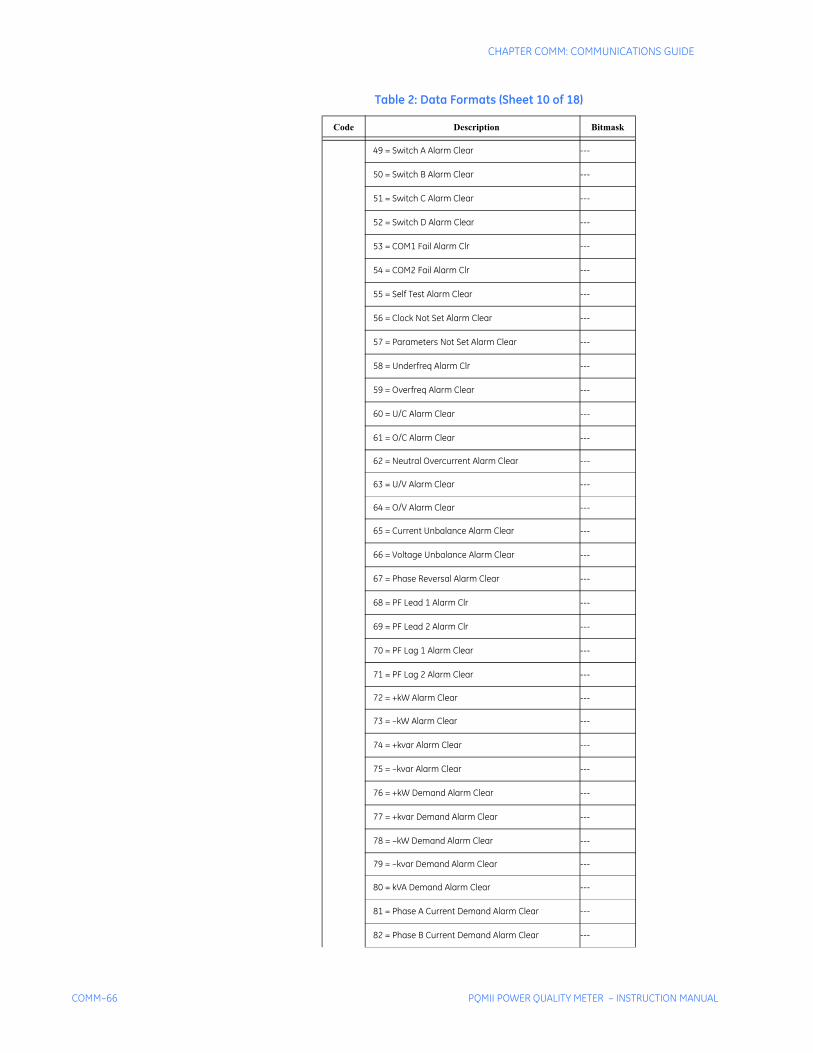
COMM–66 PQMII POWER QUALITY METER – INSTRUCTION MANUAL
CHAPTER COMM: COMMUNICATIONS GUIDE
49 = Switch A Alarm Clear ---
50 = Switch B Alarm Clear ---
51 = Switch C Alarm Clear ---
52 = Switch D Alarm Clear ---
53 = COM1 Fail Alarm Clr ---
54 = COM2 Fail Alarm Clr ---
55 = Self Test Alarm Clear ---
56 = Clock Not Set Alarm Clear ---
57 = Parameters Not Set Alarm Clear ---
58 = Underfreq Alarm Clr ---
59 = Overfreq Alarm Clear ---
60 = U/C Alarm Clear ---
61 = O/C Alarm Clear ---
62 = Neutral Overcurrent Alarm Clear ---
63 = U/V Alarm Clear ---
64 = O/V Alarm Clear ---
65 = Current Unbalance Alarm Clear ---
66 = Voltage Unbalance Alarm Clear ---
67 = Phase Reversal Alarm Clear ---
68 = PF Lead 1 Alarm Clr ---
69 = PF Lead 2 Alarm Clr ---
70 = PF Lag 1 Alarm Clear ---
71 = PF Lag 2 Alarm Clear ---
72 = +kW Alarm Clear ---
73 = –kW Alarm Clear ---
74 = +kvar Alarm Clear ---
75 = –kvar Alarm Clear ---
76 = +kW Demand Alarm Clear ---
77 = +kvar Demand Alarm Clear ---
78 = –kW Demand Alarm Clear ---
79 = –kvar Demand Alarm Clear ---
80 = kVA Demand Alarm Clear ---
81 = Phase A Current Demand Alarm Clear ---
82 = Phase B Current Demand Alarm Clear ---
Table 2: Data Formats (Sheet 10 of 18)
Code Description Bitmask
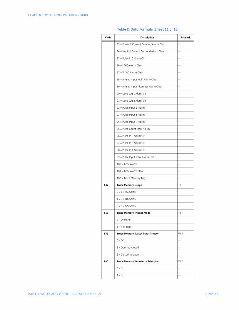
CHAPTER COMM: COMMUNICATIONS GUIDE
PQMII POWER QUALITY METER – INSTRUCTION MANUAL COMM–67
83 = Phase C Current Demand Alarm Clear ---
84 = Neutral Current Demand Alarm Clear ---
85 = Pulse In 1 Alarm Clr ---
86 = I THD Alarm Clear ---
87 = V THD Alarm Clear ---
88 = Analog Input Main Alarm Clear ---
89 = Analog Input Alternate Alarm Clear ---
90 = Data Log 1 Alarm Clr ---
91 = Data Log 2 Alarm Clr ---
92 = Pulse Input 2 Alarm ---
93 = Pulse Input 3 Alarm ---
94 = Pulse Input 4 Alarm ---
95 = Pulse Count Total Alarm ---
96 = Pulse In 2 Alarm Clr ---
97 = Pulse In 3 Alarm Clr ---
98 = Pulse In 4 Alarm Clr ---
99 = Pulse Input Total Alarm Clear ---
100 = Time Alarm ---
101 = Time Alarm Clear ---
102 = Trace Memory Trig ---
F37 Trace Memory Usage FFFF
0 = 1 x 36 cycles ---
1 = 2 x 18 cycles ---
2 = 3 x 12 cycles ---
F38 Trace Memory Trigger Mode FFFF
0 = One Shot ---
1 = Retrigger ---
F39 Trace Memory Switch Input Trigger FFFF
0 = Off ---
1 = Open-to-closed ---
2 = Closed-to-open ---
F40 Trace Memory Waveform Selection FFFF
0 = Ia ---
1 = Ib ---
Table 2: Data Formats (Sheet 11 of 18)
Code Description Bitmask
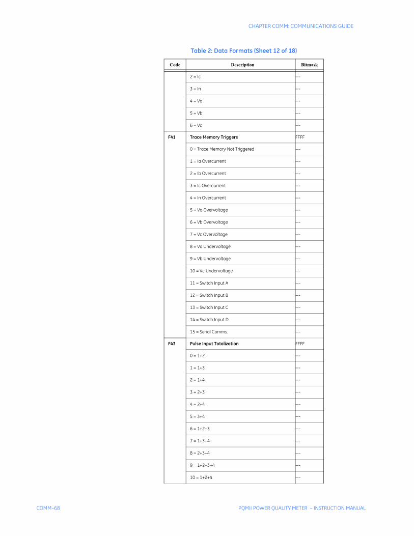
COMM–68 PQMII POWER QUALITY METER – INSTRUCTION MANUAL
CHAPTER COMM: COMMUNICATIONS GUIDE
2 = Ic ---
3 = In ---
4 = Va ---
5 = Vb ---
6 = Vc ---
F41 Trace Memory Triggers FFFF
0 = Trace Memory Not Triggered ---
1 = Ia Overcurrent ---
2 = Ib Overcurrent ---
3 = Ic Overcurrent ---
4 = In Overcurrent ---
5 = Va Overvoltage ---
6 = Vb Overvoltage ---
7 = Vc Overvoltage ---
8 = Va Undervoltage ---
9 = Vb Undervoltage ---
10 = Vc Undervoltage ---
11 = Switch Input A ---
12 = Switch Input B ---
13 = Switch Input C ---
14 = Switch Input D ---
15 = Serial Comms. ---
F43 Pulse Input Totalization FFFF
0 = 1+2 ---
1 = 1+3 ---
2 = 1+4 ---
3 = 2+3 ---
4 = 2+4 ---
5 = 3+4 ---
6 = 1+2+3 ---
7 = 1+3+4 ---
8 = 2+3+4 ---
9 = 1+2+3+4 ---
10 = 1+2+4 ---
Table 2: Data Formats (Sheet 12 of 18)
Code Description Bitmask
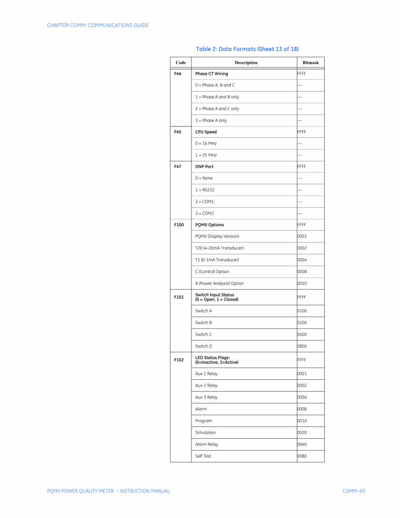
CHAPTER COMM: COMMUNICATIONS GUIDE
PQMII POWER QUALITY METER – INSTRUCTION MANUAL COMM–69
F44 Phase CT Wiring FFFF
0 = Phase A, B and C ---
1 = Phase A and B only ---
2 = Phase A and C only ---
3 = Phase A only ---
F45 CPU Speed FFFF
0 = 16 MHz ---
1 = 25 MHz ---
F47 DNP Port FFFF
0 = None ---
1 = RS232 ---
2 = COM1 ---
3 = COM2 ---
F100 PQMII Options FFFF
PQMII (Display Version) 0001
T20 (4-20mA Transducer) 0002
T1 (0-1mA Transducer) 0004
C (Control) Option 0008
A (Power Analysis) Option 0010
F101 Switch Input Status(0 = Open, 1 = Closed) FFFF
Switch A 0100
Switch B 0200
Switch C 0400
Switch D 0800
F102 LED Status Flags:(0=Inactive, 1=Active) FFFF
Aux 1 Relay 0001
Aux 2 Relay 0002
Aux 3 Relay 0004
Alarm 0008
Program 0010
Simulation 0020
Alarm Relay 0040
Self Test 0080
Table 2: Data Formats (Sheet 13 of 18)
Code Description Bitmask
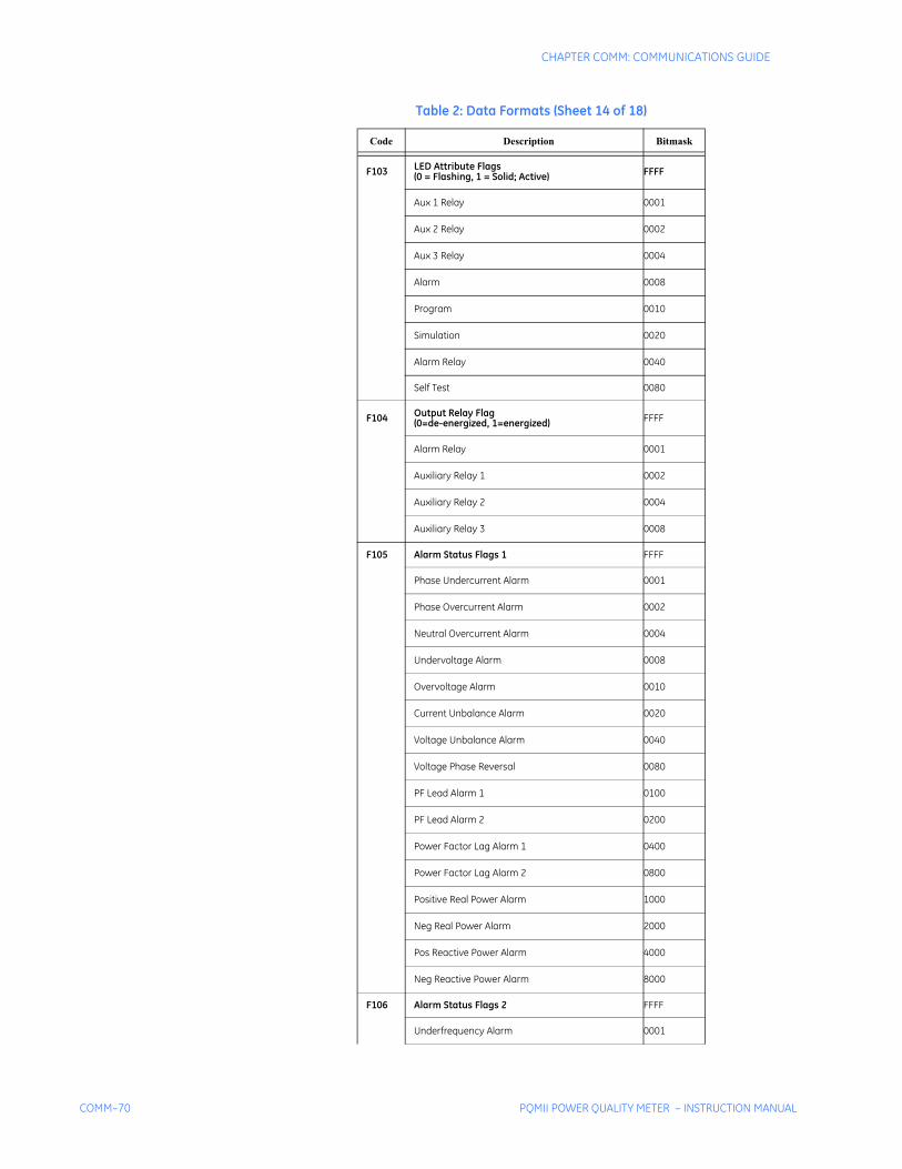
COMM–70 PQMII POWER QUALITY METER – INSTRUCTION MANUAL
CHAPTER COMM: COMMUNICATIONS GUIDE
F103 LED Attribute Flags(0 = Flashing, 1 = Solid; Active) FFFF
Aux 1 Relay 0001
Aux 2 Relay 0002
Aux 3 Relay 0004
Alarm 0008
Program 0010
Simulation 0020
Alarm Relay 0040
Self Test 0080
F104 Output Relay Flag(0=de-energized, 1=energized) FFFF
Alarm Relay 0001
Auxiliary Relay 1 0002
Auxiliary Relay 2 0004
Auxiliary Relay 3 0008
F105 Alarm Status Flags 1 FFFF
Phase Undercurrent Alarm 0001
Phase Overcurrent Alarm 0002
Neutral Overcurrent Alarm 0004
Undervoltage Alarm 0008
Overvoltage Alarm 0010
Current Unbalance Alarm 0020
Voltage Unbalance Alarm 0040
Voltage Phase Reversal 0080
PF Lead Alarm 1 0100
PF Lead Alarm 2 0200
Power Factor Lag Alarm 1 0400
Power Factor Lag Alarm 2 0800
Positive Real Power Alarm 1000
Neg Real Power Alarm 2000
Pos Reactive Power Alarm 4000
Neg Reactive Power Alarm 8000
F106 Alarm Status Flags 2 FFFF
Underfrequency Alarm 0001
Table 2: Data Formats (Sheet 14 of 18)
Code Description Bitmask
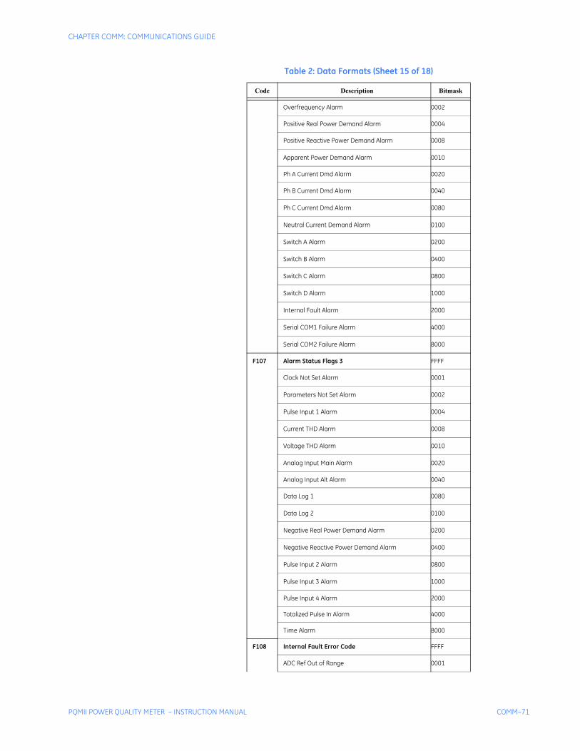
CHAPTER COMM: COMMUNICATIONS GUIDE
PQMII POWER QUALITY METER – INSTRUCTION MANUAL COMM–71
Overfrequency Alarm 0002
Positive Real Power Demand Alarm 0004
Positive Reactive Power Demand Alarm 0008
Apparent Power Demand Alarm 0010
Ph A Current Dmd Alarm 0020
Ph B Current Dmd Alarm 0040
Ph C Current Dmd Alarm 0080
Neutral Current Demand Alarm 0100
Switch A Alarm 0200
Switch B Alarm 0400
Switch C Alarm 0800
Switch D Alarm 1000
Internal Fault Alarm 2000
Serial COM1 Failure Alarm 4000
Serial COM2 Failure Alarm 8000
F107 Alarm Status Flags 3 FFFF
Clock Not Set Alarm 0001
Parameters Not Set Alarm 0002
Pulse Input 1 Alarm 0004
Current THD Alarm 0008
Voltage THD Alarm 0010
Analog Input Main Alarm 0020
Analog Input Alt Alarm 0040
Data Log 1 0080
Data Log 2 0100
Negative Real Power Demand Alarm 0200
Negative Reactive Power Demand Alarm 0400
Pulse Input 2 Alarm 0800
Pulse Input 3 Alarm 1000
Pulse Input 4 Alarm 2000
Totalized Pulse In Alarm 4000
Time Alarm 8000
F108 Internal Fault Error Code FFFF
ADC Ref Out of Range 0001
Table 2: Data Formats (Sheet 15 of 18)
Code Description Bitmask
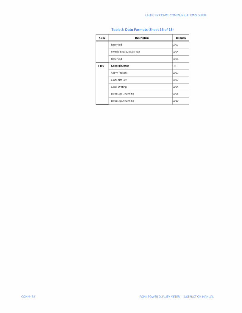
COMM–72 PQMII POWER QUALITY METER – INSTRUCTION MANUAL
CHAPTER COMM: COMMUNICATIONS GUIDE
Reserved 0002
Switch Input Circuit Fault 0004
Reserved 0008
F109 General Status FFFF
Alarm Present 0001
Clock Not Set 0002
Clock Drifting 0004
Data Log 1 Running 0008
Data Log 2 Running 0010
Table 2: Data Formats (Sheet 16 of 18)
Code Description Bitmask
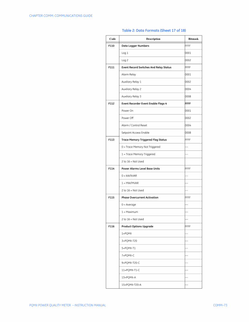
CHAPTER COMM: COMMUNICATIONS GUIDE
PQMII POWER QUALITY METER – INSTRUCTION MANUAL COMM–73
F110 Data Logger Numbers FFFF
Log 1 0001
Log 2 0002
F111 Event Record Switches And Relay Status FFFF
Alarm Relay 0001
Auxiliary Relay 1 0002
Auxiliary Relay 2 0004
Auxiliary Relay 3 0008
F112 Event Recorder Event Enable Flags 4 FFFF
Power On 0001
Power Off 0002
Alarm / Control Reset 0004
Setpoint Access Enable 0008
F113 Trace Memory Triggered Flag Status FFFF
0 = Trace Memory Not Triggered ---
1 = Trace Memory Triggered ---
2 to 16 = Not Used
F114 Power Alarms Level Base Units FFFF
0 = kW/kVAR ---
1 = MW/MVAR ---
2 to 16 = Not Used ---
F115 Phase Overcurrent Activation FFFF
0 = Average ---
1 = Maximum ---
2 to 16 = Not Used ---
F116 Product Options Upgrade FFFF
1=PQMII ---
3=PQMII-T20 ---
5=PQMII-T1 ---
7=PQMII-C ---
9=PQMII-T20-C ---
11=PQMII-T1-C ---
13=PQMII-A ---
15=PQMII-T20-A ---
Table 2: Data Formats (Sheet 17 of 18)
Code Description Bitmask
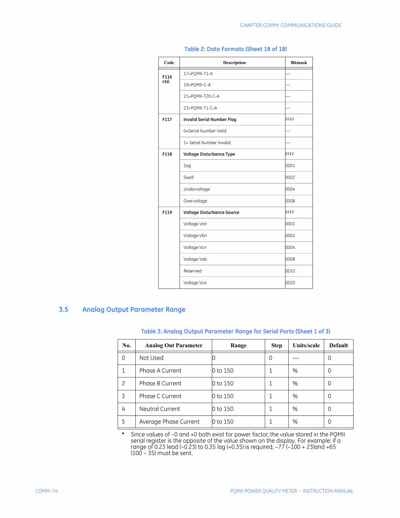
COMM–74 PQMII POWER QUALITY METER – INSTRUCTION MANUAL
CHAPTER COMM: COMMUNICATIONS GUIDE
3.5 Analog Output Parameter Range
F116 ctd.
17=PQMII-T1-A ---
19=PQMII-C-A ---
21=PQMII-T20-C-A ---
23=PQMII-T1-C-A ---
F117 Invalid Serial Number Flag FFFF
0=Serial Number Valid ---
1= Serial Number Invalid ---
F118 Voltage Disturbance Type FFFF
Sag 0001
Swell 0002
Undervoltage 0004
Overvoltage 0008
F119 Voltage Disturbance Source FFFF
Voltage Van 0001
Voltage Vbn 0002
Voltage Vcn 0004
Voltage Vab 0008
Reserved 0010
Voltage Vca 0020
Table 2: Data Formats (Sheet 18 of 18)
Code Description Bitmask
Table 3: Analog Output Parameter Range for Serial Ports (Sheet 1 of 3)
No. Analog Out Parameter Range Step Units/scale Default
0 Not Used 0 0 --- 0
1 Phase A Current 0 to 150 1 % 0
2 Phase B Current 0 to 150 1 % 0
3 Phase C Current 0 to 150 1 % 0
4 Neutral Current 0 to 150 1 % 0
5 Average Phase Current 0 to 150 1 % 0
* Since values of –0 and +0 both exist for power factor, the value stored in the PQMII serial register is the opposite of the value shown on the display. For example: if a range of 0.23 lead (–0.23) to 0.35 lag (+0.35) is required, –77 (–100 + 23)and +65 (100 – 35) must be sent.
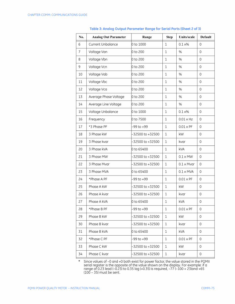
CHAPTER COMM: COMMUNICATIONS GUIDE
PQMII POWER QUALITY METER – INSTRUCTION MANUAL COMM–75
6 Current Unbalance 0 to 1000 1 0.1 x% 0
7 Voltage Van 0 to 200 1 % 0
8 Voltage Vbn 0 to 200 1 % 0
9 Voltage Vcn 0 to 200 1 % 0
10 Voltage Vab 0 to 200 1 % 0
11 Voltage Vbc 0 to 200 1 % 0
12 Voltage Vca 0 to 200 1 % 0
13 Average Phase Voltage 0 to 200 1 % 0
14 Average Line Voltage 0 to 200 1 % 0
15 Voltage Unbalance 0 to 1000 1 0.1 x% 0
16 Frequency 0 to 7500 1 0.01 x Hz 0
17 *3 Phase PF –99 to +99 1 0.01 x PF 0
18 3 Phase kW –32500 to +32500 1 kW 0
19 3 Phase kvar –32500 to +32500 1 kvar 0
20 3 Phase kVA 0 to 65400 1 kVA 0
21 3 Phase MW –32500 to +32500 1 0.1 x MW 0
22 3 Phase Mvar –32500 to +32500 1 0.1 x Mvar 0
23 3 Phase MVA 0 to 65400 1 0.1 x MVA 0
24 *Phase A PF –99 to +99 1 0.01 x PF 0
25 Phase A kW –32500 to +32500 1 kW 0
26 Phase A kvar –32500 to +32500 1 kvar 0
27 Phase A kVA 0 to 65400 1 kVA 0
28 *Phase B PF –99 to +99 1 0.01 x PF 0
29 Phase B kW –32500 to +32500 1 kW 0
30 Phase B kvar –32500 to +32500 1 kvar 0
31 Phase B kVA 0 to 65400 1 kVA 0
32 *Phase C PF –99 to +99 1 0.01 x PF 0
33 Phase C kW –32500 to +32500 1 kW 0
34 Phase C kvar –32500 to +32500 1 kvar 0
Table 3: Analog Output Parameter Range for Serial Ports (Sheet 2 of 3)
No. Analog Out Parameter Range Step Units/scale Default
* Since values of –0 and +0 both exist for power factor, the value stored in the PQMII serial register is the opposite of the value shown on the display. For example: if a range of 0.23 lead (–0.23) to 0.35 lag (+0.35) is required, –77 (–100 + 23)and +65 (100 – 35) must be sent.
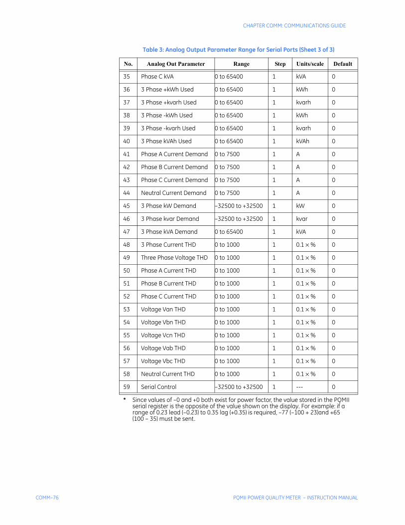
COMM–76 PQMII POWER QUALITY METER – INSTRUCTION MANUAL
CHAPTER COMM: COMMUNICATIONS GUIDE
35 Phase C kVA 0 to 65400 1 kVA 0
36 3 Phase +kWh Used 0 to 65400 1 kWh 0
37 3 Phase +kvarh Used 0 to 65400 1 kvarh 0
38 3 Phase -kWh Used 0 to 65400 1 kWh 0
39 3 Phase -kvarh Used 0 to 65400 1 kvarh 0
40 3 Phase kVAh Used 0 to 65400 1 kVAh 0
41 Phase A Current Demand 0 to 7500 1 A 0
42 Phase B Current Demand 0 to 7500 1 A 0
43 Phase C Current Demand 0 to 7500 1 A 0
44 Neutral Current Demand 0 to 7500 1 A 0
45 3 Phase kW Demand –32500 to +32500 1 kW 0
46 3 Phase kvar Demand –32500 to +32500 1 kvar 0
47 3 Phase kVA Demand 0 to 65400 1 kVA 0
48 3 Phase Current THD 0 to 1000 1 0.1 × % 0
49 Three Phase Voltage THD 0 to 1000 1 0.1 × % 0
50 Phase A Current THD 0 to 1000 1 0.1 × % 0
51 Phase B Current THD 0 to 1000 1 0.1 × % 0
52 Phase C Current THD 0 to 1000 1 0.1 × % 0
53 Voltage Van THD 0 to 1000 1 0.1 × % 0
54 Voltage Vbn THD 0 to 1000 1 0.1 × % 0
55 Voltage Vcn THD 0 to 1000 1 0.1 × % 0
56 Voltage Vab THD 0 to 1000 1 0.1 × % 0
57 Voltage Vbc THD 0 to 1000 1 0.1 × % 0
58 Neutral Current THD 0 to 1000 1 0.1 × % 0
59 Serial Control –32500 to +32500 1 --- 0
Table 3: Analog Output Parameter Range for Serial Ports (Sheet 3 of 3)
No. Analog Out Parameter Range Step Units/scale Default
* Since values of –0 and +0 both exist for power factor, the value stored in the PQMII serial register is the opposite of the value shown on the display. For example: if a range of 0.23 lead (–0.23) to 0.35 lag (+0.35) is required, –77 (–100 + 23)and +65 (100 – 35) must be sent.
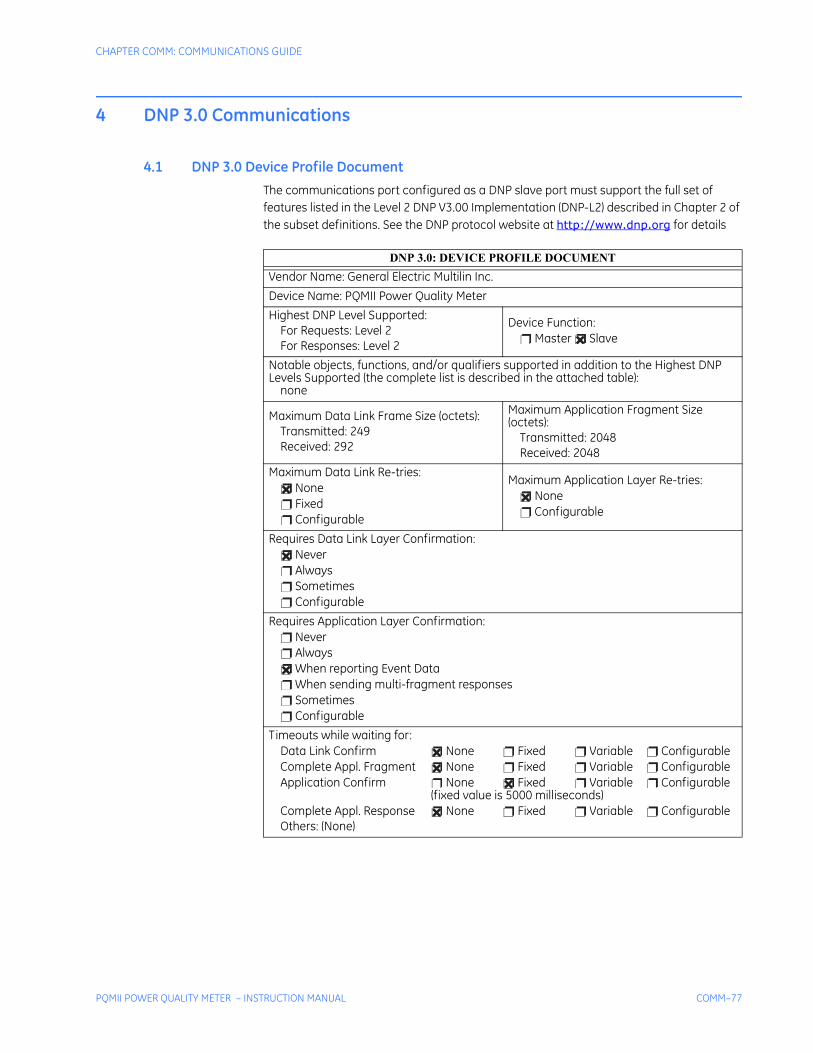
CHAPTER COMM: COMMUNICATIONS GUIDE
PQMII POWER QUALITY METER – INSTRUCTION MANUAL COMM–77
4 DNP 3.0 Communications
4.1 DNP 3.0 Device Profile DocumentThe communications port configured as a DNP slave port must support the full set of features listed in the Level 2 DNP V3.00 Implementation (DNP-L2) described in Chapter 2 of the subset definitions. See the DNP protocol website at http://www.dnp.org for details
DNP 3.0: DEVICE PROFILE DOCUMENT Vendor Name: General Electric Multilin Inc.Device Name: PQMII Power Quality MeterHighest DNP Level Supported:
For Requests: Level 2For Responses: Level 2
Device Function: Master Slave
Notable objects, functions, and/or qualifiers supported in addition to the Highest DNP Levels Supported (the complete list is described in the attached table):
none
Maximum Data Link Frame Size (octets):Transmitted: 249Received: 292
Maximum Application Fragment Size (octets):
Transmitted: 2048Received: 2048
Maximum Data Link Re-tries: None Fixed Configurable
Maximum Application Layer Re-tries: None Configurable
Requires Data Link Layer Confirmation: Never Always Sometimes Configurable
Requires Application Layer Confirmation: Never Always When reporting Event Data When sending multi-fragment responses Sometimes Configurable
Timeouts while waiting for:Data Link Confirm None Fixed Variable ConfigurableComplete Appl. Fragment None Fixed Variable ConfigurableApplication Confirm None Fixed Variable Configurable
(fixed value is 5000 milliseconds)Complete Appl. Response None Fixed Variable ConfigurableOthers: (None)
� ��
��
�
�
��
�
��
�
�
�
�
�
��
�
�
�
�� � � �
�� � � �
� �� � �
�� � � �
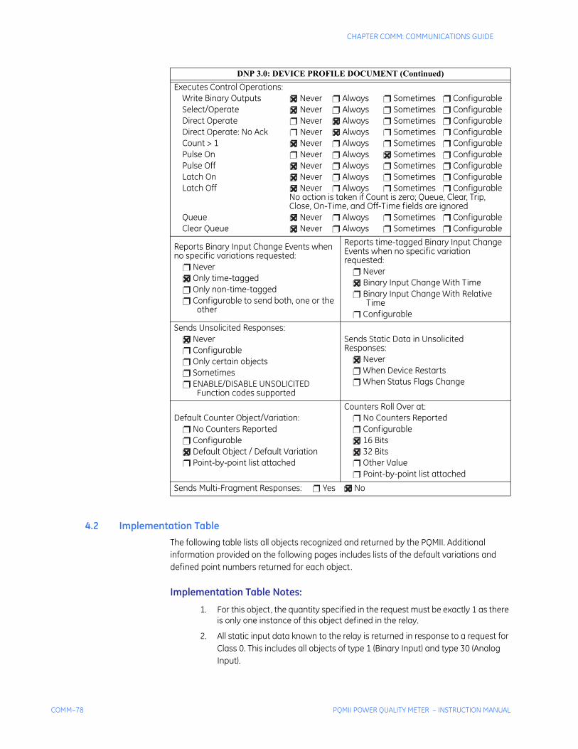
COMM–78 PQMII POWER QUALITY METER – INSTRUCTION MANUAL
CHAPTER COMM: COMMUNICATIONS GUIDE
4.2 Implementation TableThe following table lists all objects recognized and returned by the PQMII. Additional information provided on the following pages includes lists of the default variations and defined point numbers returned for each object.
Implementation Table Notes:
1. For this object, the quantity specified in the request must be exactly 1 as there is only one instance of this object defined in the relay.
2. All static input data known to the relay is returned in response to a request for Class 0. This includes all objects of type 1 (Binary Input) and type 30 (Analog Input).
Executes Control Operations:Write Binary Outputs Never Always Sometimes ConfigurableSelect/Operate Never Always Sometimes ConfigurableDirect Operate Never Always Sometimes ConfigurableDirect Operate: No Ack Never Always Sometimes ConfigurableCount > 1 Never Always Sometimes ConfigurablePulse On Never Always Sometimes ConfigurablePulse Off Never Always Sometimes ConfigurableLatch On Never Always Sometimes ConfigurableLatch Off Never Always Sometimes Configurable
No action is taken if Count is zero; Queue, Clear, Trip, Close, On-Time, and Off-Time fields are ignored
Queue Never Always Sometimes ConfigurableClear Queue Never Always Sometimes Configurable
Reports Binary Input Change Events when no specific variations requested:
Never Only time-tagged Only non-time-tagged Configurable to send both, one or the
other
Reports time-tagged Binary Input Change Events when no specific variation requested:
Never Binary Input Change With Time Binary Input Change With Relative
Time Configurable
Sends Unsolicited Responses: Never Configurable Only certain objects Sometimes ENABLE/DISABLE UNSOLICITED
Function codes supported
Sends Static Data in Unsolicited Responses:
Never When Device Restarts When Status Flags Change
Default Counter Object/Variation: No Counters Reported Configurable Default Object / Default Variation Point-by-point list attached
Counters Roll Over at: No Counters Reported Configurable 16 Bits 32 Bits Other Value Point-by-point list attached
Sends Multi-Fragment Responses: Yes No
DNP 3.0: DEVICE PROFILE DOCUMENT (Continued)
�� � � �
�� � � �
� �� � �
� �� � �
�� � � �
� � �� �
�� � � �
�� � � �
�� � � �
�� � � �
�� � � �
�
��
�
�
�
��
�
�
��
�
�
�
�
��
�
�
�
�
��
�
�
�
��
��
�
�
� ��
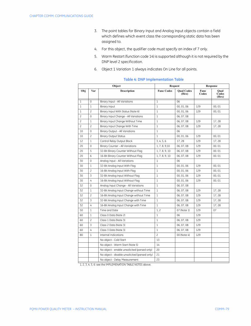
CHAPTER COMM: COMMUNICATIONS GUIDE
PQMII POWER QUALITY METER – INSTRUCTION MANUAL COMM–79
3. The point tables for Binary Input and Analog Input objects contain a field which defines which event class the corresponding static data has been assigned to.
4. For this object, the qualifier code must specify an index of 7 only.
5. Warm Restart (function code 14) is supported although it is not required by the DNP level 2 specification.
6. Object 1 Variation 1 always indicates On Line for all points.
Table 4: DNP Implementation Table
Object Request Response
Obj Var Description Func Codes Qual Codes (Hex)
Func Codes
Qual Codes (Hex)
1 0 Binary Input - All Variations 1 06
1 1 Binary Input 1 00, 01, 06 129 00, 01
1 2 Binary Input With Status (Note 6) 1 00, 01, 06 129 00, 01
2 0 Binary Input Change - All Variations 1 06, 07, 08
2 1 Binary Input Change Without Time 1 06, 07, 08 129 17, 28
2 2 Binary Input Change With Time 1 06, 07, 08 129 17, 28
10 0 Binary Output - All Variations 1 06
10 2 Binary Output Status 1 00, 01, 06 129 00, 01
12 1 Control Relay Output Block 3, 4, 5, 6 17, 28 129 17, 28
20 0 Binary Counter - All Variations 1, 7, 8, 9,10 06, 07, 08 129 00. 01
20 5 32-Bit Binary Counter Without Flag 1, 7, 8, 9, 10 06, 07, 08 129 00. 01
20 6 16-Bit Binary Counter Without Flag 1, 7, 8, 9, 10 06, 07, 08 129 00. 01
30 0 Analog Input - All Variations 1 06
30 1 32-Bit Analog Input With Flag 1 00, 01, 06 129 00, 01
30 2 16-Bit Analog Input With Flag 1 00, 01, 06 129 00, 01
30 3 32-Bit Analog Input Without Flag 1 00, 01, 06 129 00, 01
30 4 16-Bit Analog Input Without Flag 1 00, 01, 06 129 00, 01
32 0 Analog Input Change - All Variations 1 06, 07, 08
32 1 32-Bit Analog Input Change without Time 1 06, 07, 08 129 17, 28
32 2 16-Bit Analog Input Change without Time 1 06, 07, 08 129 17, 28
32 3 32-Bit Analog Input Change with Time 1 06, 07, 08 129 17, 28
32 4 16-Bit Analog Input Change with Time 1 06, 07, 08 129 17, 28
50 1 Time and Date 1, 2 07 (Note 1) 129 07
60 1 Class 0 Data (Note 2) 1 06 129
60 2 Class 1 Data (Note 3) 1 06, 07, 08 129
60 3 Class 2 Data (Note 3) 1 06, 07, 08 129
60 4 Class 3 Data (Note 3) 1 06, 07, 08 129
80 1 Internal Indications 2 00 (Note 4) 129
No object - Cold Start 13
No object - Warm Start (Note 5) 14
No object - enable unsolicited (parsed only) 20
No object - disable unsolicited (parsed only) 21
No object - Delay Measurement 23
1, 2, 3, 4, 5, 6: see the IMPLEMENATION TABLE NOTES above.
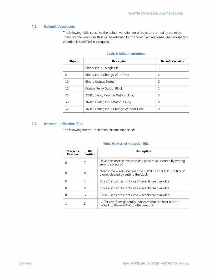
COMM–80 PQMII POWER QUALITY METER – INSTRUCTION MANUAL
CHAPTER COMM: COMMUNICATIONS GUIDE
4.3 Default VariationsThe following table specifies the default variation for all objects returned by the relay. These are the variations that will be returned for the object in a response when no specific variation is specified in a request.
4.4 Internal Indication BitsThe following internal indication bits are supported:
Table 5: Default Variations
Object Description Default Variation
1 Binary Input - Single Bit 1
2 Binary Input Change With Time 2
10 Binary Output Status 2
12 Control Relay Output Block 1
20 32-Bit Binary Counter Without Flag 5
30 16-Bit Analog Input Without Flag 2
32 16-Bit Analog Input Change Without Time 2
Table 6: Internal Indication Bits
Character Position
Bit Position
Description
0 7 Device Restart: set when PQMII powers up, cleared by writing zero to object 80
0 4 Need Time -- set whenever the PQMII has a “CLOCK NOT SET” alarm, cleared by setting the clock
0 1 Class 1: indicates that class 1 events are available
0 2 Class 2: indicates that class 2 events are available
0 3 Class 3: indicates that class 2 events are available
1 3 Buffer Overflow: generally indicates that the host has not picked up the event data often enough
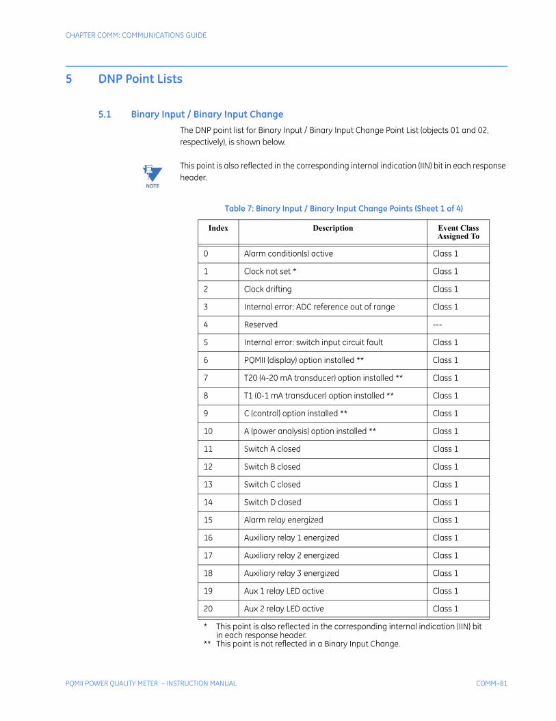
CHAPTER COMM: COMMUNICATIONS GUIDE
PQMII POWER QUALITY METER – INSTRUCTION MANUAL COMM–81
5 DNP Point Lists
5.1 Binary Input / Binary Input ChangeThe DNP point list for Binary Input / Binary Input Change Point List (objects 01 and 02, respectively), is shown below.
Note This point is also reflected in the corresponding internal indication (IIN) bit in each response header.
Table 7: Binary Input / Binary Input Change Points (Sheet 1 of 4)
Index Description Event Class Assigned To
0 Alarm condition(s) active Class 1
1 Clock not set * Class 1
2 Clock drifting Class 1
3 Internal error: ADC reference out of range Class 1
4 Reserved ---
5 Internal error: switch input circuit fault Class 1
6 PQMII (display) option installed ** Class 1
7 T20 (4-20 mA transducer) option installed ** Class 1
8 T1 (0-1 mA transducer) option installed ** Class 1
9 C (control) option installed ** Class 1
10 A (power analysis) option installed ** Class 1
11 Switch A closed Class 1
12 Switch B closed Class 1
13 Switch C closed Class 1
14 Switch D closed Class 1
15 Alarm relay energized Class 1
16 Auxiliary relay 1 energized Class 1
17 Auxiliary relay 2 energized Class 1
18 Auxiliary relay 3 energized Class 1
19 Aux 1 relay LED active Class 1
20 Aux 2 relay LED active Class 1
* This point is also reflected in the corresponding internal indication (IIN) bit in each response header.
** This point is not reflected in a Binary Input Change.
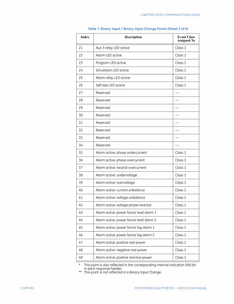
COMM–82 PQMII POWER QUALITY METER – INSTRUCTION MANUAL
CHAPTER COMM: COMMUNICATIONS GUIDE
21 Aux 3 relay LED active Class 1
22 Alarm LED active Class 1
23 Program LED active Class 1
24 Simulation LED active Class 1
25 Alarm relay LED active Class 1
26 Self test LED active Class 1
27 Reserved ---
28 Reserved ---
29 Reserved ---
30 Reserved ---
31 Reserved ---
32 Reserved ---
33 Reserved ---
34 Reserved ---
35 Alarm active: phase undercurrent Class 1
36 Alarm active: phase overcurrent Class 1
37 Alarm active: neutral overcurrent Class 1
38 Alarm active: undervoltage Class 1
39 Alarm active: overvoltage Class 1
40 Alarm active: current unbalance Class 1
41 Alarm active: voltage unbalance Class 1
42 Alarm active: voltage phase reversal Class 1
43 Alarm active: power factor lead alarm 1 Class 1
44 Alarm active: power factor lead alarm 2 Class 1
45 Alarm active: power factor lag alarm 1 Class 1
46 Alarm active: power factor lag alarm 2 Class 1
47 Alarm active: positive real power Class 1
48 Alarm active: negative real power Class 1
49 Alarm active: positive reactive power Class 1
Table 7: Binary Input / Binary Input Change Points (Sheet 2 of 4)
Index Description Event Class Assigned To
* This point is also reflected in the corresponding internal indication (IIN) bit in each response header.
** This point is not reflected in a Binary Input Change.
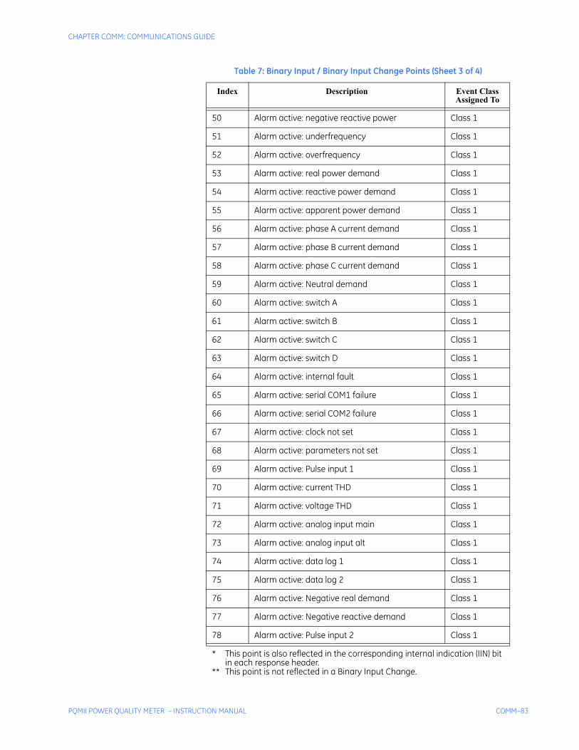
CHAPTER COMM: COMMUNICATIONS GUIDE
PQMII POWER QUALITY METER – INSTRUCTION MANUAL COMM–83
50 Alarm active: negative reactive power Class 1
51 Alarm active: underfrequency Class 1
52 Alarm active: overfrequency Class 1
53 Alarm active: real power demand Class 1
54 Alarm active: reactive power demand Class 1
55 Alarm active: apparent power demand Class 1
56 Alarm active: phase A current demand Class 1
57 Alarm active: phase B current demand Class 1
58 Alarm active: phase C current demand Class 1
59 Alarm active: Neutral demand Class 1
60 Alarm active: switch A Class 1
61 Alarm active: switch B Class 1
62 Alarm active: switch C Class 1
63 Alarm active: switch D Class 1
64 Alarm active: internal fault Class 1
65 Alarm active: serial COM1 failure Class 1
66 Alarm active: serial COM2 failure Class 1
67 Alarm active: clock not set Class 1
68 Alarm active: parameters not set Class 1
69 Alarm active: Pulse input 1 Class 1
70 Alarm active: current THD Class 1
71 Alarm active: voltage THD Class 1
72 Alarm active: analog input main Class 1
73 Alarm active: analog input alt Class 1
74 Alarm active: data log 1 Class 1
75 Alarm active: data log 2 Class 1
76 Alarm active: Negative real demand Class 1
77 Alarm active: Negative reactive demand Class 1
78 Alarm active: Pulse input 2 Class 1
Table 7: Binary Input / Binary Input Change Points (Sheet 3 of 4)
Index Description Event Class Assigned To
* This point is also reflected in the corresponding internal indication (IIN) bit in each response header.
** This point is not reflected in a Binary Input Change.
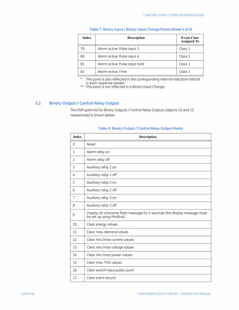
COMM–84 PQMII POWER QUALITY METER – INSTRUCTION MANUAL
CHAPTER COMM: COMMUNICATIONS GUIDE
5.2 Binary Output / Control Relay OutputThe DNP point list for Binary Outputs / Control Relay Outputs (objects 10 and 12, respectively) is shown below:
79 Alarm active: Pulse input 3 Class 1
80 Alarm active: Pulse input 4 Class 1
81 Alarm active: Pulse input total Class 1
82 Alarm active: Time Class 1
Table 7: Binary Input / Binary Input Change Points (Sheet 4 of 4)
Index Description Event Class Assigned To
* This point is also reflected in the corresponding internal indication (IIN) bit in each response header.
** This point is not reflected in a Binary Input Change.
Table 8: Binary Output / Control Relay Output Points
Index Description
0 Reset
1 Alarm relay on
2 Alarm relay off
3 Auxiliary relay 1 on
4 Auxiliary relay 1 off
5 Auxiliary relay 2 on
6 Auxiliary relay 2 off
7 Auxiliary relay 3 on
8 Auxiliary relay 3 off
9 Display 40 character flash message for 5 seconds (the display message must be set up using Modbus)
10 Clear energy values
11 Clear max. demand values
12 Clear min./max current values
13 Clear min./max voltage values
14 Clear min./max power values
15 Clear max. THD values
16 Clear switch input pulse count
17 Clear event record
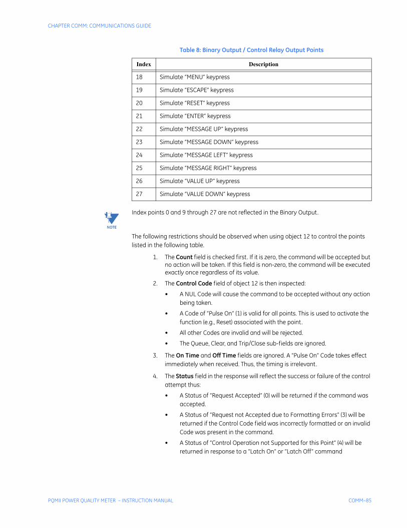
CHAPTER COMM: COMMUNICATIONS GUIDE
PQMII POWER QUALITY METER – INSTRUCTION MANUAL COMM–85
Note Index points 0 and 9 through 27 are not reflected in the Binary Output.
The following restrictions should be observed when using object 12 to control the points listed in the following table.
1. The Count field is checked first. If it is zero, the command will be accepted but no action will be taken. If this field is non-zero, the command will be executed exactly once regardless of its value.
2. The Control Code field of object 12 is then inspected:
• A NUL Code will cause the command to be accepted without any action being taken.
• A Code of “Pulse On” (1) is valid for all points. This is used to activate the function (e.g., Reset) associated with the point.
• All other Codes are invalid and will be rejected.
• The Queue, Clear, and Trip/Close sub-fields are ignored.
3. The On Time and Off Time fields are ignored. A “Pulse On” Code takes effect immediately when received. Thus, the timing is irrelevant.
4. The Status field in the response will reflect the success or failure of the control attempt thus:
• A Status of “Request Accepted” (0) will be returned if the command was accepted.
• A Status of “Request not Accepted due to Formatting Errors” (3) will be returned if the Control Code field was incorrectly formatted or an invalid Code was present in the command.
• A Status of “Control Operation not Supported for this Point” (4) will be returned in response to a “Latch On” or “Latch Off” command
18 Simulate “MENU” keypress
19 Simulate “ESCAPE” keypress
20 Simulate “RESET” keypress
21 Simulate “ENTER” keypress
22 Simulate “MESSAGE UP” keypress
23 Simulate “MESSAGE DOWN” keypress
24 Simulate “MESSAGE LEFT” keypress
25 Simulate “MESSAGE RIGHT” keypress
26 Simulate “VALUE UP” keypress
27 Simulate “VALUE DOWN” keypress
Table 8: Binary Output / Control Relay Output Points
Index Description
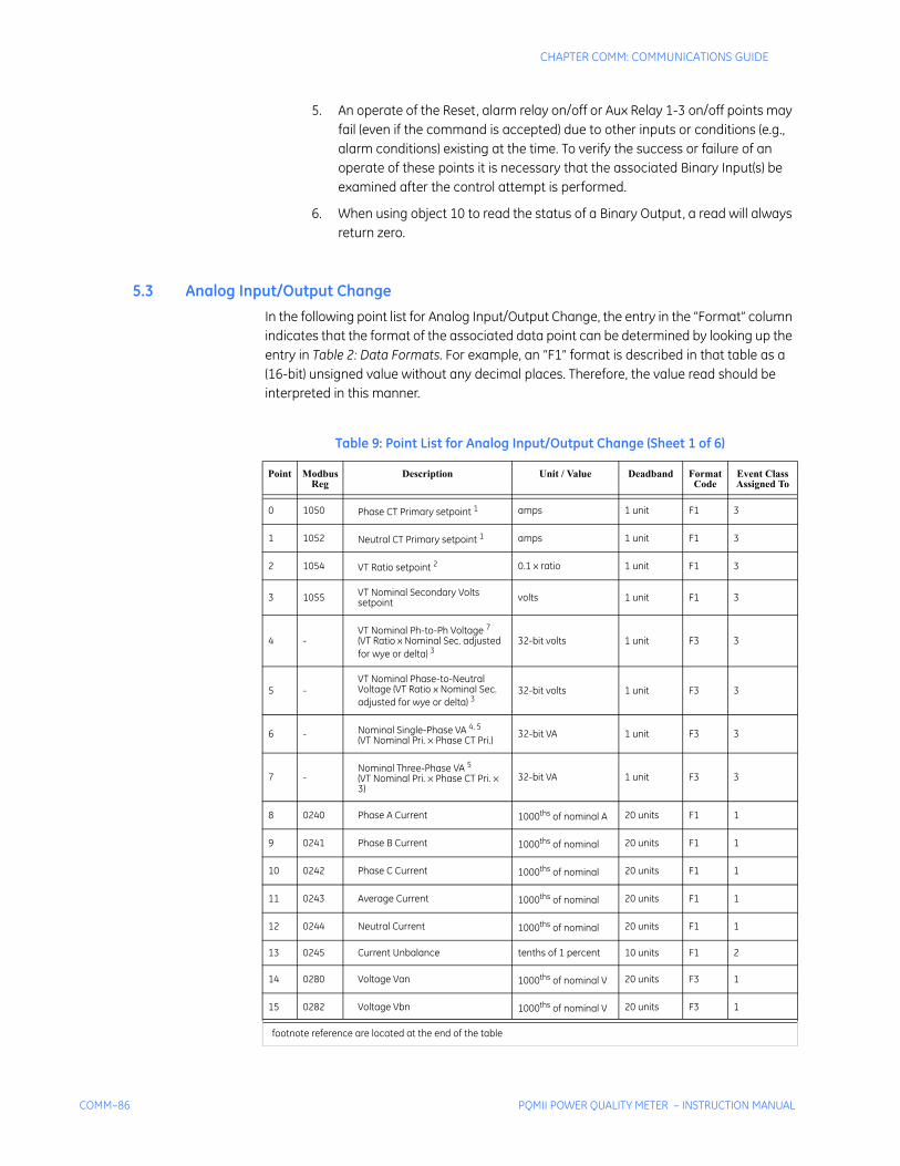
COMM–86 PQMII POWER QUALITY METER – INSTRUCTION MANUAL
CHAPTER COMM: COMMUNICATIONS GUIDE
5. An operate of the Reset, alarm relay on/off or Aux Relay 1-3 on/off points may fail (even if the command is accepted) due to other inputs or conditions (e.g., alarm conditions) existing at the time. To verify the success or failure of an operate of these points it is necessary that the associated Binary Input(s) be examined after the control attempt is performed.
6. When using object 10 to read the status of a Binary Output, a read will always return zero.
5.3 Analog Input/Output ChangeIn the following point list for Analog Input/Output Change, the entry in the “Format” column indicates that the format of the associated data point can be determined by looking up the entry in Table 2: Data Formats. For example, an “F1” format is described in that table as a (16-bit) unsigned value without any decimal places. Therefore, the value read should be interpreted in this manner.
Table 9: Point List for Analog Input/Output Change (Sheet 1 of 6)
Point Modbus Reg
Description Unit / Value Deadband Format Code
Event Class Assigned To
0 1050 Phase CT Primary setpoint 1 amps 1 unit F1 3
1 1052 Neutral CT Primary setpoint 1 amps 1 unit F1 3
2 1054 VT Ratio setpoint 2 0.1 x ratio 1 unit F1 3
3 1055 VT Nominal Secondary Volts setpoint volts 1 unit F1 3
4 -VT Nominal Ph-to-Ph Voltage 7(VT Ratio x Nominal Sec. adjusted for wye or delta) 3
32-bit volts 1 unit F3 3
5 -VT Nominal Phase-to-Neutral Voltage (VT Ratio x Nominal Sec. adjusted for wye or delta) 3
32-bit volts 1 unit F3 3
6 - Nominal Single-Phase VA 4, 5
(VT Nominal Pri. × Phase CT Pri.)32-bit VA 1 unit F3 3
7 -Nominal Three-Phase VA 5(VT Nominal Pri. × Phase CT Pri. × 3)
32-bit VA 1 unit F3 3
8 0240 Phase A Current 1000ths of nominal A 20 units F1 1
9 0241 Phase B Current 1000ths of nominal 20 units F1 1
10 0242 Phase C Current 1000ths of nominal 20 units F1 1
11 0243 Average Current 1000ths of nominal 20 units F1 1
12 0244 Neutral Current 1000ths of nominal 20 units F1 1
13 0245 Current Unbalance tenths of 1 percent 10 units F1 2
14 0280 Voltage Van 1000ths of nominal V 20 units F3 1
15 0282 Voltage Vbn 1000ths of nominal V 20 units F3 1
footnote reference are located at the end of the table
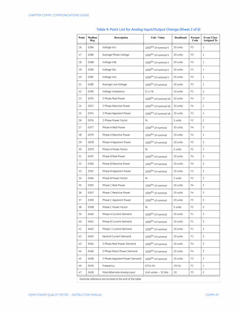
CHAPTER COMM: COMMUNICATIONS GUIDE
PQMII POWER QUALITY METER – INSTRUCTION MANUAL COMM–87
16 0284 Voltage Vcn 1000ths of nominal V 20 units F3 1
17 0286 Average Phase Voltage 1000ths of nominal V 20 units F3 1
18 0288 Voltage Vab 1000ths of nominal V 20 units F3 1
19 028A Voltage Vbc 1000ths of nominal V 20 units F3 1
20 028C Voltage Vca 1000ths of nominal V 20 units F3 1
21 028E Average Line Voltage 1000ths of nominal 20 units F3 1
22 0290 Voltage Unbalance 0.1 x % 10 units F1 2
23 02F0 3 Phase Real Power 1000ths of nominal VA 20 units F4 2
24 02F2 3 Phase Reactive Power 1000ths of nominal VA 20 units F4 2
25 02F4 3 Phase Apparent Power 1000ths of nominal VA 20 units F3 2
26 02F6 3 Phase Power Factor % 5 units F2 2
27 02F7 Phase A Real Power 1000ths of nominal 20 units F4 3
28 02F9 Phase A Reactive Power 1000ths of nominal 20 units F4 3
29 02FB Phase A Apparent Power 1000ths of nominal 20 units F3 3
30 02FD Phase A Power Factor % 5 units F2 3
31 02FE Phase B Real Power 1000ths of nominal 20 units F4 3
32 0300 Phase B Reactive Power 1000ths of nominal 20 units F4 3
33 0302 Phase B Apparent Power 1000ths of nominal 20 units F3 3
34 0304 Phase B Power Factor % 5 units F2 3
35 0305 Phase C Real Power 1000ths of nominal 20 units F4 3
36 0307 Phase C Reactive Power 1000ths of nominal 20 units F4 3
37 0309 Phase C Apparent Power 1000ths of nominal 20 units F3 3
38 030B Phase C Power Factor % 5 units F2 3
39 0400 Phase A Current Demand 1000ths of nominal 20 units F1 3
40 0401 Phase B Current Demand 1000ths of nominal 20 units F1 3
41 0402 Phase C Current Demand 1000ths of nominal 20 units F1 3
42 0403 Neutral Current Demand 1000ths of nominal 20 units F1 3
43 0404 3 Phase Real Power Demand 1000ths of nominal 20 units F4 3
44 0406 3 Phase React Power Demand 1000ths of nominal 20 units F4 3
45 0408 3 Phase Apparent Power Demand 1000ths of nominal 20 units F3 3
46 0440 Frequency 0.01x Hz .05 Hz F1 1
47 0458 Main/Alternate Analog Input Unit varies -- 32 bits 10 F3 2
Table 9: Point List for Analog Input/Output Change (Sheet 2 of 6)
Point Modbus Reg
Description Unit / Value Deadband Format Code
Event Class Assigned To
footnote reference are located at the end of the table
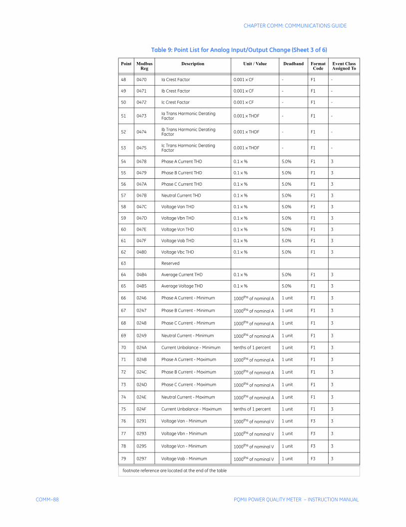
COMM–88 PQMII POWER QUALITY METER – INSTRUCTION MANUAL
CHAPTER COMM: COMMUNICATIONS GUIDE
48 0470 Ia Crest Factor 0.001 x CF - F1 -
49 0471 Ib Crest Factor 0.001 x CF - F1 -
50 0472 Ic Crest Factor 0.001 x CF - F1 -
51 0473 Ia Trans Harmonic Derating Factor 0.001 x THDF - F1 -
52 0474 Ib Trans Harmonic Derating Factor 0.001 x THDF - F1 -
53 0475 Ic Trans Harmonic Derating Factor 0.001 x THDF - F1 -
54 0478 Phase A Current THD 0.1 x % 5.0% F1 3
55 0479 Phase B Current THD 0.1 x % 5.0% F1 3
56 047A Phase C Current THD 0.1 x % 5.0% F1 3
57 047B Neutral Current THD 0.1 x % 5.0% F1 3
58 047C Voltage Van THD 0.1 x % 5.0% F1 3
59 047D Voltage Vbn THD 0.1 x % 5.0% F1 3
60 047E Voltage Vcn THD 0.1 x % 5.0% F1 3
61 047F Voltage Vab THD 0.1 x % 5.0% F1 3
62 0480 Voltage Vbc THD 0.1 x % 5.0% F1 3
63 Reserved
64 04B4 Average Current THD 0.1 x % 5.0% F1 3
65 04B5 Average Voltage THD 0.1 x % 5.0% F1 3
66 0246 Phase A Current - Minimum 1000ths of nominal A 1 unit F1 3
67 0247 Phase B Current - Minimum 1000ths of nominal A 1 unit F1 3
68 0248 Phase C Current - Minimum 1000ths of nominal A 1 unit F1 3
69 0249 Neutral Current - Minimum 1000ths of nominal A 1 unit F1 3
70 024A Current Unbalance - Minimum tenths of 1 percent 1 unit F1 3
71 024B Phase A Current - Maximum 1000ths of nominal A 1 unit F1 3
72 024C Phase B Current - Maximum 1000ths of nominal A 1 unit F1 3
73 024D Phase C Current - Maximum 1000ths of nominal A 1 unit F1 3
74 024E Neutral Current - Maximum 1000ths of nominal A 1 unit F1 3
75 024F Current Unbalance - Maximum tenths of 1 percent 1 unit F1 3
76 0291 Voltage Van - Minimum 1000ths of nominal V 1 unit F3 3
77 0293 Voltage Vbn - Minimum 1000ths of nominal V 1 unit F3 3
78 0295 Voltage Vcn - Minimum 1000ths of nominal V 1 unit F3 3
79 0297 Voltage Vab - Minimum 1000ths of nominal V 1 unit F3 3
Table 9: Point List for Analog Input/Output Change (Sheet 3 of 6)
Point Modbus Reg
Description Unit / Value Deadband Format Code
Event Class Assigned To
footnote reference are located at the end of the table
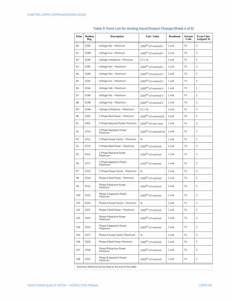
CHAPTER COMM: COMMUNICATIONS GUIDE
PQMII POWER QUALITY METER – INSTRUCTION MANUAL COMM–89
80 0299 Voltage Vbc - Minimum 1000ths of nominal V 1 unit F3 3
81 029B Voltage Vca - Minimum 1000ths of nominal V 1 unit F3 3
82 029D Voltage Unbalance - Minimum 0.1 x % 1 unit F1 3
83 029E Voltage Van - Maximum 1000ths of nominal V 1 unit F3 3
84 02A0 Voltage Vbn - Maximum 1000ths of nominal V 1 unit F3 3
85 02A2 Voltage Vcn - Maximum 1000ths of nominal V 1 unit F3 3
86 02A4 Voltage Vab - Maximum 1000ths of nominal V 1 unit F3 3
87 02A6 Voltage Vbc - Maximum 1000ths of nominal V 1 unit F3 3
88 02A8 Voltage Vca - Maximum 1000ths of nominal V 1 unit F3 3
89 02AA Voltage Unbalance - Maximum 0.1 x % 1 unit F1 3
90 030C 3 Phase Real Power - Minimum 1000ths of nominal W 1 unit F4 3
91 030E 3 Phase Reactive Power Minimum 1000ths of nom. kvar 1 unit F4 3
92 0310 3 Phase Apparent Power Minimum 1000ths of nominal VA 1 unit F3 3
93 0312 3 Phase Power Factor - Minimum % 1 unit F2 3
94 0313 3 Phase Real Power - Maximum 1000ths of nominal 1 unit F4 3
95 0315 3 Phase Reactive Power Maximum 1000ths of nominal 1 unit F4 3
96 0317 3 Phase Apparent Power Maximum 1000ths of nominal 1 unit F3 3
97 0319 3 Phase Power Factor - Maximum % 1 unit F2 3
98 031A Phase A Real Power - Minimum 1000ths of nominal 1 unit F4 3
99 031C Phase A Reactive Power Minimum 1000ths of nominal 1 unit F4 3
100 031E Phase A Apparent Power Minimum 1000ths of nominal 1 unit F3 3
101 0220 Phase A Power Factor - Minimum % 1 unit F2 3
102 0321 Phase A Real Power - Maximum 1000ths of nominal 1 unit F4 3
103 0323 Phase A Reactive Power Maximum 1000ths of nominal 1 unit F4 3
104 0325 Phase A Apparent Power Maximum 1000ths of nominal 1 unit F3 3
105 0327 Phase A Power Factor Maximum % 1 unit F2 3
106 0328 Phase B Real Power Minimum 1000ths of nominal 1 unit F4 3
107 032A Phase B Reactive Power Minimum 1000ths of nominal 1 unit F4 3
108 032C Phase B Apparent Power Minimum 1000ths of nominal 1 unit F3 3
Table 9: Point List for Analog Input/Output Change (Sheet 4 of 6)
Point Modbus Reg
Description Unit / Value Deadband Format Code
Event Class Assigned To
footnote reference are located at the end of the table
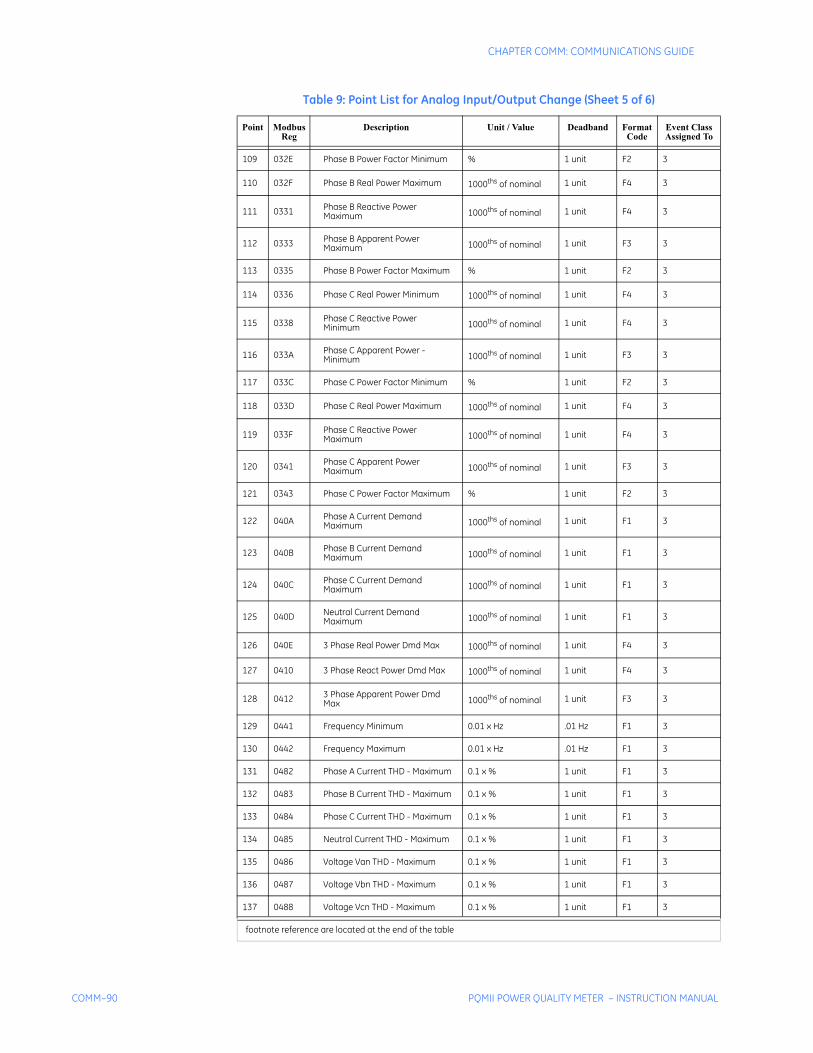
COMM–90 PQMII POWER QUALITY METER – INSTRUCTION MANUAL
CHAPTER COMM: COMMUNICATIONS GUIDE
109 032E Phase B Power Factor Minimum % 1 unit F2 3
110 032F Phase B Real Power Maximum 1000ths of nominal 1 unit F4 3
111 0331 Phase B Reactive Power Maximum 1000ths of nominal 1 unit F4 3
112 0333 Phase B Apparent Power Maximum 1000ths of nominal 1 unit F3 3
113 0335 Phase B Power Factor Maximum % 1 unit F2 3
114 0336 Phase C Real Power Minimum 1000ths of nominal 1 unit F4 3
115 0338 Phase C Reactive Power Minimum 1000ths of nominal 1 unit F4 3
116 033A Phase C Apparent Power - Minimum 1000ths of nominal 1 unit F3 3
117 033C Phase C Power Factor Minimum % 1 unit F2 3
118 033D Phase C Real Power Maximum 1000ths of nominal 1 unit F4 3
119 033F Phase C Reactive Power Maximum 1000ths of nominal 1 unit F4 3
120 0341 Phase C Apparent Power Maximum 1000ths of nominal 1 unit F3 3
121 0343 Phase C Power Factor Maximum % 1 unit F2 3
122 040A Phase A Current Demand Maximum 1000ths of nominal 1 unit F1 3
123 040B Phase B Current Demand Maximum 1000ths of nominal 1 unit F1 3
124 040C Phase C Current Demand Maximum 1000ths of nominal 1 unit F1 3
125 040D Neutral Current Demand Maximum 1000ths of nominal 1 unit F1 3
126 040E 3 Phase Real Power Dmd Max 1000ths of nominal 1 unit F4 3
127 0410 3 Phase React Power Dmd Max 1000ths of nominal 1 unit F4 3
128 0412 3 Phase Apparent Power Dmd Max 1000ths of nominal 1 unit F3 3
129 0441 Frequency Minimum 0.01 x Hz .01 Hz F1 3
130 0442 Frequency Maximum 0.01 x Hz .01 Hz F1 3
131 0482 Phase A Current THD - Maximum 0.1 x % 1 unit F1 3
132 0483 Phase B Current THD - Maximum 0.1 x % 1 unit F1 3
133 0484 Phase C Current THD - Maximum 0.1 x % 1 unit F1 3
134 0485 Neutral Current THD - Maximum 0.1 x % 1 unit F1 3
135 0486 Voltage Van THD - Maximum 0.1 x % 1 unit F1 3
136 0487 Voltage Vbn THD - Maximum 0.1 x % 1 unit F1 3
137 0488 Voltage Vcn THD - Maximum 0.1 x % 1 unit F1 3
Table 9: Point List for Analog Input/Output Change (Sheet 5 of 6)
Point Modbus Reg
Description Unit / Value Deadband Format Code
Event Class Assigned To
footnote reference are located at the end of the table
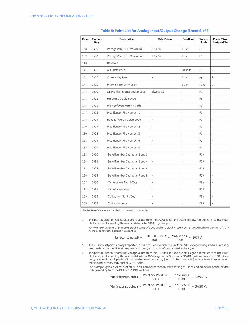
CHAPTER COMM: COMMUNICATIONS GUIDE
PQMII POWER QUALITY METER – INSTRUCTION MANUAL COMM–91
1. This point is used to reconstruct current values from the 1,000ths per-unit quantities given in the other points. Multi-ply the particular point by this one, and divide by 1000 to get amps.
For example, given a CT primary setpoint value of 3000 and an actual phase A current reading from the DUT of 1077A, the reconstructed phase A current is:
2. The VT Ratio setpoint is always reported, but is not used if a direct (i.e., without VTs) voltage wiring scheme is config-ured. In this case the VT Ratio setpoint is ignored, and a ratio of 1.0:1 is used in the PQMII.
3. This point is used to reconstruct voltage values from the 1,000ths per-unit quantities given in the other points. Multi-ply the particular point by this one, and divide by 1000 to get volts. Since some SCADA systems do not read 32 bit val-ues, you can also multiply the VT ratio and nominal secondary (both of which are 16 bit) in the master in cases wherethe nominal primary may exceed 32767 volts.For example, given a VT ratio of 300:1, a VT nominal secondary volts setting of 115 V, and an actual phase-neutralvoltage reading from the DUT of 19919 V, we have:
138 0489 Voltage Vab THD - Maximum 0.1 x % 1 unit F1 3
139 048A Voltage Vbc THD - Maximum 0.1 x % 1 unit F1 3
140 Reserved
141 04C8 ADC Reference - 20 units F1 2
142 04CB Current Key Press - 1 unit F81 2
143 04CC Internal Fault Error Code - 1 unit F108 2
144 0000 GE Multilin Product Device Code always 73 - F1 -
145 0001 Hardware Version Code - - F5 -
146 0002 Main Software Version Code - - F1 -
147 0003 Modification File Number 1 - - F1 -
148 0004 Boot Software Version Code - - F1 -
149 0007 Modification File Number 2 - - F1 -
150 0008 Modification File Number 3 - - F1 -
151 0009 Modification File Number 4 - - F1 -
152 000A Modification File Number 5 - - F1 -
153 0020 Serial Number Character 1 and 2 - - F10 -
154 0021 Serial Number Character 3 and 4 - - F10 -
155 0022 Serial Number Character 5 and 6 - - F10 -
156 0023 Serial Number Character 7 and 8 - - F10 -
157 0030 Manufacture Month/Day - - F24 -
158 0031 Manufacture Year - - F25 -
159 0032 Calibration Month/Day - - F24 -
159 0033 Calibration Year - - F25 -
Table 9: Point List for Analog Input/Output Change (Sheet 6 of 6)
Point Modbus Reg
Description Unit / Value Deadband Format Code
Event Class Assigned To
footnote reference are located at the end of the table
Ia(reconstructed) Point 0 Point 8×1000
----------------------------------------- 3000 359×1000
---------------------------- 1077 A= = =
Van reconstructed( ) Point 5 Point 14×1000
-------------------------------------------- 577 34500×1000
------------------------------- 19.91 kV= = =
Vbn reconstructed( ) Point 5 Point 18×1000
-------------------------------------------- 577 59756×1000
------------------------------- 34.50 kV= = =
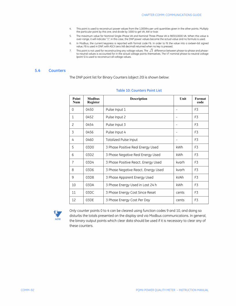
COMM–92 PQMII POWER QUALITY METER – INSTRUCTION MANUAL
CHAPTER COMM: COMMUNICATIONS GUIDE
4. This point is used to reconstruct power values from the 1,000ths per-unit quantities given in the other points. Multiplythe particular point by this one, and divide by 1000 to get VA, kW or kvar.
5. The maximum value for Nominal Single-Phase VA and Nominal Three-Phase VA is 983010000 VA. When this value isover-range, it will indicate “1”; in this case, the DNP power values become the actual value and no formula is used.
6. In Modbus, the current keypress is reported with format code F6. In order to fit the value into a sixteen-bit signedvalue, F8 is used in DNP, with ASCII zero (48 decimal) returned when no key is pressed.
7. This point is not used for reconstructing any voltage values. The difference between phase-to-phase and phase-to-neutral values is accounted for in the actual voltage points themselves. The VT nominal phase-to-neutral voltage(point 5) is used to reconstruct all voltage values.
5.4 CountersThe DNP point list for Binary Counters (object 20) is shown below:
Note Only counter points 0 to 4 can be cleared using function codes 9 and 10, and doing so disturbs the totals presented on the display and via Modbus communications. In general, the binary output points which clear data should be used if it is necessary to clear any of these counters.
3
Table 10: Counters Point List
Point Num
Modbus Register
Description Unit Format code
0 0450 Pulse Input 1 - F3
1 0452 Pulse Input 2 - F3
2 0454 Pulse Input 3 - F3
3 0456 Pulse Input 4 - F3
4 0460 Totalized Pulse Input - F3
5 03D0 3 Phase Positive Real Energy Used kWh F3
6 03D2 3 Phase Negative Real Energy Used kWh F3
7 03D4 3 Phase Positive React. Energy Used kvarh F3
8 03D6 3 Phase Negative React. Energy Used kvarh F3
9 03D8 3 Phase Apparent Energy Used kVAh F3
10 03DA 3 Phase Energy Used in Last 24 h kWh F3
11 03DC 3 Phase Energy Cost Since Reset cents F3
12 03DE 3 Phase Energy Cost Per Day cents F3