practical work book communication - ned university
TRANSCRIPT
PRACTICAL WORK BOOK
For Academic Session 2009
COMMUNICATION SYSTEMS
(TC-394)
For
TE (TC)
Name:
Roll Number:
Batch: Department: Year:
Department of Electronic Engineering NED University of Engineering & Technology, Karachi
LABORATORY WORK BOOK
For The Course
TC-394 COMMUNICATION SYSTEMS
Prepared By: Ms. Uzma Afsheen (Asst. Prof.)
Reviewed By: Mr. Tahir Malik (Lecturer)
Approved By: The Board of Studies of Department of Electronic Engineering

INTRODUCTION
Communication Systems Practical Workbook covers those practicals that are
very knowledgeable and quite beneficial in grasping the core objectives of
the subject. These practicals solidify the theoretical and practical concepts
that are very essential for the Telecommunications Engineering students.
This work book comprises of practicals covering the topics of the course
Communication Systems and are arranged on modern trainer boards and
contains relevant theory about the Lab sessions.
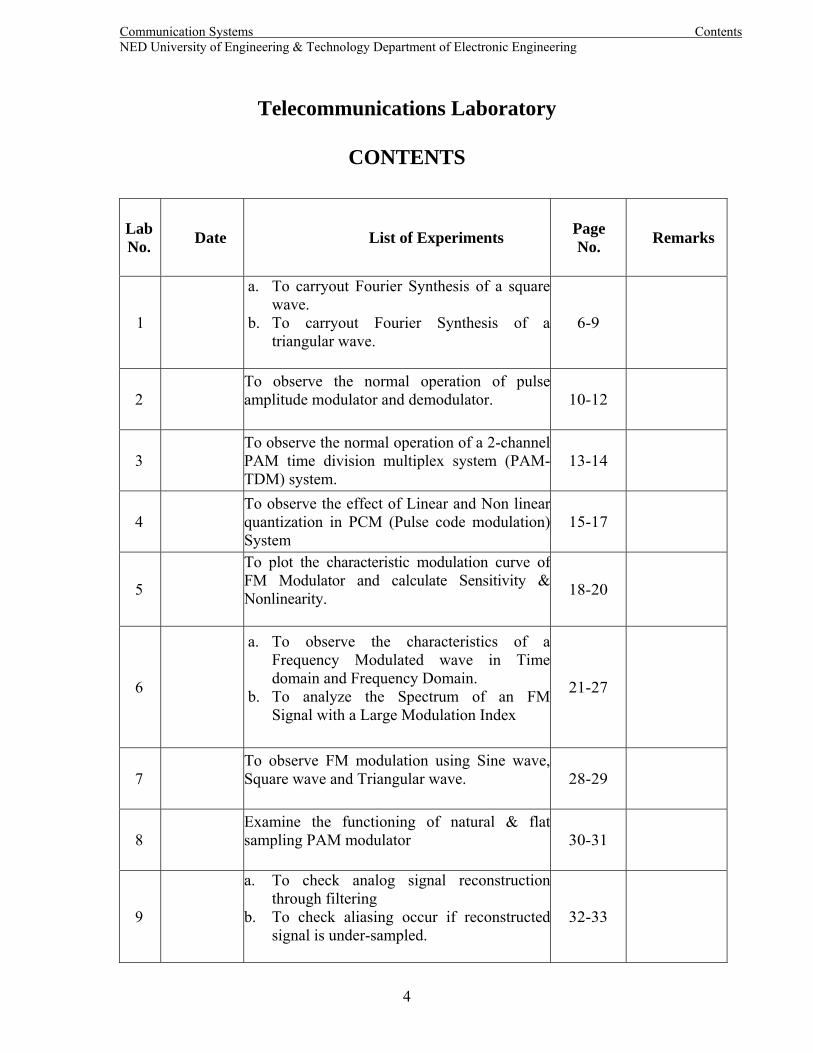
Communication Systems Contents NED University of Engineering & Technology Department of Electronic Engineering
Telecommunications Laboratory
CONTENTS
Lab No. Date List of Experiments Page
No. Remarks
1
a. To carryout Fourier Synthesis of a squarewave.
b. To carryout Fourier Synthesis of atriangular wave.
6-9
2 To observe the normal operation of pulse amplitude modulator and demodulator.
10-12
3 To observe the normal operation of a 2-channel PAM time division multiplex system (PAM-TDM) system.
13-14
4 To observe the effect of Linear and Non linearquantization in PCM (Pulse code modulation) System
15-17
5
To plot the characteristic modulation curve ofFM Modulator and calculate Sensitivity &Nonlinearity.
18-20
6
a. To observe the characteristics of aFrequency Modulated wave in Timedomain and Frequency Domain.
b. To analyze the Spectrum of an FM Signal with a Large Modulation Index
21-27
7 To observe FM modulation using Sine wave,Square wave and Triangular wave.
28-29
8 Examine the functioning of natural & flatsampling PAM modulator
30-31
9
a. To check analog signal reconstructionthrough filtering
b. To check aliasing occur if reconstructedsignal is under-sampled.
32-33
4
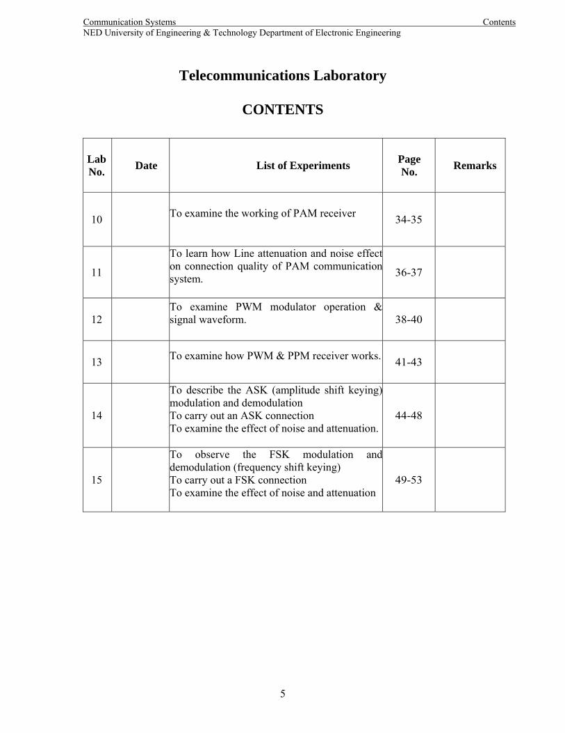
Communication Systems Contents NED University of Engineering & Technology Department of Electronic Engineering
Telecommunications Laboratory
CONTENTS
Lab No. Date List of Experiments Page
No. Remarks
10 To examine the working of PAM receiver 34-35
11
To learn how Line attenuation and noise effecton connection quality of PAM communicationsystem.
36-37
12 To examine PWM modulator operation &signal waveform.
38-40
13 To examine how PWM & PPM receiver works. 41-43
14
To describe the ASK (amplitude shift keying)modulation and demodulation To carry out an ASK connection To examine the effect of noise and attenuation.
44-48
15
To observe the FSK modulation anddemodulation (frequency shift keying) To carry out a FSK connection To examine the effect of noise and attenuation
49-53
5

Communication Systems Contents NED University of Engineering & Technology Department of Electronic Engineering
LAB SESSION 1(a)
OBJECT:-
a. To carryout Fourier Synthesis of a square wave. EQUIPMENT:- 1 Modules T10H. 1 +/- 12Vdc Supply 1 Oscilloscope. THEORY:- A square wave spectrum is made of the sum of all the harmonics being odd of the fundamental with decreasing amplitude according to the law of trigonometric fourier series. In other words the square wave shown in fig 2.1 can be obtained by summing up the infinite sine waves as per the following relation: S(t) = sin(2ΠFt)/1 + sin(2Π3Ft)/3 + sin(2Π5Ft)/5 + sin(2Π7Ft)/7 + sin(2Π9Ft)/9 + …….. PROCEDURE AND OBSERVATIONS:- 1- Odd harmonics (1, 3, 5, 7, 9): two way switches -/0/+ on + and two way switches sin/cos on sin. 2- Even harmonics (2, 4, 6, 8): two way switches -/0/+ on 0. 3- Connect the oscilloscope with the amplifier output of the fundamental (1st) and adjust the amplitude at 10Vp-p. ------------------------------------------------------------------------------------------------------- ------------------------------------------------------------------------------------------------------- ------------------------------------------------------------------------------------------------------- 4- Connect the oscilloscope with the output of the third harmonic amplifier (3RD) and adjust the amplitude at 10/3 ≈ 303Vp-p. ------------------------------------------------------------------------------------------------------- ------------------------------------------------------------------------------------------------------- ------------------------------------------------------------------------------------------------------- 5- Connect the oscilloscope with the output of the 5TH harmonic amplifier (5TH) and adjust the amplitude at 10/5 = 2Vp-p. ------------------------------------------------------------------------------------------------------- ------------------------------------------------------------------------------------------------------- ------------------------------------------------------------------------------------------------------- 6- Connect the oscilloscope with the output of the seventh harmonic amplifier (7TH) and adjust the amplitude at 10/7 ≈ 1.4Vp-p. ------------------------------------------------------------------------------------------------------- -------------------------------------------------------------------------------------------------------
6
Communication Systems NED University of Engineering & Technology Department of Electronic Engineering ------------------------------------------------------------------------------------------------------- 7- Connect the oscilloscope with the output of the 9th harmonic amplifier (9TH) and adjust the amplitude at 10/9 ≈ 1.1Vp-p ------------------------------------------------------------------------------------------------------- ------------------------------------------------------------------------------------------------------- ------------------------------------------------------------------------------------------------------- 8- Connect the oscilloscope with OUT and check that there is the signal corresponding to the components sum. ------------------------------------------------------------------------------------------------------- ------------------------------------------------------------------------------------------------------- ------------------------------------------------------------------------------------------------------- 9-Remove some harmonics (put the relating two way switch on 0) and check the o/p signal. ------------------------------------------------------------------------------------------------------- ------------------------------------------------------------------------------------------------------- ------------------------------------------------------------------------------------------------------- 10- Prove the Fourier series of square wave by using formula ∞
f(t) = a0 + ∑( an cos nwt + bn sin nwt) n=1
7
Communication Systems NED University of Engineering & Technology Department of Electronic Engineering
LAB SESSION 1(b)
OBJECT:-
b. To carryout Fourier Synthesis of a triangular wave. EQUIPMENT:- 1 Modules T10H. 1 +/- 12Vdc Supply 1 Oscilloscope. THEORY:- A triangular wave spectrum is made of the sum of all the harmonics being odd of the fundamental with decreasing amplitude according to the law of trigonometric fourier series. In other words the triangular wave can be obtained by summing up the infinite sine waves as per the following relation: S(t) = cos(2ΠFt)/1 + cos(2Π3Ft)/32 + cos(2Π5Ft)/52 + cos(2Π7Ft)/72 + cos(2Π9Ft)/92 + …….. PROCEDURE AND OBSERVATIONS:- 1- Odd harmonics (1, 3, 5, 7, 9): two way switches -/0/+ on + and two way switches sin/cos on cos. 2- Even harmonics (2, 4, 6, 8): two way switches -/0/+ on 0. 3- Connect the oscilloscope with the amplifier output of the fundamental (1st) and adjust the amplitude at 10Vp-p. ------------------------------------------------------------------------------------------------------- ------------------------------------------------------------------------------------------------------- ------------------------------------------------------------------------------------------------------- 4- Connect the oscilloscope with the output of the third harmonic amplifier (3RD) and adjust the amplitude at 10/32
------------------------------------------------------------------------------------------------------- ------------------------------------------------------------------------------------------------------- ------------------------------------------------------------------------------------------------------- 5- Connect the oscilloscope with the output of the 5TH harmonic amplifier (5TH) and adjust the amplitude at 10/52
------------------------------------------------------------------------------------------------------- ------------------------------------------------------------------------------------------------------- ------------------------------------------------------------------------------------------------------- 6- Connect the oscilloscope with the output of the seventh harmonic amplifier (7TH) and adjust the amplitude at 10/72
-------------------------------------------------------------------------------------------------------
8
Communication Systems NED University of Engineering & Technology Department of Electronic Engineering ------------------------------------------------------------------------------------------------------- ------------------------------------------------------------------------------------------------------- 7- Connect the oscilloscope with the output of the 9th harmonic amplifier (9TH) and adjust the amplitude at 10/92
------------------------------------------------------------------------------------------------------- ------------------------------------------------------------------------------------------------------- ------------------------------------------------------------------------------------------------------- 8- Connect the oscilloscope with OUT and check that there is the signal corresponding to the components sum. ------------------------------------------------------------------------------------------------------- ------------------------------------------------------------------------------------------------------- ------------------------------------------------------------------------------------------------------- 9-Remove some harmonics (put the relating two way switch on 0) and check the o/p signal. ------------------------------------------------------------------------------------------------------- ------------------------------------------------------------------------------------------------------- ------------------------------------------------------------------------------------------------------- 10- Prove the Fourier series of triangular wave by using formula ∞
f(t) = a0 + ∑( an cos nwt + bn sin nwt) n=1
9

Communication Systems NED University of Engineering & Technology Department of Electronic Engineering
LAB SESSION 02
OBJECT:-
• To observe the normal operation of pulse amplitude modulator and demodulator
EQUIPMENT:- • PAM Modulator module 736061 • PAM demodulator module 736071 • Function generator module 72695 • Power supply module 72686 • Frequency counter module 72699 • Oscilloscope • Bridging plugs & cable pairs
THEORY:- It is a modulation technique in which analog signal is sampled and sampled values arte used to modify certain parameters of a periodic pulse train to convert information into a form for transferring pulses from a source to a destination. There are two categories of pulse modulation:
• Digital pulse modulation • Analog pulse modulation
PAM is analog pulse modulation in which amplitude of a constant width and constant position pulse train is varied according to the amplitude of the analog signal. This process is termed as sampling of the analog signal. PAM signal is time discrete and value continuous. PAM signal is neither digital nor analog and it is not suitable for transmission. We are dealing with bipolar PAM as both positive and negative value arises. To avoid aliasing sampling theorem must be followed. PAM is used as an intermediate stage of the Pulse Code modulation PCM. PROCEDURE:-
• Set up the experiment. • Set the pulse generator to t/Tp = max and Fp = 15 kHz fed into the input filter
CH1 a sinusoidal signal with Fm = 500 Hz. • Observe the output of the filter by using oscilloscope with Vpp unchanged and
change Fm.
10
Communication Systems NED University of Engineering & Technology Department of Electronic Engineering
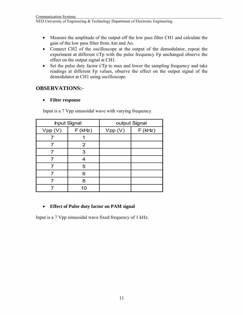
• Measure the amplitude of the output off the low pass filter CH1 and calculate the gain of the low pass filter from Am and Ao.
• Connect CH2 of the oscilloscope at the output of the demodulator, repeat the experiment at different t/Tp with the pulse frequency Fp unchanged observe the effect on the output signal at CH1.
• Set the pulse duty factor t/Tp to max and lower the sampling frequency and take readings at different Fp values, observe the effect on the output signal of the demodulator at CH1 using oscilloscope.
OBSERVATIONS:-
• Filter response Input is a 7 Vpp sinusoidal wave with varying frequency.
Vpp (V) F (kHz) Vpp (V) F (kHz)7 17 27 37 47 57 67 87 10
Input Signal output Signal
• Effect of Pulse duty factor on PAM signal Input is a 7 Vpp sinusoidal wave fixed frequency of 1 kHz.
11

Communication Systems NED University of Engineering & Technology Department of Electronic Engineering
Pulse Duty factor
Pulse Frequency
t/Tp Fp (kHz) Vpp (V) Fi (kHz) Vpp (V) Fo (kHz)50%40%30%20%10%
Input Signal Output Signal
• Effect of sampling frequency (Fp) on PAM signal Input is a 7 Vpp sinusoidal with fixed frequency of 1 kHz.
Pulse Duty factor
Pulse Frequency
t/Tp Fp (kHz) Vpp (V) Fi (kHz) Vpp (V) Fo (kHz)50%50%50%50%50%
Input Signal Output Signal
CONLCLUSION:- Give a brief analysis of:
• The effect of Pulse duty factor on the PAM signal:-
• The effect of the sampling frequency on the PAM signal:-
12
Communication Systems NED University of Engineering & Technology Department of Electronic Engineering
LAB SESSION 03
OBJECT:-
• To observe the normal operation of a 2-channel PAM time division multiplex system (PAM-TDM) system.
THEORY:- Multiplexing Multiplexing is the process of simultaneously transmitting more than one individual signals over a single communication link. Multiplexing has the effect of increasing the number of communication channels so that more information can be transmitted. There are two basic types of multiplexing:
• FDM (Frequency division multiplexing) • TDM (Time division multiplexing)
In TDM each signal can occupy the entire bandwidth of the channel however each channel is transmitted over a short period of time. PROCEDURE:-
• Set up the experiment as specified in the figure. • Feed the triangular shaped signal with frequency Fm1 = 200 Hz and amplitude
Am1 = 5V. in channel 1 (CH1). • Feed the sinusoidal signal with frequency Fm2 = 300Hz and amplitude Am2 = 6V
in channel 2 (CH2). • Set the sampling frequency to maximum i.e. Fp = 15 kHz. • Set the pulse duty factor to maximum i.e. t/Tp = 50%. • Display the input signals simultaneously on the oscilloscope and sketch these onto
diagram 1. • Display the PAM-TDM signal and sketch in diagram 1. • Display the respective input and output signal of the demodulator low pass filter
of CH1 and CH2 in diagram 2. • Display the clock signal and the demux trigger signal on the oscilloscope and set
∆t so that the trigger signal is delayed by 90o with respect to the clock signal. • Display the respective input and output signal of the demodulator low pass filter
of CH1 and CH2. • Adjust the ∆t with 180 degrees phase difference you will observe that the
demodulated signals from CH1 and CH2 are interchanged completely.
13
Communication Systems NED University of Engineering & Technology Department of Electronic Engineering
• Display the respective input and output signals of the demodulator low pass filter of CH1 and CH2.
• Now vary the pulse duty factor from ‘Min’ to ‘Max’ and see the effect at the output signal of CH1 and CH2 low pass filters. Alternate from PAM1 to PAM2 by changing the bridging plug at the PAM modulator.
• Connect the input of the low pass filter CH2 in the PAM demodulator with the output of the S & H stage by reconnecting the bridging plug at the low pass input.
OBSERVATIONS:-
Diagram 1: CH1, Ch2, PAM1 and PAM2 signals. Diagram 2: Input and output signals of CH1 and Ch2 low pass filters 00 delay. Diagram 3: Input and output signals of CH1 and CH2 low pass filters 900 delay. Diagram 4: Input and output signals of CH1 and CH2 low pass filters 1800 delay. Table 1: Influence of Sample and Hold (S & H) circuit in the demodulator
CH1 input signal
CH2 Input signal
Pulse factor t/Tp
Sampling frequency Fp
Output signal CH1 without
S & H
Output signal CH2 with
S & HVpp F1
Vpp F2
Variable Fixed (max)
Vpp F1
Vpp F2
6 V 5 V 10% 20 kHz6 V 5 V 20% 20 kHz6 V 5 V 25% 20 kHz6 V 5 V 30% 20 kHz6 V 5 V 35% 20 kHz6 V 5 V 40% 20 kHz6 V 5 V 45% 20 kHz
CONCLUSION:-
14

Communication Systems NED University of Engineering & Technology Department of Electronic Engineering
LAB SESSION 04 OBJECT:- To observe the effect of Linear and Non linear quantization in PCM (Pulse code modulation) System. EQUIPMENT:- 1 PAM modulator 736061 1 PAM demodulator 736071 1 PCM modulator 736101 1 PCM demodulator 736111 1 Function generator 0-200kHz 72695 1 Frequency counter 72699 1 Power supply 15V 1 Digital storage oscilloscope Bridging plugs Cable pairs THEORY:- Quantization means narrowing down of all possible signal values to a finite number. The quantization process takes an infinite number of all possible continuous signals. The quantization interval can be either equidistant discrete or logarithmic steps. In the case of equidistant quantization intervals this is referred to as linear quantization. In the case of logarithmic steps this is called non linear quantization. The quantization becomes more precise with an increasing number of steps and there is a decrease in the quantization noise. PROCEDURE:- 1. Use the experiment setup according to figure. 2. By pressing the MODE button several times switch to the operating mode: PCM
linear quantization (recognizable when the appropriate LED lights up). 3. Enable all of the bits. For this press the push button SELECT until all (red) LEDs
on the PCM modulator indicate ACTIVE. 4. Connect the DC voltage source of the PCM modulator as the input U1. 5. The quantified voltage is U2 and can be tapped at the D/A converter of the PCM
demodulator. 6. Set to -9.5V on the 10 stage potentiometer. 7. Alternately measure U1 and U2 using the multimeter and note down the voltages
together with the binary coded bit sequence of the PCM bit modulator in Table.
15

Communication Systems NED University of Engineering & Technology Department of Electronic Engineering 8. The bit sequence is displayed by LEDs whereby the LSB is at the top. 9. Now increase the input voltage U1 in steps of approx. 1V and repeat the recording
of the measurement value until the upper modulation limit of the PCM modulator is reached.
10. Display the curve of U2 versus U1 as a quantization characteristic in graph. 11. By pressing the MODE push button on the PCM modulator several times switches
to the operating mode: PCM non linear quantization. The PCM demodulator remains in linear operation.
12. Record the compressor characteristic. Proceed in the same manner as for the recording of the linear quantization characteristic in Table.
13. Plot the curve of U2 versus U1 as a compressor characteristic in graph. 14. For expander characterstic set the PCM modulator to linear quantization & PCM
demodulator to non linear quantization. 15. Plot the curve of U2 versus U1 as an expander characteristic in graph. 16. In order to record the Non linear transmission characteristic switch the PCM
modulator and demodulator to non linear mode. Record the transmission characteristic in table & Plot the curve of U2 versus U1 in graph.
OBSERVATION AND RESULT:- Linear Quantization Characteristic U1 Volts, Bit pattern
U2 Volts, Bit pattern
U1 Volts, Bit pattern
U2 Volts, Bit pattern
-9, -8, 1, -7, 2, -6, 3, -5, 4, -4, 5, -3, 6, -2, 7, -1, 8, 0, 9,
16

Communication Systems NED University of Engineering & Technology Department of Electronic Engineering Non-linear quantization Compressor characteristic U1 Volts, Bit pattern
U2 Volts, Bit pattern
U1 Volts, Bit pattern
U2 Volts, Bit pattern
-9, 0 -8, 1, -7, 2, -6, 3, -5, 4, -4, 5, -3, 6, -2, 7, -1, 8, 0, 9, Non-linear quantization Expander characteristic U1 Volts, Bit pattern
U2 Volts, Bit pattern
U1 Volts, Bit pattern
U2 Volts, Bit pattern
-9, 0 -8, 1, -7, 2, -6, 3, -5, 4, -4, 5, -3, 6, -2, 7, -1, 8, 0, 9, Non-linear Transmission Characteristic U1 Volts, Bit pattern
U2 Volts, Bit pattern
U1 Volts, Bit pattern
U2 Volts, Bit pattern
-9, 0 -8, 1, -7, 2, -6, 3, -5, 4, -4, 5, -3, 6, -2, 7, -1, 8, 0, 9,
17
Communication Systems NED University of Engineering & Technology Department of Electronic Engineering
LAB SESSION 05 OBJECT:-
• To plot the characteristic modulation curve of FM Modulator and calculate Sensitivity & Nonlinearity.
EQUIPMENT:-
• Modules T10A-T10B • +/- 12 V dc power supply. • Oscilloscope. • Voltmeter.
THEORY:- Frequency Modulation Generation The circuits used to generate a frequency modulation must vary the frequency of a high frequency carrier signal as a function of the amplitude of low frequency signal (modulation signal). In practice there are two main methods used to generate FM:
• Direct method: a tank circuit is used in which the reactance of one of the elements of the resonant circuit depends on the modulating voltage. The most common device with variable reactance is the Varactor or Varicap. This is a particular diode and its capacitance varies according to the reverse bias voltage applied across it. The frequency of the carrier is established with Automatic Frequency Control (AFC) circuits or Phase Lock Loop (PLL).
• Indirect method: The FM is obtained in this case by a Phase modulation, after the modulating signal has been integrated. In the phase modulator the carrier can be generated by a quartz oscillator, and so its frequency stabilization is easier.
In the circuit used, the frequency modulation is generated by a Hartley oscillator, with its frequency is determined by a fixed inductance and by the capacitance supplied by the Varicap diode. Characteristic Modulation curve, Sensitivity & Non linearity The characteristic modulation curve is given by the output frequency of the modulator as a function of the input modulating voltage. It is possible to plot the curve point by point to statistically simulate an amplitude variation of the modulating signal, and measure the corresponding output frequency of the modulator.
18
Communication Systems NED University of Engineering & Technology Department of Electronic Engineering PROCEDURE:-
• Power the module T10A with +/-12 V dc and carry out the following presetting:
VCO 1: Level about 2 Vpp: FREQ. to the minimum: switch on 1500 kHz. • Connect the oscilloscope to the output of the modulator (FR/FM OUT, point 19). • Connect the voltmeter to the cursor of the frequency regulation potentiometer
(point 17). • Vary the Voltage at steps of 0.5 V and fill a table with the voltage values and the
corresponding frequencies. • Plot a graph with the measured voltage and frequency values. You will obtain a
curve. • From the analysis of the curve you can note that some segments do not have a
linear behavior, while if you consider the whole characteristic you find a high non-linearity.
• Consider to make the modulator operate in the segment of curve within 700 and 1300 kHz, with central frequency of 1000 kHz. By analysis of the curve it is possible to calculate the modulation sensitivity and the non-linearity of the modulator.
• The modulation sensitivity is defined as :
S = d F(v) / d V Where F(v) is the instantaneous frequency function of the modulating voltage V. this relation can be approximated by writing the incremental ratio: S = ∆F / ∆V
• The nonlinearity N.L. of the modulator is defined as percentage relative shift of the
sensitivity S from the SO value corresponding to the central frequency:
N.L = [(S- SO) / SO] x 100
OBSERVATION & CALCULATION:- Input Voltage (V dc) Output Frequency (F kHz)
19
Communication Systems NED University of Engineering & Technology Department of Electronic Engineering With reference to the curve plotted Central frequency = ____________ ∆F = _________ ∆V = _________ Sensitivity SO = ∆F / ∆V = ∆F1 = __________ ∆V1 = __________ Sensitivity S1 = ∆F1 / ∆V1 = (N.L)1 = (S1 - SO) / SO = ∆F2 = ___________ ∆V2 = ___________ Sensitivity S2 = ∆F2 / ∆V2 = (N.L)2 = (S2 - SO) / SO =
RESULT:-
20

Communication Systems NED University of Engineering & Technology Department of Electronic Engineering
LAB SESSION 6(a) OBJECTIVE:- To observe the characteristics of a Frequency Modulated wave in Time domain and Frequency Domain. EQUIPMENT:- Feedback-Teknikit Console 92-300. Pentium 4 or equivalent computer available in lab. THEORY:- Frequency Modulation Generation: The circuits used to generate a frequency modulation must vary the frequency of a high frequency carrier signal as a function of the amplitude of low frequency signal (modulation signal). In practice there are two main methods used to generate FM:
• Direct method: a tank circuit is used in which the reactance of one of the elements of the resonant circuit depends on the modulating voltage. The most common device with variable reactance is the Varactor or Varicap. This is a particular diode and its capacitance varies according to the reverse bias voltage applied across it. The frequency of the carrier is established with Automatic Frequency Control (AFC) circuits or Phase Lock Loop (PLL).
• Indirect method: The FM is obtained in this case by a Phase modulation, after the modulating signal has been integrated. In the phase modulator the carrier can be generated by a quartz oscillator, and so its frequency stabilization is easier.
PROCEDURE:- Begin by powering up the PC and trainer board. After that click on the Discovery II IMS window and scroll to the required practical as shown in figure 1.
21

Communication Systems NED University of Engineering & Technology Department of Electronic Engineering
Figure 1
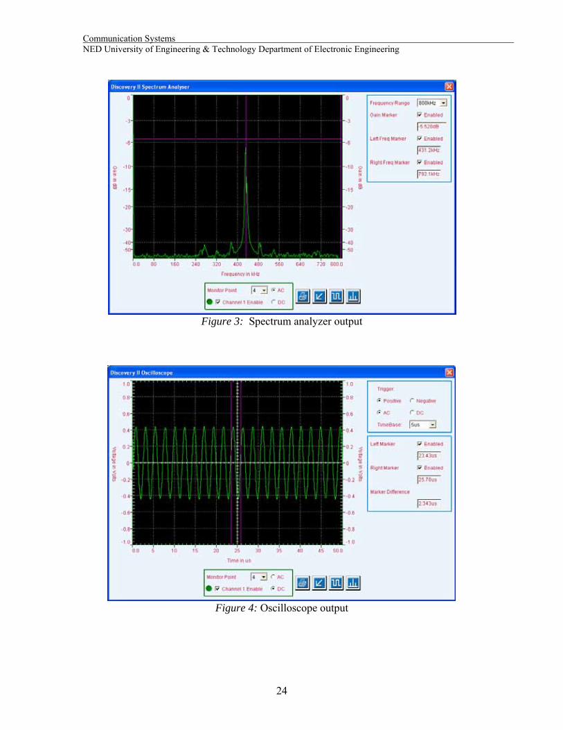
Click on the green icon named ‘Practical’ (its folder titled ‘Practical 1: Concepts of Frequency Modulation’ -see above). Accept the pop up that appears after clicking on the ‘Practical’ link to start the in built oscilloscope interface. You have available an oscilloscope and a spectrum analyzer. Using this configuration you can see how the oscillator frequency can be controlled by an external signal. Set Carrier level to about half scale (0.8 Vp-p). Monitor point 16 shows us the DC input voltage and monitor point 4 shows the output carrier which is frequency modulated. Figure 2 shows the output signal when input voltage is 0 V. you can measure the frequency in the time domain using the oscilloscope and also in the frequency domain using the spectrum analyzer.
22

Communication Systems NED University of Engineering & Technology Department of Electronic Engineering
Figure 2
The Frequency corresponding to a zero input voltage is best observed by the spectrum analyzer as shown in figure 3. The left marker of the spectrum analyzer is utilized to measure the signal frequency. A tedious way to measure the output signal frequency is by observing the signal in time domain. We take the inverse of the pulse time duration which is measured with the help of the left and right scope markers-Figure 4. Note, that the spectrum analyzer method is a bit more accurate.
23
Communication Systems NED University of Engineering & Technology Department of Electronic Engineering
Figure 3: Spectrum analyzer output
Figure 4: Oscilloscope output
24

Communication Systems NED University of Engineering & Technology Department of Electronic Engineering OBSERVATION:- Set the carrier amplitude such that it is 2 divisions above and below the x-axis (approximately 0.8 Vp-p). Fill in the table below for DC input voltage vs. output carrier frequency. Plot a graph using the values you recorded in the table.
Input Voltage (V)
Output Frequency (Oscilloscope) Hz
Output Frequency (Spectrum Analyzer) Hz
RESULT:-
25

Communication Systems NED University of Engineering & Technology Department of Electronic Engineering
LAB SESSION 6(b) OBJECT:- To analyze the Spectrum of an FM Signal with a Large Modulation Index EQUIPMENT:- 1 Frequency Modulation 53-140 module 1 Oscilloscope. THEORY:- This is a simple practical where the frequency modulator is connected to the spectrum analyser.The carrier frequency has been reduced to about 5 kHz so, since the maximum deviation is the same, the modulation index is much greater. The bandwidth is: B = 2 ( F +F )d m where B is the bandwidth, Fd the deviation and Fm is the bandwidth of the modulation. So if Fm is small compared with Fd, i.e the modulation index is large, then
B = 2 Fd On the analyser the spectrum appears to be continuous but in reality it is made up of a large number of sidebands spaced at 5KHz intervals from the carrier up to Fd. This practical simply shows how when the modulation index is large the bandwidth is determined almost exclusively by the deviation. PROCEDURE:- 1. In this practical the modulation frequency has been set to 5kHz. This means that the modulation index can be very high. 2. This enables you to see that under these conditions the bandwidth of an FM signal is almost equal to twice the deviation. 3. Set Carrier level to about half scale. 4. Turn the 5kHz level up and down and observe the bandwidth changing. Note that the bandwidth is almost proportional to the deviation OBSERVATIONS:- ------------------------------------------------------------------------------------------------------------------------------------------------------------------------------------------------------------------------------------------------------------------------------------------------------------------------------------------------------------------------------------------------------------------------------------------------------------------------------------------------------------------------------------------------------------
26

Communication Systems NED University of Engineering & Technology Department of Electronic Engineering ------------------------------------------------------------------------------------------------------------------------------------------------------------------------------------------------------------------------------------------------------------------------------------------------------------------------------------------------------------------------------------------------------------------------------------------------------------------------------------------------------------------------------------------------------------------------------------------------------------------------------------------------------------------------------------------------------------------------------------------------------------------------------------------------------------------------------------------------------------------------------------------ ------------------------------------------------------------------------------------------------------------------------------------------------------------------------------------------------------------------ RESULT:-
27
Communication Systems NED University of Engineering & Technology Department of Electronic Engineering
LAB SESSION 07 OBJECT:- To observe FM modulation using Sine wave, Square wave and Triangular wave. EQUIPMENT:- Modules T10A-T10B +/- 12-V dc power supply Oscilloscope Voltmeter.
THEORY:- Frequency Modulation is a system in which the amplitude of the modulated carrier is kept constant, while its frequency is varied by the modulating signal. Unlike Amplitude Modulation, FM is, or can be made, relatively immune to noise. The effect of noise depends on the noise sideband frequency. Processes of pre-emphasis and de-emphasis plays an important part in making FM immune to noise. The first practical FM system was put forward in 1936 as an alternative to AM to make radio transmissions more resistant to noise. A comparison of FM and AM reveals:
• The amplitude of an exponential modulated wave is constant. • The message resides in the zero-crossings alone, provided the carrier frequency is
large. • The modulated wave is not at all like the message waveform.
OBSERVATION:- It has been observed that as the voltage level of baseband signal increases the frequency of the signal after modulation also increases for all types of signals as shown. Sine Wave As voltage of sine wave increases the frequency increases as well.
28

Communication Systems NED University of Engineering & Technology Department of Electronic Engineering Square Wave At high level the frequency increases and at the low level the frequency of FM decreases. Triangular Wave As voltage increases the frequency of carrier increases and as voltage decreases the frequency of carrier decreases. RESULT:-
29
Communication Systems NED University of Engineering & Technology Department of Electronic Engineering
LAB SESSION 08 OBJECT:- Examine the functioning of natural, flat sampling PAM modulator EQUIPMENT:- Module T20A Power supply oscilloscope THEORY:- PAM: A PAM signal is a sampling signal made up by a series of pulses whose amplitude is proportional to an analog signal amplitude. Sampling can be of normal & flat type. Flat sampling results in distortion of reconstructed signal as τ pulse duration increases. This sampling is used in PCM system. Natural sampling PAM modulator: Block diagram mounted in model have an i/p analog signal passes through a 3.5KHz low pass filter which eliminates aliasing effect when sampling frequency is 8 or 12 kHz.. then the signal goes to sampler. Sampling freq in timing section can be selected at 4,8,12kHz. Sampling pulse width is determined by pulse generator section. Flat sampling PAM modulator: In comparison with natural sampling modulator, a sample & hold ckt is added which fixes the o/p signal amplitude 7 keeps it steady on the i/p value recorded in sampling. Sampler produces flat peak pulses whose width is proportional to analog signal width. PROCEDURE & OBSERVATIONS:-
1. Supply ±12V power & carryout following presettings: Timing:J1=8khz, pulse generator: completely turn pulse width clockwise
2. Connect TP13 to TP3 & short J3 for natural sampling 3. Check i/p analog signal at TP13 & PAM modulator o/p TP12
------------------------------------------------------------------------------------------------------------------------------------------------------------------------------------------------------------------------------------------------------------------------------------------------------------------------------------
4. Check that PAM signal is formed by train of pulses having an amplitude which reflects analog signal w/f.
30

Communication Systems NED University of Engineering & Technology Department of Electronic Engineering
5. Move probe from TP13 to TP11, check that sampling pulses tally with PAM signal.
------------------------------------------------------------------------------------------------------------------------------------------------------------------------------------------------------------------------------------------------------------------------------------------------------------------------------------
6. Change sampling pulse width & observe corresponding variation of PAM signal. 7. Now short J3 = flat sampling w/o changing previous settings. 8. Examine again w/f of i/p signal TP13, sample & hold o/p signal TP5 & of S/H
sampling pulses TP4 ------------------------------------------------------------------------------------------------------------------------------------------------------------------------------------------------------------------------------------------------------------------------------------------------------------------------------------
9. Notice that signal is sampled at the beginning of sampling pulse & its amplitude is kept steady until next pulse. A step signal is obtained which approximates i/p analog signal
10. Examine w/f at sampling pulses for PAM modulate TP11 & o/p PAM signal TP12. Notice that step signal is sampled when its value is steady.
11. Notice that PAM pulse show const amplitude over their whole duration. 12. Change sampling pulse width & observe corresponding variation of PAM signal
------------------------------------------------------------------------------------------------------------------------------------------------------------------------------------------------------------------------------------------------------------------------------------------------------------------------------------------------------------------------------------------------------------------------------------------------------------------------------------------------------------------------------------------------------ ------------------------------------------------------------------------------------------------------------------------------------------------------------------------------------------------------------------------------------------------------------------------------------------------------------------------------------------------------------------------------------------------------------------------------------------------------------------------------------------------------------------------------------------------------ ------------------------------------------------------------------------------------------------------------------------------------------------------------------------------------------------------------------------------------------------------------------------------------------------------------------------------------------------------------------------------------------------------------------------------------------------------------------------------------------------------------------------------------------------------ RESULT:-
31

Communication Systems NED University of Engineering & Technology Department of Electronic Engineering
LAB SESSION 9 OBJECT:- a. To check analog signal reconstruction through filtering b. To check aliasing occur if reconstructed signal is undersampled
EQUIPMENT:- Module T20A Power supply oscilloscope THEORY:- Analog signal reconstruction from samples is performed with a LPF. When sampling frequency equals 2B, an ideal LPF with a F/2 pass band can perfectly extract the same spectrum as original signal. If the filter is not an ideal one, there will be a section of spectrum S(f) centered around f which is super imposed on the section of spectrum to be extracted by filter which alters reconstruction of s(t). if sampling frequency is increased filtering becomes easier as repetitions of s(t) signal spectrum are spaced out. If sampling frequency is decreased , aliasing may occur. Sampling a signal with a lower frequency than theoretical value or using a filter with an insufficient band to reconstruct original signal causes “aliasing effect PROCEDURE & OBSERVATIONS:- A:
1. Generate a flat sampling PAM signal by connecting TP 13 to TP3, jumper J3=flat, J1=8khz.
2. Remove J8 jumper (if connected) & connect modulator o/p TP12 with 3.4khz LPF i/p TP 24
3. At TP26, examine the w/f of reconstructed ckt. Check that this signal shows slight distortion due to faulty suppression of sampling frequency (8khz)
------------------------------------------------------------------------------------------------------------------------------------------------------------------------------------------------------------------------------------------------------------------------------------------------------------------------------------
4. Cascadely connect 5khz & 3.4 khz filter TP26 to TP 25 & check reconstructed o/p signal at TP27, this will increase overall filter selectivity. Check that distortion nearly disappears.
5. Change the pulse width of PAM & observe how reconstructed signal amplitude change.
32

Communication Systems NED University of Engineering & Technology Department of Electronic Engineering
6. Now maintain previous setting but select J1=12khz. At TP26 when 3.4khz filter is only selected examine the w/f of reconstructed signal. Check that signal show far low distortion in comparison with 8khz sampling.
--------------------------------------------------------------------------------------------------------------------------------------------------------------------------------------------------------------------------------------------------------------------------------------------------------------------- 7. Now select J1=4khz & analyse the signal explaining the reason why it is
considerably distorted.
B: 1. Generate a flat sampling PAM signal by connecting TP 14(5khz i/p signal) to
TP3, jumper J3=flat, J1=8khz 2. With an oscilloscope examine TP3 analog signal, sampling pulses(TP11) & PAM
signal (TP12). From analysis of above w/f it is possible to check: • Samples vary according to sinusoidal signal • An average of 2 samples per period is recorded.
------------------------------------------------------------------------------------------------------------------------------------------------------------------------------------------------------------------------------------------------------------------------------------------------------------------------------------------------------------------------------------------------------------------------------------------------
3. Remove J8 jumper (if connected) & cascadely connect 5khz & 3.4 khz filter TP27 to TP 24, this will increase overall filter selectivity. Then connect modulator o/p with 5khz filter(TP12 with TP25)
4. In TP26 examine the w/f of reconstructed signal. A slight distortion is found having an approximate freq of 3khz
------------------------------------------------------------------------------------------------------------------------------------------------------------------------------------------------------------------------------------------------------------------------------------------------------------------------------------
5. Apply signal to modulator through i/p LPF (TP14 to TP1), check reception signal (TP26) erroneously reconstructed because aliasing effect is considerably reduced
6. Bypass i/p filter again( connect TP14 to 3) & J1=12khz 7. Examine o/p signal coming out of 5khz filter (TP27) & check that reconstructed
signal is same as original signal. ------------------------------------------------------------------------------------------------------------------------------------------------------------------------------------------------------------------------------------------------------------------------------------------------------------------------------------------------------------------------------------------------------------------------------------------------------------------------------------------------------------------------------------------------------------ ------------------------------------------------------------------------------------------------------------------------------------------------------------------------------------------------------------------------------------------------------------------------------------------------------------------------------------ RESULT:-
33

Communication Systems NED University of Engineering & Technology Department of Electronic Engineering
LAB SESSION 10
OBJECT:- To examine the working of PAM reciever EQUIPMENT:- Module T20A Power supply oscilloscope THEORY:- In order to demodulate PAM signal , a LPF is enough. This solution doesnot guarantee good connection quality & cannot be used in PAM- TDM. Therefore PAM receiver is constructed according to: PAM pulses coming from transmitter are sampled by sampling signal which is regenerated in receiver itself. Sampler o/p is kept at steady level until sample arrives, thereby generating a step signal. The signal reconstructed from step signal has a wider amplitude than signal reconstructed directly from PAM pulses. Receiver block diagram: PAM signal coming from transmitter is amplified & applied to 2 sections: sampling pulse regenerator & demodulator (S/H). the demodulator o/p signal is filtered through LPF which produces demodulated analog signal. Regeneration of sampling pulses for demodulator is carried out as follows: Amplified PAM signal passes through a limiting ckt which reduces signal amplitude variations. The next BPF(adjusted at 8 or 12 kHz) separates sampling frequency component. Such component gets to PLL which generates a synchronous sampling signal with PAM pulses it receives. The next ckt adjust the phase of pulses coming from PLL. PROCEDURE & OBSERVATIONS:-
1. Generate a flat sampling PAM signal presetting transmitter by connecting TP 13 to TP3(1khz i/p signal), jumper J3=flat, J1=8khz.
2. Preset receiver J6=8khz, J7=8khz, J8= PAM 3. Connect transmitter o/p TP 12 with line i/p TP15 & line o/p P16 to reciver i/p
TP17. Bring line attenuation to minimum & remove jumper(if connected) which selects line band pass.
4. Examine w/f at amplifier i/p & o/p(TP17 & 18). O/p pulses have wider amplitude & are slightly distorted.
------------------------------------------------------------------------------------------------------------------------------------------------------------------------------------------------------------------------------------------------------------------------------------------------------------------------------------------------------------------------------------------------------------------------------------------------
34

Communication Systems NED University of Engineering & Technology Department of Electronic Engineering
5. Examine signal after limiter TP19 & note considerable decrease of pulse amplitude variation.
------------------------------------------------------------------------------------------------------------------------------------------------------------------------------------------------------------------------------------------------------------------------------------------------------------------------------------------------------------------------------------------------------------------------------------------------
6. At filter o/p TP20, an almost sinusoidal w/f is obtained having same frequency as PAM pulses at receiver i/p.
7. At PLL o/p TP21, if PLL locked a square w/f is obtained having same frequency as PAM pulses at receiver i/p.
------------------------------------------------------------------------------------------------------------------------------------------------------------------------------------------------------------------------------------------------------------------------------------------------------------------------------------------------------------------------------------------------------------------------------------------------
8. Examine PAM signal at amplifier o/p TP18 together with generated sampling pulses coming from Phase Adjust ckt. Check that sampling pulses can be brought exactly to middle of PAM pulses through Phase adjust potentiometer. This enables demodulator to sample PAM signal exactly when pulse amplitude achieves its maximum value.
9. Examine w/f at demodulator i/p & o/p (TP 18 & 24). Rotate phase adjust in order to obtain maximum step signal amplitude at demodulator o/p
10. Examine signal w/f at reception filter o/p (TP26) & check if it is same as transmitted analog signal(TP1)
------------------------------------------------------------------------------------------------------------------------------------------------------------------------------------------------------------------------------------------------------------------------------------------------------------------------------------------------------------------------------------------------------------------------------------------------------------------------------------------------------------------------------------------------------ ------------------------------------------------------------------------------------------------------------------------------------------------------------------------------------------------------------------------------------------------------------------------------------------------------------------------------------------------------------------------------------------------------------------------------------------------------------------------------------------------------------------------------------------------------ ------------------------------------------------------------------------------------------------------------------------------------------------------------------------------------------------------------------------------------------------------------------------------------------------------------------------------
RESULT:-
35

Communication Systems NED University of Engineering & Technology Department of Electronic Engineering
LAB SESSION 11
OBJECT:- To learn how Line attenuation and noise effect on connection quality of PAM communication system. EQUIPMENT:- Module T20A Power supply oscilloscope THEORY:- The block diagram of the communication system is shown in fig. 7.1. The PAM signal is transmitted through an artificial line whose length (attenuation) and band-pass can be changed to -3dB (5/10/20/40KHz). The noise generator allows to add noise to the PAM signal, in order to obtain a noise-affected PAM signal at the line out put. Since the information carried by a PAM signal is contained in the amplitude of its pulses, any thing superimposed on the pulses can change the original pulse amplitude. As a result of it, the PAM demodulator output is distorted in comparison with of original starting signal. In addition to noise, the communication channel band-pass also influences the quality of the receiver signal. Inadequate width of the communication channel band can distort the PAM pulses, thereby worsening the signal/noise ratio at the receiver input and consequently lowering the quality of the received signal. PROCEDURE & OBSERVATIONS:-
1. Generate a flat sampling PAM signal presetting transmitter by connecting TP 13 to TP3(1kHz i/p signal), jumper J3=flat, J1=8khz.
2. Preset receiver J6=8kHz, J7=8kHz, J8= PAM 3. connect transmitter o/p TP 12 with line i/p TP15 & line o/p P16 to receiver i/p
TP17. Bring line attenuation to minimum & remove jumper (if connected) which selects line band pass.
4. gradually increase noise & examine w/f at line i/p & o/p (TP 15 & 16). o/p pulse is continuously variable because of noise
5. examine w/f at demodulator o/p (TP24) & notice how noise signal changes step signal amplitude. Rotate phase adjust in order to obtain maximum signal amplitude.
------------------------------------------------------------------------------------------------------------------------------------------------------------------------------------------------------------------------------------------------------------------------------------------------------------------------------------
36

Communication Systems NED University of Engineering & Technology Department of Electronic Engineering
6. examine w/f in clock regenerating circuits(TP 19,20,21,22). Notice that jitter increases as noised increases.
------------------------------------------------------------------------------------------------------------------------------------------------------------------------------------------------------------------------------------------------------------------------------------------------------------------------------------
7. the locking loss is also highlighted by diminished brightness of LOCK LED. This shows that noise induced in demodulated signal distortion is due to amplitude variation of PAM pulses & instability of sampling pulses regenerated during reception.
8. examine PAM w/f at line i/p & o/p (TP 15 & 16). Change line bandpass. Notice that as band is reduced, the pulse distortion increases & their amplitude decreases.
------------------------------------------------------------------------------------------------------------------------------------------------------------------------------------------------------------------------------------------------------------------------------------------------------------------------------------------------------------------------------------------------------------------------------------------------
9. examine w/f at demodulator o/p (TP24) & reception filter o/p TP26. notice that band gets narrower, detected sigal amplitude decreases. Rotate phase adjust in order to obtain maximum signal amplitude.
10. now use microphone signal as modulating signal & connect headphone with 3.4 kHz o/p TP26. listen to reception signal as following condition vary: phase adjust, noise, bandpass & line attenation, sampling frequency
------------------------------------------------------------------------------------------------------------------------------------------------------------------------------------------------------------------------------------------------------------------------------------------------------------------------------------------------------------------------------------------------------------------------------------------------------------------------------------------------------------------------------------------------------------ ------------------------------------------------------------------------------------------------------------------------------------------------------------------------------------------------------------------------------------------------------------------------------------------------------------------------------------ ------------------------------------------------------------------------------------------------------------------------------------------------------------------------------------------------------------------------------------------------------------------------------------------------------------------------------------------------------------------------------------------------------------------------------------------------------------------------------------------------------------------------------------------------------------ ------------------------------------------------------------------------------------------------------------------------------------------------------------------------------------------------------------------------------------------------------------------------------------------------------------------------------------ RESULT:-
37

Communication Systems NED University of Engineering & Technology Department of Electronic Engineering
LAB SESSION 12 OBJECT:- To examine PWM modulator operation & signal waveform. EQUIPMENT:- Module T20A Power supply oscilloscope THEORY:- A Pulse carrier can be modulation as concerns its amplitude or its timing. This second case is usually defined as pulse Time Modulation (PTM): two instances of PTM are pulse width Modulation (PWM) and pulse position Modulation (PPM). A PWM signal is a pulse signal whose pulse width is proportional to the modulating analog signal amplitude . The PWM signal is also used to generate the PPM signal. This is a pulse signal whose pulse position is proportional to the modulating analog signal amplitude. The PPM pulses are usually generated by the descending front of the PWM pulses. PWM Modulator The block diagram of the PWM modulator mounted on the module is shown in fig. The PMW modulator proper includes a stage comparator, which compares the respective amplitude of:
• a PAM signal obtained by sampling the input analog signal • a sampling-pulse-synchronous ramp signal.
The comparator switch the output when the PAM signal amplitude exceeds the ramp signal amplitude: this results into a pulse signal whose pulse duration depends on the amplitude of the input analog signal. from the modulator waveforms indicated in fig. notice that the PWM pulse trailing edge corresponds to the sampling pulses, whereas the (variable) leading edge corresponds to the comparator switching. PPM Modulator The block diagram of the PPM modulator mounted on the module is shown fig. The PPM signal is obtained form the PWM signal, by generating fixed-duration pulse which correspond to the leading edges of the PWM signal. This result into a train of pulse whose position depends on the input analog signal.
38

Communication Systems NED University of Engineering & Technology Department of Electronic Engineering
PROCEDURE & OBSERVATIONS:-
1. Perform the connections. Supply the ±12V power and carry out the following per-setting. -TIMING: 8KHz -SAWTOOTH GENRATOR: 8KHz
2. Connect the oscilloscope with the input analog signal (TP1) and with the sampler output (TP5)
-----------------------------------------------------------------------------------------------------------------------------------------------------------------------------------------------------------------------------------------------------------------------------------------------------------------------------------
3. Verify that the sampled signal is made up by a series of steps whose amplitude depends on the analog signal waveform
4. move the probe from TP1 to TP , check that the SAWTOOTH GENERATOR supplies an approximate ramp of +3V : -3V for each sampling interval.
5. move the probe form TP6 to TP8 (PWM modulator output). Synchronise the oscilloscope with the PAM signal (TP5) and verify the following:
- The trailing edge of the pulses corresponds to the sampling pulses - The leading edge – and consequently the duration of the PWM pulses – varies according to the PAM signal amplitude and corresponds to the instant in which the PAM exceeds the ramp signal.
------------------------------------------------------------------------------------------------------------------------------------------------------------------------------------------------------------------------------------------------------------------------------------------------------------------------------------------------------------------------------------------------------------------------------------------------
6. Vary the amplitude of the modulating analog signal and notice the corresponding variation of the PWM signal.
7. Perform the necessary connections, then carry out the following per-settings: -TIMING: 8 KHz, SAWTOOTH GENERATOR: 8 KHz, PPM MODULATOR:
Pulse width completely turned clockwise 8. Re-examine the waveforms related to the PWM modulator (TP1,TP5,TP6,TP8)
------------------------------------------------------------------------------------------------------------------------------------------------------------------------------------------------------------------------------------------------------------------------------------------------------------------------------------------------------------------------------------------------------------------------------------------------
9. Connect the oscilloscope with the PWM signal (TP8) and with the PPM modulator output (TP9). Synchronise the oscilloscope with the trailing edges of the PWM signal 9TP8). It is possible to verify that the PPM signal (TP9) is made up by a train of generated pulses which correspond to the leading edges of the PWM pulses. Also notice that PPM pulses have affixed duration and their position change. Position change according to the modulating analog signal can also be emphasised by examining the sampling pulses (TP4) and the PPM pulses (TP9) together.
39

Communication Systems NED University of Engineering & Technology Department of Electronic Engineering
10. Change the amplitude of the modulating analog signal and notice the corresponding variation of the PPM signal.
------------------------------------------------------------------------------------------------------------------------------------------------------------------------------------------------------------------------------------------------------------------------------------------------------------------------------ RESULTS:-
40

Communication Systems NED University of Engineering & Technology Department of Electronic Engineering
LAB SESSION 13
OBJECT:- To examine how PWM & PPM receiver works. EQUIPMENT:- Module T20A Power supply oscilloscope THEORY:- Just like the PAM signal, PPM signal can also be demodulated with a low-pass filter. In fact, the average PWM pulse width and the average position of PPM pulses are proportional to the modulating analog signal amplitude. The low- pass filter extracts this component from the PWM/PPM signals and provides a demodulated signal which corresponds to the original modulating signal. This (direct) demodulation method can be used both for PWM and for PPM. In the case of PPM, the demodulated signal shows a very low amplitude, for PPM pulses are vary narrow and much spaced out. A more effective PPM demodulation is performed by converting the PPM signal into a PWM one, with subsequent filtering through a low-pass filter. PWM Receiver The block diagram of the PWM receiver mounted on the module is shown in fig. The PWM signal coming from the transmitter is amplified and then directly applied to the low-pass filter which extracts the modulating signal. PPM Receiver The block diagram of the PPM receiver mounted on the module is shown in fig. the PPM signal coming from the transmitter is amplified and subsequently applied to two section: the sampling-pulse regenerator and the PPM PWM converter output is filtered through a low-pass filter which supplies the demodulated analog signal. Sampling-pulse regeneration for the demodulator is performed as follows. The amplified PPM signal passes the limiting circuit which reduces the signal amplitude variation. The next band-pass filter (adjusted at 8 or 12 KHz according to the sampling frequency adopted for multiplexing) separates the sampling-frequency component. This component gets to the PLL circuit which generates synchronous pulse signal with the pulses of the received PPM signal. The next circuit allows to phase-adjust the PLL-generated pulses so that, with no modulation going on, the PPM pulses are in the middle of the synchronization pulses.
41
Communication Systems NED University of Engineering & Technology Department of Electronic Engineering The PPM/PWM converter comprises a bistable circuit (flip-flop) and work as follows. • The synchronism pulse cases low-output-level switching, whereas the PPM pulse
determines high-level switching • Since the position of the PPM pulse varies, pulses with variable duration are obtained
at the flip-flop circuit output The PWM signal obtained through PPM conversion is filtered again by the low-pass filter which extracts the modulating signal. PROCEDURE & OBSERVATIONS:-
1. Generate a PWM signal, pre-setting the module as in fig. Regulate the input signal amplitude in order to obtain approximately 0.5Vpp inTP3
2. Connect the transmitter output (TP10) with the line input (TP15) and the line output (TP16) with the receiver input (TP17). Bring the line attenuation to the minimum and remove the jumper which selects the line band-pass in the receiver, put jumper J8 in the PWM position
------------------------------------------------------------------------------------------------------------------------------------------------------------------------------------------------------------------------------------------------------------------------------------------------------------------------------------
3. In the TP26, examine the waveform of the reconstructed signal. Verify hat this one shown a slight distortion, due to inadequate suppression of the sampling frequency (8KHz) and of the different frequencies in the PWM signal.
------------------------------------------------------------------------------------------------------------------------------------------------------------------------------------------------------------------------------------------------------------------------------------------------------------------------------------
4. Cascade-connect the 5KHz low-pass filter with the 3.4KHz one (connect TP26 with TP25) in order to increase the overall filter selectivity
5. In TP27, examine the waveform of the reconstructed signal and verify that distortion almost disappears
------------------------------------------------------------------------------------------------------------------------------------------------------------------------------------------------------------------------------------------------------------------------------------------------------------------------------------
6. Change the line attenuation and observe how the reconstructed signal amplitude changes. Explain the reason why this happens.
PPM demodulation Synchronisation pulse regenerator
7. Generate a PPM signal, pre-setting the transmitter as in fig. 8. Pre-set the PPM receiver as shown fig. 9. Connect the transmitter output (TP10) with the line input (TP15) and the line
output (TP16) with the receiver input (TP17). Bring the line attenuation to the minimum and remove the jumper which selects the line band-pass
------------------------------------------------------------------------------------------------------------------------------------------------------------------------------------------------------------------------
42

Communication Systems NED University of Engineering & Technology Department of Electronic Engineering ------------------------------------------------------------------------------------------------------------------------------------------------------------------------------------------------------------------------
10. Examine the waveform at the amplifier input and output (TP17) and TP18). Output pulses have a wider amplitude and are slightly distorted (having a sharper shape). Distortion is due to the slight low-pass amplifier response. The can effectively reduce the effect of line noise superimposed on the signal
11. In TP20 (filter output) an almost sinusoidal waveform is obtained, with the same frequency as the PPM pulses at the receiver input
12. In the PLL output (TP21), if the PLL is locked (a bright light appears on the LOCK led) a square waveform is obtained. This shown the same frequency as the PPM pulses in the receiver input PPM conversion demodulator
13. Put the modulating signal to zero. Jointly examine the PPM signal in the pulse-generator output (TP23) and the synchronization pulses coming out of the phase adjust circuit. Verify that PPM pulses can be equally spaced out compared to synchronisation pulses through the phase adjust potentiometer
14. Examine the PPM/PWM converter-related signal (TP24) and check the relationship between both input signals (PPM and synchronization signals) and the output signal (PWM)
------------------------------------------------------------------------------------------------------------------------------------------------------------------------------------------------------------------------------------------------------------------------------------------------------------------------------------------------------------------------------------------------------------------------------------------------
15. Examine the signal detected in the filter output (TP26) ------------------------------------------------------------------------------------------------------------------------------------------------------------------------------------------------------------------------------------------------------------------------------------------------------------------------------------------------------------------------------------------------------------------------------------------------
16. Rotate Phase Adjust in order to obtain the correct waveform of the detected signal.
PPM direct demodulator 17. Put the receiver jumper J8in the PWM position, in order to apply the PPM
signal directly to the reception low-pass filter 18. Examine the signal detected in the filter output (TP26), and verify that it
shows a far lower amplitude than the amplitude obtained through the previous conversion demodulation
19. What is the trend shown by the detected signal as line attenuation changes? Explain the reason of such a trend.
--------------------------------------------------------------------------------------------------------------------------------------------------------------------------------------------------------------------------------------------------------------------------------------------------------------------------------------------------------------------------------------------------------
43

Communication Systems NED University of Engineering & Technology Department of Electronic Engineering
LAB SESSION 14
OBJECT:-
• To describe the ASK (amplitude shift keying) modulation and demodulation • To carry out an ASK connection • To examine the effect of noise and attenuation.
EQUIPMENT:-
• Power unit PSU • Module holder base • Experiment module MCM31 • Oscilloscope.
THEORY:- Amplitude shift keying -ASK In this form of modulation the sine carrier takes 2 amplitude values, determined by the binary data signal. Usually the modulator transmits the carrier when the data bit is “1”. It completely removes when the bit is”0” .There are also ASK shapes called multi-level where the amplitude of the modulated signal takes more then 2 values. The demodulation can be coherent or non coherent. In the first case, more complex as concern the circuit but more effective as against the noise effect, a product demodulator multiplies the ASK signal by the locally generated carrier. In the second case the envelope of the ASK signal is detected via diode. In both cases the detector is followed by a low pass filter which removes the residual carrier component and a threshold circuit which squares the data signal. Bit Error rate- B.E.R The B.E.R is the ratio of the error bits to the total received bits. Practically it tells the user how accurate the received data is. BER = (No. of error Bits) / (Total No of received bits)
44

Communication Systems NED University of Engineering & Technology Department of Electronic Engineering PROCEDURE:-
Modulation • Power on module • Set the circuit in ASK mode, with 24-data bit source and without data coding
(connect J1c-J3d-J4-J5-J6a ; set SW2=normal, SW3=24 bit, SW4=1200 ,SW6=ASK, SW8=BIT and ATT=min, NOISE=min
• Set an alternate data sequence 00/11 and push START • Connect the oscilloscope to TP6 and TP16 so to display the data signal and ASK
signal wave form. • Adjust the phase of the carrier to make the zero of sine wave correspond to the
starting of the bit intervals.
De-modulation • Keep the last condition (J1c-J3d-J4-J5-J6a; SW2=normal, SW3=24 bit
SW4=1200, SW6=ASK, SW8=BIT and ATT=min, NOISE=min • Set an alternate data sequence 00/11 and push START • Connect the oscilloscope to TP16 and TP20 to examine the ASK signal before
and after the communication channel. Note the readings at TP23, TP24, TP29 • Note the effect of the communication channel on the ASK signal. Bit Error Rate • Set the jumpers as follows: J1d-J3d-J4-J5-J6a. • Set Switches as per the following SW2=Normal, SW3=64 bit, SW4=1200Hz,
SW6=ASK, SW8=BIT, SW9=STOP. • Set NOISE at 50 % of maximum value. Set SW9=READ and Push RESET (to
initialize counter to zero). Let the counter progress for 60 seconds after which set SW9=STOP and note counter reading.
• Repeat steps and note error reading for NOISE at 100 %. • The received bits are 18000 per minute. (300 bits/s times 60 seconds).
45
Communication Systems NED University of Engineering & Technology Department of Electronic Engineering
46
Communication Systems NED University of Engineering & Technology Department of Electronic Engineering
47
Communication Systems NED University of Engineering & Technology Department of Electronic Engineering OBSERVATION:-
TP6 ____________________________________________________________
T P 1 4 / 1 6 ______________________________________________________________________________________________________________
T P20 ____________________________________________________________________________
TP23 ____________________________________________________________
TP2 4 ____________________________________________________________
TP29 ____________________________________________________________ CONCLUSION:- • Effect of Attenuation
• Effect of Noise • Bit Error Rate readings
At 50 % of maximum Noise
At 100 % Noise
48
Communication Systems NED University of Engineering & Technology Department of Electronic Engineering
LAB SESSION 15 OBJECT:-
• To observe the FSK modulation and demodulation (frequency shift keying) • To carry out a FSK connection • To examine the noise effect and effect of attenuation
EQUIPMENT REQUIRED:-
• Power unit PSU • Module holder base • Experiment module MCM3 1 • Oscilloscope
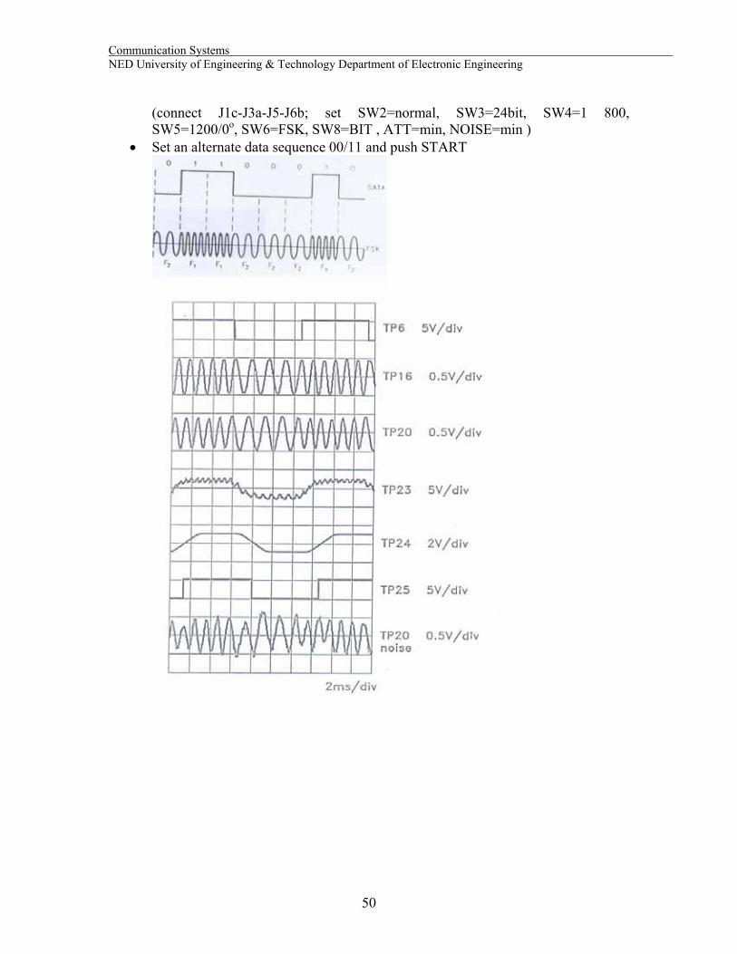
THEORY:- Frequency shift keying -FSK In this modulation the sine carrier takes 2 frequency values, determined by the binary data signal. The modulator can be carried out in different ways among the most used we can mention.
• A voltage controlled oscillator (VCO) • A system transmitting one of the 2 frequencies as function of the data signal. • A frequency divider controlled by the data signal.
The most used demodulation techniques are the one using a PLL circuit. The FSK signal across the PLL input takes two frequency values. The error voltages supplied by the phase comparator follows such variations, and so, it constitutes the NRZ binary representation (high and low level) of the FSK input signal. The PLL demodulator is followed by a low pass filter, which removes the residual carrier components and a squarer circuit which forms the proper data signal. Bit Error rate- B.E.R The B.E.R is the ratio of the error bits to the total received bits. Practically it tells the user how accurate the received data is. BER = (No. of error Bits) / (Total No of received bits) PROCEDURE:- Modulation
• Power the module • Set the circuit in FSK mode, with 24-bit data source and with out data coding
49
Communication Systems NED University of Engineering & Technology Department of Electronic Engineering
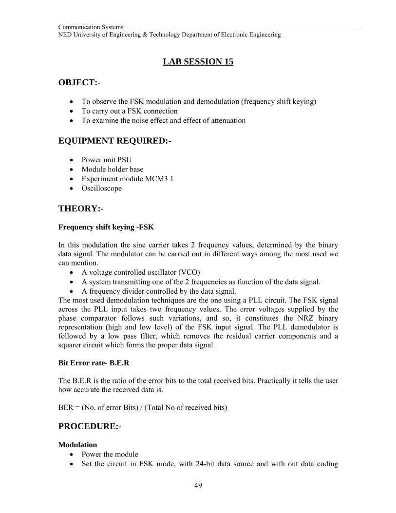
(connect J1c-J3a-J5-J6b; set SW2=normal, SW3=24bit, SW4=1 800, SW5=1200/0o, SW6=FSK, SW8=BIT , ATT=min, NOISE=min )
• Set an alternate data sequence 00/11 and push START
50
Communication Systems NED University of Engineering & Technology Department of Electronic Engineering
51
Communication Systems NED University of Engineering & Technology Department of Electronic Engineering
• Connect the oscilloscope to TP6, TP 14, TP 15, TP16 and examine the data signal
and FSK signal, adjust the phase (PHASE) of the 1200-Hz carrier to get continuity of FSK signal in the passage between the two frequencies (this kind of modulation is known as minimum frequency shift keying)
Demodulation
• Keep the last condition (J1c –J3a-J4-J5-J6b; SW2=Normal ,SW3= 24bit, SW4=1 800, SW=5=1200/00 , SW6=FSK, SW8=BIT , ATT=Min, NOISE =Min
• Set a alternated data sequence 00/11 and push START • Connect the oscilloscope to TP16 and TP20, to examine the FSK signal before
and after the communication channel. Connect oscilloscope to TP23, TP24 and TP29. Note down observations.
• Increase noise & note result then increase attenuation and note result.
Bit Error Rate
• Set the jumpers as follows: J1d-J3d-J4-J5-J6a. • Set Switches as per the following SW2=Normal, SW3=64 bit, SW4=1200Hz,
SW6=ASK, SW8=BIT, SW9=STOP. • Set NOISE at 50 % of maximum value. Set SW9=READ and Push RESET (to
initialize counter to zero). Let the counter progress for 60 seconds after which set SW9=STOP and note counter reading.
• Repeat steps and note error reading for NOISE at 100 %. • The received bits are 18000 per minute. (300 bits/s times 60 seconds).
OBSERVATIONS:-
TP6 ________________________________________________________________ TP14________________________________________________________________ TP15
TP16 ________________________________________________________________
52
Communication Systems NED University of Engineering & Technology Department of Electronic Engineering
TP20 ________________________________________________________________
TP23 ________________________________________________________________
TP24 ________________________________________________________________
TP29
CONCLUSION • Effect of Attenuation
• Effect of Noise • Bit Error Rate readings
At 50 % of maximum Noise
At 100 % Noise
53