precise control of graphene etch ing by remote hydrogen plasma
TRANSCRIPT
ISSN 1998-0124 CN 11-5974/O4
2019, 12(1): 000–000 https://doi.org/10.1007/s12274-018-2192-8
Res
earc
h Ar
ticle
Precise control of graphene etching by remote hydrogen plasma Bangjun Ma1,§, Shizhao Ren1,§, Peiqi Wang1, Chuancheng Jia1, and Xuefeng Guo1,2 ()
1 Beijing National Laboratory for Molecular Sciences, State Key Laboratory for Structural Chemistry of Unstable and Stable Species, College of Chemistry and
Molecular Engineering, Peking University, Beijing 100871, China 2 Department of Materials Science and Engineering, Peking University, Beijing 100871, China § Bangjun Ma and Shizhao Ren contributed equally to this work. © Tsinghua University Press and Springer-Verlag GmbH Germany, part of Springer Nature 2018 Received: 4 December 2017 / Revised: 20 June 2018 / Accepted: 5 September 2018
ABSTRACT Graphene with atomically smooth and configuration-specific edges plays the key role in the performance of graphene-based electronic devices. Remote hydrogen plasma etching of graphene has been proven to be an effective way to create smooth edges with a specific zigzag configuration. However, the etching process is still poorly understood. In this study, with the aid of a custom-made plasma-enhanced hydrogen etching (PEHE) system, a detailed graphene etching process by remote hydrogen plasma is presented. Specifically, we find that hydrogen plasma etching of graphene shows strong thickness and temperature dependence. The etching process of single-layer graphene is isotropic. This is opposite to the anisotropic etching effect observed for bilayer and thicker graphene with an obvious dependence on temperature. On the basis of these observations, a geometrical model was built to illustrate the configuration evolution of graphene edges during etching, which reveals the origin of the anisotropic etching effect. By further utilizing this model, armchair graphene edges were also prepared in a controlled manner for the first time. These investigations offer a better understanding of the etching process for graphene, which should facilitate the fabrication of graphene-based electronic devices with controlled edges and the exploration of more interesting properties of graphene.
KEYWORDS graphene, hydrogen plasma, anisotropic etching, electronic device
1 Introduction The unique electronic structure of graphene makes it an excellent candidate for basic material in future electronic devices. As the lateral dimension of graphene scales down to nanometers, its electrical properties are dominated by the edges because of the localized electronic states of edge atoms [1–6]. In addition, graphene edges are also within the interest of condensed-matter physics, such as energy band engineering and spin-related issues [7–13]. As a remarkable example, graphene nanoribbons have long been predicted to exhibit a certain energy band gap determined by their width and edge configuration [14–18]. Experimental attempts to fabricate graphene nanoribbons with zigzag edges have also demonstrated the existence of edge states through scanning tunneling spectroscopy and even the transition from an antiferromagnetic state (semiconductor) to a ferromagnetic state (metal) at a critical width due to the inversion of spin alignment between the zigzag edges on both sides [19]. Therefore, controlling the configuration of graphene edges is an important issue for the fabrication of graphene-based electronic devices, for example, spintronic devices and semiconducting devices.
In most current approaches to fabricating graphene nanostructures, such as electron beam lithography (EBL) [17] and nanowire-based shadow mask etching [18], the configuration of the resulting graphene edges is randomly formed, as the etching process is too difficult to allow choice. A bottom-up method of surface-assisted chemical synthesis with designed precursors could produce graphene nanoribbons with precisely specified edge configuration, but it requires relatively strict conditions, such as high vacuum and clean metal surfaces, and the synthetic process is difficult to control. Therefore, this
method is not compatible with current device fabrication technologies [16, 20]. Some other chemical approaches with treatments by oxygen, water, and nanoparticles have been reported to produce configuration- specific graphene edges, but the conditions are still too restrictive for the treatments to be used in a practical manner [21–25]. Previous reports have shown that hydrogen plays an important role in the chemical vapor deposition (CVD) growth of graphene on metal substrates, including simultaneous etching and assistive decomposition of carbon species during which the atomic hydrogen from dissociated molecular hydrogen either on the surface of metal substrates or in gaseous phase participate as active species [26–28]. Therefore, it is highly probable that atomic hydrogen could be utilized to etch and modulate graphene edges, considering the fact that it is merely the reverse process of graphene growth from the point of view of the reaction path.
To date, only a few studies have reported on the etching effect of hydrogen on CVD-grown graphene. Regular hexagonal etching pits with a proven zigzag edge configuration were formed on the basal plane of graphene in Refs. [29–31]. There are still other cases where graphene was etched in a fractal pattern [32]. We ascribe these various etching behaviors to the participation of different metal substrates, as they have considerable interaction with graphene, and thus exert a significant impact on the production and diffusion of atomic hydrogen [30, 33]. To avoid the effects of metal substrates and the high temperature required for CVD growth, which restricts the choice of substrates, hydrogen plasma is introduced to directly supply energetic atomic hydrogen and etch graphene on silicon substrates [34]. The active hydrogen species anisotropically etch graphene in a controlled manner to produce atomically smooth edges with a
Address correspondence to [email protected]
Nano Res.
| www.editorialmanager.com/nare/default.asp
2
zigzag configuration [35, 36]. In our opinion, because the etching behaviors are more “intrinsic” for graphene in the absence of metal substrates, remote hydrogen plasma etching might be an optimal method to fabricate graphene nanostructures with well-defined edges when the feasibility, convenience, and compatibility conventional device fabrication technologies are comprehensively considered. However, the detailed etching process is not sufficiently understood, and thus, programmable etching to control the edge configuration of graphene has not been realized to the best of our knowledge. In this work, we elaborate the etching process of graphene by remote hydrogen plasma based on a custom-built plasma-enhanced hydrogen etching (PEHE) system and clarify the etching issue in detail, which provides a better understanding of the etching process and enables the fabrication of a variety of graphene nanostructures with zigzag and other configuration-specific edges.
2 Experimental Graphene sheets were directly prepared by micromechanical cleavage of commercially available Kish graphite onto silicon substrates with a 300 nm thick SiO2 layer, preventing the introduction of possible impurities and other irrelevant factors in the process of growth and transfer of CVD-grown graphene. A simple and effective method, which is described in detail elsewhere [37], was used to rapidly identify the layer number of the graphene sheets based on a standard optical microscope with a charge-coupled device camera. Hydrogen plasma was generated in the upstream part of the PEHE system through an inductively coupled radiofrequency (RF) power supply. The coils were approximately 48 cm away from the center of the furnace to make sure that highly energetic hydrogen ions in the plasma, such as H+, H2
+, and H3+, attenuated adequately, leaving only the less
harsh atomic hydrogen. The etching temperature varied from 300 to 500 °C and the flow of hydrogen was kept at ~ 9.7 sccm (~ 47 Pa). Because the recognizable shape change of straight graphene edges naturally formed by micromechanical cleavage was not exhibited upon etching, circular pits were patterned on the basal plane of graphene by EBL and subsequent reactive ions etching, acting as artificial defects to initialize the etching reaction and make the etching effect apparent enough to be characterized [38, 39].
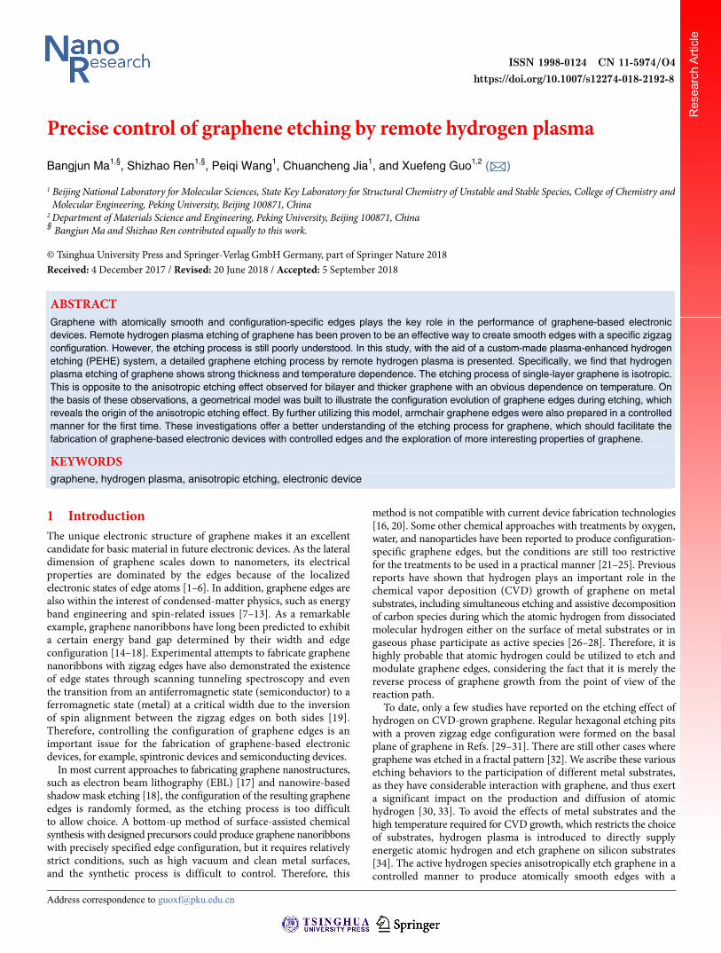
3 Results and discussion The layer dependence of graphene upon remote hydrogen plasma etching was investigated first. For single-layer graphene, the original circular pits with a diameter of about 140 nm expanded in size but preserved their shapes at a RF power of 30 W and temperatures of 320, 420, and 500 °C, shown in Figs. 1(a)–1(c), respectively, an obvious indication of an isotropic etching effect. In addition, newly created circular etching pits with a broad range of diameters were also found randomly distributed on the basal plane of the graphene. The density was the highest at 420 °C. This phenomenon resulted from over-etching because these etching pits were created by the etching reaction and did not originate from either pristine or artificial defects. In contrast, for bilayer and thicker graphene, the circular etching pits were anisotropically transformed to larger hexagonal etching pits with much less over-etching (Figs. 1(d)–1(i)), which is in accordance with a previous report [40]. As the etching time increased, the basal plane of the bilayer graphene showed signs of attack, and newly created hexagonal etching pits gradually appeared when the time reached 1 h (Fig. S1(a) in the Electronic Supplementary Material (ESM)). However, there were no over-etched pits in trilayer graphene under the same etching conditions. To clarify the distinct etching behaviors of single-layer and thicker graphene, additional measurements by Raman spectroscopy and atomic force microscopy (AFM) were carried out. Raman spectra of single-layer graphene after remote hydrogen plasma etching exhibited little
difference from those of pristine and annealed graphene. The small shift of the G and 2D band should be ascribed to the doping effect of the substrate and the atmosphere following the thermal process. A negligible D band was observed for etched graphene because of the newly created defects (Fig. S1(b) in the ESM). Therefore, it can be inferred that graphene kept the sp2-hybridized crystalline lattice without hydrogenation after etching. As seen in the AFM images of trilayer graphene after etching at 420 °C (Figs. S1(c) and S1(d) in the ESM), some single-layer and bilayer deep hexagonal etching pits on the basal plane were found, and all were oriented in the same direction, suggesting simultaneous anisotropic etching reactions at both the edges and the basal planes. When the temperature was raised to 500 °C, over-etching was dramatically suppressed, and no etching pits were found in the trilayer graphene (Fig. S1(e) in the ESM). On the basis of these findings, we propose a so-called bottom-layer passivation model to explain the disparity of the etching effect on single-layer and thicker graphene: Single-layer graphene is so reactive upon remote hydrogen plasma etching because of the surface roughness and charge doping from the silicon substrate that the barriers of etching reactions are easily overcome, eliminating the difference in reactivity between the edges and basal planes, even for the zigzag and armchair crystalline orientations, which leads to an isotropic etching effect and severe over-etching in spite of weak interaction between the graphene and the silicon substrates. For thicker graphene, however, the upper layer of the graphene sheet is isolated from the substrate by the underlying buffer layer and partially passivated, restricting the occurrence of etching to the edge/defect sites, and suppressing the probability of over-etching. As the graphene sheet becomes thicker, the isolation effect becomes stronger, and over-etching on the basal planes is less likely to occur. Now that the effect on the substrate is negligible, the shape of the etching pits is totally determined by the intrinsic crystalline properties of graphene, which is reflected by the anisotropic hexagonal etching pits. According to this model, it is reasonable that even single-layer graphene on the exfoliated hexagonal boron nitride (h-BN) sheet exhibits much less over-etching and an apparent anisotropic etching effect because the flatness and the absence of surface charge on h-BN make it an excellent buffer layer between graphene and silicon substrates [41].
Because single-layer graphene suffers from unavoidable over-etching and isotropic etching effect, and is not suitable for the control of
Figure 1 (a)–(c) SEM images of single-layer graphene after hydrogen plasma etching at an RF power of 30 W and temperatures of 320 °C (30 min), 420 °C (5 min), and 500 °C (5 min), respectively. SEM images of bilayer graphene (d)–(f) and trilayer graphene (g)–(i) after hydrogen plasma etching for 30 min at a RF power of 30 W and temperatures of 320, 420 and 500 °C, respectively. All the scale bars are 500 nm.

Nano Res.
www.theNanoResearch.com∣www.Springer.com/journal/12274 | Nano Research
3
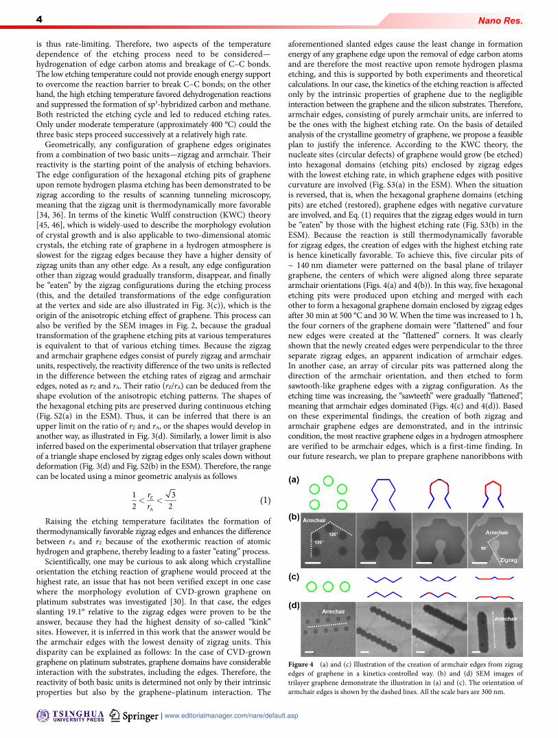
graphene edges, trilayer graphene was chosen for the investigating the temperature dependence of the anisotropic etching effect of graphene, considering the fact that the isolation effect of trilayer graphene is strong enough to withstand over-etching within an acceptable range of etching time. Before that, graphene was patterned with circular pits with a diameter of about 140 nm. At a constant RF power of 30 W and an etching time of 30 min, the furnace temperature was varied from 300 to 500 °C. Interestingly, at 300 °C there seemed to be no obvious shape change in the patterned circular pits, and the hexagonal etching pits were barely recognizable at 320 °C (Figs. 2(a) and 2(b)). Under a longer etching time of 45 min, the hexagonal etching pits were recognizable at 300 °C (Fig. 2(l)), indicating a weak anisotropic etching effect at a relatively low temperature. As the temperature increased, the circular etching pits were transformed to the hexagonal etching pits more and more quickly, and this transformation process was almost undetectable at approximately 420 °C (Figs. 2(c)–2(k)). In addition to the shape evolution, the etching rate, defined as the maximum etched graphene per unit time
along the direction pointing from the center to the vertex of the hexagons, was also estimated from the scanning electron microscopy (SEM) images of the hexagonal etching pits. As shown in Fig. 3(a), the etching rate has a volcano-like relation with the temperature, with a peak located at approximately 400 °C, corresponding to ~ 6 nm/min. According to previous theoretical investigations on the dynamic histogram of atomic hydrogen attack on the graphene crystal lattice [42–44], the etching process can be decomposed into three basic steps (Fig. 3(b)): (1) Hydrogen atoms are chemically adsorbed at the graphene edges with a minimal barrier, and the sp2-hybridized carbon atoms are hydrogenated to become sp3- hybridized, which is energetically favorable; (2) the C–C bonds of neighboring edge carbon atoms are broken by their configuration deformation and the attack of additional energetic hydrogen atoms, resulting in –CH3 and –CH2 groups; (3) the dangling –CH3 groups are unstable and further hydrogenated to form volatile methane, accomplishing a cycle of etching. Of these three steps, the breakage of C–C bonds needs to overcome the largest reaction barrier and
Figure 2 (a)–(k) SEM images of trilayer graphene after etching for 30 min at an RF power of 30 W and 300 °C (a), 320 °C (b), 340 °C (c), 360 °C (d), 380 °C (e), 400 °C(f), 420 °C (g), 440 °C (h), 460 °C (i), 480 °C (j), 500 °C (k). (l) SEM image of trilayer graphene after etching for 45 min at an RF power of 30 W at 300 °C. All the scalebars are 500 nm.
Figure 3 (a) Estimated etching rates for trilayer graphene from the SEM images in Fig. 2. (b) Detailed processes of the etching reaction between hydrogen atoms andzigzag (up)/armchair (down) graphene edges. (c) Illustration of the morphology evolution of graphene edges from circular to hexagonal etching pits. (d) Reactivitydifference between zigzag and armchair graphene edges. The cases noted with “√” were observed experimentally, while those noted with “×” were not, which meansthat the ratio of rZ and rA had to meet the corresponding inequation. The dashed and solid lines represent graphene edges before and after etching. The blue, red andgreen lines represent the direction of zigzag, armchair, and amorphous edges, respectively (similarly hereinafter).
Nano Res.
| www.editorialmanager.com/nare/default.asp
4
is thus rate-limiting. Therefore, two aspects of the temperature dependence of the etching process need to be considered— hydrogenation of edge carbon atoms and breakage of C–C bonds. The low etching temperature could not provide enough energy support to overcome the reaction barrier to break C–C bonds; on the other hand, the high etching temperature favored dehydrogenation reactions and suppressed the formation of sp3-hybridized carbon and methane. Both restricted the etching cycle and led to reduced etching rates. Only under moderate temperature (approximately 400 °C) could the three basic steps proceed successively at a relatively high rate.
Geometrically, any configuration of graphene edges originates from a combination of two basic units—zigzag and armchair. Their reactivity is the starting point of the analysis of etching behaviors. The edge configuration of the hexagonal etching pits of graphene upon remote hydrogen plasma etching has been demonstrated to be zigzag according to the results of scanning tunneling microscopy, meaning that the zigzag unit is thermodynamically more favorable [34, 36]. In terms of the kinetic Wulff construction (KWC) theory [45, 46], which is widely-used to describe the morphology evolution of crystal growth and is also applicable to two-dimensional atomic crystals, the etching rate of graphene in a hydrogen atmosphere is slowest for the zigzag edges because they have a higher density of zigzag units than any other edge. As a result, any edge configuration other than zigzag would gradually transform, disappear, and finally be “eaten” by the zigzag configurations during the etching process (this, and the detailed transformations of the edge configuration at the vertex and side are also illustrated in Fig. 3(c)), which is the origin of the anisotropic etching effect of graphene. This process can also be verified by the SEM images in Fig. 2, because the gradual transformation of the graphene etching pits at various temperatures is equivalent to that of various etching times. Because the zigzag and armchair graphene edges consist of purely zigzag and armchair units, respectively, the reactivity difference of the two units is reflected in the difference between the etching rates of zigzag and armchair edges, noted as rZ and rA. Their ratio (rZ/rA) can be deduced from the shape evolution of the anisotropic etching patterns. The shapes of the hexagonal etching pits are preserved during continuous etching (Fig. S2(a) in the ESM). Thus, it can be inferred that there is an upper limit on the ratio of rZ and rA, or the shapes would develop in another way, as illustrated in Fig. 3(d). Similarly, a lower limit is also inferred based on the experimental observation that trilayer graphene of a triangle shape enclosed by zigzag edges only scales down without deformation (Fig. 3(d) and Fig. S2(b) in the ESM). Therefore, the range can be located using a minor geometric analysis as follows
Z
A
32 2 1 r
r< < (1)
Raising the etching temperature facilitates the formation of thermodynamically favorable zigzag edges and enhances the difference between rA and rZ because of the exothermic reaction of atomic hydrogen and graphene, thereby leading to a faster “eating” process.
Scientifically, one may be curious to ask along which crystalline orientation the etching reaction of graphene would proceed at the highest rate, an issue that has not been verified except in one case where the morphology evolution of CVD-grown graphene on platinum substrates was investigated [30]. In that case, the edges slanting 19.1° relative to the zigzag edges were proven to be the answer, because they had the highest density of so-called “kink” sites. However, it is inferred in this work that the answer would be the armchair edges with the lowest density of zigzag units. This disparity can be explained as follows: In the case of CVD-grown graphene on platinum substrates, graphene domains have considerable interaction with the substrates, including the edges. Therefore, the reactivity of both basic units is determined not only by their intrinsic properties but also by the graphene–platinum interaction. The
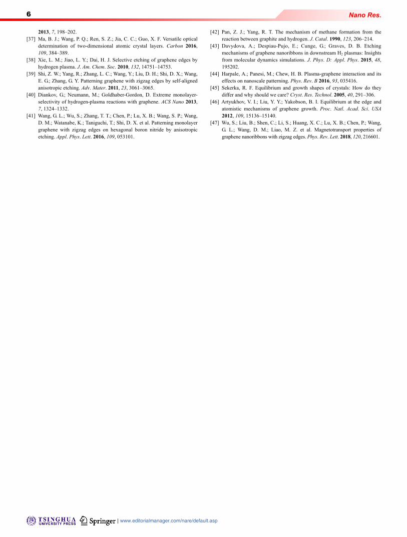
aforementioned slanted edges cause the least change in formation energy of any graphene edge upon the removal of edge carbon atoms and are therefore the most reactive upon remote hydrogen plasma etching, and this is supported by both experiments and theoretical calculations. In our case, the kinetics of the etching reaction is affected only by the intrinsic properties of graphene due to the negligible interaction between the graphene and the silicon substrates. Therefore, armchair edges, consisting of purely armchair units, are inferred to be the ones with the highest etching rate. On the basis of detailed analysis of the crystalline geometry of graphene, we propose a feasible plan to justify the inference. According to the KWC theory, the nucleate sites (circular defects) of graphene would grow (be etched) into hexagonal domains (etching pits) enclosed by zigzag edges with the lowest etching rate, in which graphene edges with positive curvature are involved (Fig. S3(a) in the ESM). When the situation is reversed, that is, when the hexagonal graphene domains (etching pits) are etched (restored), graphene edges with negative curvature are involved, and Eq. (1) requires that the zigzag edges would in turn be “eaten” by those with the highest etching rate (Fig. S3(b) in the ESM). Because the reaction is still thermodynamically favorable for zigzag edges, the creation of edges with the highest etching rate is hence kinetically favorable. To achieve this, five circular pits of ~ 140 nm diameter were patterned on the basal plane of trilayer graphene, the centers of which were aligned along three separate armchair orientations (Figs. 4(a) and 4(b)). In this way, five hexagonal etching pits were produced upon etching and merged with each other to form a hexagonal graphene domain enclosed by zigzag edges after 30 min at 500 °C and 30 W. When the time was increased to 1 h, the four corners of the graphene domain were “flattened” and four new edges were created at the “flattened” corners. It was clearly shown that the newly created edges were perpendicular to the three separate zigzag edges, an apparent indication of armchair edges. In another case, an array of circular pits was patterned along the direction of the armchair orientation, and then etched to form sawtooth-like graphene edges with a zigzag configuration. As the etching time was increasing, the “sawteeth” were gradually “flattened”, meaning that armchair edges dominated (Figs. 4(c) and 4(d)). Based on these experimental findings, the creation of both zigzag and armchair graphene edges are demonstrated, and in the intrinsic condition, the most reactive graphene edges in a hydrogen atmosphere are verified to be armchair edges, which is a first-time finding. In our future research, we plan to prepare graphene nanoribbons with
Figure 4 (a) and (c) Illustration of the creation of armchair edges from zigzag edges of graphene in a kinetics-controlled way. (b) and (d) SEM images of trilayer graphene demonstrate the illustration in (a) and (c). The orientation of armchair edges is shown by the dashed lines. All the scale bars are 300 nm.

Nano Res.
www.theNanoResearch.com∣www.Springer.com/journal/12274 | Nano Research
5
armchair edges to reveal their underlying edge state-related properties [47] (the design can be found in the ESM, Fig. S4).
4 Conclusion In this study, we clarify the hydrogen plasma etching process of graphene by elucidating its layer/temperature dependence, and the edge configuration evolution of graphene. Both zigzag and armchair edges can be created by taking advantage of thermodynamics- controlled and kinetics-controlled reaction paths. These results offer effective guidance for controlling the edge configurations of graphene through remote hydrogen plasma etching, and facilitate the exploration of potentially beneficial graphene nanostructures, pushing forward the application of graphene in electronic devices.
Acknowledgements Financial support from the National Key R&D Program of China (No. 2017YFA0204901) and the National Natural Science Foundation of China (Nos. 21373014 and 21727806) is gratefully acknowledged.
Electronic Supplementary Material: Supplementary material (Raman spectra of pristine, annealed and etched graphene; AFM images of trilayer graphene etched at 420 and 500 °C; SEM image of over- etched bilayer graphene; SEM images of trilayer graphene at varied etching time; schematic illustration of the origin of anisotropic etching effect by remote hydrogen plasma and the design of the fabrication of graphene nanoribbons with armchair edges) is available in the online version of this article at https://doi.org/10.1007/ s12274-018-2192-8.
References [1] Colombo, L.; Wallace, R. M.; Ruoff, R. S. Graphene growth and device
integration. Proc. IEEE 2013, 101, 1536–1556. [2] Das Sarma, S.; Adam, S.; Hwang, E. H.; Rossi, E. Electronic transport in
two-dimensional graphene. Rev. Mod. Phys. 2011, 83, 407–470. [3] Han, M. Y.; Özyilmaz, B.; Zhang, Y. B.; Kim, P. Energy band-gap
engineering of graphene nanoribbons. Phys. Rev. Lett. 2007, 98, 206805. [4] Kim, K.; Choi, J. Y.; Kim, T.; Cho, S. H.; Chung, H. J. A role for graphene
in silicon-based semiconductor devices. Nature 2011, 479, 338–344. [5] Liao, L.; Duan, X. F. Graphene for radio frequency electronics. Mater. Today
2012, 15, 328–338. [6] Novoselov, K. S.; Fal’ko, V. I.; Colombo, L.; Gellert, P. R.; Schwab, M. G.;
Kim, K. A roadmap for graphene. Nature 2012, 490, 192–200. [7] Bai, J. W.; Cheng, R.; Xiu, F. X.; Liao, L.; Wang, M. S.; Shailos, A.; Wang,
K. L.; Huang, Y.; Duan, X. F. Very large magnetoresistance in graphene nanoribbons. Nat. Nanotechnol. 2010, 5, 655–659.
[8] Girit, Ç. Ö.; Meyer, J. C.; Erni, R.; Rossell, M. D.; Kisielowski, C.; Yang, L.; Park, C. H.; Crommie, M. F.; Cohen, M. L.; Louie, S. G. et al. Graphene at the edge: Stability and dynamics. Science 2009, 323, 1705–1708.
[9] Krauss, B.; Nemes-Incze, P.; Skakalova, V.; Biro, L. P.; von Klitzing, K.; Smet, J. H. Raman scattering at pure graphene zigzag edges. Nano Lett. 2010, 10, 4544–4548.
[10] Liu, Y. Y.; Dobrinsky, A.; Yakobson, B. I. Graphene edge from armchair to zigzag: The origins of nanotube chirality? Phys. Rev. Lett. 2010, 105, 235502.
[11] Suenaga, K.; Koshino, M. Atom-by-atom spectroscopy at graphene edge. Nature 2010, 468, 1088–1090.
[12] Tao, C. G.; Jiao, L. Y.; Yazyev, O. V.; Chen, Y. C.; Feng, J. J; Zhang, X. W.; Capaz, R. B.; Tour, J. M.; Zettl, A.; Louie, S. G. et al. Spatially resolving edge states of chiral graphene nanoribbons. Nat. Phys. 2011, 7, 616–620.
[13] Ziatdinov, M.; Fujii, S.; Kusakabe, K.; Kiguchi, M.; Mori, T.; Enoki, T. Visualization of electronic states on atomically smooth graphitic edges with different types of hydrogen termination. Phys. Rev. B 2013, 87, 115427.
[14] Jiao, L. Y.; Zhang, L.; Wang, X. R.; Diankov, G.; Dai, H. J. Narrow graphene nanoribbons from carbon nanotubes. Nature 2009, 458, 877–880.
[15] Li, X. L.; Wang, X. R.; Zhang, L.; Lee, S.; Dai, H. J. Chemically derived, ultrasmooth graphene nanoribbon semiconductors. Science 2008, 319, 1229–1232.
[16] Ruffieux, P.; Wang, S. Y.; Yang, B.; Sánchez-Sánchez, C.; Liu, J.; Dienel, T.; Talirz, L.; Shinde, P.; Pignedoli, C. A.; Passerone, D. et al. On-surface synthesis of graphene nanoribbons with zigzag edge topology. Nature 2016, 531, 489–492.
[17] Wang, X. R.; Ouyang, Y. J.; Li, X. L.; Wang, H. L.; Guo, J.; Dai, H. J. Room-temperature all-semiconducting sub-10-nm graphene nanoribbon field-effect transistors. Phys. Rev. Lett. 2008, 100, 206803.
[18] Yu, W. J.; Duan, X. F. Tunable transport gap in narrow bilayer graphene nanoribbons. Sci. Rep. 2013, 3, 1248.
[19] Magda, G. Z.; Jin, X. Z.; Hagymási, I.; Vancsó, P.; Osváth, Z.; Nemes- Incze, P.; Hwang, C.; Biró, L. P.; Tapasztó, L. Room-temperature magnetic order on zigzag edges of narrow graphene nanoribbons. Nature 2014, 514, 608–611.
[20] Cai, J.; Ruffieux, P.; Jaafar, R.; Bieri, M.; Braun, T.; Blankenburg, S.; Muoth, M.; Seitsonen, A. P.; Saleh, M.; Feng, X.; Mullen, K.; Fasel, R. Atomically precise bottom-up fabrication of graphene nanoribbons. Nature 2010, 466, 470–473.
[21] Dobrik, G.; Tapasztó, L.; Biró, L. P. Selective etching of armchair edges in graphite. Carbon 2013, 56, 332–338.
[22] Luo, D.; Yang, F.; Wang, X.; Sun, H.; Gao, D. L.; Li, R. M.; Yang, J.; Li, Y. Anisotropic etching of graphite flakes with water vapor to produce armchair-edged graphene. Small 2014, 10, 2809–2814.
[23] Campos, L. C.; Manfrinato, V. R.; Sanchez-Yamagishi, J. D.; Kong, J.; Jarillo-Herrero, P. Anisotropic etching and nanoribbon formation in single-layer graphene. Nano Lett. 2009, 9, 2600–2604.
[24] Nemes-Incze, P.; Magda, G.; Kamarás, K.; Biró, L. P. Crystallographically selective nanopatterning of graphene on SiO2. Nano Res. 2010, 3, 110–116.
[25] Ci, L. J.; Xu, Z. P.; Wang, L. L.; Gao, W.; Ding, F.; Kelly, K. F.; Yakobson, B. I.; Ajayan, P. M. Controlled nanocutting of graphene. Nano Res. 2008, 1, 116–122.
[26] Qi, M.; Ren, Z. Y.; Jiao, Y.; Zhou, Y. X.; Xu, X. L.; Li, W. L.; Li, J. Y.; Zheng, X. L.; Bai, J. T. Hydrogen kinetics on scalable graphene growth by atmospheric pressure chemical vapor deposition with acetylene. J. Phys. Chem. C 2013, 117, 14348–14353.
[27] Vlassiouk, I.; Regmi, M.; Fulvio, P.; Dai, S.; Datskos, P.; Eres, G.; Smirnov, S. Role of hydrogen in chemical vapor deposition growth of large single-crystal graphene. ACS Nano 2011, 5, 6069–6076.
[28] Zhang, X. Y.; Wang, L.; Xin, J.; Yakobson, B. I.; Ding, F. Role of hydrogen in graphene chemical vapor deposition growth on a copper surface. J. Am. Chem. Soc. 2014, 136, 3040–3047.
[29] Zhang, Y.; Li, Z.; Kim, P.; Zhang, L.; Zhou, C. W. Anisotropic hydrogen etching of chemical vapor deposited graphene. ACS Nano 2012, 6, 126–132.
[30] Ma, T.; Ren, W. C.; Zhang, X. Y.; Liu, Z. B.; Gao, Y.; Yin, L. C.; Ma, X. L.; Ding, F.; Cheng, H. M. Edge-controlled growth and kinetics of single- crystal graphene domains by chemical vapor deposition. Proc. Natl. Acad. Sci. USA 2013, 110, 20386–20391.
[31] Zhang, H. R.; Zhang, Y. H.; Zhang, Y. Q.; Chen, Z. Y.; Sui, Y. P.; Ge, X. M.; Yu, G. H.; Jin, Z.; Liu, X. Y. Edge morphology evolution of graphene domains during chemical vapor deposition cooling revealed through hydrogen etching. Nanoscale 2016, 8, 4145–4150.
[32] Geng, D. C.; Wu, B.; Guo, Y. L.; Luo, B. R.; Xue, Y. Z.; Chen, J. Y.; Yu, G.; Liu, Y. Q. Fractal etching of graphene. J. Am. Chem. Soc. 2013, 135, 6431–6434.
[33] Knox, K. R.; Wang, S. C.; Morgante, A.; Cvetko, D.; Locatelli, A.; Mentes, T. O.; Niño, M. A.; Kim, P.; Osgood, R. M. Jr. Spectromicroscopy of single and multilayer graphene supported by a weakly interacting substrate. Phys. Rev. B 2008, 78, 201408(R).
[34] Yang, R.; Zhang, L. C.; Wang, Y.; Shi, Z. W.; Shi, D. X.; Gao, H. J.; Wang, E. G.; Zhang, G. Y. An anisotropic etching effect in the graphene basal plane. Adv. Mater. 2010, 22, 4014–4019.
[35] Guo, Y. F.; Guo, W. L. Favorable zigzag configuration at etched graphene edges. J. Phys. Chem. C 2011, 115, 20546–20549.
[36] Zhang, X. W.; Yazyev, O. V.; Feng, J. J.; Xie, L. M.; Tao, C. G.; Chen, Y. C.; Jiao, L. Y.; Pedramrazi, Z.; Zettl, A.; Louie, S. G. et al. Experimentally engineering the edge termination of graphene nanoribbons. ACS Nano
Nano Res.
| www.editorialmanager.com/nare/default.asp
6
2013, 7, 198–202. [37] Ma, B. J.; Wang, P. Q.; Ren, S. Z.; Jia, C. C.; Guo, X. F. Versatile optical
determination of two-dimensional atomic crystal layers. Carbon 2016, 109, 384–389.
[38] Xie, L. M.; Jiao, L. Y.; Dai, H. J. Selective etching of graphene edges by hydrogen plasma. J. Am. Chem. Soc. 2010, 132, 14751–14753.
[39] Shi, Z. W.; Yang, R.; Zhang, L. C.; Wang, Y.; Liu, D. H.; Shi, D. X.; Wang, E. G.; Zhang, G. Y. Patterning graphene with zigzag edges by self-aligned anisotropic etching. Adv. Mater. 2011, 23, 3061–3065.
[40] Diankov, G.; Neumann, M.; Goldhaber-Gordon, D. Extreme monolayer- selectivity of hydrogen-plasma reactions with graphene. ACS Nano 2013, 7, 1324–1332.
[41] Wang, G. L.; Wu, S.; Zhang, T. T.; Chen, P.; Lu, X. B.; Wang, S. P.; Wang, D. M.; Watanabe, K.; Taniguchi, T.; Shi, D. X. et al. Patterning monolayer graphene with zigzag edges on hexagonal boron nitride by anisotropic etching. Appl. Phys. Lett. 2016, 109, 053101.
[42] Pan, Z. J.; Yang, R. T. The mechanism of methane formation from the reaction between graphite and hydrogen. J. Catal. 1990, 123, 206–214.
[43] Davydova, A.; Despiau-Pujo, E.; Cunge, G.; Graves, D. B. Etching mechanisms of graphene nanoribbons in downstream H2 plasmas: Insights from molecular dynamics simulations. J. Phys. D: Appl. Phys. 2015, 48, 195202.
[44] Harpale, A.; Panesi, M.; Chew, H. B. Plasma-graphene interaction and its effects on nanoscale patterning. Phys. Rev. B 2016, 93, 035416.
[45] Sekerka, R. F. Equilibrium and growth shapes of crystals: How do they differ and why should we care? Cryst. Res. Technol. 2005, 40, 291–306.
[46] Artyukhov, V. I.; Liu, Y. Y.; Yakobson, B. I. Equilibrium at the edge and atomistic mechanisms of graphene growth. Proc. Natl. Acad. Sci. USA 2012, 109, 15136–15140.
[47] Wu, S.; Liu, B.; Shen, C.; Li, S.; Huang, X. C.; Lu, X. B.; Chen, P.; Wang, G. L.; Wang, D. M.; Liao, M. Z. et al. Magnetotransport properties of graphene nanoribbons with zigzag edges. Phys. Rev. Lett. 2018, 120, 216601.