precision instrumentation amplifier with signal …...precision instrumentation amplifier with...
TRANSCRIPT
Precision Instrumentation Amplifierwith Signal Processing Amplifiers
AD8295
Rev. A Information furnished by Analog Devices is believed to be accurate and reliable. However, no responsibility is assumed by Analog Devices for its use, nor for any infringements of patents or other rights of third parties that may result from its use. Specifications subject to change without notice. No license is granted by implication or otherwise under any patent or patent rights of Analog Devices. Trademarks and registered trademarks are the property of their respective owners.
One Technology Way, P.O. Box 9106, Norwood, MA 02062-9106, U.S.A.Tel: 781.329.4700 www.analog.com Fax: 781.461.3113 ©2008–2009 Analog Devices, Inc. All rights reserved.
FEATURES Saves board space Includes precision in-amp, 2 op amps, and
2 matched resistors 4 mm × 4 mm LFCSP
No heat slug for more routing room Differential output fully specified In-amp specifications
Gain set with 1 external resistor (gain range: 1 to 1000) Input voltage noise: 8 nV/√Hz maximum at 1 kHz CMRR (G = 1): 90 dB minimum Input bias current: 0.8 nA maximum −3 dB bandwidth (G = 1): 1.2 MHz Slew rate: 2 V/μs
Wide power supply range: ±2.3 V to ±18 V 1 ppm/°C, 0.03% resistor matching
APPLICATIONS Industrial process controls Wheatstone bridges Precision data acquisition systems Medical instrumentation Strain gages Transducer interfaces Differential output
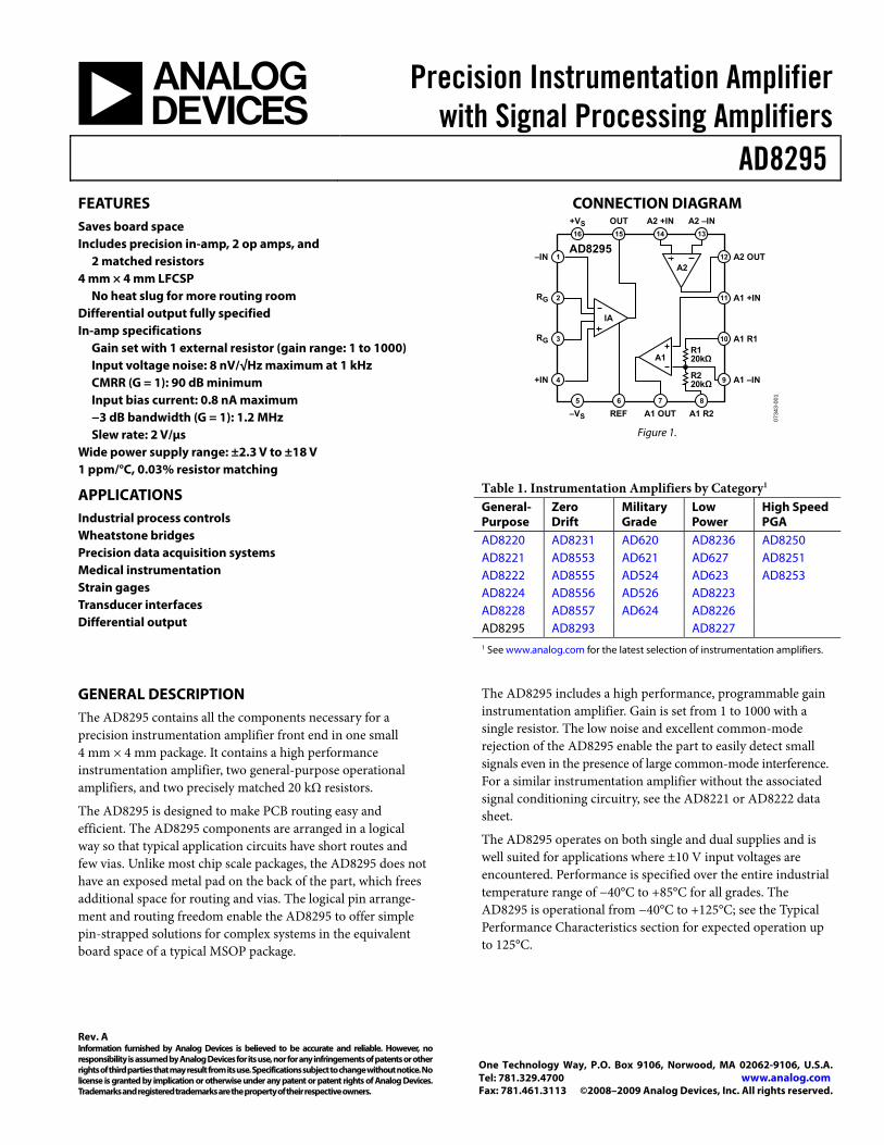
CONNECTION DIAGRAM
A1 OUT A1 R2
A2 +IN A2 –IN
–IN
RG
+VS
–VS
OUT
REF
RG
+IN
16 15 14 13
1
2
3
4
8765
A1
IA
A2
R120kΩ
R220kΩ
A2 OUTAD8295
A1 +IN
A1 R1
A1 –IN
12
11
10
9
0734
3-00
1
Figure 1.
Table 1. Instrumentation Amplifiers by Category1 General- Purpose
Zero Drift
Military Grade
Low Power
High Speed PGA
AD8220 AD8231 AD620 AD8236 AD8250AD8221 AD8553 AD621 AD627 AD8251AD8222 AD8555 AD524 AD623 AD8253AD8224 AD8556 AD526 AD8223 AD8228 AD8557 AD624 AD8226 AD8295 AD8293 AD8227 1 See www.analog.com for the latest selection of instrumentation amplifiers.
GENERAL DESCRIPTION The AD8295 contains all the components necessary for a precision instrumentation amplifier front end in one small 4 mm × 4 mm package. It contains a high performance instrumentation amplifier, two general-purpose operational amplifiers, and two precisely matched 20 kΩ resistors.
The AD8295 is designed to make PCB routing easy and efficient. The AD8295 components are arranged in a logical way so that typical application circuits have short routes and few vias. Unlike most chip scale packages, the AD8295 does not have an exposed metal pad on the back of the part, which frees additional space for routing and vias. The logical pin arrange-ment and routing freedom enable the AD8295 to offer simple pin-strapped solutions for complex systems in the equivalent board space of a typical MSOP package.
The AD8295 includes a high performance, programmable gain instrumentation amplifier. Gain is set from 1 to 1000 with a single resistor. The low noise and excellent common-mode rejection of the AD8295 enable the part to easily detect small signals even in the presence of large common-mode interference. For a similar instrumentation amplifier without the associated signal conditioning circuitry, see the AD8221 or AD8222 data sheet.
The AD8295 operates on both single and dual supplies and is well suited for applications where ±10 V input voltages are encountered. Performance is specified over the entire industrial temperature range of −40°C to +85°C for all grades. The AD8295 is operational from −40°C to +125°C; see the Typical Performance Characteristics section for expected operation up to 125°C.
AD8295
Rev. A | Page 2 of 28
TABLE OF CONTENTS Features .............................................................................................. 1
Applications ....................................................................................... 1
Connection Diagram ....................................................................... 1
General Description ......................................................................... 1
Revision History ............................................................................... 2
Specifications ..................................................................................... 3
Instrumentation Amplifier Specifications, Single-Ended and Differential Output Configurations ........................................... 3
Op Amp Specifications ................................................................ 5
Internal Resistor Network ........................................................... 6
Power and Temperature Specifications ..................................... 6
Absolute Maximum Ratings ............................................................ 7
Thermal Characteristics .............................................................. 7
ESD Caution .................................................................................. 7
Pin Configuration and Function Descriptions ............................. 8
Typical Performance Characteristics ............................................. 9
In-Amp .......................................................................................... 9
Op Amps ...................................................................................... 16
System .......................................................................................... 18
Theory of Operation ...................................................................... 19
Uncommitted Op Amps ............................................................ 19
Instrumentation Amplifier........................................................ 19
Layout .......................................................................................... 20
Input Protection ......................................................................... 21
Input Bias Current Return Path ............................................... 21
RF Interference ........................................................................... 21
Differential Output .................................................................... 22
Applications Information .............................................................. 23
Creating a Reference Voltage at Midscale ............................... 23
High Accuracy G = −1 Configuration with Low-Pass Filter .. 23
Two-Pole Sallen-Key Filter ........................................................ 24
AC-Coupled Instrumentation Amplifier ................................ 24
Driving Differential ADCs ........................................................ 25
Outline Dimensions ....................................................................... 26
Ordering Guide .......................................................................... 26
REVISION HISTORY 6/09—Rev. 0 to Rev. A
Changes to General Description Section ...................................... 1 Changes to Table 1 ............................................................................ 1 Changes to Table 3 ............................................................................ 5 Added Figure 42, Figure 45, and Figure 46; Renumbered Sequentially ..................................................................................... 16 Added Figure 49 .............................................................................. 17 Changes to Figure 51 and Figure 52 ............................................. 17 Added Figure 53 and Figure 54..................................................... 18 Changes to Figure 59 ...................................................................... 19 Added Routing and Vias Section .................................................. 20 Updated Outline Dimensions ....................................................... 26
10/08—Revision 0: Initial Version
AD8295
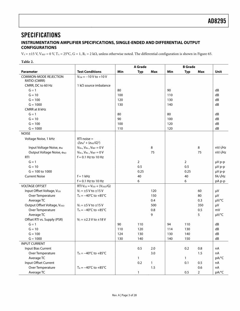
Rev. A | Page 3 of 28
SPECIFICATIONS INSTRUMENTATION AMPLIFIER SPECIFICATIONS, SINGLE-ENDED AND DIFFERENTIAL OUTPUT CONFIGURATIONS VS = ±15 V, VREF = 0 V, TA = 25°C, G = 1, RL = 2 kΩ, unless otherwise noted. The differential configuration is shown in Figure 65.
Table 2. A Grade B Grade Parameter Test Conditions Min Typ Max Min Typ Max Unit COMMON-MODE REJECTION
RATIO (CMRR) VCM = −10 V to +10 V
CMRR, DC to 60 Hz 1 kΩ source imbalance G = 1 80 90 dB G = 10 100 110 dB G = 100 120 130 dB G = 1000 130 140 dB
CMRR at 8 kHz G = 1 80 80 dB G = 10 90 100 dB G = 100 100 120 dB G = 1000 110 120 dB
NOISE
Voltage Noise, 1 kHz RTI noise = √(eNI
2 + (eNO/G)2)
Input Voltage Noise, eNI VIN+, VIN−, VREF = 0 V 8 8 nV/√Hz Output Voltage Noise, eNO VIN+, VIN−, VREF = 0 V 75 75 nV/√Hz
RTI f = 0.1 Hz to 10 Hz G = 1 2 2 μV p-p G = 10 0.5 0.5 μV p-p G = 100 to 1000 0.25 0.25 μV p-p
Current Noise f = 1 kHz 40 40 fA/√Hz f = 0.1 Hz to 10 Hz 6 6 pA p-p
VOLTAGE OFFSET RTI VOS = VOSI + (VOSO/G) Input Offset Voltage, VOSI VS = ±5 V to ±15 V 120 60 μV
Over Temperature TA = −40°C to +85°C 150 80 μV Average TC 0.4 0.3 μV/°C
Output Offset Voltage, VOSO VS = ±5 V to ±15 V 500 350 μV Over Temperature TA = −40°C to +85°C 0.8 0.5 mV Average TC 9 5 μV/°C
Offset RTI vs. Supply (PSR) VS = ±2.3 V to ±18 V G = 1 90 110 94 110 dB G = 10 110 120 114 130 dB G = 100 124 130 130 140 dB G = 1000 130 140 140 150 dB
INPUT CURRENT Input Bias Current 0.5 2.0 0.2 0.8 nA
Over Temperature TA = −40°C to +85°C 3.0 1.5 nA Average TC 1 1 pA/°C
Input Offset Current 0.2 1 0.1 0.5 nA Over Temperature TA = −40°C to +85°C 1.5 0.6 nA Average TC 1 0.5 2 pA/°C
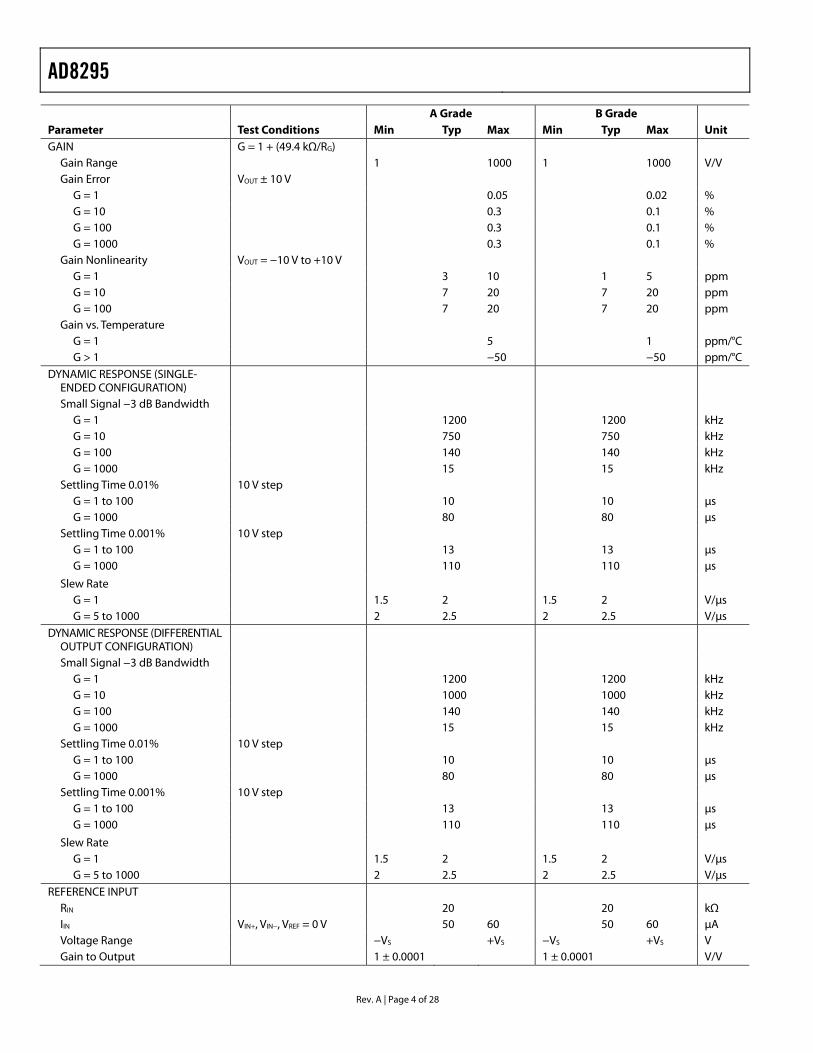
AD8295
Rev. A | Page 4 of 28
A Grade B Grade Parameter Test Conditions Min Typ Max Min Typ Max Unit GAIN G = 1 + (49.4 kΩ/RG)
Gain Range 1 1000 1 1000 V/V Gain Error VOUT ± 10 V
G = 1 0.05 0.02 % G = 10 0.3 0.1 % G = 100 0.3 0.1 % G = 1000 0.3 0.1 %
Gain Nonlinearity VOUT = −10 V to +10 V G = 1 3 10 1 5 ppm G = 10 7 20 7 20 ppm G = 100 7 20 7 20 ppm
Gain vs. Temperature G = 1 5 1 ppm/°C G > 1 −50 −50 ppm/°C
DYNAMIC RESPONSE (SINGLE-ENDED CONFIGURATION)
Small Signal −3 dB Bandwidth G = 1 1200 1200 kHz G = 10 750 750 kHz G = 100 140 140 kHz G = 1000 15 15 kHz
Settling Time 0.01% 10 V step G = 1 to 100 10 10 μs G = 1000 80 80 μs
Settling Time 0.001% 10 V step G = 1 to 100 13 13 μs G = 1000 110 110 μs
Slew Rate G = 1 1.5 2 1.5 2 V/μs G = 5 to 1000 2 2.5 2 2.5 V/μs
DYNAMIC RESPONSE (DIFFERENTIAL OUTPUT CONFIGURATION)
Small Signal −3 dB Bandwidth G = 1 1200 1200 kHz G = 10 1000 1000 kHz G = 100 140 140 kHz G = 1000 15 15 kHz
Settling Time 0.01% 10 V step G = 1 to 100 10 10 μs G = 1000 80 80 μs
Settling Time 0.001% 10 V step G = 1 to 100 13 13 μs G = 1000 110 110 μs
Slew Rate G = 1 1.5 2 1.5 2 V/μs G = 5 to 1000 2 2.5 2 2.5 V/μs
REFERENCE INPUT RIN 20 20 kΩ IIN VIN+, VIN−, VREF = 0 V 50 60 50 60 μA Voltage Range −VS +VS −VS +VS V Gain to Output 1 ± 0.0001 1 ± 0.0001 V/V
AD8295
Rev. A | Page 5 of 28
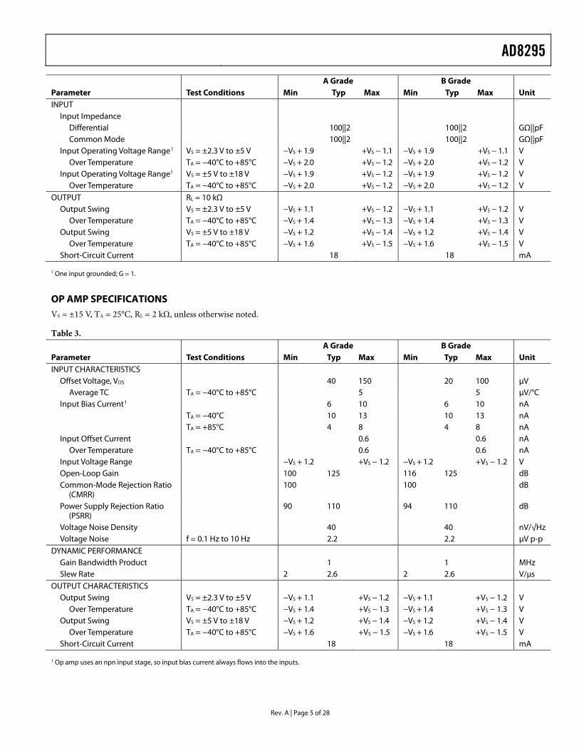
A Grade B Grade Parameter Test Conditions Min Typ Max Min Typ Max Unit INPUT
Input Impedance Differential 100||2 100||2 GΩ||pF Common Mode 100||2 100||2 GΩ||pF
Input Operating Voltage Range1 VS = ±2.3 V to ±5 V −VS + 1.9 +VS − 1.1 −VS + 1.9 +VS − 1.1 V
Over Temperature TA = −40°C to +85°C −VS + 2.0 +VS − 1.2 −VS + 2.0 +VS − 1.2 V Input Operating Voltage Range1
VS = ±5 V to ±18 V −VS + 1.9 +VS − 1.2 −VS + 1.9 +VS − 1.2 V Over Temperature TA = −40°C to +85°C −VS + 2.0 +VS − 1.2 −VS + 2.0 +VS − 1.2 V
OUTPUT RL = 10 kΩ Output Swing VS = ±2.3 V to ±5 V −VS + 1.1 +VS − 1.2 −VS + 1.1 +VS − 1.2 V
Over Temperature TA = −40°C to +85°C −VS + 1.4 +VS − 1.3 −VS + 1.4 +VS − 1.3 V Output Swing VS = ±5 V to ±18 V −VS + 1.2 +VS − 1.4 −VS + 1.2 +VS − 1.4 V
Over Temperature TA = −40°C to +85°C −VS + 1.6 +VS − 1.5 −VS + 1.6 +VS − 1.5 V Short-Circuit Current 18 18 mA
1 One input grounded; G = 1.
OP AMP SPECIFICATIONS VS = ±15 V, TA = 25°C, RL = 2 kΩ, unless otherwise noted.
Table 3. A Grade B Grade Parameter Test Conditions Min Typ Max Min Typ Max Unit INPUT CHARACTERISTICS
Offset Voltage, VOS 40 150 20 100 μV Average TC TA = −40°C to +85°C 5 5 μV/°C
Input Bias Current1 6 10 6 10 nA
TA = −40°C 10 13 10 13 nA TA = +85°C 4 8 4 8 nA
Input Offset Current 0.6 0.6 nA Over Temperature TA = −40°C to +85°C 0.6 0.6 nA
Input Voltage Range −VS + 1.2 +VS − 1.2 −VS + 1.2 +VS − 1.2 V Open-Loop Gain 100 125 116 125 dB Common-Mode Rejection Ratio
(CMRR) 100 100 dB
Power Supply Rejection Ratio (PSRR)
90 110 94 110 dB
Voltage Noise Density 40 40 nV/√Hz Voltage Noise f = 0.1 Hz to 10 Hz 2.2 2.2 μV p-p
DYNAMIC PERFORMANCE Gain Bandwidth Product 1 1 MHz Slew Rate 2 2.6 2 2.6 V/μs
OUTPUT CHARACTERISTICS Output Swing VS = ±2.3 V to ±5 V −VS + 1.1 +VS − 1.2 −VS + 1.1 +VS − 1.2 V
Over Temperature TA = −40°C to +85°C −VS + 1.4 +VS − 1.3 −VS + 1.4 +VS − 1.3 V Output Swing VS = ±5 V to ±18 V −VS + 1.2 +VS − 1.4 −VS + 1.2 +VS − 1.4 V
Over Temperature TA = −40°C to +85°C −VS + 1.6 +VS − 1.5 −VS + 1.6 +VS − 1.5 V Short-Circuit Current 18 18 mA
1 Op amp uses an npn input stage, so input bias current always flows into the inputs.
AD8295
Rev. A | Page 6 of 28
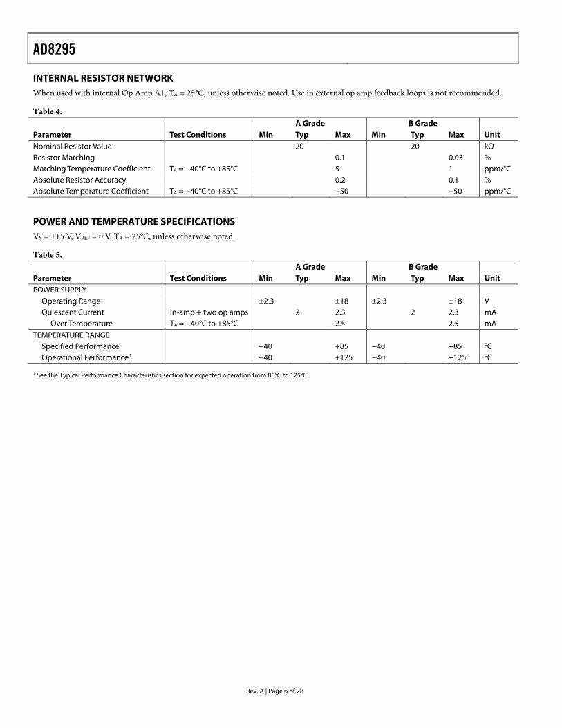
INTERNAL RESISTOR NETWORK When used with internal Op Amp A1, TA = 25°C, unless otherwise noted. Use in external op amp feedback loops is not recommended.
Table 4. A Grade B Grade Parameter Test Conditions Min Typ Max Min Typ Max Unit Nominal Resistor Value 20 20 kΩ Resistor Matching 0.1 0.03 % Matching Temperature Coefficient TA = −40°C to +85°C 5 1 ppm/°C Absolute Resistor Accuracy 0.2 0.1 % Absolute Temperature Coefficient TA = −40°C to +85°C −50 −50 ppm/°C
POWER AND TEMPERATURE SPECIFICATIONS VS = ±15 V, VREF = 0 V, TA = 25°C, unless otherwise noted.
Table 5. A Grade B Grade Parameter Test Conditions Min Typ Max Min Typ Max Unit POWER SUPPLY
Operating Range ±2.3 ±18 ±2.3 ±18 V Quiescent Current In-amp + two op amps 2 2.3 2 2.3 mA
Over Temperature TA = −40°C to +85°C 2.5 2.5 mA TEMPERATURE RANGE
Specified Performance −40 +85 −40 +85 °C Operational Performance1
−40 +125 −40 +125 °C 1 See the section for expected operation from 85°C to 125°C. Typical Performance Characteristics
AD8295
Rev. A | Page 7 of 28
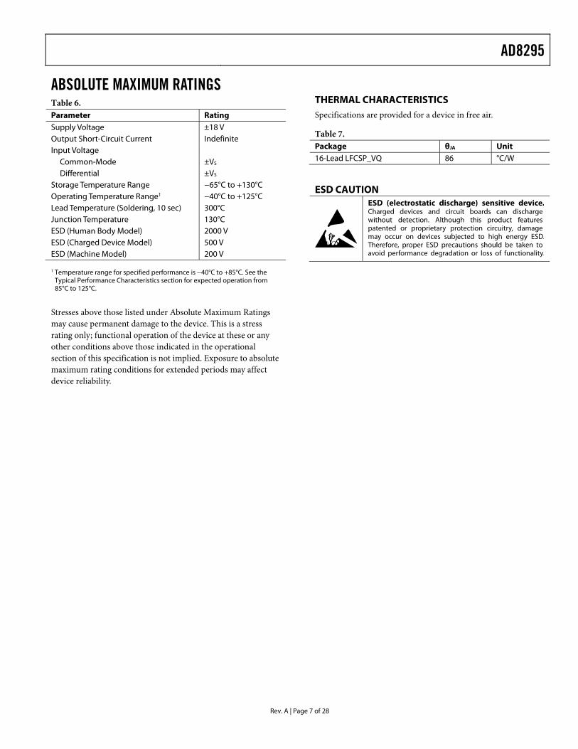
ABSOLUTE MAXIMUM RATINGS Table 6. Parameter Rating Supply Voltage ±18 V Output Short-Circuit Current Indefinite Input Voltage
Common-Mode ±VS Differential ±VS
Storage Temperature Range −65°C to +130°C Operating Temperature Range1 −40°C to +125°C Lead Temperature (Soldering, 10 sec) 300°C Junction Temperature 130°C ESD (Human Body Model) 2000 V ESD (Charged Device Model) 500 V ESD (Machine Model) 200 V 1 Temperature range for specified performance is −40°C to +85°C. See the
Typical Performance Characteristics section for expected operation from 85°C to 125°C.
Stresses above those listed under Absolute Maximum Ratings may cause permanent damage to the device. This is a stress rating only; functional operation of the device at these or any other conditions above those indicated in the operational section of this specification is not implied. Exposure to absolute maximum rating conditions for extended periods may affect device reliability.
THERMAL CHARACTERISTICS Specifications are provided for a device in free air.
Table 7. Package θJA Unit 16-Lead LFCSP_VQ 86 °C/W
ESD CAUTION
AD8295
Rev. A | Page 8 of 28
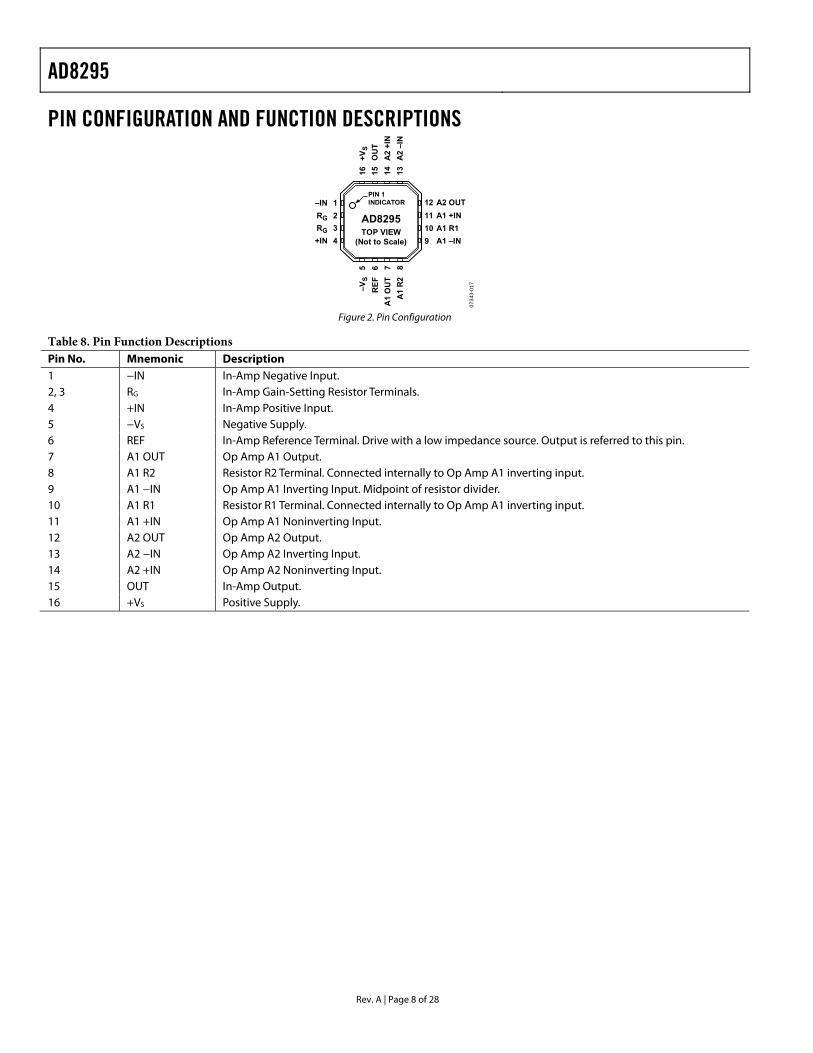
PIN CONFIGURATION AND FUNCTION DESCRIPTIONS
0734
3-01
7
5–V
S6
REF
7A
1 O
UT
8A
1 R
2
PIN 1INDICATOR1–IN
2RG3RG4+IN
11 A1 +IN12 A2 OUT
10 A1 R19 A1 –IN
15O
UT
16+V
S
14A
2 +I
N13
A2
–IN
TOP VIEW(Not to Scale)
AD8295
Figure 2. Pin Configuration
Table 8. Pin Function Descriptions Pin No. Mnemonic Description 1 −IN In-Amp Negative Input. 2, 3 RG In-Amp Gain-Setting Resistor Terminals. 4 +IN In-Amp Positive Input. 5 −VS Negative Supply. 6 REF In-Amp Reference Terminal. Drive with a low impedance source. Output is referred to this pin. 7 A1 OUT Op Amp A1 Output. 8 A1 R2 Resistor R2 Terminal. Connected internally to Op Amp A1 inverting input. 9 A1 −IN Op Amp A1 Inverting Input. Midpoint of resistor divider. 10 A1 R1 Resistor R1 Terminal. Connected internally to Op Amp A1 inverting input. 11 A1 +IN Op Amp A1 Noninverting Input. 12 A2 OUT Op Amp A2 Output. 13 A2 −IN Op Amp A2 Inverting Input. 14 A2 +IN Op Amp A2 Noninverting Input. 15 OUT In-Amp Output. 16 +VS Positive Supply.
AD8295
Rev. A | Page 9 of 28
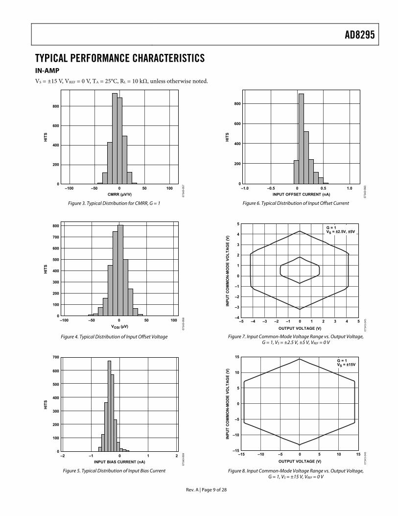
0–100 –50 0 50 100
CMRR (µV/V)
TYPICAL PERFORMANCE CHARACTERISTICS IN-AMP VS = ±15 V, VREF = 0 V, TA = 25°C, RL = 10 kΩ, unless otherwise noted.
800
600
400
200
HIT
S
0734
3-05
7
0–100 –50 0 50 100
VOSI (µV)
Figure 3. Typical Distribution for CMRR, G = 1
800
700
600
500
400
300
200
100
HIT
S
0734
3-05
8
0–2 –1 0 1 2
INPUT BIAS CURRENT (nA)
Figure 4. Typical Distribution of Input Offset Voltage
600
700
500
400
300
200
100
HIT
S
0734
3-05
9
800
600
400
200
0–1.0 –0.5 0 0.5 1.0
HIT
S
INPUT OFFSET CURRENT (nA)
Figure 5. Typical Distribution of Input Bias Current
0734
3-06
0
Figure 6. Typical Distribution of Input Offset Current
–4
–3
–2
–1
0
1
2
3
4
5
–5 –4 –3 –2 –1 0 1 2 3 4 5
0734
3-04
5
OUTPUT VOLTAGE (V)
INPU
T C
OM
MO
N-M
OD
E VO
LTA
GE
(V)
G = 1VS = ±2.5V, ±5V
Figure 7. Input Common-Mode Voltage Range vs. Output Voltage, G = 1, VS = ±2.5 V, ±5 V, VREF = 0 V
–15
–10
–5
0
5
10
15
–15 –10 –5 0 5 10 15
3-04
6
INPU
T C
OM
MO
N-M
OD
E VO
LTA
GE
(V)
G = 1VS = ±15V
0734OUTPUT VOLTAGE (V)
Figure 8. Input Common-Mode Voltage Range vs. Output Voltage, G = 1, VS = ±15 V, VREF = 0 V
AD8295
Rev. A | Page 10 of 28
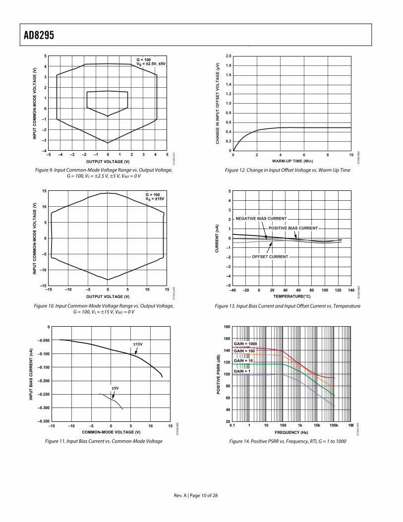
–4
–3
–5 –4 –3 –2 –1 0 1 2 3 4 5
3-04
7
INPU
T C
OM
MO
N-M
OD
E VO
LTA
GE
(V)
–2
–1
0
1
2
3
4
5
0734OUTPUT VOLTAGE (V)
G = 100VS = ±2.5V, ±5V
Figure 9. Input Common-Mode Voltage Range vs. Output Voltage, G = 100, VS = ±2.5 V, ±5 V, VREF = 0 V
–15–15 –10 –5 0 5 10 15
3-04
8
INPU
T C
OM
MO
N-M
OD
E VO
LTA
GE
(V)
–10
–5
0
5
10
15
0734OUTPUT VOLTAGE (V)
G = 100VS = ±15V
–0.350–15 –10 –5 0 5 10 15
COMMON-MODE VOLTAGE (V)
Figure 10. Input Common-Mode Voltage Range vs. Output Voltage, G = 100, VS = ±15 V, VREF = 0 V
0
–0.050
–0.100
–0.150
–0.200
–0.250
–0.300
INPU
T B
IAS
CU
RR
ENT
(nA
)
±15V
±5V
0734
3-06
1
2.0
0
0.2
0.4
0.6
0.8
1.0
1.2
1.4
1.6
1.8
0 2 4 6 8 10WARM-UP TIME (Min)
CH
AN
GE
IN IN
PUT
OFF
SET
VOLT
AG
E (µ
V)
Figure 11. Input Bias Current vs. Common-Mode Voltage
0734
3-06
2
5
4
3
2
1
0
–1
–2
–3
–4
–5–40 –20 0 20 40 60 80 100 120 140
CU
RR
ENT
(nA
)
TEMPERATURE(°C)
Figure 12. Change in Input Offset Voltage vs. Warm-Up Time
POSITIVE BIAS CURRENT
NEGATIVE BIAS CURRENT
OFFSET CURRENT
0734
3-06
3
Figure 13. Input Bias Current and Input Offset Current vs. Temperature
200.1 1 10 100 1k 10k 100k 1M
0734
3-04
9
FREQUENCY (Hz)
40
60
80
100
120
140
160
180
POSI
TIVE
PSR
R (d
B)
GAIN = 1000
GAIN = 100
GAIN = 10
GAIN = 1
Figure 14. Positive PSRR vs. Frequency, RTI, G = 1 to 1000
AD8295
Rev. A | Page 11 of 28
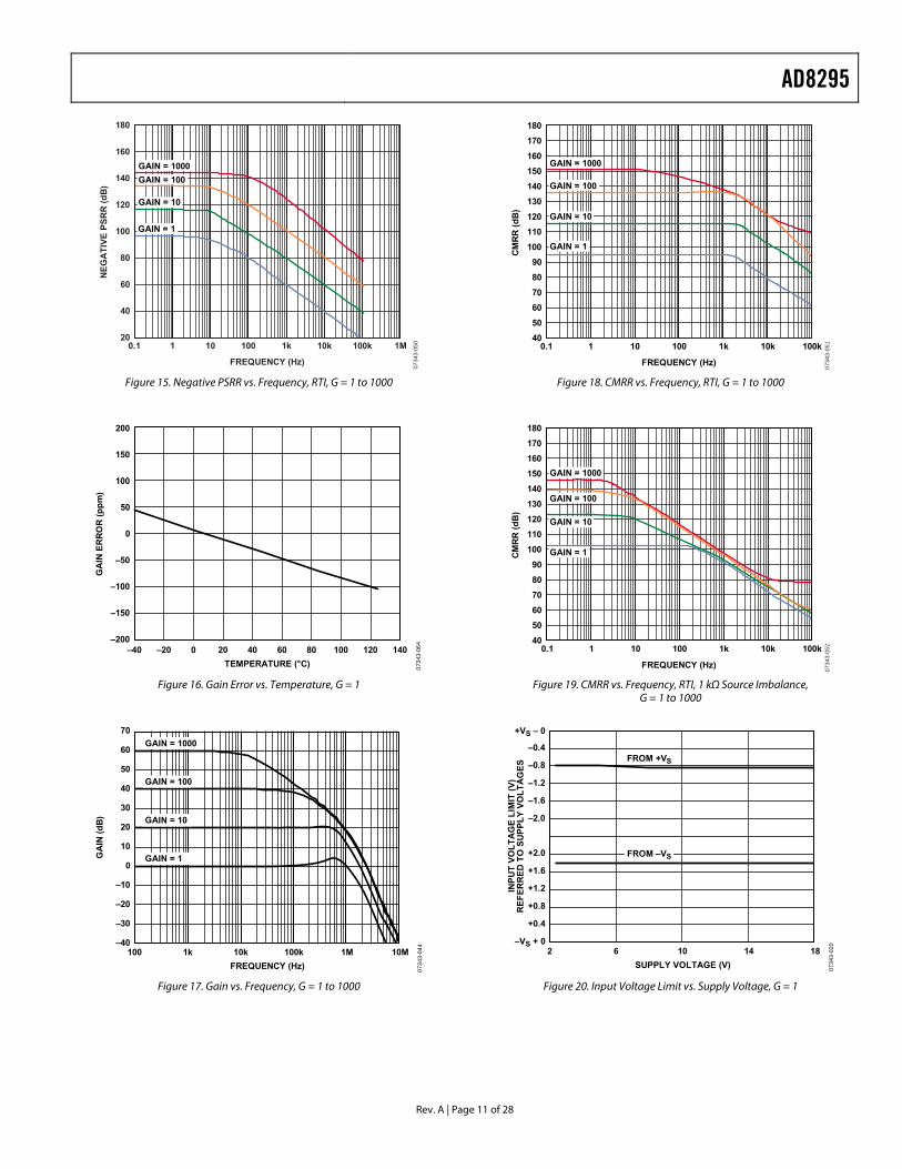
20
40
60
80
100
120
140
160
180
0.1 1 10 100 1k 10k 100k 1M
0734
3
FREQUENCY (Hz)
-050
NEG
ATI
VE P
SRR
(dB
)
405060708090
100110120130140150160170180
0.1 1 10 100 1k 10k 100k
0734
3-05
1
FREQUENCY (Hz)
CM
RR
(dB
)
GAIN = 1000
GAIN = 100
GAIN = 10
GAIN = 1
GAIN = 1000GAIN = 100
GAIN = 10
GAIN = 1
–150
–200–40 –20 0 20 40 60 80 100 120 140
Figure 15. Negative PSRR vs. Frequency, RTI, G = 1 to 1000
200
150
100
50
0
–50
–100
GA
IN E
RR
OR
(ppm
)
TEMPERATURE (°C) 0734
Figure 18. CMRR vs. Frequency, RTI, G = 1 to 1000
0.1 1 10 100 1k 10k 100k405060708090
100110120130140150160170180
3-06
4
Figure 16. Gain Error vs. Temperature, G = 1
70
–20
–10
0
10
20
30
40
50
60
GA
IN (d
B)
–40
–30
100 1k 10k 100k 1M 10MFREQUENCY (Hz)
GAIN = 1
GAIN = 10
GAIN = 100
GAIN = 1000
0734
3-04
4
Figure 17. Gain vs. Frequency, G = 1 to 1000
0734
3-05
2
FREQUENCY (Hz)
CM
RR
(dB
)
GAIN = 1000
GAIN = 100
GAIN = 10
GAIN = 1
Figure 19. CMRR vs. Frequency, RTI, 1 kΩ Source Imbalance, G = 1 to 1000
–VS + 0
+0.4
+0.8
+1.2
+1.6
+2.0
FROM +VS
INPU
T VO
LTA
GE
LIM
IT (V
)R
EFER
RED
TO
SU
PPLY
VO
LTA
GES
–2.0
–1.6
–1.2
–0.8
–0.4
+V – 0S
FROM –VS
2 6 10 14 18SUPPLY VOLTAGE (V) 07
343-
020
Figure 20. Input Voltage Limit vs. Supply Voltage, G = 1
AD8295
Rev. A | Page 12 of 28
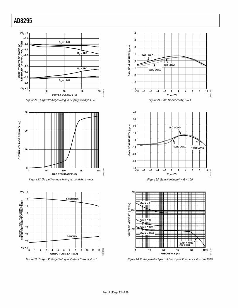
OU
TPU
T VO
LTA
GE
SWIN
G (V
)R
EFER
RED
TO
SU
PPLY
VO
LTA
GES
RL = 2kΩ
RL = 10kΩ
–1.6
–1.2
–0.4
+VS – 0
–0.8
RL = 10kΩ
RL = 2kΩ
+0.4
–VS + 0
+0.8
+1.2
+1.6
2 6 10 14 18SUPPLY VOLTAGE (V) 07
343-
021
Figure 21. Output Voltage Swing vs. Supply Voltage, G = 1
30
0
10
20
1 10 100 1k 10k
OU
TPU
T VO
LTA
GE
SWIN
G (V
p-p
)
LOAD RESISTANCE (Ω) 0734
3-02
2
Figure 22. Output Voltage Swing vs. Load Resistance
OU
TPU
T VO
LTA
GE
SWIN
G (V
)R
EFER
RED
TO
SU
PPLY
VO
LTA
GES
+VS – 0
–1
–2
–3
+3
+2
+1
–VS + 00 121110987654321
OUTPUT CURRENT (mA)
SINKING
SOURCING
0734
3-02
3
Figure 23. Output Voltage Swing vs. Output Current, G = 1
–10 –8 –6 –4 –2 0 2 4 6 8 10VOUT (V)
GA
IN N
ON
LIN
EAR
ITY
(ppm
)
2kΩ LOAD
600Ω LOAD
10kΩ LOAD
4
3
2
1
0
–1
–2
–3
–4
0734
3-02
4
Figure 24. Gain Nonlinearity, G = 1
–10 –8 –6 –4 –2 0 2 4 6 8 10VOUT (V)
GA
IN N
ON
LIN
EAR
ITY
(ppm
)2kΩ LOAD
600Ω LOAD 10kΩ LOAD
40
30
20
10
0
–10
–20
–30
–40
0734
3-02
5
Figure 25. Gain Nonlinearity, G = 100
1 101
10
100
1k
100 1k 10k 100kFREQUENCY (Hz)
VOLT
AG
E N
OIS
E R
TI (n
V/√H
z) GAIN = 1
GAIN = 10
GAIN = 100
GAIN = 1000
GAIN = 1000BW LIMIT
0734
3-02
7
Figure 26. Voltage Noise Spectral Density vs. Frequency, G = 1 to 1000

AD8295
Rev. A | Page 13 of 28
2µV/DIV 1s/DIV 0734
3-02
8
0.1µV/DIV 1s/DIV
Figure 27. 0.1 Hz to 10 Hz RTI Voltage Noise, G = 1
0734
3-02
9
1 10 100 1k 10k 100kFREQUENCY (Hz)
10
Figure 28. 0.1 Hz to 10 Hz RTI Voltage Noise, G = 1000
1k
100
CU
RR
ENT
NO
ISE
(fA/
Hz)
0734
3-03
0
5pA/DIV 1s/DIV
Figure 29. Current Noise Spectral Density vs. Frequency
0734
3-03
1
1k 10k 100k 1MFREQUENCY (Hz)
Figure 30. 0.1 Hz to 10 Hz Current Noise
30
25
20
15
10
5
0
MA
X O
UTP
UT
VOLT
AG
E (V
p-p
)
GAIN = 1
GAIN = 10, 100, 1000
0734
3-03
2
Figure 31. Large Signal Frequency Response
5V/DIV
0.002%/DIV
7.4µs TO 0.01%8.3µs TO 0.001%
20µs/DIV
0734
3-03
3
Figure 32. Large Signal Pulse Response and Settling Time, G = 1

AD8295
Rev. A | Page 14 of 28
5V/DIV
4.8µs TO 0.01%6.6µs TO 0.001%
0.002%/DIV
20µs/DIV
0734
3-03
4
Figure 33. Large Signal Pulse Response and Settling Time, G = 10
5V/DIV
20µs/DIV
0.002%/DIV
9.2µs TO 0.01%16.2µs TO 0.001%
0734
3-03
5
Figure 34. Large Signal Pulse Response and Settling Time, G = 100
5V/DIV
0.002%/DIV
83µs TO 0.01%112µs TO 0.001%
200µs/DIV
0734
3-03
6
Figure 35. Large Signal Pulse Response and Settling Time, G = 1000
4µs/DIV20mV/DIV
0734
3-03
7
Figure 36. Small Signal Pulse Response, G = 1, RL = 2 kΩ, CL = 100 pF
4µs/DIV20mV/DIV
0734
3-03
8
Figure 37. Small Signal Pulse Response, G = 10, RL = 2 kΩ, CL = 100 pF
10µs/DIV20mV/DIV
0734
3-03
9
Figure 38. Small Signal Pulse Response, G = 100, RL = 2 kΩ, CL = 100 pF
AD8295
Rev. A | Page 15 of 28
100µs/DIV20mV/DIV
1 10 100
SETTLED TO 0.01%
SETTLED TO 0.001%
1kGAIN
1k
10
100
1
SETT
LIN
G T
IME
(µs)
0734
3-04
0
00 5 10 15 20
OUTPUT VOLTAGE STEP SIZE (V)
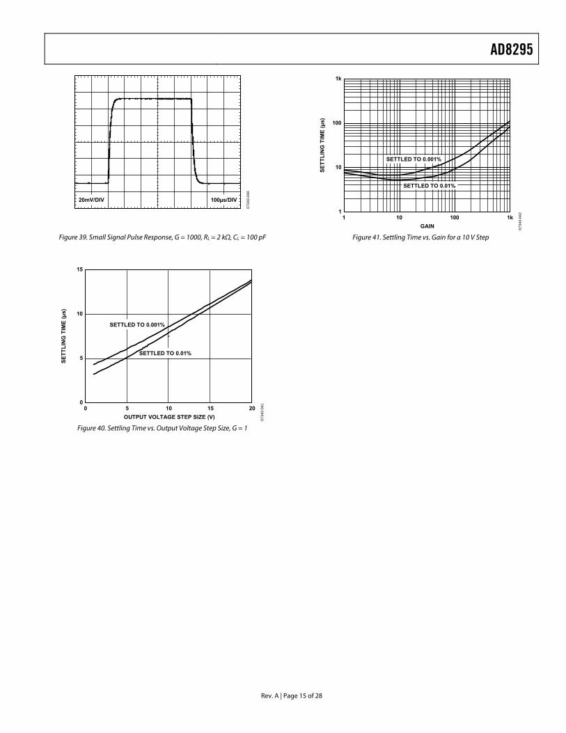
Figure 39. Small Signal Pulse Response, G = 1000, RL = 2 kΩ, CL = 100 pF
15
10
5SETT
LIN
G T
IME
(µs)
SETTLED TO 0.01%
SETTLED TO 0.001%
0734
3-04
2
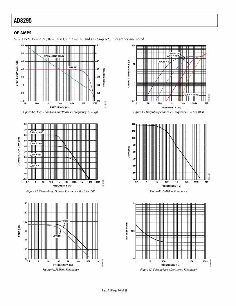
Figure 41. Settling Time vs. Gain for a 10 V Step
0734
3-04
1
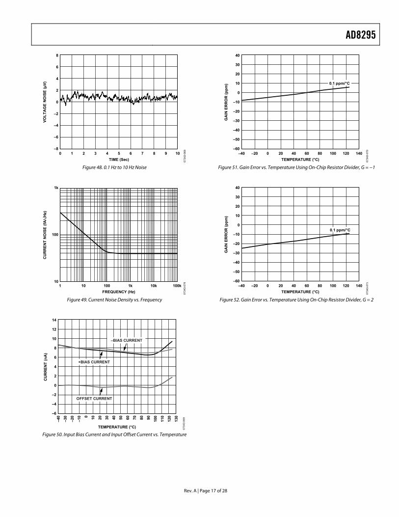
Figure 40. Settling Time vs. Output Voltage Step Size, G = 1
AD8295
Rev. A | Page 16 of 28
OP AMPS VS = ±15 V, TA = 25°C, RL = 10 kΩ, Op Amp A1 and Op Amp A2, unless otherwise noted.
–4010 100 1k 10k 100k 1M 10M
–270
0734
3-07
3FREQUENCY (Hz)
–20
0
20
40
60
80
100
–225
–180
–135
–90
–45
0
45
PHA
SE (D
egre
es)
OPE
N-L
OO
P G
AIN
(dB
)
OPEN-LOOP GAIN
PHASE
Figure 42. Open-Loop Gain and Phase vs. Frequency, CL = 5 pF
80
70
60
50
40
30
20
10
0
–10
CLO
SED
-LO
OP
GA
IN (d
B)
–200.1 1 10 100 1k 10k 100k 1M 10M 100M
FREQUENCY (Hz) 0734
3-06
5
GAIN = 1
GAIN = 10
GAIN = 100
GAIN = 1000
Figure 43. Closed-Loop Gain vs. Frequency, G = 1 to 1000
140
120
100
80
60
40
PSR
R (d
B)
200.1 1 10 100 1k 10k 100k 1M
FREQUENCY (Hz) 0734
3-06
6
+PSRR
–PSRR
Figure 44. PSRR vs. Frequency
0734
3-07
4
FREQUENCY (Hz)
OU
TPU
T IM
PED
AN
CE
(Ω)
10.1
1
10
100
10 100 1k 10k 100k 1M
GAIN = 10GAIN = 100
GAIN = 1
GAIN = 1000
Figure 45. Output Impedance vs. Frequency, G = 1 to 1000
40
50
60
70
80
90
100
110
120
0.1 1 10 100 1k 10k 100k 1M
0734
3-07
5
FREQUENCY (Hz)
CM
RR
(dB
)
Figure 46. CMRR vs. Frequency
1k
100
101 10 100 1k 10k 100k
NO
ISE
(nV/
Hz)
FREQUENCY (Hz) 0734
3-06
7
Figure 47. Voltage Noise Density vs. Frequency
AD8295
Rev. A | Page 17 of
8
6
4
2
0
–2
–4
–6
–80 1 2 3 4 5 6 7 8 9 10
VOLT
AG
E N
OIS
E (µ
V)
28
TIME (Sec) 0734
3-1k
100
CU
RR
ENT
NO
ISE
(fA/
Hz)
068
1 10 100 1k 10k 100k 07810
Figure 48. 0.1 Hz to 10 Hz Noise
FREQUENCY (Hz) 0734
3-
Figure 49. Current Noise Density vs. Frequency
14
12
10
8
6
4
2
0
–2
CU
RR
ENT
(nA
)
–4
–6
–40
–30
–20
–10 0 10 20 30 40 50 60 70 80 90 100
110
120
130
TEMPERATURE (°C)
OFFSET CURRENT
+BIAS CURRENT
–BIAS CURRENT
0734
3-06
9
40
30
20
10
0
–10
–20
–30
–40
–50
–60–40 –20 0 20 40 60 80 100 120 140
GA
IN E
RR
OR
(ppm
)
TEMPERATURE (°C)
Figure 50. Input Bias Current and Input Offset Current vs. Temperature
0.1 ppm/°C
40
30
20
10
0
–10
–20
–30
–40
–50
–60–40 –20 0 20 40 60 80 100 120 140
GA
IN E
RR
OR
(ppm
)
TEMPERATURE (°C)
0734
3-07
0
Figure 51. Gain Error vs. Temperature Using On-Chip Resistor Divider, G = −1
0.1 ppm/°C
0734
3-07
1
Figure 52. Gain Error vs. Temperature Using On-Chip Resistor Divider, G = 2
AD8295
Rev. A | Page 18 of 28
SYSTEM VS = ±15 V, VREF = 0 V, TA = 25°C, unless otherwise noted.
50 07
FREQUENCY (Hz)
10 100 1k 10k 100k 1M
70
90
110
130
150
170
343-
076
CH
AN
NEL
SEP
AR
ATI
ON
, RTI
(dB
)
GAIN = 1
GAIN = 1000
Figure 53. Channel Separation vs. Frequency (Source Channel: Op Amp with RL = 2 kΩ; Receive Channel: In-Amp at G = 1 and G = 1000)
0
10
20
30
40
50
60
70
1 10 100 1k 10k 100k 1M
80
0734
3-05
5
FREQUENCY (Hz)
CO
MM
ON
-MO
DE
OU
TPU
T (d
B)
Figure 56. Differential Output Configuration, Common-Mode Output vs. Frequency
110 07
FREQUENCY (Hz)
10 100 1k 10k 100k 1M
120
130
140
150
160
343-
077
CH
AN
NEL
SEP
AR
ATI
ON
, RTI
(dB
)
Figure 54. Channel Separation vs. Frequency (Source Channel: In-Amp with RL = 2 kΩ, G = 1; Receive Channel: Op Amp at G = 1000)
3.0
2.5
2.0
1.5
1.0
0.5
02 4 6 8 10 12 14 16
SUPP
LY C
UR
REN
T (m
A)
SUPPLY VOLTAGE (±VS)
+125°C
+85°C+25°C
–40°C
0734
3-07
2
Figure 57. Supply Current vs. Supply Voltage
–4010 100 1k 10k 100k 1M 10M
0734
3-05
4
FREQUENCY (Hz)
–20
0
20
40
60
80
GA
IN (d
B)
GAIN = 1000
GAIN = 100
GAIN = 10
GAIN = 1
Figure 55. Differential Output Configuration, Gain vs. Frequency, G = 1 to 1000

AD8295
Rev. A | Page 19 of 28
THEORY OF OPERATION As shown in Figure 58, the AD8295 contains a precision instrumentation amplifier, two uncommitted op amps, and a precision resistor array. These components allow many common applications to be wired using simple pin-strapping, directly at the IC. This not only saves printed circuit board (PCB) space but also improves circuit performance because both temperature drift and resistor tolerance errors are reduced.
A1 OUT A1 R2
A2 +IN A2 –IN
–IN
RG
+VS OUT
RG
+IN
–VS REF
1
2
3
4
8765
13141516
A1
IA
A2
R120kΩ
R220kΩ
A2 OUTAD8295
A1 +IN
A1 R1
A1 –IN
12
11
10
9
407
343-
00
Figure 58. Functional Block Diagram
UNCOMMITTED OP AMPS The AD8295 has two uncommitted op amps that can be used independently. These op amps allow simple pin-strapping for many common applications circuits.
Op Amp A1 has its inverting input connected to a precision 2:1 voltage divider resistor network. Because this network is internal to the IC, these resistors are closely matched and also track each other, with temperature variations. Op Amp A1 and the associated resistor network can be used to create either a noninverting gain stage of 2 or an inverting gain stage of −1 with excellent gain accuracy and gain drift.
Op Amp A2 is a more conventional op amp, with standard inverting and noninverting inputs and an output.
INSTRUMENTATION AMPLIFIER Gain Selection
The transfer function of the AD8295 is
VOUT = G × (VIN+ − VIN−) + VREF
where placing a resistor across the RG terminals sets the gain of the AD8295 according to the following equation:
GRG 1+=
kΩ4.49
Resistor values can be obtained by referring to Table 9 or by using the following gain equation:
1kΩ4.49−
=G
RG
Table 9. Gains Achieved Using 1% Resistors 1% Standard Table Value of RG Calculated Gain 49.9 kΩ 1.990 12.4 kΩ 4.984 5.49 kΩ 9.998 2.61 kΩ 19.93 1.00 kΩ 50.40 499 Ω 100 249 Ω 199.4 100 Ω 495 49.9 Ω 991
The AD8295 defaults to G = 1 when no gain resistor is used. Gain accuracy is a combination of both the RG accuracy and the accuracy listed in the specifications in Table 2, including accuracy over temperature. Gain error and gain drift are kept to a minimum when the gain resistor is not used.
Common-Mode Input Voltage Range
The AD8295 in-amp architecture applies gain internally and then removes the common-mode voltage. Therefore, internal nodes in the AD8295 experience a combination of both the gained signal and the common-mode signal. This combined signal can be limited by the voltage supplies even when the individual input and output signals are not. Figure 7 through Figure 10 show the allowable common-mode input voltage ranges for various output voltages and supply voltages.
If Figure 7 through Figure 10 indicate that internal voltage limiting may be an issue, the common-mode range can be significantly improved by lowering the gain in the instrumen-tation amplifier by one half and applying a second G = 2 stage. Figure 59 shows how to do this amplification with the internal circuitry of the AD8295, requiring no additional external components.
REFA1
+IN
–IN
R220kΩ
A1 OUT
TOTAL GAIN = IN-AMP GAIN × 2
+
–
IN-AMP+
–RG
R120kΩ
0734
3-01
9
Figure 59. Applying Gain in a Later Stage Allows Wider Input
Common-Mode Range
AD8295
Rev. A | Page 20 of 28
Reference Terminal
The output voltage of the AD8295 instrumentation amplifier is developed with respect to the potential on the reference terminal (REF). This is useful when the output signal needs to be offset to a precise dc level.
The reference pin input can be driven slightly beyond the rails. The REF pin is protected with ESD diodes, and the REF voltage should not exceed either +VS or −VS by more than 0.3 V.
For best performance, the source impedance to the REF terminal should be kept below 1 Ω. Additional impedance at the REF terminal can significantly degrade the CMRR of the amplifier. When the reference source has significant output impedance (for example, a resistive voltage divider), buffer the signal before driving the REF pin. Internal Op Amp A1 or A2 can be used for this purpose, as shown in Figure 60.
0734
3-01
0
+VS REF
AD8295
REFRA
+VS
RBRA
RB
C OP AMPBUFFER
AD8295
INCORRECT CORRECT
+
Figure 60. Driving the Reference Pin
Noise at the reference feeds directly to the output. Therefore, in Figure 60, Capacitor C is added to filter out any high frequency noise on the positive power supply line. For very clean supplies, the capacitor may not be needed. The filter frequency is a trade-off between noise rejection and start-up time, and is given by the following equation:
BA
BAPASSLOW
RRRR
Cf
+π
=−
2
1
LAYOUT The AD8295 is a high precision device. To ensure optimum performance at the PCB level, care must be taken in the board layout. The AD8295 pins are arranged in a logical manner to aid in this task.
Routing and Vias
Unlike most LFCSP packages, the AD8295 package was designed without the thermal pad to allow routes and vias directly beneath the chip. However, the manufacturing process leaves a very small section of exposed metal at each of the package corners. This metal is connected to –VS through the part. Because of the possibility of a short, vias should not be placed under this exposed metal.
Careful board layout maximizes system performance. Traces from the gain setting resistor to the RG pins should be kept as short as possible to minimize parasitic inductance. To ensure the most accurate output, the trace from the REF pin should either be connected to the local ground of the AD8295 or to a voltage that is referenced to the local ground of the AD8295.
Common-Mode Rejection over Frequency
The AD8295 has a higher CMRR over frequency than typical in-amps, which gives it greater immunity to disturbances such as line noise and its associated harmonics. The AD8295 pinout and hidden paddle package were designed so that the board designer can take full advantage of this performance with a well-implemented layout.
Poor layout can cause some of the common-mode signal to be converted to a differential signal before it reaches the in-amp. Such conversions occur when one input path has a frequency response that is different from the other. To keep CMRR across frequency high, the input source impedance and capacitance of each path should be closely matched. Additional source resistance in the input path (for example, for input protection) should be placed close to the in-amp inputs to minimize their interaction with parasitic capacitance from the PCB traces.
Parasitic capacitance at the gain setting pins can also affect CMRR over frequency. The traces to the RG resistor should be kept as short as possible. If the board design has a component at the gain setting pins (for example, a switch or jumper), the part should be chosen so that the parasitic capacitance is as small as possible.
Unused Op Amps
When not in use, the internal op amps should be connected in a unity-gain configuration, with the noninverting input connected to a bias point in the input range of the op amp. These connections ensure that the AD8295 op amp uses minimum power and does not disturb the internal power supplies of the AD8295. These connections are shown as dotted lines in several of the applica-tions figures.
Reference
The output voltage of the instrumentation amplifier section of the AD8295 is developed with respect to the potential on the reference terminal (REF); care should be taken to tie the REF pin to the appropriate local ground (see Figure 61).
AD8295
Rev. A | Page 21 of 28
Power Supplies
A stable dc voltage should be used to power the instrumentation amplifier. Noise on the supply pins can adversely affect perfor-mance. See the PSRR performance curves in Figure 14 and Figure 15 for more information.
A 0.1 μF capacitor should be placed as close as possible to each supply pin. An additional capacitor, a 10 μF tantalum for the lower frequencies, can be used farther away from the IC. In most cases, the 10 μF bypass capacitor can be shared by other integrated circuits on the same PCB.
AD8295IN-AMP
+VS
+IN
RG
–INLOAD
REF
0.1µF 10µF
0.1µF 10µF
–VS
VOUT
0734
3-00
5
Figure 61. Supply Decoupling, REF, and Output Referred to Local Ground
INPUT PROTECTION All terminals of the AD8295 are protected against ESD by diodes at the inputs. If voltages beyond the supplies are anti-cipated, resistors should be placed in series with the inputs to limit the current. Resistors should be chosen so that current does not exceed 6 mA into the internal ESD diodes in the over-load condition. These resistors can be the same as those used for RFI protection. (See the RF Interference section for more information.)
For applications where the AD8295 encounters extreme overload voltages, as in cardiac defibrillators, external series resistors and low leakage diode clamps, such as BAV199Ls, FJH1100s, or SP720s can be used.
INPUT BIAS CURRENT RETURN PATH The input bias currents of the AD8295 must have a return path to common. When the source, such as a thermocouple, cannot provide a return current path, one should be created, as shown in Figure 62. Otherwise, the input currents charge up the input capacitance until the in-amp is turned off or saturated.
THERMOCOUPLE
+VS
REF
–VS
CAPACITIVELY COUPLED
+VS
REF
C
C
–VS
AD8295IN-AMP
AD8295IN-AMP
TRANSFORMER
+VS
REF
–VS
INCORRECT
CAPACITIVELY COUPLED
+VS
REF
–VS
TRANSFORMER
+VS
REF
–VS
10MΩ
CORRECT
AD8295IN-AMP
AD8295IN-AMP
AD8295IN-AMP
THERMOCOUPLE
+VS
REF
C
R
R
C
–VS
1fHIGH-PASS = 2πRC AD8295IN-AMP
0734
3-00
6
Figure 62. Creating an Input Bias Current Return Path
RF INTERFERENCE RF interference is often a problem when amplifiers are used in applications where there are strong RF signals. The precision circuits in the AD8295 can rectify the RF signals so that they appear as a dc offset voltage error. To avoid this rectification, place a low-pass filter before the input. Figure 63 shows such a network in front of the instrumentation amplifier. The filter limits both the differential and common-mode bandwidth, as shown in the following equations:
)2(π2 CD CCR +1)(FILTER Difff =
CFILTER RC
CMfπ2
1)( =
where CD ≥ 10CC.

AD8295
Rev. A | Page 22 of 28
R
R
AD8295IN-AMP
+VS
+IN
–IN
0.1µF 10µF
10µF0.1µF
REF
VOUT
–VS
CD
CC
CC
10nF
1nF
1nF
0734
3-00
7
4.02kΩ
4.02kΩ
RG
Figure 63. RFI Suppression
Lower cutoff frequencies improve RFI robustness. Accuracy of the CC capacitors is important, because any mismatch between the R × CC at the positive input and the R × CC at the negative input degrades the CMRR of the AD8295. Keeping CD at least 10 times larger than CC is recommended.
DIFFERENTIAL OUTPUT The AD8295 can be pin-strapped to provide a differential output; the simplified schematic is shown in Figure 64 and the full pin connection is shown in Figure 65. This configuration uses the instrumentation amplifier to maintain the differential voltage, while the op amp maintains the common-mode voltage. Because the in-amp precisely controls the output relative to its reference pin, this circuit has the same excellent dc performance as the single-ended output configuration. The transfer function for the differential and common-mode outputs are as follows:
VDIFF_OUT = VOUT+ − VOUT− = G × (VIN+ − VIN−)
VCM_OUT = (VOUT+ + VOUT−)/2 = VREF
where:
GRG
kΩ4.491+=
This configuration is fully specified (see Table 2, Figure 55, and Figure 56). DC performance is the same as for the single-ended configuration; ac performance is slightly different.
+IN
–IN
REF
IN-AMP
VREF INPUT20kΩ
+–A1
+OUT
–OUT
0734
3-01
8
20kΩ
+
–
Figure 64. Differential Output Configuration Using an Op Amp
A1OUT
A1R2
A2+IN
A2–IN
–IN–INPUT
+INPUT
RG
+VS
+VS
0.1µF–VS
–VS
OUT
REF
RG
+IN
1
2
3
4
8765
13141516
A1
IA
A2
R120kΩ
R220kΩ
A2OUTAD8295
A1+IN VREF
INPUT
+OUT
–OUT
A1R1
A1–IN
12
11
10
9
0.1µF
NOTES1. CONNECT AS SHOWN IF A2 IS NOT BEING USED. 07
343-
008
Figure 65. Minimum Component Connections for Differential Output
An alternative differential output configuration, which also requires no external components, is shown in Figure 66. Unlike the circuits shown in Figure 64 and Figure 65, this configuration uses an inverting op amp configuration to double the gain from the instrumentation amplifier. Because this configuration requires less gain from the instrumentation amplifier, it can have a wider frequency response and a wider input common-mode range vs. output voltage. However, because it does not take advantage of feedback at the reference pin of the instrumentation amplifier, dc performance includes the errors from the op amp and the resistor network. When using the internal precision components of the AD8295, these errors have a minimal effect on overall accuracy. This configuration is not specified in this data sheet.
REF
VREF INPUT
A1
+IN
–IN
R220kΩ
+OUT
–OUT–
+
IN-AMP+
–
R120kΩ
RG
0734
3-04
3
Figure 66. Alternative Differential Output Configuration
AD8295
Rev. A | Page 23 of
APPLICATIONS INFORMATION CREATING A REFERENCE VOLTAGE AT MIDSCALE HIGH ACCURACY G = −1 CONFIGURATION WITH
LOW-PASS FILTER A reference voltage other than ground is often useful, for example, when driving a single-supply ADC. Creating a reference voltage derived from a voltage divider is straight-forward with the AD8295 (see Figure 67). In this configuration, Op Amp A2 is used to provide a buffered VS/2 reference for the in-amp section. This configuration is very similar to the one described in the Reference Terminal section.
The circuit in Figure 68 uses Op Amp A1 and the resistor string to provide a precise G = −1 configuration. Because no external resistors are used to set the gain, gain accuracy and gain drift depend only on the internally matched resistors, yielding excel-lent performance.
Adding a capacitor across Resistor R2 is a simple way to provide a single-pole low-pass filter that rolls off at 20 dB per decade. This capacitor is shown as C1 in Figure 68.
Note that the internal resistors of Op Amp A1 are not used to provide VS/2. Instead, external 1% (or better) resistors are used. Because the negative input of Op Amp A1 is permanently connected to the junction of internal resistors R1 and R2, Op Amp A1 operates as a low voltage clamp, preventing the resistor string from providing a convenient VS/2 voltage.
A1OUT
A1R2
A2+IN
A2–IN
–IN
28
Noise at the reference feeds directly to the output, so if the reference voltage is derived from a noisy source, filtering is required. In Figure 67, Capacitor C1 has been added to filter out high frequency noise on the positive power supply line. The 10 μF capacitor and the 100 kΩ resistors shown in Figure 67 roll off noise starting at 0.3 Hz. The filter frequency is a trade-off between noise rejection and start-up time.
A1 A1
A2+IN
A2–IN+VS
+
OUT R2
VS
OUT
REF
1
2
3
4
865
131416
A1
IA
A2
R120kΩ
R220kΩ
100kΩ
100kΩ
A2OUT
C110µF
AD8295
A1+IN
A1R1
A1–IN
12
11
10
9
0907
343-
0
7
–IN–INPUT
OUTPUT
+INPUT
RG
RG
+IN
15
+VS
0.1µF
VS/2BUFFERED
Figure 67. Single-Supply Connection with Buffered Reference
–INPUT
+INPUT
RG
+VS
–VS
OUT
RG
+IN
16 15 14 13
1
2
3
4
8765
A1
IA
A2
R120kΩ
R220kΩ
A2OUTAD8295
VREF INPUT
VREF INPUTLOW-PASSFILTEREDOUTPUT
VREFBUFFERED
C1
A1R1
A1–IN
12
11
10
9
NOTES1. fLOW-PASS = 1/(2π 20kΩ C1). 07
343-
011
Figure 68. Single-Pole Output Filter Using a Single External Capacitor
If the connections to Pin 10 and Pin 11 in Figure 68 are changed so that Pin 10 connects to ground and Pin 11 connects to the in-amp output, the result is a G = 2 circuit, also with excellent gain accuracy and drift. In the G = 2 configuration, Capacitor C1 lowers the gain from 2 to 1 at higher frequencies.
AD8295
Rev. A | Page 24 of 28
TWO-POLE SALLEN-KEY FILTER Figure 69 shows the in-amp output section of the AD8295 being low-pass filtered using a two-pole Sallen-Key filter. The filter section consists of Op Amp A2, External Resistors R1 and R2, as well as Capacitors C1 and C2. Resistor R3 compensates for input offset current errors and is equal to the parallel combination of R1 and R2. The ratio of capacitance between C1 and C2 sets the filter quality factor, Q. For most applications, a filter Q of 0.5 to 0.7 provides a good trade-off between performance and sta-bility. High Q, nonpolarized capacitors, such as NPO ceramic, should be used. The exact pole frequencies are dependent on the tolerance of the resistors and capacitors used.
A1OUT
A1R2
A2+IN
A2–IN
–IN–INPUT
+INPUT
RG
+VS
+VS
OUT
R1
R2
C2
RG
+IN
0.1µF–VS
–VS
REF
1
2
3
4
8765
13141516
A1
IA
A2
R120kΩ
R220kΩ
A2OUTAD8295
A1+IN
LOW-PASSFILTEREDOUTPUT
A1R1
A1–IN
12
11
10
9
0.1µFR3
C1
0734
3-01
2
Figure 69. Two-Pole Sallen-Key Filter
The design equations for a Sallen-Key filter can be greatly simplified if the resistors and capacitors are made equal. When C1 = C2 and R1 = R2, Q is 0.5 and the design equation simplifies to
f = 1/(2πRC)
where R is in ohms and C is in farads.
For example, with R1 = R2 = 10 kΩ, and C1 = C2 = 2.2 nF,
f = 7.2 kHz
When C1 is not equal to C2 and R1 is not equal to R2, the values of Q and the cutoff frequency are calculated as follows:
)( R2R1C2 +
C2C1R2R1Q =
C2 C1 R2 R1f
π=
21
AC-COUPLED INSTRUMENTATION AMPLIFIER The circuit in Figure 70 provides a single-pole high-pass filter, using only one external capacitor.
At low frequencies, Capacitor C1 has a high impedance, thus operating Op Amp A1 at high gain (G = XC/20 kΩ). Because of its high gain, Op Amp A1 is able to drive the in-amp reference pin until it forces the output of the in-amp to 0 V. Therefore, no signal appears at the circuit output.
At higher frequencies, the gain of Op Amp A1 drops and the op amp is no longer able to maintain the in-amp output at 0 V. Therefore, at frequencies above the RC filter bandwidth, the in-amp operates in a normal manner, and the signal appears at the output.
The 3 dB corner frequency is set by Internal Resistor R1 and External Capacitor C1 as follows:
f = 1/((2π × 20 kΩ) × C1)
The precision of R1 (better than 0.2%) means that the filter bandwidth depends mainly on the tolerance of Capacitor C1.
At low frequencies, Op Amp A1 drives the appropriate voltage on the reference pin to null out the original signal. Voltage supplies should be chosen so that Op Amp A1 has enough output headroom to produce the nulling voltage.
A1 OUTA1 R2
A2 +IN A2 –IN+VS
–VS
OUT
REF
1
2
3
4
865
13141516
A1
IA
A2
R120kΩ
R220kΩ
A2 OUT
OUTPUT
AD8295
A1 +IN
A1 R1
A1 –IN
12
11
10
907
343-
015
7
C1
–IN–INPUT
RG
RG
+IN+INPUT
Figure 70. AC-Coupled Connection
AD8295
Rev. A | Page 25 of 28
If the application requires a lower frequency antialiasing filter than the one shown, increasing the capacitor values produces much better distortion results than increasing the resistor values.
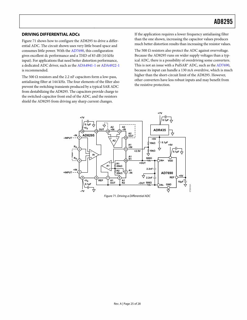
DRIVING DIFFERENTIAL ADCs Figure 71 shows how to configure the AD8295 to drive a differ-ential ADC. The circuit shown uses very little board space and consumes little power. With the AD7690, this configuration gives excellent dc performance and a THD of 83 dB (10 kHz input). For applications that need better distortion performance, a dedicated ADC driver, such as the ADA4941-1 or ADA4922-1 is recommended.
The 500 Ω resistors also protect the ADC against overvoltage. Because the AD8295 runs on wider supply voltages than a typ-ical ADC, there is a possibility of overdriving some converters. This is not an issue with a PulSAR® ADC, such as the AD7690, because its input can handle a 130 mA overdrive, which is much higher than the short-circuit limit of the AD8295. However, other converters have less robust inputs and may benefit from the resistive protection.
The 500 Ω resistors and the 2.2 nF capacitors form a low-pass, antialiasing filter at 144 kHz. The four elements of the filter also prevent the switching transients produced by a typical SAR ADC from destabilizing the AD8295. The capacitors provide charge to the switched-capacitor front end of the ADC, and the resistors shield the AD8295 from driving any sharp current changes.
+7V
A1OUT
A1R2
A2+IN
A2–IN
–IN–INPUT
+INPUT
0.1µF–VS
–7V
REF
+IN
IN– GND
REF
RG
+VS
+7V
OUT
RGVDDIN+
1
2
3
4
8765
13141516
A1
IA
A2
R120kΩ
R220kΩ
A2OUTAD8295
ADR435
A1+IN
+2.5V
+OUT
500Ω
10kΩ
10kΩ
2.2nF
A1R1
+5V+
AD7690
10µF500Ω
2.2nF
–OUT
A1–IN
12
11
10
9
0.1µF
+5V
0.1µF
0.1µF+5V
0.1µF
0734
3-01
4
Figure 71. Driving a Differential ADC
AD8295
Rev. A | Page 26 of 28
COMPLIANT TO JEDEC STANDARDS MO-263-VBBC 0623
09-B
OUTLINE DIMENSIONS
3.75BCS SQ
4.00BSC SQ
0.65BSC
0.750.600.50
TOP VIEW
12° MAX 0.80 MAX0.65 TYP
SEATINGPLANE
PIN 1INDICATOR
COPLANARITY0.08
1.000.850.80
0.350.300.25
0.05 MAX0.02 NOM
0.20 REF
BOTTOM VIEW
0.60 MAX
0.60 MAX
1.95 REFSQ
116
589
1213
4
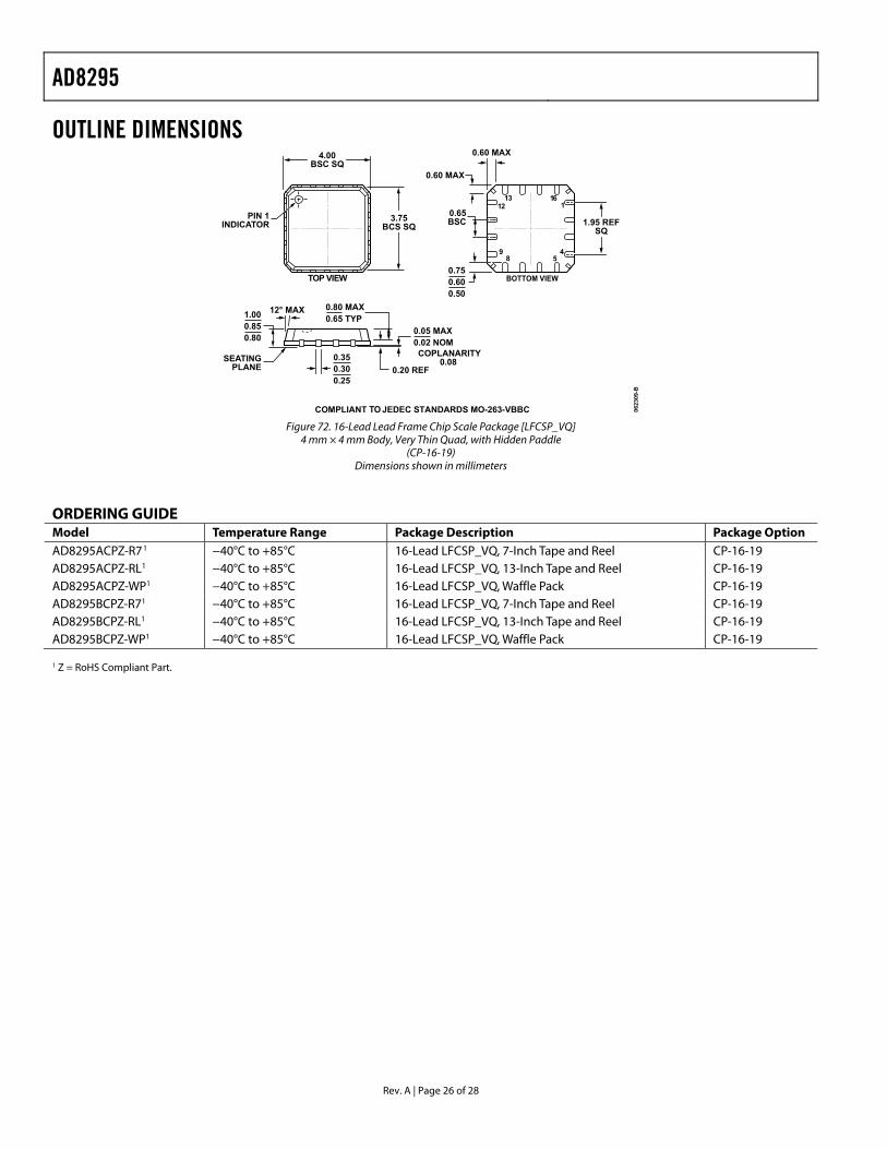
Figure 72. 16-Lead Lead Frame Chip Scale Package [LFCSP_VQ]
4 mm × 4 mm Body, Very Thin Quad, with Hidden Paddle (CP-16-19)
Dimensions shown in millimeters
ORDERING GUIDE Model Temperature Range Package Description Package Option AD8295ACPZ-R71
−40°C to +85°C 16-Lead LFCSP_VQ, 7-Inch Tape and Reel CP-16-19 AD8295ACPZ-RL1
−40°C to +85°C 16-Lead LFCSP_VQ, 13-Inch Tape and Reel CP-16-19 AD8295ACPZ-WP1
−40°C to +85°C 16-Lead LFCSP_VQ, Waffle Pack CP-16-19 AD8295BCPZ-R71
−40°C to +85°C 16-Lead LFCSP_VQ, 7-Inch Tape and Reel CP-16-19 AD8295BCPZ-RL1
−40°C to +85°C 16-Lead LFCSP_VQ, 13-Inch Tape and Reel CP-16-19 AD8295BCPZ-WP1
−40°C to +85°C 16-Lead LFCSP_VQ, Waffle Pack CP-16-19 1 Z = RoHS Compliant Part.

AD8295
Rev. A | Page 27 of 28
NOTES

AD8295
Rev. A | Page 28 of 28
NOTES
©2008–2009 Analog Devices, Inc. All rights reserved. Trademarks and registered trademarks are the property of their respective owners. D07343-0-6/09(A)