precision, rail-to-rail i/o instrumentation · pdf filetrue rail-to-rail i/o input common-mode...
TRANSCRIPT

INA326INA327
SBOS222D – NOVEMBER 2001 – REVISED NOVEMBER 2004
www.ti.com
DESCRIPTIONThe INA326 and INA327 (with shutdown) are high-perfor-mance, low-cost, precision instrumentation amplifiers withrail-to-rail input and output. They are true single-supplyinstrumentation amplifiers with very low DC errors and inputcommon-mode ranges that extends beyond the positive andnegative rails. These features make them suitable for appli-cations ranging from general-purpose to high-accuracy.
Excellent long-term stability and very low 1/f noise assurelow offset voltage and drift throughout the life of the product.
The INA326 (without shutdown) comes in the MSOP-8 pack-age. The INA327 (with shutdown) is offered in an MSOP-10.Both are specified over the industrial temperature range,–40°C to +85°C, with operation from –40°C to +125°C.
FEATURES PRECISION
LOW OFFSET: 100µV (max)LOW OFFSET DRIFT: 0.4µV/°C (max)EXCELLENT LONG-TERM STABILITYVERY-LOW 1/f NOISE
TRUE RAIL-TO-RAIL I/OINPUT COMMON-MODE RANGE:
20mV Below Negative Rail to 100mV AbovePositive Rail
WIDE OUTPUT SWING: Within 10mV of RailsSUPPLY RANGE: Single +2.7V to +5.5V
SMALL SIZEmicroPACKAGE: MSOP-8, MSOP-10
LOW COST
PRODUCTION DATA information is current as of publication date.Products conform to specifications per the terms of Texas Instrumentsstandard warranty. Production processing does not necessarily includetesting of all parameters.
Copyright © 2001-2004, Texas Instruments Incorporated
Precision, Rail-to-Rail I/OINSTRUMENTATION AMPLIFIER
Please be aware that an important notice concerning availability, standard warranty, and use in critical applications ofTexas Instruments semiconductor products and disclaimers thereto appears at the end of this data sheet.
APPLICATIONS LOW-LEVEL TRANSDUCER AMPLIFIER FOR
BRIDGES, LOAD CELLS, THERMOCOUPLES
WIDE DYNAMIC RANGE SENSORMEASUREMENTS
HIGH-RESOLUTION TEST SYSTEMS
WEIGH SCALES
MULTI-CHANNEL DATA ACQUISITIONSYSTEMS
MEDICAL INSTRUMENTATION
GENERAL-PURPOSE
INA326 AND INA327 RELATED PRODUCTSPRODUCT FEATURES
INA337 Precision, 0.4µV/°C Drift, Specified –40°C to +125°CINA114 50µV VOS, 0.5nA IB, 115dB CMR, 3mA IQ, 0.25µV/°C DriftINA118 50µV VOS, 1nA IB, 120dB CMR, 385µA IQ, 0.5µV/°C DriftINA122 250µV VOS, –10nA IB, 85µA IQ, Rail-to-Rail Output, 3µV/°C DriftINA128 50µV VOS, 2nA IB, 125dB CMR, 750µA IQ, 0.5µV/°C DriftINA321 500µV VOS, 0.5pA IB, 94dB CMRR, 60µA IQ, Rail-to-Rail Output
INA326R1
R2 C2
VIN−
VIN+
7
V+
4
V−
VO
5
6
21
83 G = 2(R2/R1)
INA327INA326

INA326, INA3272SBOS222Dwww.ti.com
SPECIFIEDPACKAGE TEMPERATURE PACKAGE ORDERING TRANSPORT
PRODUCT PACKAGE-LEAD DESIGNATOR RANGE MARKING NUMBER MEDIA, QUANTITY
INA326 MSOP-8 DGK –40°C to +85°C B26 INA326EA/250 Tape and Reel, 250" " " " " INA326EA/2K5 Tape and Reel, 2500
INA327 MSOP-10 DGS –40°C to +85°C B27 INA327EA/250 Tape and Reel, 250" " " " " INA327EA/2K5 Tape and Reel, 2500
NOTE: (1) For the most current package and ordering information, download the latest version of this data sheet and see the Package Option Addendum locatedat the end of the data sheet.
PACKAGE/ORDERING INFORMATION(1)
ABSOLUTE MAXIMUM RATINGS(1)
Supply Voltage .................................................................................. +5.5VSignal Input Terminals: Voltage(2) .............................. –0.5V to (V+) + 0.5V
Current(2) ................................................... ±10mAOutput Short-Circuit ................................................................. ContinuousOperating Temperature Range ....................................... –40°C to +125°CStorage Temperature Range .......................................... –65°C to +150°CJunction Temperature .................................................................... +150°CLead Temperature (soldering, 10s) ............................................... +300°C
NOTES: (1) Stresses above these ratings may cause permanent damage.Exposure to absolute maximum conditions for extended periods may degradedevice reliability. These are stress ratings only, and functional operation of thedevice at these or any other conditions beyond those specified is not implied.(2) Input terminals are diode clamped to the power-supply rails. Input signals thatcan swing more than 0.5V beyond the supply rails should be current limited to10mA or less.
ELECTROSTATICDISCHARGE SENSITIVITY
This integrated circuit can be damaged by ESD. TexasInstruments recommends that all integrated circuits be handledwith appropriate precautions. Failure to observe proper han-dling and installation procedures can cause damage.
ESD damage can range from subtle performance degrada-tion to complete device failure. Precision integrated circuitsmay be more susceptible to damage because very smallparametric changes could cause the device not to meet itspublished specifications.
1
2
3
4
8
7
6
5
R1
V+
VO
R2
R1
VIN−
VIN+
V−
INA326
MSOP- 8
1
2
3
4
5
10
9
8
7
6
R1
V+
VO
R2
Enable
R1
VIN−
VIN+
V−
(Connect to V+)
INA327
MSOP- 10
Top View
PIN CONFIGURATION

INA326, INA327 3SBOS222D www.ti.com
ELECTRICAL CHARACTERISTICS: VS = +2.7V to +5.5VBOLDFACE limits apply over the specified temperature range, TA = –40°C to +85°CAt TA = +25°C, RL = 10kΩ, G = 100 (R1 = 2kΩ, R2 = 100kΩ), external gain set resistors, and IACOMMON = VS /2, with external equivalent filter corner of 1kHz, unlessotherwise noted.
INA326EA, INA327EA
PARAMETER CONDITION MIN TYP MAX UNITS
INPUTOffset Voltage, RTI VOS VS = +5V, VCM = VS /2 ±20 ±100 µV
Over Temperature ±124 µVvs Temperature dVOS/dT ±0.1 ±0.4 µV/°Cvs Power Supply PSR VS = +2.7V to +5.5V, VCM = VS /2 ±20 ±3 µV/VLong-Term Stability See Note (1)
Input Impedance, Differential 1010 || 2 Ω || pFCommon-Mode 1010 || 14 Ω || pF
Input Voltage Range (V–) – 0.02 (V+) + 0.1 VSafe Input Voltage (V–) – 0.5 (V+) + 0.5 VCommon-Mode Rejection CMR VS = +5V, VCM = (V–) – 0.02V to (V+) + 0.1V 100 114 dB
Over Temperature 94 dB
INPUT BIAS CURRENT VCM = VS /2Bias Current IB VS = +5V ±0.2 ±2 nA
vs Temperature See Typical CharacteristicsOffset Current IOS VS = +5V ±0.2 ±2 nA
NOISEVoltage Noise, RTI RS = 0Ω, G = 100, R1 = 2kΩ, R2 = 100kΩ
f = 10Hz 33 nV/√Hzf = 100Hz 33 nV/√Hzf = 1kHz 33 nV/√Hzf = 0.01Hz to 10Hz 0.8 µVp-p
Voltage Noise, RTI RS = 0Ω, G = 10, R1 = 20kΩ, R2 = 100kΩf = 10Hz 120 nV/√Hzf = 100Hz 97 nV/√Hzf = 1kHz 97 nV/√Hzf = 0.01Hz to 10Hz 4 µVp-p
Current Noise, RTIf = 1kHz 0.15 pA/√Hzf = 0.01Hz to 10Hz 4.2 pAp-p
Output Ripple, VO Filtered(2) See Applications Information
GAINGain Equation G = 2(R2/R1)Range of Gain < 0.1 > 10000 V/VGain Error(3) G = 10, 100, VS = +5V, VO = 0.075V to 4.925V ±0.08 ±0.2 %
vs Temperature G = 10, 100, VS = +5V, VO = 0.075V to 4.925V ±6 ±25 ppm/°CNonlinearity G = 10, 100, VS = +5V, VO = 0.075V to 4.925V ±0.004 ±0.01 % of FS
OUTPUTVoltage Output Swing from Rail RL = 100kΩ 5 mV
RL = 10kΩ, VS = +5V 75 10 mVOver Temperature 75 mV
Capacitive Load Drive 500 pFShort-Circuit Current ISC ±25 mA
INTERNAL OSCILLATORFrequency of Auto-Correction 90 kHz
Accuracy ±20 %
FREQUENCY RESPONSEBandwidth(4), –3dB BW G = 1 to 1k 1 kHzSlew Rate(4) SR VS = +5V, All Gains, CL = 100pF Filter LimitedSettling Time(4), 0.1% tS 1kHz Filter, G = 1 to 1k, VO = 2V step, CL = 100pF 0.95 ms
0.01% 1.3 ms0.1% 10kHz Filter, G = 1 to 1k, VO = 2V step, CL = 100pF 130 µs0.01% 160 µs
Overload Recovery(4) 1kHz Filter, 50% Output Overload, G = 1 to 1k 30 µs10kHz Filter, 50% Output Overload, G = 1 to 1k 5 µs

INA326, INA3274SBOS222Dwww.ti.com
PARAMETER CONDITION MIN TYP MAX UNITS
POWER SUPPLYSpecified Voltage Range +2.7 +5.5 VQuiescent Current IQ IO = 0, Diff VIN = 0V, VS = +5V 2.4 3.4 mA
Over Temperature 3.7 mA
SHUTDOWNDisable (Logic Low Threshold) 0.25 VEnable (Logic High Threshold) 1.6 VEnable Time(5) 75 µsDisable Time 100 µsShutdown Current and Enable Pin Current VS = +5V, Disabled 2 5 µA
TEMPERATURE RANGESpecified Range –40 +85 °COperating Range –40 +125 °CStorage Range –65 +150 °CThermal Resistance θJA MSOP-8, MSOP-10 Surface-Mount 150 °C/W
NOTES: (1) 1000-hour life test at 150°C demonstrated randomly distributed variation in the range of measurement limits—approximately 10µV. (2) See ApplicationsInformation section, and Figures 1 and 3. (3) Does not include error and TCR of external gain-setting resistors. (4) Dynamic response is limited by filtering. Higherbandwidths can be achieved by adjusting the filter. (5) See Typical Characteristics, “Input Offset Voltage vs Warm-Up Time”.
ELECTRICAL CHARACTERISTICS: VS = +2.7V to +5.5V (Cont.)BOLDFACE limits apply over the specified temperature range, TA = –40°C to +85°CAt TA = +25°C, RL = 10kΩ, G = 100 (R1 = 2kΩ, R2 = 100kΩ), external gain set resistors, and IACOMMON = VS /2, with external equivalent filter corner of 1kHz, unlessotherwise noted.
INA326EA, INA327EA

INA326, INA327 5SBOS222D www.ti.com
TYPICAL CHARACTERISTICSAt TA = 25°C, VS = +5V, Gain = 100, and RL = 10kΩ with external equivalent filter corner of 1kHz, unless otherwise noted.
GAIN vs FREQUENCY1kHz FILTER
Frequency (Hz)
10 100 1k 10k 100k 1M
Gai
n (d
B)
80
60
40
20
0
−20
−40
G = 1k
G = 100
G = 10
G = 1
GAIN vs FREQUENCY10kHz FILTER
Frequency (Hz)
10 100 1k 10k 100k 1M
Gai
n (d
B)
80
60
40
20
0
−20
−40
G = 1k
G = 100
G = 10
G = 1
COMMON- MODE REJECTION vs FREQUENCY1kHz FILTER
Frequency (Hz)
10 100 1k 10k 100k 1M
CM
R (
dB)
160
140
120
100
80
60
40
20
G = 1k
G = 100
G = 10
G = 1
COMMON- MODE REJECTION vs FREQUENCY10kHz FILTER
Frequency (Hz)
10 100 1k 10k 100k 1M
CM
R (
dB)
160
140
120
100
80
60
40
20
G = 100
G = 10G = 1
G = 1k
POWER- SUPPLY REJECTION vs FREQUENCY
Frequency (Hz)
10 100 1k 10k 100k
PS
R (
dB)
120
100
80
60
40
20
0
G = 100, 1k
G = 10
G = 1
Filter Frequency10kHz1kHz
INPUT- REFERRED VOLTAGE NOISE AND INPUT BIAS CURRENT NOISE vs FREQUENCY
10kHz FILTER
1
10k
1k
100
10
1
0.1
0.01
0.00110 100 1k 10k
Frequency (Hz)
Inpu
t-R
efer
red
Vol
tage
Noi
se (
nV/√
Hz)
Inpu
t Bia
s C
urre
nt N
oise
(pA
/√H
z)G = 1
G = 100
Current Noise(all gains)
G = 10
G = 1000

INA326, INA3276SBOS222Dwww.ti.com
TYPICAL CHARACTERISTICS (Cont.)At TA = 25°C, VS = +5V, Gain = 100, and RL = 10kΩ with external equivalent filter corner of 1kHz, unless otherwise noted.
SMALL- SIGNAL RESPONSEG = 1, 10, AND 100
50m
V/d
iv
500µs/div
1kHz Filter
10kHz Filter
SMALL- SIGNAL STEP RESPONSEG = 1000
50m
V/d
iv
500µs/div
1kHz Filter
LARGE- SIGNAL RESPONSEG = 1 TO 1000
2V/d
iv
500µs/div
1kHz Filter
10kHz Filter
INPUT OFFSET VOLTAGE vs TURN- ON TIME1kHz FILTER, G = 100
Inpu
t Offs
et V
olta
ge (
20µV
/div
)
10 2
Turn- On Time (ms)
FilterSettling
Time
DeviceTurn- On
Time(75µs)
INPUT OFFSET VOLTAGE vs WARM- UP TIME10kHz FILTER, G = 100
Inpu
t Offs
et V
olta
ge (
20µV
/div
)
0.2 0.30 0.1 0.4
Warm- Up Time (ms)
FilterSettling
Time
DeviceTurn- On
Time
0.01Hz TO 10Hz VOLTAGE NOISE
200n
V/d
iv
10s/div

INA326, INA327 7SBOS222D www.ti.com
TYPICAL CHARACTERISTICS (Cont.)At TA = 25°C, VS = +5V, Gain = 100, and RL = 10kΩ with external equivalent filter corner of 1kHz, unless otherwise noted.
OFFSET VOLTAGE DRIFT PRODUCTION DISTRIBUTIONG = 1
Offset Voltage Drift (µV/°C)
0 2 4 6 8 10 12 14 16 18 20 22 24 26 28 30 32 34 36 38 40
Pop
ulat
ion
OFFSET VOLTAGE PRODUCTION DISTRIBUTIONG = 1
Offset Voltage (µV)
−10,
000
−900
0−8
000
−700
0−6
000
−500
0−4
000
−300
0−2
000
−100
0 010
0020
0030
0040
0050
0060
0070
0080
0090
0010
,000
Pop
ulat
ion
OFFSET VOLTAGE DRIFT PRODUCTION DISTRIBUTIONG = 10
Offset Voltage Drift (µV/°C)
00.
20.
40.
60.
81.
01.
21.
41.
61.
82.
02.
22.
42.
62.
83.
03.
23.
43.
63.
84.
0
Pop
ulat
ion
OFFSET VOLTAGE PRODUCTION DISTRIBUTIONG = 10
Offset Voltage (µV)
−100
0−9
00−8
00−7
00−6
00−5
00−4
00−3
00−2
00−1
00 010
020
030
040
050
060
070
080
090
010
00
Pop
ulat
ion
OFFSET VOLTAGE DRIFT PRODUCTION DISTRIBUTIONG = 100, 1000
Offset Voltage Drift (µV/°C)
00.
020.
040.
060.
080.
100.
120.
140.
160.
180.
200.
220.
240.
260.
280.
300.
320.
340.
360.
380.
40
Pop
ulat
ion
OFFSET VOLTAGE PRODUCTION DISTRIBUTIONG = 100, 1000
Offset Voltage (µV)
−100 −9
0−8
0−7
0−6
0−5
0−4
0−3
0−2
0−1
0 0 10 20 30 40 50 60 70 80 90 100
Pop
ulat
ion

INA326, INA3278SBOS222Dwww.ti.com
TYPICAL CHARACTERISTICS (Cont.)At TA = 25°C, VS = +5V, Gain = 100, and RL = 10kΩ with external equivalent filter corner of 1kHz, unless otherwise noted.
INPUT BIAS CURRENT vs TEMPERATURE
Temperature (°C)
−50 −25 0 25 50 75 100 125
I B (
nA)
2.0
1.5
1.0
0.5
0
−0.5
−1.0
−1.5
−2.0
IB+
IB−
QUIESCENT CURRENT vs TEMPERATURE
Temperature (°C)
−50 −25 0 25 50 75 100 125
I Q (
mA
)
3.0
2.5
2.0
1.5
1.0
0.5
0
VS = +2.7V
VS = +5V
GAIN ERROR PRODUCTION DISTRIBUTIONG = 100
Gain Error (m%)
−200
−180
−160
−140
−120
−100 −8
0−6
0−4
0−2
0 0 20 40 60 80 100
120
140
160
180
200
Pop
ulat
ion
INPUT- REFERRED RIPPLE SPECTRUMG = 100
Frequency (Hz)
0 200k 400k 600k 800k 1M
VO
UT (
dBV
)
−100
−110
−120
−130
−140
−150
−160
−170
−180
VO
UT (
µVrm
s)
100.000
31.600
1.000
0.316
0.100
0.030
0.010
0.003
0.001

INA326, INA327 9SBOS222D www.ti.com
IACOMMON(2)
INA326R1
VIN−
VIN+
VO FilteredVO
6
2
1
8
3G = 2(R2/R1)
fO = 1kHz
RO100Ω
CO(1)
1µF
R2 C2(1)
7
+2.5V
4
0.1µF
−2.5V
5
(1) C2 and CO combine to form a 2-pole response that is −3dB at 1kHz. Each individual pole is at 1.5kHz.(2) Output voltage is referenced to IACOMMON (see text).
DESIRED R1 R2 || C2GAIN (Ω) (Ω || nF)
0.1 400k 20k || 50.2 400k 40k || 2.50.5 400k 100k || 11 400k 200k || 0.52 200k 200k || 0.55 80k 200k || 0.510 40k 200k || 0.520 20k 200k || 0.550 8k 200k || 0.5100 4k 200k || 0.5200 2k 200k || 0.5500 2k 500k || 0.2
1000 2k 1M || 0.12000 2k 2M || 0.055000 2k 5M || 0.0210000 2k 10M || 0.01
APPLICATIONS INFORMATIONFigure 1 shows the basic connections required for operation ofthe INA326. A 0.1µF capacitor, placed close to and across thepower-supply pins is strongly recommended for highest accu-racy. RoCo is an output filter that minimizes auto-correctioncircuitry noise. This output filter may also serve as an anti-aliasing filter ahead of an Analog-to-Digital (A/D) converter. Itis also optional based on desired precision.
The output reference terminal is taken at the low side of R2
(IACOMMON).
The INA326 uses a unique internal topology to achieve excel-lent Common-Mode Rejection (CMR). Unlike conventionalinstrumentation amplifiers, CMR is not affected by resistancein the reference connections or sockets. See “Inside theINA326” for further detail. To achieve best high-frequencyCMR, minimize capacitance on pins 1 and 8.
FIGURE 1. Basic Connections. NOTE: Connections for INA327 differ—see Pin Configuration for detail.
SETTING THE GAIN
The INA326 is a 2-stage amplifier with each stage gain setby R1 and R2, respectively (see Figure 5, “Inside the INA326”,for details). Overall gain is described by the equation:
GRR
= 2 2
1(1)
The stability and temperature drift of the external gain-settingresistors will affect gain by an amount that can be directlyinferred from the gain equation (1).
Resistor values for commonly used gains are shown inFigure 1. Gain-set resistor values for best performance aredifferent for +5V single-supply and for ±2.5V dual-supplyoperation. Optimum value for R1 can be calculated by:
R1 = VIN, MAX/12.5µA (2)
where R1 must be no less than 2kΩ.
DESIRED R1 R2 || C2GAIN (Ω) (Ω || nF)
0.1 400k 20k || 50.2 400k 40k || 2.50.5 400k 100k || 11 200k 100k || 12 100k 100k || 15 40k 100k || 110 20k 100k || 120 10k 100k || 150 4k 100k || 1100 2k 100k || 1200 2k 200k || 0.5500 2k 500k || 0.2
1000 2k 1M || 0.12000 2k 2M || 0.055000 2k 5M || 0.0210000 2k 10M || 0.01
NOTES: (1) C2 and CO combine to form a 2-pole response that is –3dB at 1kHz. Each individual pole is at 1.5kHz. (2) Output voltage is referenced toIACOMMON (see text). (3) Output offset voltage required for measurement near zero (see Figure 6).
INA326 VO FilteredVO
6
G = 2(R2/R1)
fO = 1kHz
RO100Ω
CO(1)
1µF
R2 C2(1)
7
V+
4
0.1µF
5
IACOMMON(2)
R1
(1) C2 and CO combine to form a 2-pole response that is −3dB at 1kHz. Each individual pole is at 1.5kHz.(2) Output voltage is referenced to IACOMMON (see text).(3) Output offset voltage required for measurement near zero (see Figure 28).
Single-supply operation may require R2 > 100kΩ for full output swing. This may produce higher input referred offset voltage. See Offset Voltage, Drift, and Circuit Values for detail.
1
8
VIN−
VIN+
2
3(3)

INA326, INA32710SBOS222Dwww.ti.com
Following this design procedure for R1 produces the maximumpossible input stage gain for best accuracy and lowest noise.
Circuit layout and supply bypassing can affect performance.Minimize the stray capacitance on pins 1 and 8. Use recom-mended supply bypassing, including a capacitor directly frompin 7 to pin 4 (V+ to V–), even with dual (split) power supplies(see Figure 1).
OFFSET VOLTAGE, DRIFT, AND CIRCUIT VALUES
As with other multi-stage instrumentation amplifiers, input-referred offset voltage depends on gain and circuit values. Thespecified offset and drift performance is rated at R1 = 2kΩ,R2 = 100kΩ, and VS = ±2.5V. Offset voltage and drift for othercircuit values can be estimated from the following equations:
VOS = 10µV + (50nA)(R2)/G (3)
dVOS/dT = 0.12µV/°C + (0.16nA/°C)(R2)/G (4)
These equations might imply that offset and drift can beminimized by making the value of R2 much lower than thevalues indicated in Figure 1. These values, however, havebeen chosen to assure that the output current into R2 is keptless than or equal to ±25µA, while maintaining R1’s valuegreater than or equal to 2kΩ. Some applications with limitedoutput voltage swing or low power-supply voltage may allowlower values for R2, thus providing lower input-referred offsetvoltage and offset voltage drift.
Conversely, single-supply operation with R2 grounded re-quires that R2 values be made larger to assure that currentremains under 25µA. This will increase the input-referredoffset voltage and offset voltage drift.
Circuit conditions that cause more than 25µA to flow in R2 willnot cause damage, but may produce more nonlinearity.
INA327 ENABLE FUNCTION
The INA327 adds an enable/shutdown function to the INA326.Its pinout differs from the INA326—see the Pin Configurationfor detail.
The INA327 can be enabled by applying a logic HIGHvoltage level to the Enable pin. Conversely, a logic LOWvoltage level will disable the amplifier, reducing its supplycurrent from 2.4mA to typically 2µA. For battery-operatedapplications, this feature may be used to greatly reduce theaverage current and extend battery life. This pin should beconnected to a valid high or low voltage or driven, not leftopen circuit. The Enable pin can be modeled as a CMOSinput gate as in Figure 2.
The enable time following shutdown is 75µs plus the settlingtime due to filters (see Typical Characteristics, “Input OffsetVoltage vs Warm-up Time”). Disable time is 100µs. Thisallows the INA327 to be operated as a “gated” amplifier, orto have its output multiplexed onto a common output bus.When disabled, the output assumes a high-impedance state.
INA327 PIN 5
Pin 5 of the INA327 should be connected to V+ to ensureproper operation.
DYNAMIC PERFORMANCE
The typical characteristic “Gain vs Frequency” shows that theINA326 has nearly constant bandwidth regardless of gain.This results from the bandwidth limiting from the recom-mended filters.
NOISE PERFORMANCE
Internal auto-correction circuitry eliminates virtually all 1/fnoise (noise that increases at low frequency) in gains of 100or greater. Noise performance is affected by gain-settingresistor values. Follow recommendations in the “SettingGain” section for best performance.
Total noise is a combination of input stage noise and outputstage noise. When referred to the input, the total mid-bandnoise is:
V nV HznV Hz
GN = +33800
//
(5)
The output noise has some 1/f components that affectperformance in gains less than 10. See typical characteristic“Input-Referred Voltage Noise vs Frequency.”
High-frequency noise is created by internal auto-correctioncircuitry and is highly dependent on the filter characteristicschosen. This may be the dominant source of noise visiblewhen viewing the output on an oscilloscope. Low cutofffrequency filters will provide lowest noise. Figure 3 shows thetypical noise performance as a function of cutoff frequency.
FIGURE 2. Enable Pin Model.
V+
Enable
6
2µA
FIGURE 3. Total Output Noise vs Required Filter CutoffFrequency.
1001 10 1k 10kRequired Filter Cutoff Frequency (Hz)
Tota
l Out
put N
oise
(µV
RM
S)
1k
100
10
1
G = 10
G = 1
G = 100
G = 1000

INA326, INA327 11SBOS222D www.ti.com
Applications sensitive to the spectral characteristics of high-frequency noise may require consideration of the spuriousfrequencies generated by internal clocking circuitry. “Spurs”occur at approximately 90kHz and its harmonics (see typicalcharacteristic “Input-Referred Ripple Spectrum”) which maybe reduced by additional filtering below 1kHz.
Insufficient filtering at pin 5 can cause nonlinearity with largeoutput voltage swings (very near the supply rails). Noisemust be sufficiently filtered at pin 5 so that noise peaks do not“hit the rail” and change the average value of the signal.Figure 3 shows guidelines for filter cutoff frequency.
HIGH-FREQUENCY NOISE
C2 and CO form filters to reduce internally generated auto-correction circuitry noise. Filter frequencies can be chosen tooptimize the trade-off between noise and frequency re-sponse of the application, as shown in Figure 3. The cutofffrequencies of the filters are generally set to the samefrequency. Figure 3 shows the typical output noise for fourgains as a function of the –3dB cutoff frequency of each filterresponse. Small signals may exhibit the addition of internallygenerated auto-correction circuitry noise at the output. Thisnoise, combined with broadband noise, becomes most evi-dent in higher gains with filters of wider bandwidth.
INPUT BIAS CURRENT RETURN PATH
The input impedance of the INA326 is extremely high—approximately 1010Ω. However, a path must be provided forthe input bias current of both inputs. This input bias current isapproximately ±0.2nA. High input impedance means that thisinput bias current changes very little with varying input voltage.
Input circuitry must provide a path for this input bias currentfor proper operation. Figure 4 shows provision for an inputbias current path in a thermocouple application. Without abias current path, the inputs will float to an undefined poten-tial and the output voltage may not be valid.
INPUT COMMON-MODE RANGE
Common instrumentation amplifiers do not respond linearly withcommon-mode signals near the power-supply rails, even if “rail-to-rail” op amps are used. The INA326 uses a unique topologyto achieve true rail-to-rail input behavior (see Figure 5, “Insidethe INA326”). The linear input voltage range of each inputterminal extends to 20mV below the negative rail, and 100mVabove the positive rail.
INPUT PROTECTION
The inputs of the INA326 are protected with internal diodesconnected to the power-supply rails. These diodes will clampthe applied signal to prevent it from damaging the inputcircuitry. If the input signal voltage can exceed the powersupplies by more than 0.5V, the input signal current shouldbe limited to less than 10mA to protect the internal clampdiodes. This can generally be done with a series inputresistor. Some signal sources are inherently current-limitedand do not require limiting resistors.
FILTERING
Filtering can be adjusted through selection of R2C2 andROCO for the desired trade-off of noise and bandwidth.Adjustment of these components will result in more or lessripple due to auto-correction circuitry noise and will alsoaffect broadband noise. Filtering limits slew rate, settlingtime, and output overload recovery time.
It is generally desirable to keep the resistance of RO relativelylow to avoid DC gain error created by the subsequent stageloading. This may result in relatively high values for CO toproduce the desired filter response. The impedance of ROCO
can be scaled higher to produce smaller capacitor values ifthe load impedance is very high.
Certain capacitor types greater than 0.1µF may have dielec-tric absorption effects that can significantly increase settlingtime in high-accuracy applications (settling to 0.01%). Polypro-pylene, polystyrene, and polycarbonate types are generallygood. Certain “high-K” ceramic types may produce slowsettling “tails.” Settling time to 0.1% is not generally affectedby high-K ceramic capacitors. Electrolytic types are notrecommended for C2 and CO.
INA326Thermocouple5
FIGURE 4. Providing Input Bias Current Return Path.
INA326, INA32712SBOS222Dwww.ti.com
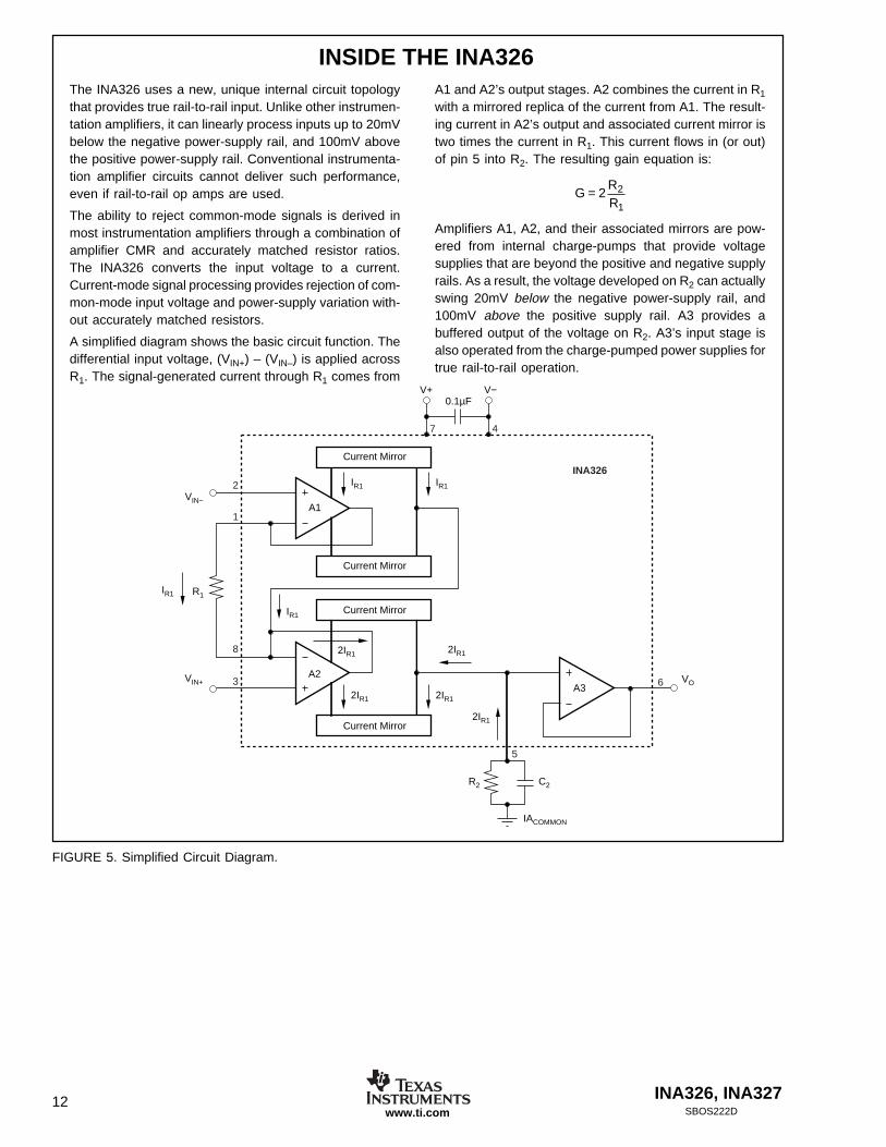
The INA326 uses a new, unique internal circuit topologythat provides true rail-to-rail input. Unlike other instrumen-tation amplifiers, it can linearly process inputs up to 20mVbelow the negative power-supply rail, and 100mV abovethe positive power-supply rail. Conventional instrumenta-tion amplifier circuits cannot deliver such performance,even if rail-to-rail op amps are used.
The ability to reject common-mode signals is derived inmost instrumentation amplifiers through a combination ofamplifier CMR and accurately matched resistor ratios.The INA326 converts the input voltage to a current.Current-mode signal processing provides rejection of com-mon-mode input voltage and power-supply variation with-out accurately matched resistors.
A simplified diagram shows the basic circuit function. Thedifferential input voltage, (VIN+) – (VIN–) is applied acrossR1. The signal-generated current through R1 comes from
A1 and A2’s output stages. A2 combines the current in R1
with a mirrored replica of the current from A1. The result-ing current in A2’s output and associated current mirror istwo times the current in R1. This current flows in (or out)of pin 5 into R2. The resulting gain equation is:
GRR
= 2 2
1
Amplifiers A1, A2, and their associated mirrors are pow-ered from internal charge-pumps that provide voltagesupplies that are beyond the positive and negative supplyrails. As a result, the voltage developed on R2 can actuallyswing 20mV below the negative power-supply rail, and100mV above the positive supply rail. A3 provides abuffered output of the voltage on R2. A3’s input stage isalso operated from the charge-pumped power supplies fortrue rail-to-rail operation.
FIGURE 5. Simplified Circuit Diagram.
INSIDE THE INA326
A1
V+ V−
Current Mirror
Current Mirror
IR1
IR1
IR1 R1
R2 C2
VO
VIN−
VIN+
IR1
2IR1
2IR1 2IR1
2IR1
2IR1
A3A2
IACOMMON
0.1µF
Current Mirror
Current Mirror
7 4
6
5
3
8
1
2
INA326

INA326, INA327 13SBOS222D www.ti.com
FIGURE 6. Generating Output Offset Voltage.
R1
R′2
5
R0
R2 C2
C0VREF
VO
G = 2 (R2 || R′2)/R1
INA326
R2 and R′2 are chosen to create a small output offset voltage (e.g., 100mV).Gain is determined by the parallel combinationof R2 and R′2.
2
1
8
3
6
FIGURE 7. Output Referenced to VREF/2.
2kΩ
200kΩ
200kΩ
VREF
RO100Ω
5
6
2
1
8
3
CO1µF
C2
INA326A/D
Converter
G = 2(200kΩ || 200kΩ)/2kΩ = 100
FIGURE 8. High-Side Current Shunt Measurement.
INA326
+5V
RL
5
2
1
8
3
6
7 RO100Ω
RS
IL
R1
2kΩ
R2 C2
VO
CO1µF
NOTE: Connection pointof V+ will include ( ) or exclude ( ) quiescent current in the measurementas desired. Output offsetrequired for measurements near zero (see Figure 6).
RS must be chosenso that the input voltagedoes not exceed 100mV beyond the rail.
VO = 2(IL × RS)R2
R1
APPLICATION CIRCUITS

INA326, INA32714SBOS222Dwww.ti.com
FIGURE 10. Low-Side –48V Current Shunt Monitor.
INA326
RL
IL
5
4
2
1
8
3
6
7
RI = 2kΩ 0.1µF
OPA336PA
1nF
+5V
76
2
VCC
GND
34
RF = 100kΩ
RSTART100kΩ
RPULL- DOWN200kΩ
VO = 2(IL × RS)
8.45kΩ
ZMM5231BDICT5.1V
ZVN4525G(zetex)
(High- Voltage n- Channel
FET)
RSVS = 0mVto 50mV max
−
+
−48V
NOTE: 0.2% accuracy. Current shunt monitor circuit can be designed for −250V supplywith appropriate selection of high- voltage FET.
RF
RI
FIGURE 11. High-Side +48V Current Shunt Monitor.
INA326
Load
5
7
2
1
8
3
6
4
7
2
3
6
4
RI2kΩ
OPA336PA
1nF
0.1µF
49.9kΩ
75kΩ
165kΩ
VO = 0.1V to 4.9V
8.45kΩ
ZMM5231BDICT5.1V
RSHUNT
VSHUNT = 0mVto 50mV
−
++48V
VCC
GND
(High- Voltage p- Channel FET)
ZVP4525(zetex)
+5V
FIGURE 9. Low-Side Current Shunt Measurement.
INA326
+5V
RL
RS
IL
RO100Ω
5
2
1
8
3
67
C2
CO1µF
2kΩ
VO
R2
R1
NOTE: Connection point of V− will include ( ) orexclude ( ) quiescent current in the measurementas desired. Output offset required for measurements near zero (see Figure 6).
RS must be chosen so thatthe input voltage does notexceed 20mV beyond the rail.
VO = 2(IL × RS)R2
R1

INA326, INA327 15SBOS222D www.ti.com
FIGURE 15. Programmable ±25µA Current Source with HighOutput Resistance.
FIGURE 12. Output Offset Adjustment.
2kΩ
100kΩ1nF
5
VO = VIN (100) + VDAC
VDAC = 0.075Vto 4.925V
INA326
2
1
8
3
6
DAC
+
−
VIN
INA326
45
72
1
8
3
6
RF = 10k
NOTE: Output resistance is typically 800MΩ.Resolution < 5nA. Recommended values of CF = 1nF to 1µF.
+5V
CF
VREF = +2.5V
R1200kΩ
DAC IOUT = ((+VREF) − (VDAC))
R1 ± 50nA
0V < VDAC < +5V
FIGURE 14. Output from Pin 5 to Allow Swing Beyond the Rail.
INA326
+5V
NC(1)
VO
+15V
−15V
OPA277
VD
C2R2
R1
VCM
5
6
72
1
8
34
4
672
3(2)
NOTES: (1) NC denotes No Connection.(2) Typical swing capability −20mV to (+5V + 100mV).
FIGURE 13. Multiplexed Output.
INA327
4
7
96
2
1
10
3
8R1
R3
R5
+5V
Enable
NOTE: (1) R2, R4, and R6 could be a single, shared resistor to save board space.
INA327
4
7
96
2
1
10
3
8
R4(1)
R2(1)
+5V
Enable
INA327
4
7
96
2
1
10
3
8
R6(1)
+5V
Enable
+1.8V to +5V
Logic
VO
1nF
1nF
1nF

INA326, INA32716SBOS222Dwww.ti.com
FIGURE 16. Programmable ±5mA Current Source.
FIGURE 17. ±27V Output at 200mA Amplifier with 100µV Offset.
INA326
45
72
1
8
3
6
IO = ±5mA with 0.1µA stability.
+2.5V
−2.5V
IO
0.1µF
VREF = +2.5V
RI = 200kΩ
10kΩ49.9Ω
DAC
RLIOUT = 2
VREF − VDAC
200kΩ1 +
10kΩ49.9Ω
INA326
4
4
5
7
7
2
1
8
3
2
3
6
6
+5V
−30V
+30V
IB
10nF
2kΩ
1MΩ
RI = 1kΩ
20kΩ
VI
20kΩ
RF = 100kΩ
OPA551
Internal charge pump in the INA326 allows this node to swing 20mV below ground without a negative supply.
Offset of the high- voltage op amp is controlled by the INA326.
VO = –27V
VOS = –100µV at 200mA
G = − = −100V/VRF
RI
NOTES: (1) The OPA551 is a 60V op amp. (2) The INA326 does not require anegative supply to correct for negative VOS values from the high-voltage op amp.(3) Voltage offset contribution of IB (OPA551) is 100pA • 2kΩ = 0.2µV.

INA326, INA327 17SBOS222D www.ti.com
FIGURE 18. Single-Supply PID Temperature Control Loop.
VS
V−
V+
V−
V+
R19
100k
Ω
R20
5k‰
PO
T
R17
5kΩ
PO
T
R2
100k
Ω
RD
IFF
1MΩ
Dif
fere
nti
ato
r T
C:
100m
s to
1s
R1
100k
Ω
C8
0.1µ
F
R25
10kΩ
R22
10kΩR
2310
kΩ
R21
10kΩ
Pro
po
rtio
nal
Err
or
Am
plif
ier
Bia
s G
ener
ato
r
Lo
op
Gai
nA
dju
st
Set
Tem
p
Gai
n =
100
V/V
Inte
gra
tor
TC
: 1s
to
10s
1/4
OPA
4340
1/4
OPA
4340
1/2
OPA
2340
1/4
OPA
4340
1/4
OPA
4340
CIN
T1µ
FR
INT
10M
Ω
R18
10kΩ
R15
200Ω
R16
2kΩ
PO
T
C3
1nF
VB
IAS
VB
IAS
VB
IAS
VS
VS
VB
IAS
Com
mon
Out
put t
oT
EC
Driv
er
Com
mon
+5V
Inpu
t
VB
IAS
VB
IAS
CD
IFF
1µF
Su
mm
ing
Am
plif
ier
INA
326
VO
6
R14
10kΩ
R13
20Ω
R10
1kΩ
C7
22nF
R8
100k
Ω
R9
2kΩ
R7
1kΩ
PO
T
R11
14.3
kΩ
R12
15kΩ RT
HE
RM
10k‰
R6
9.53
kΩ
C5
1nF
R5
20kΩ
R4
20kΩ
C2
470n
F
C6
10µF
RE
F10
04-
2.5
D1 7V+
4
0.1µ
F
V− 5
88 4 1
IN+
IN−
3 2
+
C4
10F
+
1/2
OPA
2340
VS
VS
C1
1nF
VB
IAS
PACKAGE OPTION ADDENDUM
www.ti.com 10-Jun-2014
Addendum-Page 1
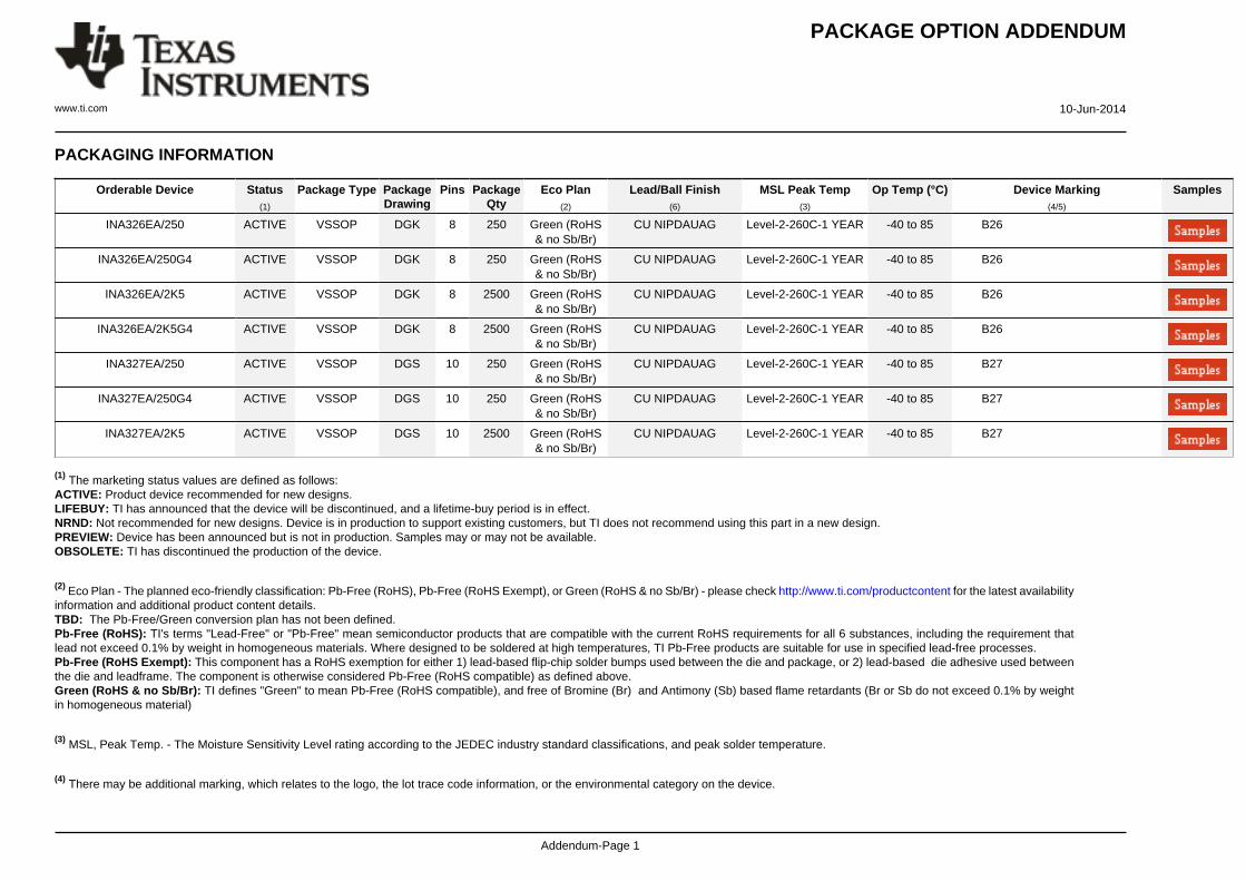
PACKAGING INFORMATION
Orderable Device Status(1)
Package Type PackageDrawing
Pins PackageQty
Eco Plan(2)
Lead/Ball Finish(6)
MSL Peak Temp(3)
Op Temp (°C) Device Marking(4/5)
Samples
INA326EA/250 ACTIVE VSSOP DGK 8 250 Green (RoHS& no Sb/Br)
CU NIPDAUAG Level-2-260C-1 YEAR -40 to 85 B26
INA326EA/250G4 ACTIVE VSSOP DGK 8 250 Green (RoHS& no Sb/Br)
CU NIPDAUAG Level-2-260C-1 YEAR -40 to 85 B26
INA326EA/2K5 ACTIVE VSSOP DGK 8 2500 Green (RoHS& no Sb/Br)
CU NIPDAUAG Level-2-260C-1 YEAR -40 to 85 B26
INA326EA/2K5G4 ACTIVE VSSOP DGK 8 2500 Green (RoHS& no Sb/Br)
CU NIPDAUAG Level-2-260C-1 YEAR -40 to 85 B26
INA327EA/250 ACTIVE VSSOP DGS 10 250 Green (RoHS& no Sb/Br)
CU NIPDAUAG Level-2-260C-1 YEAR -40 to 85 B27
INA327EA/250G4 ACTIVE VSSOP DGS 10 250 Green (RoHS& no Sb/Br)
CU NIPDAUAG Level-2-260C-1 YEAR -40 to 85 B27
INA327EA/2K5 ACTIVE VSSOP DGS 10 2500 Green (RoHS& no Sb/Br)
CU NIPDAUAG Level-2-260C-1 YEAR -40 to 85 B27
(1) The marketing status values are defined as follows:ACTIVE: Product device recommended for new designs.LIFEBUY: TI has announced that the device will be discontinued, and a lifetime-buy period is in effect.NRND: Not recommended for new designs. Device is in production to support existing customers, but TI does not recommend using this part in a new design.PREVIEW: Device has been announced but is not in production. Samples may or may not be available.OBSOLETE: TI has discontinued the production of the device.
(2) Eco Plan - The planned eco-friendly classification: Pb-Free (RoHS), Pb-Free (RoHS Exempt), or Green (RoHS & no Sb/Br) - please check http://www.ti.com/productcontent for the latest availabilityinformation and additional product content details.TBD: The Pb-Free/Green conversion plan has not been defined.Pb-Free (RoHS): TI's terms "Lead-Free" or "Pb-Free" mean semiconductor products that are compatible with the current RoHS requirements for all 6 substances, including the requirement thatlead not exceed 0.1% by weight in homogeneous materials. Where designed to be soldered at high temperatures, TI Pb-Free products are suitable for use in specified lead-free processes.Pb-Free (RoHS Exempt): This component has a RoHS exemption for either 1) lead-based flip-chip solder bumps used between the die and package, or 2) lead-based die adhesive used betweenthe die and leadframe. The component is otherwise considered Pb-Free (RoHS compatible) as defined above.Green (RoHS & no Sb/Br): TI defines "Green" to mean Pb-Free (RoHS compatible), and free of Bromine (Br) and Antimony (Sb) based flame retardants (Br or Sb do not exceed 0.1% by weightin homogeneous material)
(3) MSL, Peak Temp. - The Moisture Sensitivity Level rating according to the JEDEC industry standard classifications, and peak solder temperature.
(4) There may be additional marking, which relates to the logo, the lot trace code information, or the environmental category on the device.

PACKAGE OPTION ADDENDUM
www.ti.com 10-Jun-2014
Addendum-Page 2
(5) Multiple Device Markings will be inside parentheses. Only one Device Marking contained in parentheses and separated by a "~" will appear on a device. If a line is indented then it is a continuationof the previous line and the two combined represent the entire Device Marking for that device.
(6) Lead/Ball Finish - Orderable Devices may have multiple material finish options. Finish options are separated by a vertical ruled line. Lead/Ball Finish values may wrap to two lines if the finishvalue exceeds the maximum column width.
Important Information and Disclaimer:The information provided on this page represents TI's knowledge and belief as of the date that it is provided. TI bases its knowledge and belief on informationprovided by third parties, and makes no representation or warranty as to the accuracy of such information. Efforts are underway to better integrate information from third parties. TI has taken andcontinues to take reasonable steps to provide representative and accurate information but may not have conducted destructive testing or chemical analysis on incoming materials and chemicals.TI and TI suppliers consider certain information to be proprietary, and thus CAS numbers and other limited information may not be available for release.
In no event shall TI's liability arising out of such information exceed the total purchase price of the TI part(s) at issue in this document sold by TI to Customer on an annual basis.

TAPE AND REEL INFORMATION
*All dimensions are nominal
Device PackageType
PackageDrawing
Pins SPQ ReelDiameter
(mm)
ReelWidth
W1 (mm)
A0(mm)
B0(mm)
K0(mm)
P1(mm)
W(mm)
Pin1Quadrant
INA326EA/250 VSSOP DGK 8 250 330.0 12.4 5.3 3.4 1.4 8.0 12.0 Q1
INA326EA/2K5 VSSOP DGK 8 2500 330.0 12.4 5.3 3.4 1.4 8.0 12.0 Q1
INA327EA/250 VSSOP DGS 10 250 180.0 12.4 5.3 3.4 1.4 8.0 12.0 Q1
INA327EA/2K5 VSSOP DGS 10 2500 330.0 12.4 5.3 3.4 1.4 8.0 12.0 Q1
PACKAGE MATERIALS INFORMATION
www.ti.com 26-Jan-2013
Pack Materials-Page 1

*All dimensions are nominal
Device Package Type Package Drawing Pins SPQ Length (mm) Width (mm) Height (mm)
INA326EA/250 VSSOP DGK 8 250 366.0 364.0 50.0
INA326EA/2K5 VSSOP DGK 8 2500 366.0 364.0 50.0
INA327EA/250 VSSOP DGS 10 250 210.0 185.0 35.0
INA327EA/2K5 VSSOP DGS 10 2500 367.0 367.0 35.0
PACKAGE MATERIALS INFORMATION
www.ti.com 26-Jan-2013
Pack Materials-Page 2


IMPORTANT NOTICETexas Instruments Incorporated and its subsidiaries (TI) reserve the right to make corrections, enhancements, improvements and otherchanges to its semiconductor products and services per JESD46, latest issue, and to discontinue any product or service per JESD48, latestissue. Buyers should obtain the latest relevant information before placing orders and should verify that such information is current andcomplete. All semiconductor products (also referred to herein as “components”) are sold subject to TI’s terms and conditions of salesupplied at the time of order acknowledgment.TI warrants performance of its components to the specifications applicable at the time of sale, in accordance with the warranty in TI’s termsand conditions of sale of semiconductor products. Testing and other quality control techniques are used to the extent TI deems necessaryto support this warranty. Except where mandated by applicable law, testing of all parameters of each component is not necessarilyperformed.TI assumes no liability for applications assistance or the design of Buyers’ products. Buyers are responsible for their products andapplications using TI components. To minimize the risks associated with Buyers’ products and applications, Buyers should provideadequate design and operating safeguards.TI does not warrant or represent that any license, either express or implied, is granted under any patent right, copyright, mask work right, orother intellectual property right relating to any combination, machine, or process in which TI components or services are used. Informationpublished by TI regarding third-party products or services does not constitute a license to use such products or services or a warranty orendorsement thereof. Use of such information may require a license from a third party under the patents or other intellectual property of thethird party, or a license from TI under the patents or other intellectual property of TI.Reproduction of significant portions of TI information in TI data books or data sheets is permissible only if reproduction is without alterationand is accompanied by all associated warranties, conditions, limitations, and notices. TI is not responsible or liable for such altereddocumentation. Information of third parties may be subject to additional restrictions.Resale of TI components or services with statements different from or beyond the parameters stated by TI for that component or servicevoids all express and any implied warranties for the associated TI component or service and is an unfair and deceptive business practice.TI is not responsible or liable for any such statements.Buyer acknowledges and agrees that it is solely responsible for compliance with all legal, regulatory and safety-related requirementsconcerning its products, and any use of TI components in its applications, notwithstanding any applications-related information or supportthat may be provided by TI. Buyer represents and agrees that it has all the necessary expertise to create and implement safeguards whichanticipate dangerous consequences of failures, monitor failures and their consequences, lessen the likelihood of failures that might causeharm and take appropriate remedial actions. Buyer will fully indemnify TI and its representatives against any damages arising out of the useof any TI components in safety-critical applications.In some cases, TI components may be promoted specifically to facilitate safety-related applications. With such components, TI’s goal is tohelp enable customers to design and create their own end-product solutions that meet applicable functional safety standards andrequirements. Nonetheless, such components are subject to these terms.No TI components are authorized for use in FDA Class III (or similar life-critical medical equipment) unless authorized officers of the partieshave executed a special agreement specifically governing such use.Only those TI components which TI has specifically designated as military grade or “enhanced plastic” are designed and intended for use inmilitary/aerospace applications or environments. Buyer acknowledges and agrees that any military or aerospace use of TI componentswhich have not been so designated is solely at the Buyer's risk, and that Buyer is solely responsible for compliance with all legal andregulatory requirements in connection with such use.TI has specifically designated certain components as meeting ISO/TS16949 requirements, mainly for automotive use. In any case of use ofnon-designated products, TI will not be responsible for any failure to meet ISO/TS16949.Products ApplicationsAudio www.ti.com/audio Automotive and Transportation www.ti.com/automotiveAmplifiers amplifier.ti.com Communications and Telecom www.ti.com/communicationsData Converters dataconverter.ti.com Computers and Peripherals www.ti.com/computersDLP® Products www.dlp.com Consumer Electronics www.ti.com/consumer-appsDSP dsp.ti.com Energy and Lighting www.ti.com/energyClocks and Timers www.ti.com/clocks Industrial www.ti.com/industrialInterface interface.ti.com Medical www.ti.com/medicalLogic logic.ti.com Security www.ti.com/securityPower Mgmt power.ti.com Space, Avionics and Defense www.ti.com/space-avionics-defenseMicrocontrollers microcontroller.ti.com Video and Imaging www.ti.com/videoRFID www.ti-rfid.comOMAP Applications Processors www.ti.com/omap TI E2E Community e2e.ti.comWireless Connectivity www.ti.com/wirelessconnectivity
Mailing Address: Texas Instruments, Post Office Box 655303, Dallas, Texas 75265Copyright © 2014, Texas Instruments Incorporated