preliminary specification final product specification · 10.1 mechancal drawing 10.2 schematic...
TRANSCRIPT

R665101
Page 1 of 36
MODEL NO. : R665101
ISSUED DATE: 2019-4-28
VERSION : A0
■Preliminary Specification
□Final Product Specification
Customer :
Approved by Notes
Confirmed :
Prepared by Checked by Approved by
This technical specification is subjected to change without notice.

Page 2 of 36
Table of Contents
Table of Contents ............................................................................................................................ 2
Record of Revision .......................................................................................................................... 3
1 General Specifications ............................................................................................................. 4
2 Input/output Terminals .............................................................................................................. 5
2.1 Main FPC Pin Assignment .............................................................................................. 5 2.2 TP FPC Pin Assignment ................................................................................................. 6 2.3 Circuit block diagram (Display) ....................................................................................... 7 2.4 MCU and Display Module Interface Configuration .......................................................... 7
3 Absolute Maximum Ratings ...................................................................................................... 8
3.1 Driving AMOLED Panel .................................................................................................. 8 4 Electrical Characteristics .......................................................................................................... 8
4.1 Driving AMOLED Panel .................................................................................................. 8 5 AC Characteristics ................................................................................................................... 9
5.1 MIPI Interface Characteristics ........................................................................................ 9 5.2 Display RESET Timing Characteristics ......................................................................... 13 5.3 TE Timing Characteristics ............................................................................................ 14
6 Recommended Operating Sequence ..................................................................................... 16
6.1 Display Power on / off Sequence ................................................................................. 16 6.2 Brightness control ........................................................................................................ 16
7 Optical Characteristics Optical Specification .......................................................................... 10
8 Environmental / Reliability Test ............................................................................................... 23
9 Quality Level .......................................................................................................................... 24
9.1 AMOLED Module of Characteristic Inspection .............................................................. 24 9.2 Sampling Procedures for each item acceptance table .................................................. 24 9.3 Inspection Item ............................................................................................................. 25
10 Mechanical Drawing ............................................................................................................... 25
10.1 Mechancal Drawing 10.2 Schematic Diagram 11 Precautions for Use of AMOLED Modules .............................................................................. 36
11.1 Handling Precautions: .................................................................................................. 36 11.2 Storage Precautions: .................................................................................................... 36 11.3 Transportation Precautions: ......................................................................................... 36
R665101

Page 3 of 36
Record of Revision
Rev Issue Date Description Editor
A0 2019-04-28 Preliminary WEI YU
R665101

Page 4 of 36
1 General Specifications
Feature Spec Remark
Display
Spec
Screen Size (inch) 6.65
Display Mode AMOLED
Resolution(dot) 1080(W)×2340(H)
Active Area(mm) 70.78(W)×153.36 (H)
Pixel Pitch (um) 65.54 (W)×65.54(H)
Technology Type LTPS
Color Depth 16.7M
Interface MIPI 4LANE
Surface Treatment HC
Mechanical
Characterist
ics
With TP/Without TP With TP(on Cell)
Module Outline
Dimension(W x H x D)
(mm)
72.58(W)x156.36(H)x0.93(D)
Weight (g) 19.57±2.5g
Electronic
Driver IC(Type) R66455
Touch IC(Type) GT9886
Note 1: Requirements on Environmental Protection: RoHS 2.0.
R665101
Page 5 of 36
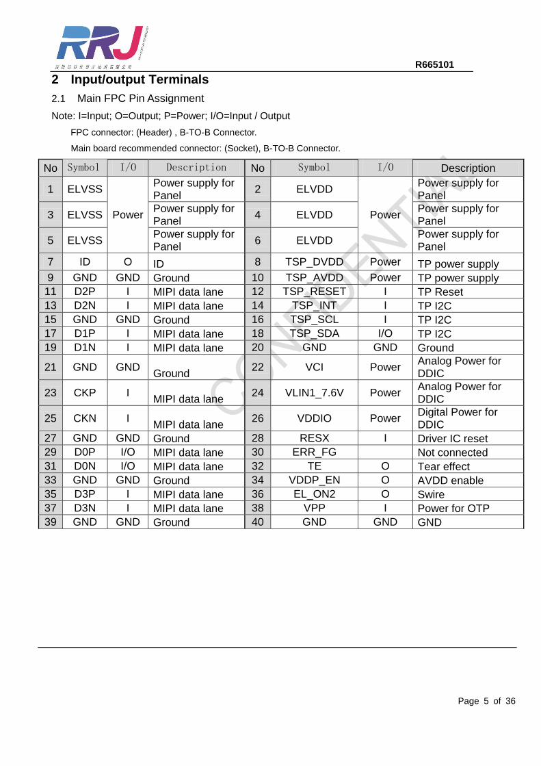
2 Input/output Terminals
2.1 Main FPC Pin Assignment
Note: I=Input; O=Output; P=Power; I/O=Input / Output
FPC connector: (Header) , B-TO-B Connector.
Main board recommended connector: (Socket), B-TO-B Connector.
No Symbol I/O Description No Symbol I/O Description
1 ELVSS
Power
Power supply for Panel
2 ELVDD
Power
Power supply for Panel
3 ELVSS Power supply for Panel
4 ELVDD Power supply for Panel
5 ELVSS Power supply for Panel
6 ELVDD Power supply for Panel
7 ID O ID 8 TSP_DVDD Power TP power supply
9 GND GND Ground 10 TSP_AVDD Power TP power supply
11 D2P I MIPI data lane 12 TSP_RESET I TP Reset
13 D2N I MIPI data lane 14 TSP_INT I TP I2C
15 GND GND Ground 16 TSP_SCL I TP I2C
17 D1P I MIPI data lane 18 TSP_SDA I/O TP I2C
19 D1N I MIPI data lane 20 GND GND Ground
21 GND GND Ground
22 VCI Power Analog Power for DDIC
23 CKP I MIPI data lane
24 VLIN1_7.6V Power Analog Power for DDIC
25 CKN I MIPI data lane
26 VDDIO Power Digital Power for DDIC
27 GND GND Ground 28 RESX I Driver IC reset
29 D0P I/O MIPI data lane 30 ERR_FG Not connected
31 D0N I/O MIPI data lane 32 TE O Tear effect
33 GND GND Ground 34 VDDP_EN O AVDD enable
35 D3P I MIPI data lane 36 EL_ON2 O Swire
37 D3N I MIPI data lane 38 VPP I Power for OTP
39 GND GND Ground 40 GND GND GND
R665101

Page 6 of 36
2.2 TP FPC Pin Assignment
No Symbol I/O Description
1 TSP_AVDD_3.3V P Analog Power for TP
2 NC / /
3 GND GND Ground
4 TSP_INT I Interrupt signal for TP
5 TSP_SDA I/O SDA pin for TP
6 TSP_SCL I SCL pin for TP
7 TSP_RESET I Reset Pin for TP, Active low.
8 TE I TE Pin for TP
R665101

Page 7 of 36
2.3 Circuit block diagram (Display)
2.4 MCU and Display Module Interface Configuration
VBAT
AVDD VCI VDDIO
Power Block
MIPI Interface
I2C
Power Block
Display
TSP
ELVDD
ELVSS
VCI
VDDIO
AVDD
DKN
DKP
DN[3:0]
DP[3:0]
RESX
GND
TP_SCL
TP_SDA
TP_INT
GND
TP_AVDD
TP_VDDIO
TP_RESET
R665101

Page 8 of 36
3 Absolute Maximum Ratings
3.1 Driving AMOLED Panel
Maximum Ratings (Voltage Referenced to VSS) Vss=0V, Ta=25℃
Item Symbol MIN MAX Unit
Analog Power supply VCI -0.3 +6.5 V
Logic Power supply VDDIO -0.3 +4.0 V
Positive Power Input ELVDD - +5.0 V
Negative Power Input ELVSS -5.4 - V
TP power supply Input TSP_AVDD -0.3 4.2 V
TP power supply for logic circuits
TSP_DVDD -0.3 4.2 V
Note: Functional operation should satisfy the limits in the Electrical Characteristics tables or Pin
Description section. If the module exceeds the absolute maximum ratings, permanent damage may occur.
Besides, if the module is operated with the absolute maximum ratings for a long time, the reliability may also
drop.
4 Electrical Characteristics
4.1 Driving AMOLED Panel Item Symbol MIN TYP MAX Unit
Logic Power supply VDDIO 1.65 1.80 3.6 V
Analog Power supply VCI 2.7 2.80 3.60 V
AVDD Supply Voltage AVDD 5.0 - 8.0 V
ELVDD Supply Voltage ELVDD 4.6 4.60 4.65 V
ELVSS Supply Voltage ELVSS -3.05 -3 - V
TP power supply Input TSP_AVDD 2.7 3.3 3.4 V
TP power supply for logic circuits
TSP_DVDD - 1.8 - V
Input Signal Voltage
High Level VIH 0.80*VDDIO - VDDIO V
Low Level VIL 0.00 - 0.20*VDDIO V
Output Signal Voltage
High Level VOH 0.80*VDDIO - VDDIO V
Low Level VOL 0.00 - 0.20*VDDIO V
Normal
IELVDD /IELVSS - 263 - mA
IVCI - 1 - mA
IVDDIO - 68 - mA
Iavdd - 32 - mA
Stand-by IVCI - 2 10 uA
IVDDIO - 5 20 uA
R665101

Page 9 of 36
Normal
(totol:
spec: 2.35 w,
max: w)
WELVDD - 2000 - mW
WELVSS - 2000 - mW
IVCI - 3 - mW
IVDDIO - 123 - mW
Iavdd - 224 - mW
Stand-by(totol:
spec: mw,
max: mw)
IVCI - 6 28 uw
IVDDIO - 9 36
uw
Ta=25℃
Note1: The input digital voltage is the I/O reference voltage.
Note2: VDDIO usually ranges from 1.65V to 3.6V. If VDDIO is changed, the remaining voltage
needs to be changed to the same voltage as VDDIO.
Note3: Under full white pattern, Command Mode 90Hz.
5 AC Characteristics
5.1 MIPI Interface Characteristics HS Data Transmission Burst
HS clock transmission
A
R665101

Page 10 of 36
Turnaround Procedure
Bus turnaround (BAT) from MPU to display module timing
Timing Parameters:
MIPI D-PHY characteristic
R665101

Page 11 of 36
MIPI D-PHY HS-RX clock and data-clock specifications
MIPI D-PHY LP-RX/TX clock and data-clock specifications
R665101

Page 12 of 36
R665101

Page 13 of 36
5.2 Display RESET Timing Characteristics Reset input timing:
VDDIO=1.65 to 3.6V, VDD=2.7 to 3.6V, AGND=DGND=0V, Ta=-40 to 85℃
Timing Parameters
Note. See a custom datasheet appendix for details of “Power On/Off sequence”. In addition, tRT1
specification depends on custom power configuration.
R665101

Page 14 of 36
5.3 TE Timing Characteristics
TELOM = 0: The TE output line consists of V-blanking information only. The TE output line is high during the vertical blanking period.
R665101

Page 15 of 36
TELOM=1,The TE ouput line consist of both V-blanking and H-blanking information
Tvdh = The display is not updated from the frame memory. Tvdl = The display is updated from the frame memory.
R665101
Page 16 of 36
6 Recommended Operating Sequence
6.1 Display Power on / off Sequence
6.1.1 Power On Sequence
6.1.2 Power Off Sequence
6.2 Brightness control Use “command 5100h, data xxh” to adjust the Manual Brightness value of the display:
In principle relationship is that 00h value means the lowest brightness and 0FFFh value means the highest brightness.
Inst/Para R/W Address
Date Type Description MIPI Other
BRTCTRL W 51h 5100h Hex Value form
0~4095(0FFF)
R665101

Page 17 of 36
6.3 TP Power on Sequence
TBD
R665101
Page 18 of 36
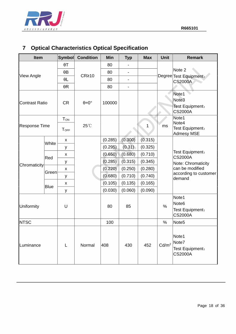
7 Optical Characteristics Optical Specification Item Symbol Condition Min Typ Max Unit Remark
View Angle
θT
CR≥10
80 -
Degree
Note 2
Test Equipment:CS2000A
θB 80 -
θL 80 -
θR 80 -
Contrast Ratio CR θ=0° 100000
Note1
Note3
Test Equipment:CS2000A
Response Time
TON
25℃ 1 ms
Note1 Note4
Test Equipment:Admesy MSE
TOFF
Chromaticity
White x
(0.285) (0.300) (0.315)
Test Equipment:CS2000A
Note: Chromaticity can be modified according to customer demand
y (0.295) (0.31) (0.325)
Red x (0.650) (0.680) (0.710)
y (0.285) (0.315) (0.345)
Green x (0.220) (0.250) (0.280)
y (0.680) (0.710) (0.740)
Blue x (0.105) (0.135) (0.165)
y (0.030) (0.060) (0.090)
Uniformity U 80 85 %
Note1
Note6
Test Equipment:CS2000A
NTSC 100 % Note5
Luminance L Normal 408 430 452 Cd/m2
Note1
Note7
Test Equipment:CS2000A
R665101

Page 19 of 36
Cross-talk 3.0 %
Note8
Test Equipment:CS2000A
Gamma 2.0 2.2 2.4
Note9
Gamma=2.2±0.2
Test Equipment:CS2000A
Test Conditions:
the ambient temperature is 25℃.
1. The test systems refer to Note1 and Note2.
2. Note 1: Definition of optical measurement system.
The optical characteristics should be measured in dark room. The optical properties are measured
at the center point of the AMOLED screen. All input terminals AMOLED panel must be ground
when measuring the center area of the panel.
Note 2: Definition of viewing angle range and measurement system.
Fig. 1 Definition of viewing angle
R665101

Page 20 of 36
Note 3: Definition of contrast ratio
“White state “: A state where the AMOLED should be driven by Vwhite.
“Black state”: A state where the AMOLED should be driven by Vblack.
Note 4: Definition of response time
The response time is defined as the AMOLED optical switching time interval between “White” state
and “Black” state. Rise time (TON) is the time between photo detector output intensity changing
from 10% to 90%. And fall time (TOFF) is the time between photo detector output intensity changing
from 90% to 10%.
Note 5: Definition of color chromaticity (CIE1931)
Color coordinates are measured at the center point of AMOLED.
R665101
Page 21 of 36
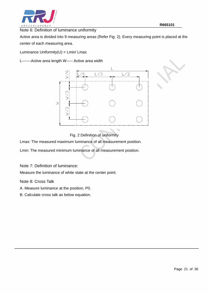
Note 6: Definition of luminance uniformity
Active area is divided into 9 measuring areas (Refer Fig. 2). Every measuring point is placed at the
center of each measuring area.
Luminance Uniformity(U) = Lmin/ Lmax
L-------Active area length W----- Active area width
Fig. 2 Definition of uniformity
Lmax: The measured maximum luminance of all measurement position.
Lmin: The measured minimum luminance of all measurement position.
Note 7: Definition of luminance:
Measure the luminance of white state at the center point.
Note 8: Cross Talk
A. Measure luminance at the position, P0.
B. Calculate cross talk as below equation.
R665101

Page 22 of 36
W1 W2 W3 W 4W _ OFF
B1 B2 B3 B4B_ OFF
Wi_ ON W _ OFF
W _ OFF
Bi_ ON B_ OFF
B_ OFF
L L L LL
4
L L L LL
4
|L L |crosstalk 100% (i 5 to 8)
L
|L L |crosstalk 100% (i 5 to 8)
L
Note9:Gamma
Form Gray200 to Gray255.,the spec is Gamma=2.1±0.4
.
R665101

Page 23 of 36
8 Environmental / Reliability Test
No Test Item Condition Remark
1 High Temperature Operation
+70℃, 240hrs According to the customer request
2 Low Temperature Operation
-20℃, 240hrs According to the customer request
3 High Temperature Storage
+80℃, 240hrs According to the customer request
4 Low Temperature Storage
-40℃, 120hrs According to the customer request
5 High Temperature & High Humidity Operation
60℃, 90% RH,240hrs According to the customer request
7 Thermal Shock (Non-operation)
-40℃(60 min)~+80℃(60 min),
Change time:5min, 24Cycles According to the customer request
8 Electro Static Discharge (Operation)
C=150pF, R=330Ω,7 points/panel
Air:±8KV, 5times; Contact:±4KV, 5 times;
(Environment: 15℃~35℃,
30%~45%, 86Kpa~106Kpa).
IEC61000-4-2 GB/T17626.2
R665101

Page 24 of 36
9 Quality Level
9.1 AMOLED Module of Characteristic Inspection
The environmental condition and visual inspection shall be conducted as below:
(1) Ambient temperature: 23± 3℃
(2) Humidity: 55 ± 10%RH
(3) Ambient light intensity of visual inspection: 800 ~ 1300 lux
(4) Ambient light intensity of function inspection: ≤200lux
(5) Viewing Distance: 30 ± 5cm
(6) Viewing angle (tolerance): the front side 45° (Z) ±15°
(7) Inspection time: 10 ±5 sec
(8) Time:10S~15S
9.2 Sampling Procedures for each item acceptance table
Defect type Sampling Procedures AQL
Major defect
GB/T2828.1-2003 Inspection levelⅡ
normal inspection
single sample inspection
0.65
Minor defect
GB/T2828.1-2003 Inspection levelⅡ
normal inspection
single sample inspection
0.4
Major defect: Any defect may result in functional failure, or reduce the usability of product for its purpose. For example, electrical failure, deformation and etc.
Minor defect A defect does not reduce the usability of product for its intended purpose and un-uniformity, such as dot defect and etc. The criteria on major and/or minor judgment will be according with the classification of defects.
目视角度
R665101

Page 25 of 36
9.3 Inspection Item
No Item Area Criterion of Defect Defect type
1 Dot Defect AA
Type DS
Acceptable number(A)
Minor Bright Dot ≥10mm 0
Dark Dot ≥10mm 2
Dark Dot(≥two
connections) ≥10mm 0
2 No Display AA / Not allowed Major
3 Abnormal Display
AA / Not allowed Major
4
Normally white(Unable
to switch screen)
AA / Not allowed Major
5
Line Defect
(Bright/Dark
) AA / Not allowed Major
6 ELA Mura AA 8% ND standard (under white V64 screen) Major
7 Color & Edge
Mura AA See limit sample(under full white screen ) Minor
8 Ipad air、
Color shift AA See limit sample(under full white screen ) Major
9 Water Ripple AA Not allowed Minor
10
Other mura (Water
stain、Low
gray-scale mura、S-
Line Mura)
AA 8% ND standard (under white V64 screen) Major
11 TP AA TP function NG Not allowed Major
12 Cover
edge/side breakage
Position
Z X(mm) Y(mm)
Acceptable number(A)
Major
≤3
Lead area ≤t ≤5 ≤0.4
R665101

Page 26 of 36
Chipping ≤t ≤2 ≤0.4
Edge Chipping
≤t ≤1 ≤1
13 Screen
sawtooth
Ink screen printing
W(mm) Acceptable
number(A)
Minor W≤0.05 Ignore
W>0.05 Not allowed
CG Edge
CG edge cutting sawtooth Not allowed
Edge drop paint Reference limit sample
14 Glass crack Full area / Not allowed Major
15
Line defects of
appearance vision
(scratches,
burrs, etc.)
AA area and whole
visible area of
cover lens
W(mm) L(mm)
DS(mm
)
Acceptable number
(A)
Minor W≤0.03 - - Ignore
0.03<W≤0.05 L≤2.0 ≥10 2
0.05<W - - 0
- L>2.0 - 0
16
Line defects of light vision(scratches,
burrs, etc.)
AA
W(mm) L(mm)
DS(mm
)
Acceptable number
(A)
Minor W≤0.02 L≤3.0 - Ignore
0.02<W≤0.03 L≤1.0 - 1
0.03<W - - 0
- L>1.0 - 0
17 convex point Whole area
/ Not allowed Major
18 Dirty fit AA According to the dotted line standard, if
necessary reference limit sample. Reference
limit sample Minor
19 UV glue
Not IC side
Over coating Not allowed Minor
IC side The coating of IC side is not higher than POL.
20
Point defects of
appearance vision
(Panel/Cov
er lens concave, black and white dots,
Visible surface
D(mm) DS(mm)
Acceptable number(A)
Minor D≤0.1 ≥5 Ignore
0.1<D≤0.2 ≥10 2
0.2<D - 0
R665101
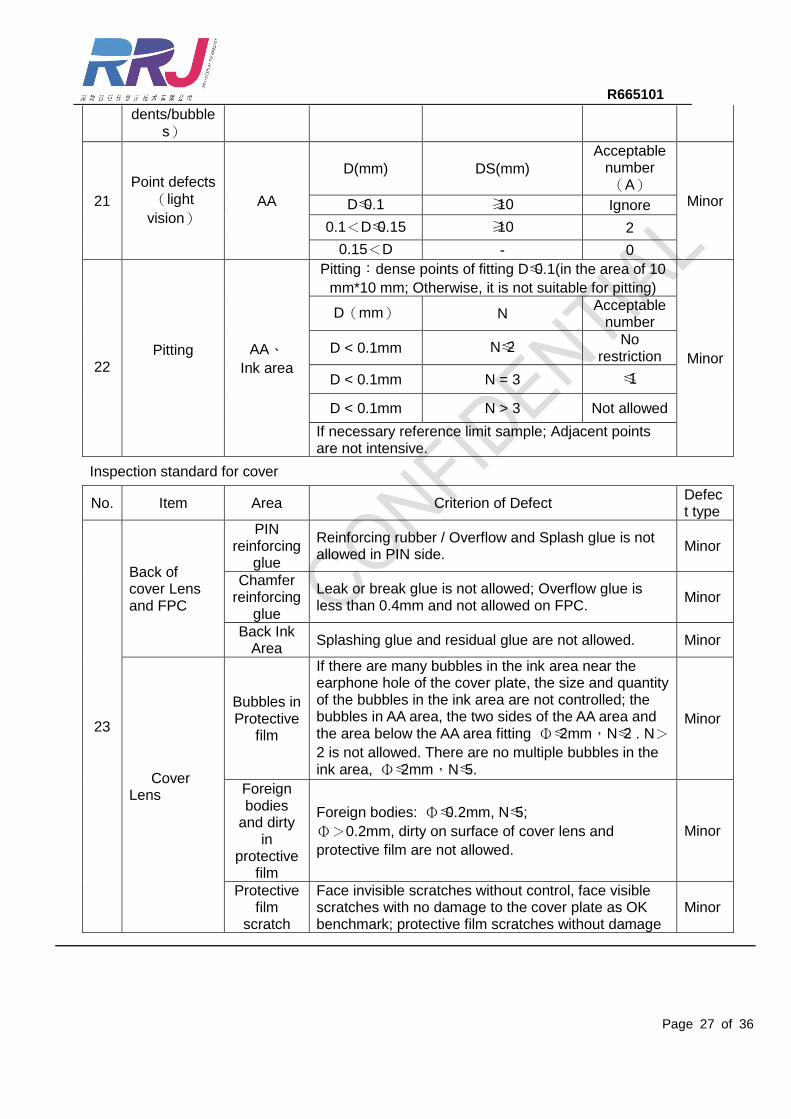
Page 27 of 36
dents/bubble
s)
21
Point defects
(light
vision) AA
D(mm) DS(mm)
Acceptable number(A)
Minor D≤0.1 ≥10 Ignore
0.1<D≤0.15 ≥10 2
0.15<D - 0
22
Pitting
AA、
Ink area
Pitting:dense points of fitting D≤0.1(in the area of 10
mm*10 mm; Otherwise, it is not suitable for pitting)
Minor
D(mm) N Acceptable
number
D < 0.1mm N≤2 No
restriction
D < 0.1mm N = 3 ≤1
D < 0.1mm N > 3 Not allowed
If necessary reference limit sample; Adjacent points are not intensive.
Inspection standard for cover
No. Item Area Criterion of Defect Defect type
23
Back of cover Lens and FPC
PIN reinforcing
glue
Reinforcing rubber / Overflow and Splash glue is not allowed in PIN side.
Minor
Chamfer reinforcing
glue
Leak or break glue is not allowed; Overflow glue is less than 0.4mm and not allowed on FPC.
Minor
Back Ink Area
Splashing glue and residual glue are not allowed. Minor
Cover Lens
Bubbles in Protective
film
If there are many bubbles in the ink area near the earphone hole of the cover plate, the size and quantity of the bubbles in the ink area are not controlled; the bubbles in AA area, the two sides of the AA area and the area below the AA area fitting Φ≤2mm,N≤2 . N>
2 is not allowed. There are no multiple bubbles in the ink area, Φ≤2mm,N≤5.
Minor
Foreign bodies
and dirty in
protective film
Foreign bodies: Φ≤0.2mm, N≤5;
Φ>0.2mm, dirty on surface of cover lens and
protective film are not allowed.
Minor
Protective film
scratch
Face invisible scratches without control, face visible scratches with no damage to the cover plate as OK benchmark; protective film scratches without damage
Minor
R665101
Page 28 of 36
to the cover plate without control, without control of the print.
Protective film
Deviation
Protective film attachment deviation≤0.4mm Minor
Appearance defects of cover lens
No cover scratches, light leakage, bumps, long windows teeth, missing teeth, dislocation caused by uneven ink are allowed.(If necessary reference limit
sample.)
Minor
heterogeneous color of cover lens
No heterogeneous color of cover lens around ICON Within 2mm. Other limited samples can refer to temporary limited samples.
Minor
small protective film dirt in the two side of receiver hole on cover lens
Discolored and mass dirt are not allowed. Minor
White cover lens with 2.5D Arc Edge white Line
Refer to limited samples. Minor
24 Hearing Hole and Key Hole
Residual glue
Not allowed Minor
25 IR hole
Ink unevenne
ss and mura
Not allowed.(If possible, reference limit samples.)
Minor
Foreign bodies
and dirty The wiped dirty is not allowed.
Dot defects
D≤0.15mm,N≤1, Not visible on black background.
Line defects
W≤0.03mm,L≤1mm,N≤1,Not visible on black
background.
Scratched
W≤0.03mm,L≤1mm,N≤1,Not visible on black
background. Transmittance test for scratched products, NG is not allowed
Backside small
protective film
The small protective film attached on the back of the IR hole does not cover the IR hole completely, and the edge of the protective film can not be exposed in the front view.
Residual glue
Not allowed.
R665101

Page 29 of 36
transmission rate
Under 850um condition, the transmittance of IR hole is more than 77%.
26 Camera Hole
Abnormal substance、dirt
If the problem is found, transmission test shall be carried out. Cleaning dirt is not allowed.
Minor
Residual adsorbent
ring Not allowed.
Dot Defect D≤0.1mm, and N≤1. Point defects cannot be located
in the middle. No discoloration is allowed.
line defect Not allowed
Backside small
protective film
The small protective film attached on the back of the camera hole does not cover the camera hole completely, and the edge of the protective film can not be exposed in the front view.
27
ICON
chromatic aberration
If possible, reference limit samples.
Minor
Dot defect D≤0.1mm, and N≤1. Point defects cannot be located
in the middle. No discoloration is allowed.
line defect Not allowed
28 Insulating
tape Compone
nt area
Components should be fully covered. Insulating tape should not exceed 2 mm of FPC edge or offset 2 mm from top to bottom of designated attachment area.
Minor
29 Compound adhesive
tape LTPS
No breakage, no light leakage, no influence on formation, no influence on thickness, no leakage sticking, from the Encap surface can not exceed the edge of the screen.
Minor
30 ACF Bonding area
The length of attachment is more than both ends of FPC, which should be range from 0.2 to 1mm.
Minor
31 ACF Bonding Bubble and Indentation
Bonding Area
The indentation is controlled by OK sampling limit. The bubble area is less than 1/2 of a single PAD, without overlapping two PADs, and the whole exhaust bubble length at the end of the positioning hole is less than 1/3 of that of the PAD.
Major
32 FPC after bonding
FOF Arch Height
FOF Arching Height < 0.7mm Major
FPC after folding
For the height control of FPC bending zone, see the process drawings of the module. Thickness(CG TO
TP FPC):< 2.85, thickness (CG TO Driver
FPC):<2.20. FPC folds back and attaches back
side and lifting height is less than 0.5mm.
Minor
R665101

Page 30 of 36
33 FPC Skew Bonding
area Not allowed Major
34 FPCA FPC
The component can not reverse polarity
Major
No wrong insertion
FPC should not have serious crease which destroy the line, prick and spots damage. Hard scratches of length ≥ 2mm are not allowed, based on the absence
of copper, the injured line is not allowed;
FPC does not allow corner area ≥ 2mm * 2mm;
FPC does not allow edge damage length or depth ≥
1mm
Minor
The gold fingers should not be oxidized, scraped, folded, impressed, broken, spotted or dissymmetry.
Major
Make sure FPC is not scalded, with its location holes not having deficiency or obviously shift.
Major
The component of FPC should be the same as BOM list.
Major
FPC two-dimensional code leak printing is not allowed. The printing is blurred but the readable code is OK.
Major
No remaining soldering Sn or Residual gum Major
No visual particle on the pad line Minor
Broken or defective copper foil is not allowed (width greater than 1/4 width)
Minor
35 Connect Connector noumenon
There should be no tin on the connector and no tin on the solder foot of the connector.
Minor
36 Package Other
It is not allowed to be mouldy, wet, and damaged, and not allowed to be mixed. ROHS tags need to be attached.
Major The positive and negative sides of the product can be wiped by themselves and dirt is not allowed.(Deliverable products such as A);
Products should put into the anti-static trays, with non-overlapping, and the trays should be staggered placed.
Minor Material codes, specifications, models, quantities, weights, production dates, batches and versions must be clearly identified.
Repair items must be marked with "Repair items" on the outer case and have a repair report.
R665101
Page 31 of 36
If there is any special material, the bar code of Nubia requirement should be affixed as required.
Note: If some product specifications are not clearly defined, they are not allowed to be controlled.
R665101

R665101
泡棉上
铜箔在
客户
端需
接地
Component Area Max:H=1.15mm(含锡
)Component Area Max:H=1.00mm(含
锡)
导电
布0.05mm-XPHF1R03-050D
IC点胶溢
胶范
围0.6mm
(不可高于
IC高度
)
PIN DESCRIPTION
40GND
39GND
38D3N
37
36D3P
35ELON2
34GND
33VDDP_EN
32D0N
31TE
30D0P
29ERR_FG
28GND
27RESX
26CKN
25VDDI
24CKP
23VLIN1_7.6V
GND21
VCI_3.3V
20D1N
19GND
18D1P
17TSP_SDA
16GND
15TSP_SCL
14D2N
13TSP_INT
12D2P
11TSP_RESET
10GND
9TSP
_AVDD_3.0V
8ID(GND)
7
6ELVSS
5ELVDD
4ELVSS
3ELVDD
2ELVSS
1ELVDD
VPP(MTP POWER)
TSP_DOVDD_1V8
补强
板区
域
87
65
4
FEDCBA
65
4
32
1
FEDCB
3
A
21
ASSY-Outline
7
Notes:1.Display Mode:6.65 inch OLED,正
向扫描
;2.Driver IC: R66455;3.TP IC: GT9886;4.储
存温
度: -30~80℃
,操作温度: -20~70℃
;5.Module FPC Connector:
OK-14M024-04公座;
AA
LTPS Glass
Encap
LTPS Glass
AA
COF上的
导电
布
含导电布
不含
保护膜
厚度
10 Drawing
10.1 Module Mechanical Drawing

Page 33 of 36
10.2 Tp Fpc Drawing
R665101

Page 34 of 36
10.3 Driver Fpc Drawing
R665101
Page 35 of 36
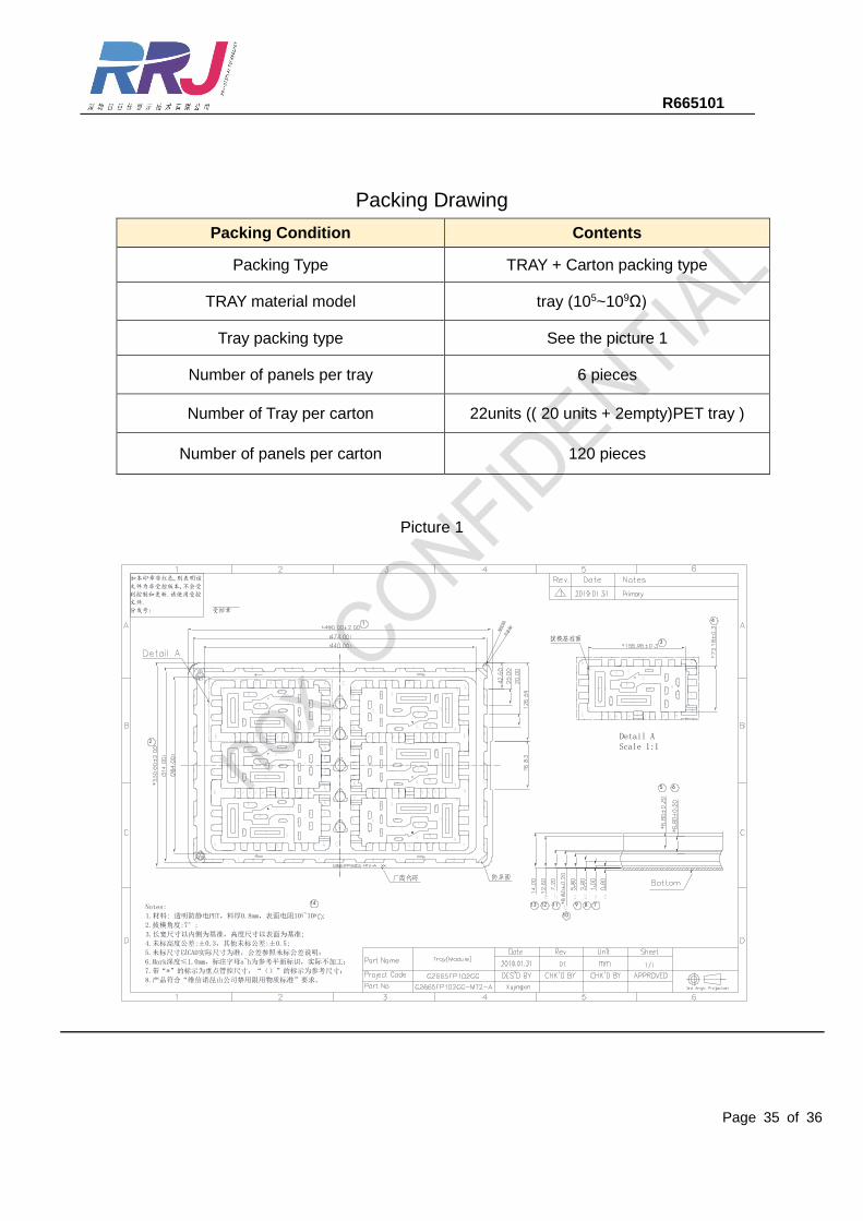
Packing Drawing
Picture 1
如本印章非红色,则表明该
文件为非受控版本,不会受
到控制和更新.请使用受控
文件.
分发号: 受控章
7
5
Detail AScale 1:1
8
6
9
10
1213
1
11
2
3
4
Notes:
1.材料: 透明防静电PET,料厚0.8mm,表面电阻105~109 ;
2.拔模角度:7°;
3.长宽尺寸以内侧为基准,高度尺寸以表面为基准;
4.未标高度公差:±0.3,其他未标公差:±0.5;
5.未标尺寸以CAD实际尺寸为准,公差参照未标公差说明;
6.Mark深度≤1.0mm,标注字母a~h为参考平面标识,实际不加工;
7.带“*”的标示为重点管控尺寸,“()”的标示为参考尺寸;
8.产品符合“维信诺昆山公司禁用限用物质标准”要求。
14
Packing Condition Contents
Packing Type TRAY + Carton packing type
TRAY material model tray (105~109Ω)
Tray packing type See the picture 1
Number of panels per tray 6 pieces
Number of Tray per carton 22units (( 20 units + 2empty)PET tray )
Number of panels per carton 120 pieces
R665101
Page 36 of 36
11 Precautions for Use of AMOLED Modules
11.1 Handling Precautions: 11.1.1 The display panel is made of glass. Do not subject it to a mechanical shock by dropping it
from height. 11.1.2 Do not press down the screen on the adjoining areas too hard because the color tone may
be shifted. 11.1.3 The polarizer covering the display surface of the AMOLED module is soft and easily
scratched. Handle this polarizer carefully. 11.1.4 If the display surface is contaminated, blow on the surface and gently wipe it with a soft
dry cloth. If it is still not completely clear, moisten the cloth with ethyl alcohol. 11.1.5 Solvents may damage the polarizer. Do not use water, ketone or aromatic solvents except
ethyl alcohol. Do not attempt to disassemble the AMOLED Module. 11.1.6 If the logic circuit power is off, do not apply the input signals. 11.1.7 To prevent destruction from static electricity, be careful to maintain an optimum working
environment. 11.1.8 Be sure to make yourself in contact with the ground when handling with the AMOLED
Modules. 11.1.9 Tools required for assembly, such as soldering irons, must be properly ground. 11.1.10 To reduce the generation of static electricity, do not conduct assembly or other work under
dry conditions. 11.1.11 To protect the display surface, the AMOLED Module is coated with a film. Be careful when
peeling off this protective film, because static electricity may generate.
11.2 Storage Precautions: 11.2.1 When storing the AMOLED modules, be sure that they are not directly exposed to the
sunlight or the light of fluorescent lamps. 11.2.2 The AMOLED modules should be stored under the storage temperature range. If the
AMOLED modules will be stored for a long time, the recommended condition is: Temperature: 0℃~40℃ Relatively humidity: ≤80%
11.2.3 The AMOLED modules should be stored in the room without acid, alkali or harmful gas.
11.3 Transportation Precautions: 11.3.1 The AMOLED modules should not be suffered from falling and violent shocking during
transportation. Besides, excessive press, water, damp and sunshine, should be avoided.
R665101