presentazione standard di powerpoint - nereid · – rectenna = rectifying antenna – matching...
TRANSCRIPT

1
Energy Management
Trends in micro-power conversion and management
for energy harvesting applications
Aldo ROMANI
Department of Electrical, Electronic, and
Information Engineering “Guglielmo Marconi”
Advanced Research Center on Electronic
Systems “E. De Castro”
Campus of Cesena, University of Bologna
2
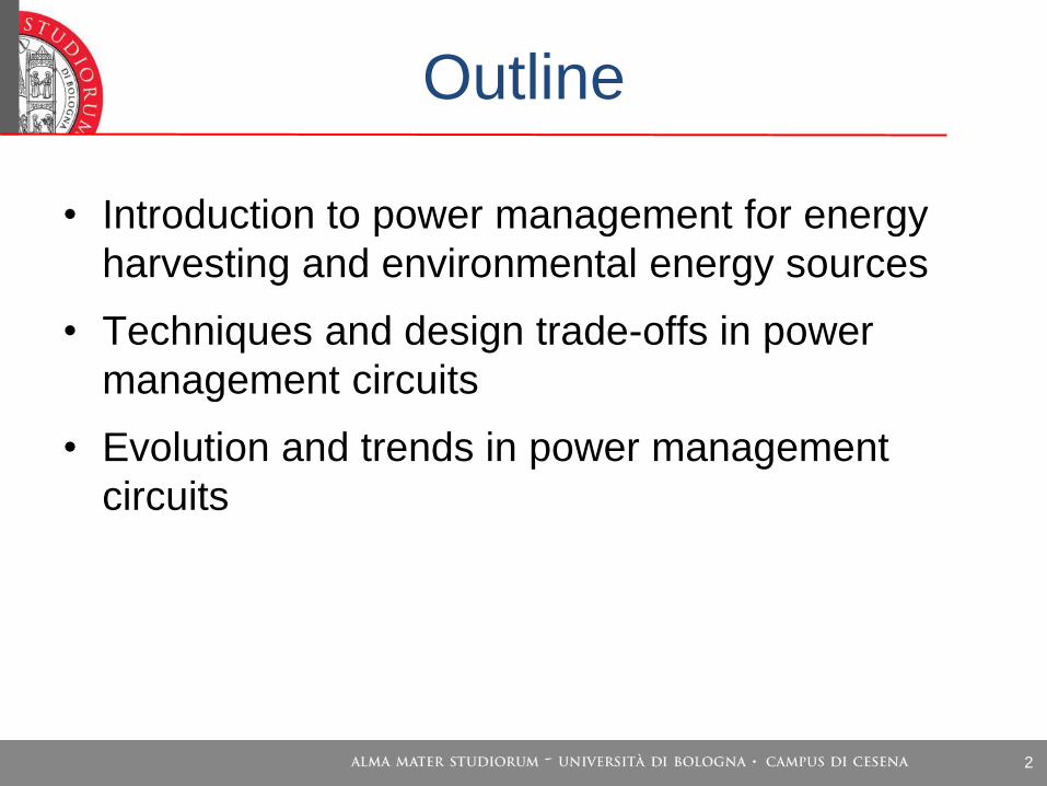
Outline
• Introduction to power management for energy
harvesting and environmental energy sources
• Techniques and design trade-offs in power
management circuits
• Evolution and trends in power management
circuits

3
Introduction to energy
harvesting

4
Market Trends
• The energy harvesting market is growing slower than predicted
– Power from miniature source is actually very low, in the order of µW
– Larger batteries are still cheaper than energy transducers
– Applications and circuits (sensors, RF transceivers, power converters, etc.)
are thought for operating with batteries and not in extreme power- and
voltage- constrained scenarios
Value of EH devices by applicationValue of EH devices by application
4500
5000 Other+
Healthcare#
3500
4000Military and aerospace excluding WSN
Other Industrial^
Wireless sensor mesh networks
2500
3000
$ m
illi
on
Other portable consumer electronics~
Mobile phones
Laptops and e-books
1500
2000
Va
lue U
S$
Bicycle dynamo
Wristwatches
0
500
1000
Consulting – Publications – Conferences © IDTechEx Ltd
0
2010 2011 2012 2013 2014 2015 2016 2017 2018 2019 2020
IDTechEx, Energy Harvesting Europe 2010 EETimes, 2016

5
The Bad
0
50
100
150
200
250
300
350
+0 +5 +10
Wh
/Kg
Years
Energy Storage Sources Projections
Li Ion
PEM Fuel Cell
• Gene’s law does not apply to analog sensing and transmission (slower decrease) • Energy storage density increases only ~1.5x/decade (~1.04x/year)
Energy autonomous systems: future trends in
devices, technology, systems, CATRENE Working
Group on Energy Autonomous Systems, 2009

6
The Good
The energy per bit per computation decreases according to the technology trend
(Gene’s law: energy/bit ~1.6x/year)
G. Frantz, Digital signal processor
trends, IEEE Micro, vol. 20, no. 6,
pp.52-59, 2000
(G. Frantz, SoC in the new Paradigm of IC technology, IEEE Consumer
Electronics Society – Dallas Chapter, Aug 2008)

7
Components of an
Energy Autonomous System
• Energy generation:
– Energy Harvesting: “transducers” making energy available from correlated or uncorrelated
sources of energy
– Energy Storage: Any kind of energy storage element that could be used to accumulate
energy in excess from the harvester (e.g. batteries, (super)capacitors, etc.)
• Energy conversion, management and distribution.
– any energy conversion system that trades and optimizes the energy flow from the Energy
Generation block, to the user load, from/to the energy storage
• Energy Consumption
– Data acquisition, elaboration, storage and transmission.
Energy
Harvesting
Energy
Storage
Power
Management
Ultra-low
Power
System
Energy generation Energy conversion,
management & distribution
Energy consumption
Energy autonomous system

8
Energy harvesting: what applications?
Body-powered devices:
Battery can be replaced with
PV cells, thermoelectric
generators that harvests
energy from light and human
body heat.
Smart clothing:
A small wearable antenna
collects energy from
electromagnetic waves
Smart shoes:
Vibrations can be used
for powering small
systems such as
wireless pedometer.
M.Dini et al., A fully
autonomous integrated
RF energy harvesting
system for wearable
applications, EuMW
2013
V. Leonov, C. Van
Hoof, R. Vllers,
Thermoelectric and
hybrid generators in
wearable devices
and clothes, BSN
2009, 6th Workshop
on Body Sensor
Networks,
N. Schenk, J.
Paradiso, Energy
scavenging with
shoe-mounted
piezoelectrics, Micro,
IEEE , vol.21, no.3,
2001

9
Energy harvesting: what applications?
• Smart home/cities/objects
• ‘True’ Internet-of-Things
• Roadmap towards trillion (connected)
sensors The ‘Abundance’
source: http://www.greenpeak.com
J. Bryzek, Emergence of Trillion Sensors
Movement, IEEE MEMS, 2014

10
Electromagnetic energy harvesters
• Perpetuum[1] energy harvester
– Frequency tuned on mains frequency 50/60 Hz BW<1Hz
– Output power up to 20 mW
– Diameter: 68 mm, height: 63.3 mm
• Enocean motion energy
harvester[2]
– Used for wireless light switches
– Dimensions: 29 x 19 x 7 mm3
– Energy output: 200 µJ @2V
• MEMS realizations[3]
– 0.1 cm3 volume
– 23 nW output power @1g @9.83 kHz
– electrodeposited copper coil
[1] Perpetuum Ltd.,
http://www.perpetuum.com
[2] Enocean, PTM200 Datasheet,
http://www.enocean.com
[3] S. Kulkarni et al., Design,
fabrication and test of integrated
micro-scale vibration-based
electromagnetic generator,
Sensors and Actuators A, vol.
145, 2008 (Tyndall Institute, Univ.
Southampton)
11
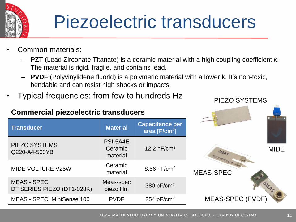
Piezoelectric transducers
• Common materials:
– PZT (Lead Zirconate Titanate) is a ceramic material with a high coupling coefficient k.
The material is rigid, fragile, and contains lead.
– PVDF (Polyvinylidene fluorid) is a polymeric material with a lower k. It’s non-toxic,
bendable and can resist high shocks or impacts.
• Typical frequencies: from few to hundreds Hz
Transducer Material Capacitance per
area [F/cm2]
PIEZO SYSTEMS
Q220-A4-503YB
PSI-5A4E
Ceramic
material
12.2 nF/cm2
MIDE VOLTURE V25W Ceramic
material 8.56 nF/cm2
MEAS - SPEC.
DT SERIES PIEZO (DT1-028K)
Meas-spec
piezo film 380 pF/cm2
MEAS - SPEC. MiniSense 100 PVDF 254 pF/cm2
PIEZO SYSTEMS
MIDE
MEAS-SPEC
MEAS-SPEC (PVDF)
Commercial piezoelectric transducers

12
RF Energy Harvesting
• RF carriers can be rectified in order to store locally energy
– Rectenna = rectifying antenna
– Matching network must be designed according to the expected
input power
• Simplified representation:
rectifier
output
capacitor
V-I and P-I transfer characteristics
several kΩ
typically few
hundreds mV

13
Micro-Thermoelectric Generators
Manufacturer - Product Size
[mm]
VOUT [V]
(matched
load)
PMAX [W]
(matched
load)
Power
density
[W/cm3/K]
Process
Eu. Thermodynamics -
GM200-449-10-12
WxL=54x57
H=3.8
11.4 @
ΔT=170K
14.6 @
ΔT=170K 7.34e-3 Standard
Eu. Thermodynamics -
GM200-127-10-15
WxL=30x30
H=3.7
4.14 @
ΔT=170K
2.72 @
ΔT=170K 4.80e-3 Standard
Nextreme - PG8005/6 WxL=11.2x10.2
H=1.1
0.85 @
ΔT=50K
0.13 @
ΔT=50K 2.07e-2 Thin film
Micropelt - MPG-D751 WxL=4.2x3.35
H=1.09
2.33 @
ΔT=30K
13.6e-3 @
ΔT=30K 2.96e-2 Thin film
GreenTEG – gTEG B* WxL=7.1x7.1
H=0.63
0.388 @
ΔT=37K
178e-6 @
ΔT=37K 1.51e-4 Thin film
ΔT is the temperature difference between
hot side (TH) and cold side (TC).
* Temperature difference between hot side
and ambient temperature. GreenTEG
Nextreme
Micropelt

14
Photovoltaic Energy Harvesting
Miniature commercial devices and emerging technologies
• Sanyo amorphous silicon PV cells (e.g. AM1407)
– Optimized for indoor fluorescent light (40-1000 Lux)
– Output power (AM-1407) ≈ 100 μW (indoor FL light, 240 Lux)
• Ixys© PV module in tiny SMD packages (e.g. CPC1822)
– Output power ≈ 100 μW at direct sunlight (6000 Lux)
• DSSC - Dye synthesized solar cell [1]
– Photoelectrochemical system (no silicon)
– Can be flexible and transparent
– Growing efficiency (up to 15% [2])
Sanyo AM1407
CPC1822 [1] Hardin, Brian E., Henry J. Snaith, and Michael D. McGehee.
"The renaissance of dye-sensitized solar cells." Nature
Photonics 6.3 (2012): 162-169.
[2] Burschka, Julian, et al. "Sequential deposition as a route to
high-performance perovskite-sensitized solar cells." Nature (2013).
equivalent circuit

15
Towards MEMS Energy Harvesters
• The current trend is to further shrink down energy
transducers thanks to MEMS technologies or wafer-level
processing (output power also scales!)
Electromagnetic
0.1 cm3, 23 nW @1g @9.83 kHz
electrodeposited copper coil
S. Kulkarni et al., Sensors and
Actuators A, vol. 145, 2008
(Tyndall Institute, Univ. Southampton)
Piezoelectric
200 nW @0.5g @400 Hz
16 mm2, deposited AlN
J. Iannacci et al., Microsystem
Technologies, vol. 20, 2014
(FBK, Delft Univ. Tech, Munich
Univ. Tech.)
Thermoelectric
6-20 mV/K, 2-10 W
3-9 mm2, 8-16 uW @1K
thin film semiconductor,
thermally conductive AlN
ceramics
Laird Technologies
eTEG

16
Current and Future Power Sources
1W
100 mW
10 mW
1 mW
100 µW
10 µW
1 µW
100 nW
10 nW
1 nW
solar panels, micro wind turbines,
miniature mechanical generators
(consolidated)
cm-sized energy harvesting
transducers: piezoelectric,
electromagnetic, thermoelectric, RF,
small-sized PV
(present)
MEMS devices, CMOS on-chip
photodiodes, microfabricated
thermoelectrics (mm-sized devices)
(near future)
bio-potentials, heart beat,
nanowires (piezo, PV, thermal)
(future?)

17
Techniques and design trade-offs for power
management circuits
Maximizing the
extracted power
18
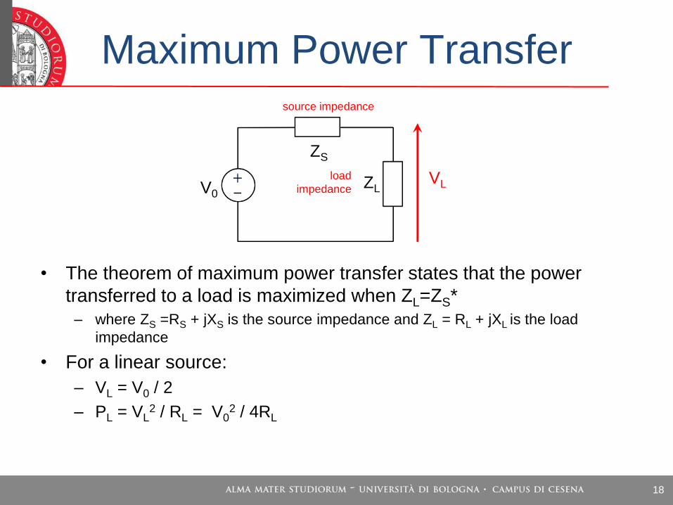
Maximum Power Transfer
• The theorem of maximum power transfer states that the power
transferred to a load is maximized when ZL=ZS*
– where ZS =RS + jXS is the source impedance and ZL = RL + jXL is the load
impedance
• For a linear source:
– VL = V0 / 2
– PL = VL2 / RL = V0
2 / 4RL
ZS
ZL V0
source impedance
load
impedance VL

19
Power Transfer Characteristics
• The I-V curves are a convenient way to describe the properties of a source in view of
the design of the power converter
– All curves combining two parameters among (P, V, I, RL) are equivalent: P=VI, V=RLI
• For a linear load, the MPP is located at 50% of V0
• For a PV cell, the MPP is located around 70-80% of V0
• In order to extract all the available power, a power converter should draw from the
source a current that keeps the actual voltage in proximity of the MPP
• I-V curves are also useful to estimate other features of the source (e.g. rise time, etc.)
I-V and P-V
curves for
linear sources
I-V and P-V
curves for a
PV source 50% V0 V0
ICC ICC
V0 75% V0

20
MPPT for DC sources • POUT depends on both the
source condition and on the
output current, and…
• …yes, there is a maximum!
(MPP).
• Fractional open-circuit
voltage MPPT technique (FOCV):
good compromise between power
spent and extracted – For each type of source the MPP roughly
occurs when the source voltage equals a
fixed fraction of the open-circuit voltage
(e.g. 75% for PV, 50% for linear sources)
– A DC/DC converter can switch so as to
keep the source around this voltage
– The reference voltage should be
periodically refreshed based on OCV
– …yes, it’s suboptimal but consumes little
energy
Sampling
open circuit
voltage
Energy
extraction
VIN
VOC
VREF
VIN
Optimum voltage

21
Piezoelectric Sources
• Let us now consider the simplified equivalent circuit of a piezoelectric transducer
• A rectifier is the simplest circuit for extracting power, but has limited and variable
efficiency
• If we apply the matched load (i.e., an unrealistically big L), power would seem to
be infinite (ideal voltage source)!
– NOTE: some parameters were neglected (series resistance, electromechanical
parameters, etc.). However, much higher power might still be available
simplified equivalent
circuit
efficiency
power transfer
characteristics
CP=50nF, CO=10µF,L=10mH,
R=10Ω,VP=5V,
22
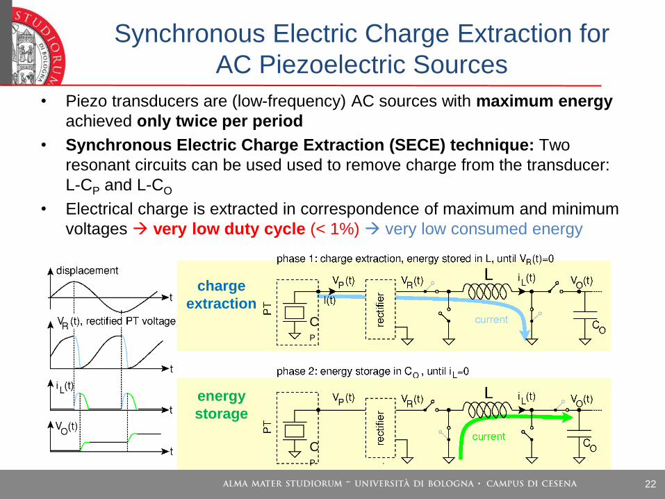
Synchronous Electric Charge Extraction for
AC Piezoelectric Sources
• Piezo transducers are (low-frequency) AC sources with maximum energy
achieved only twice per period
• Synchronous Electric Charge Extraction (SECE) technique: Two
resonant circuits can be used used to remove charge from the transducer:
L-CP and L-CO
• Electrical charge is extracted in correspondence of maximum and minimum
voltages very low duty cycle (< 1%) very low consumed energy
charge
extraction
energy
storage
CP
CP
23
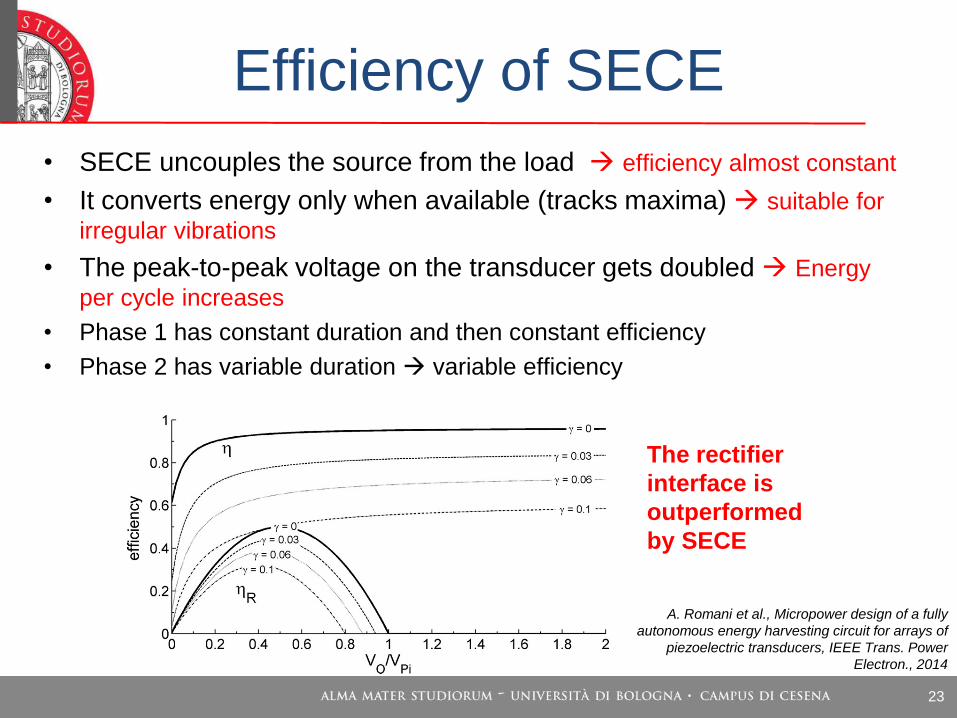
Efficiency of SECE
• SECE uncouples the source from the load efficiency almost constant
• It converts energy only when available (tracks maxima) suitable for
irregular vibrations
• The peak-to-peak voltage on the transducer gets doubled Energy
per cycle increases
• Phase 1 has constant duration and then constant efficiency
• Phase 2 has variable duration variable efficiency
A. Romani et al., Micropower design of a fully
autonomous energy harvesting circuit for arrays of
piezoelectric transducers, IEEE Trans. Power
Electron., 2014
The rectifier
interface is
outperformed
by SECE

24
Synchronized Switch Interfaces
• Synchronized-Switch Harvesting on Inductor (SSHI) consists in:
– an inductor L in series with an electronic switch connected in parallel with the piezoelectric element
– The electronic switch is briefly turned on when the mechanical displacement reaches a maximum or a minimum.
– The switch is turned off after a half electrical period, resulting in a quasi-instantaneous inversion of V.
• Many variations have been presented in literature E. Lefeuvre, et al., “A comparison between several vibration-powered
piezoelectric generators for standalone systems,” Sensors Actuators A, 2006.

25
PV
RF
TEG
PZ voltage
regulation
+ ext. load Romani et al.,
IEEE TPEL, 2014
Bandyopadhyay et al.,
JSSC 2012 Dini et al.,
IEEE TPEL 2015
FOCV
FOCV
FOCV
SECE
Multi-Source Harvesting Idea
• Micro-power conversion likely to
occur in discontinuous conduction
• A single time-shared inductor &
multi-input boost converter
1 SOURCE
2 SOURCES
N SOURCES
boost converter

26
Techniques and design trade-offs for power
management circuits
The importance of reducing
intrinsic power
27
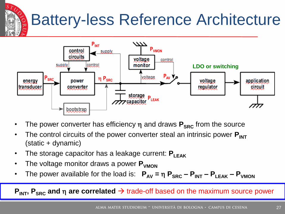
Battery-less Reference Architecture
• The power converter has efficiency h and draws PSRC from the source
• The control circuits of the power converter steal an intrinsic power PINT
(static + dynamic)
• The storage capacitor has a leakage current: PLEAK
• The voltage monitor draws a power PVMON
• The power available for the load is: PAV = h PSRC – PINT – PLEAK – PVMON
PINT, PSRC and h are correlated trade-off based on the maximum source power
PSRC
PINT
PLEAK
PVMON
h PSRC PAV
LDO or switching

28
Duty-cycled Operation
• When PLOAD > PAV duty-cycled operation is necessary
• The linear or switching regulator that supplies the load requires a minimum
voltage VDDL for operating
• Given the energy DE required by the load per activation, the maximum
voltage VDDH depends on CSTORE
• Large CSTORE large EBASE long wake-up time
• Small CSTORE higher VDDH higher PLEAK and PINT, less efficient regulation
• Trade-offs are generally required!
time
Vstorage
harvest
activate load
harvest
activate load
VDDH
VDDL
time
Vstorage
harvest
activate load
harvest
activate load
VDDH
VDDL
energy available
for the load
DE = ½ CSTORE (VDDH2-VDDL
2)
baseline energy
EBASE = ½ CSTORE VDDL2
useful range
unused range

29
Managing The Harvested Power
• Typical energy harvesting applications: when the power
consumed by the application is higher than the harvested power, the
duty-cycle of activation must be reduced
source:
ti.com
The average
consumed power
decreases with the
duty-cycle…
…at least, until we
reach the baseline
consumption
asymptotically!
Input power can be
lower than this!

30
Baseline Consumptions
• As duty cycle 0, the consumed power
approaches the ‘baseline’ consumption, i.e.:
1. The stand-by/sleep power of the
application circuits (e.g. CPU, radio, etc)
2. If the load supply is cut off, the static
current of the supervisor circuit (voltage
monitor)
3. In last instance, the intrinsic power of the power converter
• The hard limit for any energy harvesting application is the
intrinsic consumption of the power converter.
– the maximum source power must be necessarily higher in order to achieve
a positive power budget (i.e. to progressively store energy)
NOTE: keep in mind that if you want high h and also PSRC close to the MPP you’ll
generally have to spend higher PINT, but in power-constrained scenarios the
quantity to maximize is: PAV = h PSRC – PINT
31
Evolution & Trends in
Power Management Circuits
for Energy Harvesting
Applications

32
Advantages of ICs
• Why ASICs for energy harvesting?
– Very low parasitics and leakage currents extremely low intrinsic
power (at least 10x with respect to discrete components)
– Possibility of fine tuning of all design parameters
– Size is also reduced, but usually is not an issue (transducers, inductors
and storage are usually larger)
• What technology?
– No need for extreme integration: analog and power conversion circuits
do not benefit significantly from high miniaturization
– Older processes tend to handle higher voltages and have lower leakage
currents

33
Commercial devices
• The “Energy harvesting” words have been often
appearing in many datasheets in the last decade
• The first devices had still (relatively) high intrinsic
consumption limiting the efficiency
• Most of them were basically implementing a DC/DC
converter with an input rectifier for vibrational sources
• The next generation of devices implemented more
specific MPPT techniques for squeezing more power out
of the power source
• The latest generation target ultra-low intrinsic
consumption and look forward towards 1 µW operations

34
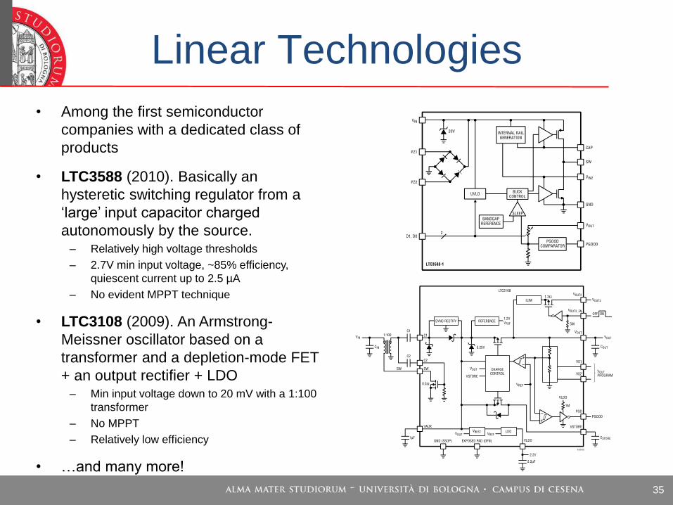
Linear Technologies
• Among the first semiconductor
companies with a dedicated class of
products
• LTC3588 (2010). Basically an
hysteretic switching regulator from a
‘large’ input capacitor charged
autonomously by the source. – Relatively high voltage thresholds
– 2.7V min input voltage, ~85% efficiency,
quiescent current up to 2.5 µA
– No evident MPPT technique
• LTC3108 (2009). An Armstrong-
Meissner oscillator based on a
transformer and a depletion-mode FET
+ an output rectifier + LDO – Min input voltage down to 20 mV with a 1:100
transformer
– No MPPT
– Relatively low efficiency
• …and many more!
35
Linear Technologies
• Among the first semiconductor
companies with a dedicated class of
products
• LTC3588 (2010). Basically an
hysteretic switching regulator from a
‘large’ input capacitor charged
autonomously by the source. – Relatively high voltage thresholds
– 2.7V min input voltage, ~85% efficiency,
quiescent current up to 2.5 µA
– No evident MPPT technique
• LTC3108 (2009). An Armstrong-
Meissner oscillator based on a
transformer and a depletion-mode FET
+ an output rectifier + LDO – Min input voltage down to 20 mV with a 1:100
transformer
– No MPPT
– Relatively low efficiency
• …and many more!

36
TI and STM • The TI bq255xx and the ST SPV1050
implement a buck-boost topology with
FOCV MPPT (16s refresh period)
– Best trade-off for minimizing intrinsic
consumption and for ULP sources
– Low voltage ‘cold’ start-up is performed
with internal charge pumps
– The ICs are supplied from the storage
device
• TI bq255xx
– cold start-up from 330mV and 15 µW
– sustained from 100 mV and 5 µW
– efficiency ~75%
– OCV sampling: 400 ms every 16 s
• ST SPV1050
– cold start-up from 550 mV
– sustained from 75 mV and 2.5 µW
– efficiency ~80%
– OCV sampling: 256 ms every 16 s
src: TI,
bq25570
datasheet
src: ST,
SPV1050
datasheet

37
ST SPV1050
• Typical operation Functional description SPV1050
18/36 DocID025569 Rev 4
Figure 6 shows the input voltage waveform of a PV panel supplying VOC = 1.25 V and
VMPP = 1.05 V.
Figure 6. MPPT tracking
Once the VEOC threshold is triggered, the switching of the DC-DC converter is stopped until
VSTORE will decrease to VEOC - EOCHYS.
Figure 7. Triggering of VEOC (BATT pin floating)
cold start-up FOCV sampling
source: SPV1050
datasheet

38
Meanwhile in scientific literature…
OTTMAN et al.: OPTIMIZED PIEZOELECTRIC ENERGY HARVESTING CIRCUIT 697
power of the piezoelectric element is the product of the output
current and the rectifier capacitor voltage
(2)
It is then apparent that the peak output power occurs when the
rectifier voltage is maintained at
(3)
or one-half the open-circuit voltage of the piezoelectric element.
The magnitude of the polarization current I generated by the
piezoelectric element, and hence the optimal rectifier voltage,
may not be constant as it depends upon the level and frequency
of the mechanical vibrations. This creates the need for flexi-
bility in the circuit, i.e., the ability to change the output voltage
of the rectifier as the mechanical excitation changes to achieve
and maintain the maximum power flow. To accomplish this, a
dc–dc step-down converter is placed between the rectifier and
the electronic load as shown in Fig. 1. A battery is used at the
output of the converter to provide energy storage and a “stiff”
voltage to power the electronic load. Control of the converter is
designed to maximize the power flow out of the converter and,
if effective, results in the piezoelectric element being at its point
of maximum power flow as described above.
The step-down converter is a natural choice for this appli-
cation, where the piezoelectric voltage can be very high and
reducing it to a level that is lower is required for the battery
and the electronic load. The analysis of the interaction between
the piezoelectric element and the step-down converter reveals a
simplified control scheme to achieve maximum power flow, al-
lowing the circuit to be self-powering while harvesting enough
energy for additional low-power electronic loads.
III. STEP-DOWN CONVERTER ANALYSIS
The maximum power transfer theory developed for the piezo-
electric element-rectifier circuit produced an expression for the
optimal rectifier voltage, (3). Regulation of this voltage, and
thereby the power flow from the piezoelectric element, is imple-
mented through adjustment of the step-down converter’s duty
cycle. The following analysis reveals that the power flow from
the piezoelectric element is maximized at an optimal duty cycle
and, as it departs from this optimal value, the output power drops
significantly.
Converter operation in DCM has been assumed in the fol-
lowing analysis and this reasoning will be discussed later in this
section. From [8], expressions for a step-down converter oper-
ating in DCM for the input—output voltage relationship and
output current are
(4)
(5)
Fig. 1. Energy harvesting circuitry.
where is the time period that the transistor is off and current
flows through the free-wheeling diode. (4) can be used to pro-
vide an expression for
(6)
and substituted into (5)
(7)
By conservation of power for the converter (assuming losses are
minimal), the output current can be expressed as a function of
the input voltage and current and output voltage
(8)
The input current of the converter can now be determined by
equating (7) and (8)
(9)
Substituting the output current of the piezoelectric device, (1),
as the input current to the converter and the rectifier capacitor
voltage as the voltage into the converter, (9) becomes
(10)
Solving (10) for the rectifier voltage
(11)
The input current to the converter can be determined as a func-
tion of the duty cycle by substituting (11) into (1)
(12)
Power produced by the piezoelectric element as regulated by the
converter can now be expressed as the product of the rectifier
voltage (converter input voltage) and the input current, (11) and
(12)
(13)
698 IEEE TRANSACTIONS ON POWER ELECTRONICS, VOL. 18, NO. 2, MARCH 2003
Which reduces to
(14)
The rectifier voltage and power flow from the piezoelectric ele-
ment as regulated by the step-down converter for any excitation
level, as specified by the magnitude of polarization current I ,
can now be determined.
For this circuit, the maximization of the power flow from
the piezoelectric element is considered as a function of the
step-down converter’s duty cycle. Solving (10) for the duty
cycle:
(15)
At peak power, the piezoelectric polarization current can be
found as a function of the optimal rectifier voltage from (3) as
(16)
Substituting into (15) and fixing the output voltage by the bat-
tery V , the optimal duty cycle which results in maximum
power can be determined as
(17)
This relationship, the optimal duty cycle and piezoelectric
element excitation level, is depicted in Fig. 2. For maximum
power transfer, the rectifier voltage is maintained at one-half the
open-circuit voltage (V being dependent on the mechanical
excitation); and as this voltage becomes much larger than the
output battery voltage, the optimal duty cycle approaches a
constant value. It is emphasized that this excitation/duty-cycle
relationship is for a step-down converter in DCM, and other
topologies or operating conditions would require different
analysis.
By assuming a sufficiently large converter input-to-output
voltage difference, the optimal duty cycle becomes relatively
constant and can be approximated as
(18)
The optimal duty cycle of the converter is thus dependent upon
its inductance and switching frequency, the piezoelectric ele-
ment’s capacitance, and the frequency of mechanical excitation
of the piezoelectric device.
Although the assumption of discontinuous conduction mode
yields the convenient conclusion of a relatively constant optimal
duty cycle at high excitation, the choice of this mode of
operation bears some discussion. Designing a converter to
always run in discontinuous conduction mode is questionable,
as the large ratio of RMS current to dc current in the inductor
and MOSFET will significantly increase conduction losses
as opposed to continuous conduction mode. However, for
low-power applications, DCM is often used even at full load
Fig. 2. Optimal duty cycle for maximum power transfer, step-down converter.
to avoid the reverse recovery problem of the diode [9], so the
power levels ( 50 mW) generated by the piezoelectric device
and the simplified control method justify this approach. We
also note that the above theory focused on the maximization of
input power rather than output power of the converter, which
would be more appropriate. Maximization of output power of
the converter, however, would require accurate loss models for
the converter components, and was not attempted in this work.
Provided the converter has reasonable efficiency, the optimal
operating points for maximizing input and output power of
the converter should be fairly close.
IV. CIRCUIT IMPLEMENTATION
Building upon the relationship between the optimal duty
cycle and the mechanical excitation, a dual method of energy
harvesting is proposed. At higher excitation levels of the piezo-
electric device, when the optimal duty cycle is nearly constant,
the step-down converter will operate at the fixed duty cycle
specified by (18). This allows for a simple controller consisting
of a fixed-duty-cycle pulse-width-modulated signal to drive the
switching MOSFET. Because the converter is only operated at
high excitations, two advantages are realized: first, the optimal
duty cycle is relatively fixed, so operation at the optimal power
point is ensured; and secondly, the higher excitations provide
sufficient energy to offset converter and control circuitry losses.
At lower excitations, the optimal duty cycle is still varying
substantially with the excitation, requiring a more complex,
adaptive control circuit with higher power consumption. An
initial study of the power levels in this range suggests har-
vesting would be marginal given even the lowest power control
circuitry [7]. Therefore, at lower excitations, the battery will
be charged by a pulse-charging circuit connected to the piezo-
electric element-rectifier circuit with the step-down converter
bypassed. The threshold level of mechanical excitation that
divides these two modes of operation will depend on several
criteria: the power produced by the piezoelectric element, the
losses of the step-down converter, the power consumption of
the control circuitry, and the optimal duty cycle stabilization at
higher excitations.
V. CIRCUIT DESIGN
A schematic of the step-down converter and the accompa-
nying control circuitry is shown in Fig. 3. The sub-circuits:
• 2003.G. Ottman et al., Optimized Piezoelectric energy harvesting
circuit using step-down converter in discontinuous conduction mode,
IEEE TPEL
• 2007. E. Lefeuvre et al., Buck-boost converter for sensorless power
optimization of piezoelectric energy harvester, IEEE TPEL – 85% efficiency with PIN 200 µW – 1.5 mW
• Similar approach as first product (rectifier + DC/DC)
39
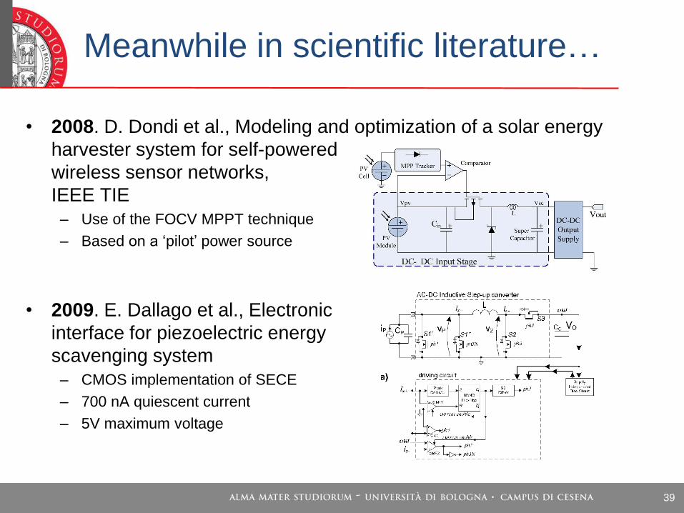
Meanwhile in scientific literature…
• 2008. D. Dondi et al., Modeling and optimization of a solar energy
harvester system for self-powered
wireless sensor networks,
IEEE TIE
– Use of the FOCV MPPT technique
– Based on a ‘pilot’ power source
• 2009. E. Dallago et al., Electronic
interface for piezoelectric energy
scavenging system
– CMOS implementation of SECE
– 700 nA quiescent current
– 5V maximum voltage
2760 IEEE TRANSACTIONS ON INDUSTRIAL ELECTRONICS, VOL. 55, NO. 7, JULY 2008
Fig. 1. Schematic diagram of the solar harvester.
adopted. Sections III and IV describe models of the PV module
and the harvester circuit, respectively. Section V describes
the circuit optimization methodology and provides some use-
ful guidelines for solar harvester design. Section VI presents
experimental results and a comparison between two different
solar harvester circuit implementations designed following the
proposed guidelines. Finally, Section VII concludes this paper.
II. SOLAR HARVESTING CIRCUIT
A. Circuit Architecture
The circuit architecture of the developed solar harvester is
presented in [12] and depicted in Fig. 1. It consists of three
main building blocks.
1) DC–DC Input Stage: Most of the MPPT systems pro-
posed in the literature employ standard switch-mode power
supply technologies, with switching transistors, diodes, and
capacitors. They are driven by a pulsewidth-modulated (PWM)
signal generated by a control algorithm. The three basic topolo-
gies are buck (step down), boost (step up), and buck–boost
(step up–down). In this implementation, a buck topology is
used to interface the voltage from the PV module to the SC.
The operation of the input dc–dc stage differs from the one of
a standard buck converter because input and output voltages do
vary during the SC charge process, as well as duty cycle, period,
and switching frequency of the MOSFET switch.
2) MPP Tracker: The MPP tracking is implemented by the
analog circuit highlighted in Fig. 1. It autonomously estimates
the MPP using an open-loop configuration without any in-
terference to the PV module. This way, the control unit is
simply implemented with a single low-power comparator that
compares the current PV module voltage to the estimated MPP
to generate the PWM control signal. No costly DSP or digital
controllers are necessary. The details of the generation of the
estimated MPP have been left out of the figure for the sake
of simplicity. The PWM control signal forces the pseudo-buck
dc–dc input stage to work within a narrow voltage window
centered on the MPP voltage Vmpp .
3) Output DC–DC Converter: The output dc–dc converter
delivering power supply to the wireless sensor node is required
to match the input voltage of the WSN node. This component
is not taken into account in this paper, because it needs cus-
tom design related to the operating voltage of the WSN node
adopted. Moreover, commercial integrated dc–dc converters
usually provide an efficiency on the order of 90%.
TABLE IMPP VOLTAGES MEASURED AND CALCULATED THROUGH (1)
CONSIDERING K FO C = 0.74 ON A WIDE RANGE
OF LIGHT CONDITIONS
The power supply for the harvester circuit is provided by
both the PV module and the output dc–dc power supply. This
design choice allows to improve the efficiency during the initial
phase of SC charging and enables the harvester circuit to start
operating when the SC voltage is low. For efficient harvester
operation, the MPP should continuously be tracked; hence, the
input stage and the comparator should also be powered when
the output dc–dc converter is off because the SC voltage is
below the start-up threshold. For this reason, the power supply
to the input MPPT stage is provided by the PV panel even when
the dc–dc converter is not operating.
B. MPPT Technique
There are several methods and algorithms to track the MPP
voltage [13]–[15]. The most popular ones are Perturb and
Observe (P&O) [13], [19] and Fractional Open-Circuit Voltage
(FOCV) [14], which is the one we adopted.
The P&O method is an approach that is widely used with
medium–high power PV modules, since it allows very accurate
MPP calculation. However, it requires complex control actions
that are often implemented using microcontrollers or DSPs. Al-
though analog versions are implemented, the main shortcoming
of this method is the high cost and complexity of the system.
On the other hand, FOCV is largely used in small-scale PV
systems. This method exploits the nearly linear relationship
between the operating voltage at MPP Vmpp of a PV module
and its open-circuit voltage VOC , i.e.,
Vmpp∼= K FOC ·VOC . (1)
K FOC is a constant that ranges from 0.71 to 0.78, which
slightly depends on irradiance conditions [1]. Considering
K FOC as a constant under different irradiance conditions leads
to small errors in the Vmpp evaluation but strongly simplifies
circuit solutions adopted to implement MPPT, also reducing
its power consumption. Table I reports that the maximum
difference between MPP voltages measured during PV panel
characterization (Vmpp ,meas) and calculated through (1) assum-
ing K FOC = 0.74(Vmpp ,cal ) [12] is smaller than 5% on a wide
range of light irradiance conditions.
VOC of small-size solar cells can be estimated by exploiting
sensing devices that autonomously monitor the environmental
light, such as light intensity sensors, voltage output sensors
Authorized licensed use limited to: UNIVERSITE LOUIS PASTEUR. Downloaded on November 26, 2009 at 07:02 from IEEE Xplore. Restrictions apply.
40
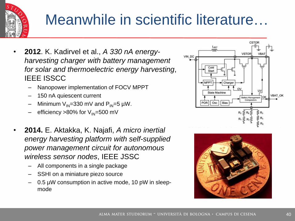
Meanwhile in scientific literature…
• 2012. K. Kadirvel et al., A 330 nA energy-
harvesting charger with battery management
for solar and thermoelectric energy harvesting,
IEEE ISSCC – Nanopower implementation of FOCV MPPT
– 150 nA quiescent current
– Minimum VIN=330 mV and PIN=5 µW.
– efficiency >80% for VIN=500 mV
• 2014. E. Aktakka, K. Najafi, A micro inertial
energy harvesting platform with self-supplied
power management circuit for autonomous
wireless sensor nodes, IEEE JSSC – All components in a single package
– SSHI on a miniature piezo source
– 0.5 µW consumption in active mode, 10 pW in sleep-
mode

41
Meanwhile in scientific literature…
• 2013-2015. M. Dini et al. (UNIBO), Developed a series of nanopower ASICs
for DC, piezoelectric, and heterogeneous energy harvesting sources, IEEE
TPEL, ESSCIRC, PRIME
• 2015-2016. A. Camarda et al. (UNIBO), developed an integrated ultra-low
voltage bootstrap circuit (15 mV) based on a piezoelectric transformer
• 2016. G. Chowdary et al., An 18 nA, 87%
efficient solar, vibration and RF
energy-harvesting power management
system with a single shared inductor,
IEEE JSSC
– Multi-source IC with single shared inductor
– PMIN = 25 nW, IDDq = 18 nA, 87% efficiency
0.32 µm STM technology
Multi-source (9 piezo&DC) with
independent MPPT and shared L
IDDq ≅ 360 nA (40 nA/source)
Efficiency up to 85%
0.32 µm STM technology
Implements SECE-RCI
Separate IC/load supplies
PMIN = 296 nW (@7 Hz,
0.5VPK)
0.32 µm STM technology
FOCV MPPT for DC srcs
Cold start-up @0.2V
Separate IC/load supplies
PMIN ≅ 1 µW, IDDq ≅ 300 nA
CHOWDARY et al.: AN 18 nA, 87% EFFICIENT SOLAR, VIBRATION AND RF ENERGY-HARVESTING POWER MANAGEMENT SYSTEM 2505
Fig. 5. Overall architecture of the chip.
where I P is the peak inductor current. The power absorbed by
the circuit is given by:
P = E/ TS =L I 2
P
2TS=
L I 2P IBI AS
VDCOSC(7)
where TS is the period of the oscillator, given by
VDCOSC/ 2IBI AS. The error in the power absorbed by the cir-
cuit because of a quantization error in the oscillator frequency
is given by:P
P= −
TS
TS= −
COSC
COSC. (8)
Equation (8) shows that the loss in efficiency (− P/ P) is the
relative quantization error ( COSC/ COSC). When we work
with a range of available powers, from 20 nW to 2 µW, the
value of COSC will adapt, according to our algorithm in Fig. 3,
to the available power. max(COSC) has to be designed for the
minimum power, i.e., 20 nW. If the number of calibration bits
in COSC is N, then the unit capacitor, C0 is max(COSC)/
(2N − 1), which is also equal to the quantization error in the
total value of the capacitor obtained. When the incident avail-
able power is 2 µW, the optimum value of COSC will decrease
to max(COSC) · 20 nW2 µW
. The relative quantization error (which
is also the efficiency loss according to (8)) at this power level
is now 100/ (2N − 1). With 9 bits, the lost efficiency because of
quantization error in the oscillator is < 20%. With additional
bits, the search process increases linearly, and the maximum
efficiency loss decreases exponentially.
III. ARCHITECTURE
A multi-source energy harvesting DC-DC buck-boost con-
verter controlled by oscillators, trained according to Fig. 3,
was designed. The goal was to harvest from available powers
ranging from 20 nW to 100 µW. The complete architecture
of the system is shown in Fig. 5. The system can be cold-
started through a photo-voltaic cell or an RF antenna, or
both (Fig. 5), to charge CD . Once VD goes above 1.2 V,
a VD-OK comparator (consuming 200 pW) having a hysteresis
of 0.16 V releases the VD-OK signal to start the search phase,
and disables start-up. When VD goes above 1.2 V, CD slowly
charges a large storage capacitor, Cstore (> 100 µF). When
Vstore goes above 1.3 V, Vstore-OK comparator goes high
and VD is shorted to Vstore. A search phase is also initiated.
A fraction of the OCV is sampled (VR) and a comparator,
U1, is used to initiate energize/dump pulses to regulate the
input voltage vB at VR. An oscillator is trained to mimic the
output of U1 in the digital controller. Once the oscillator is
trained, U1 is disabled and energize/dump signals are initiated
with the oscillator. The search phase is repeated after every

42
State of the art of nano-power PMICs
• S. Bandyopadhyay et al., A 1.1 nW energy
harvesting system with 544pW quiescent power
for next-generation implants, IEEE JSSC 2014
• Features
– 70-100 mV input from endo-cochlear bio-potential
inside ear
– Efficiency > 53% @ VDD=0.9V, L=47 uH
– Boost converter topology with
12 Hz switching frequency
– Trade-off between switching
frequency, FET sizes and power
losses carefully investigated
– 0.18 µm CMOS
– Cannot self-start
– The lowest intrinsic consumption
reported up to now
42

43
Trends: Commercial PMICs
1
10
100
0 1 2 3 4 5 6 7
Minim
uminputpower(µW)
Minimuminputvoltage(V)
• Two parameters
analyzed: minimum
start-up voltage
and minimum
input power
• Most effective
products target
today few µW and
few hundreds mV
power sources
• However, many
enviromental sources
often provide less than
that in their worst case
• No synchronized switch
harvesters for piezo
sources available up to now
44
0.001
0.01
0.1
1
10
100
0 1 2 3 4 5 6 7
Minim
uminputpower(µW)
Minimuminputvoltage(V)
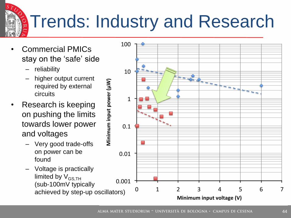
Trends: Industry and Research
• Commercial PMICs
stay on the ‘safe’ side
– reliability
– higher output current
required by external
circuits
• Research is keeping
on pushing the limits
towards lower power
and voltages
– Very good trade-offs
on power can be
found
– Voltage is practically
limited by VGS,TH
(sub-100mV typically
achieved by step-up oscillators)

45
0.001
0.01
0.1
1
10
100
0 1 2 3 4 5 6 7
Minim
uminputpower(µW)
Minimuminputvoltage(V)
Trends: Industry and Research
• Sub-µW operation is likely
to be achieved in commercial
PMICs in the near future
as market demands more
power efficient components
(MCUs, radios, analog front-
end for sensors, etc.)
• Ultra-low voltage circuits
are expected to stay in a
niche (lower efficiency and
higher min. power), with
a envisaged use for
battery-less circuit start-up
from fully discharged states

46
Conclusions

47
Conclusions
• Energy harvesting is an exciting research field experiencing
continuous advancements
• The micropower barrier was broken in research. Many commercial
power management ICs are becoming available. Careful designs can
yield to very interesting results
• Energy-aware and design techniques for operation in power-
constrained scenarios are progressively being applied to CPUs,
sensors, radios, etc. This is necessary to go further.

48
References • R.J.M. Vullers, R. Van Schaijk, I. Doms, C. Van Hoof, R. Mertens, Micropower energy harvesting, Solid. State. Electron. 53 (2009) 684–693. doi:10.1016/j.sse.2008.12.011.
• E. Lefeuvre, A. Badel, C. Richard, L. Petit, and D. Guyomar, “A comparison between several vibration-powered piezoelectric generators for standalone systems,” Sensors
Actuators A Phys., vol. 126, no. 2, pp. 405–416, Feb. 2006.
• J. Dicken, P. D. Mitcheson, I. Stoianov, and E. M. Yeatman, “Power-Extraction Circuits for Piezoelectric Energy Harvesters in Miniature and Low-Power Applications,” IEEE
Trans. Power Electron., vol. 27, no. 11, pp. 4514–4529, 2012.
• A. Dolgov, R. Zane, Z. Popovic, Power management system for online low power RF energy harvesting optimization, Circuits Syst. I Regul. Pap. IEEE Trans. 57 (2010)
1802–1811. doi:10.1109/TCSI.2009.2034891.
• T. Paing, R. Zane, Design and optimization of an adaptive non-linear piezoelectric energy harvester, in: 2011 Twenty-Sixth Annual. IEEE Appl. Power Electron. Conf. Expo.,
Ieee, 2011: pp. 412–418. doi:10.1109/APEC.2011.5744630.
• S. Boisseau, P. Gasnier, M. Gallardo, G. Despesse, Self-starting power management circuits for piezoelectric and electret-based electrostatic mechanical energy harvesters,
in: J. Phys. Conf. Ser., IOP Publishing, 2013: p. 012080. doi:10.1088/1742-6596/476/1/012080
• P. Gasnier, J. Willemin, S. Boisseau, G. Despesse, C. Condemine, G. Gouvernet, and J.-J. Chaillout, “An Autonomous Piezoelectric Energy Harvesting IC Based on a
Synchronous Multi-Shot Technique,” IEEE J. Solid-State Circuits, vol. 49, no. 7, pp. 1561–1570, Jul. 2014..
• A. Romani, M. Filippi, M. Dini, M. Tartagni, A sub-µA stand-by current synchronous electric charge extractor for piezoelectric energy harvesting, in: ACM J. Emerg. Technol.
Comput. 12(11) 2015
• E. Dallago, A.L. Barnabei, A. Liberale, P. Malcovati, G. Venchi, An Interface Circuit for Low-Voltage Low-Current Energy Harvesting Systems, IEEE Trans. Power Electron. 30
(2015) 1411–1420. doi:10.1109/TPEL.2014.2322521.
• K. Kadirvel, Y. Ramadass, U. Lyles, J. Carpenter, V. Ivanov, V. McNeil, et al., A 330nA energy-harvesting charger with battery management for solar and thermoelectric
energy harvesting, 2012 IEEE ISSCC (2012) 106–108. doi:10.1109/ISSCC.2012.6176896.
• M. Dini, A. Romani, M. Filippi, V. Bottarel, G. Ricotti, M. Tartagni, A Nano-current Power Management IC for Multiple Heterogeneous Energy Harvesting Sources, IEEE Trans.
Power Electron., vol.30, no.10, pp.5665,5680, Oct. 2015
• M. Dini, A. Romani, M. Filippi, M. Tartagni, "A Nano-Power Synchronous Charge Extractor IC for Low Voltage Piezoelectric Energy Harvesting with Residual Charge
Inversion," IEEE Trans. Power Electron., vol.PP, no.99, pp.1-1, Mar. 2015, ISSN: 0885-8993, DOI: 10.1109/TPEL.2015.2417352
• T. Hehn, F. Hagedorn, D. Maurath, D. Marinkovic, I. Kuehne, A. Frey, and Y. Manoli, “A Fully Autonomous Integrated Interface Circuit for Piezoelectric Harvesters,” Solid-
State Circuits, IEEE J., vol. 47, no. 9, pp. 2185–2198, 2012.
• E.E. Aktakka, K. Najafi, A Micro Inertial Energy Harvesting Platform With Self-Supplied Power Management Circuit for Autonomous Wireless Sensor Nodes, IEEE J. Solid-
State Circuits. 49 (2014) 2017–2029. doi:10.1109/JSSC.2014.2331953.
• S. Bandyopadhyay, P.P. Mercier, A.C. Lysaght, K.M. Stankovic, A. Chandrakasan, A 1.1nW energy harvesting system with 544pW quiescent power for next-generation
implants, in: 2014 IEEE Int. Solid-State Circuits Conf. Dig. Tech. Pap., IEEE, 2014: pp. 396–397. doi:10.1109/ISSCC.2014.6757485.
• M. Dini, A. Romani, M. Filippi, and M. Tartagni, “A Nano-Current Power Management IC for Low Voltage Energy Harvesting,” IEEE Trans. Power Electron., vol. 31, no. 6, pp.
4292–4304, 2016.

49
References • D. Masotti, A. Costanzo, P. Francia, M. Filippi, and A. Romani, “A Load-Modulated Rectifier for RF Micropower Harvesting With Start-Up Strategies,” IEEE Trans. Microw.
Theory Tech., 2014.
• A. Romani, M. Filippi, and M. Tartagni, “Micropower Design of a Fully Autonomous Energy Harvesting Circuit for Arrays of Piezoelectric Transducers,” IEEE Trans. Power
Electron., vol. 29, no. 2, pp. 729–739, Feb. 2014.
• T. Huang, C. Hsieh, Y. Yang, Y. Lee, Y. Kang, K. Chen, C. Huang, Y. Lin, and M. Lee, “A Battery-Free 217 nW Static Control Power Buck Converter for Wireless RF Energy
Harvesting With -Calibrated Dynamic On / Off Time and Adaptive Phase Lead Control,” IEEE J. Solid State Circuits, vol. 47, no. 4, pp. 852–862, 2012.
• [1] J. Kim, P. K. T. Mok, and C. Kim, “A 0.15 V Input Energy Harvesting Charge Pump With Dynamic Body Biasing and Adaptive Dead-Time for Efficiency Improvement,”
IEEE J. Solid-State Circuits, vol. PP, no. 99, pp. 1–12, 2014.
• G. Chowdary, A. Singh, and S. Chatterjee, “An 18 nA, 87% Efficient Solar, Vibration and RF Energy-Harvesting Power Management System With a Single Shared Inductor,”
IEEE J. Solid-State Circuits, vol. 51, no. 10, pp. 2501–2513, Oct. 2016.
• A. Camarda, A. Romani, E. Macrelli, and M. Tartagni, “A 32 mV/69 mV input voltage booster based on a piezoelectric transformer for energy harvesting applications,”
Sensors Actuators A Phys., May 2015.
• A. Romani, A. Camarda, A. Baldazzi, and M. Tartagni, “A micropower energy harvesting circuit with piezoelectric transformer-based ultra-low voltage start-up,” in 2015
IEEE/ACM International Symposium on Low Power Electronics and Design (ISLPED), 2015, pp. 279–284.
• Linear Technology, LTC3588 datasheet
• Linear Technology, LTC3108 datasheet
• TI, bq25570 datasheet
• STMicroelectronics, SPV1050 datasheet
• Cypress, S6AE10xA datasheet
• Cypress, MB39C811 datahseet
• Maxim, MAX17710 datashet

50
Thanks for your attention
The Energy Harvesting Team at
UNIBO – Campus of Cesena
Michele Dini
Post-doc researcher
Matteo Filippi
Research Assistant Antonio Camarda
Post-doc researcher
Rudi P. Paganelli
Researcher (CNR)
Marco Tartagni
Professor
Enrico Sangiorgi
Professor
Matteo Pizzotti
Ph.D. student

51
Aldo ROMANI Department of Electrical, Electronic, and Information Engineering “Guglielmo Marconi”
Advanced Research Center on Electronic Systems “E. De Castro”
University of Bologna, Campus of Cesena