principle of photovoltaic energy city – sehir university, istanbul – september 2013 dr mohamed...
TRANSCRIPT
Principle of Photovoltaic
Energy city – Sehir University, Istanbul – September 2013Dr Mohamed Zayed

Some references
• http://www.pveducation.org/• (a lot of info on photovoltaics and animations)
• MIT OpenCourseWare http://ocw.mit.edu (2.626 Fundamentals of Photovoltaics)
• http://www2.warwick.ac.uk/fac/sci/eng/staff/pad/teaching/lecture3.pdf(lecture on environment and photovoltaics)
• http://www.youtube.com/watch?v=z0mzusIoAk8(video introduction to photovoltaic)
• http://www.youtube.com/watch?v=bzcTFUcXwIY ( Martin Lorton video blog. Very instructive for house arrays application)
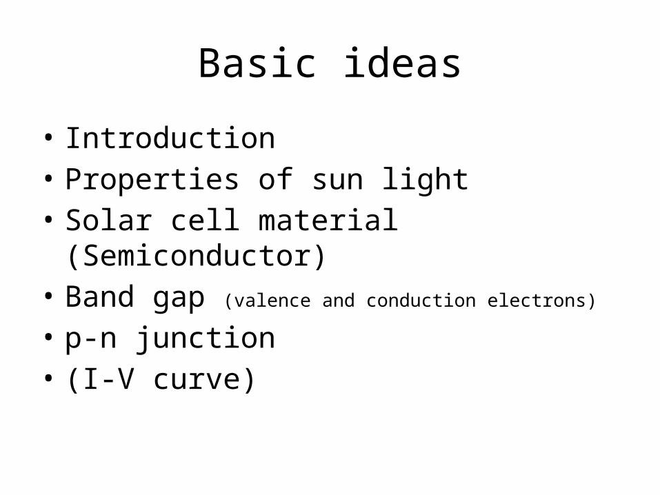
Basic ideas
• Introduction• Properties of sun light• Solar cell material (Semiconductor)• Band gap (valence and conduction electrons) • p-n junction• (I-V curve)

implementation
• Efficiency of different type of solar cells• PV arrays for houses (~ kW range)• Large production arrays (~ MW)

Introduction
• Why would we need solar cells?

Introduction
• Why would we need solar cells?• Local production of power (at small scale)• Need for new energy sources in the future• (end of oil, gas, nuclear)• Need for a ‘clean’ energy source
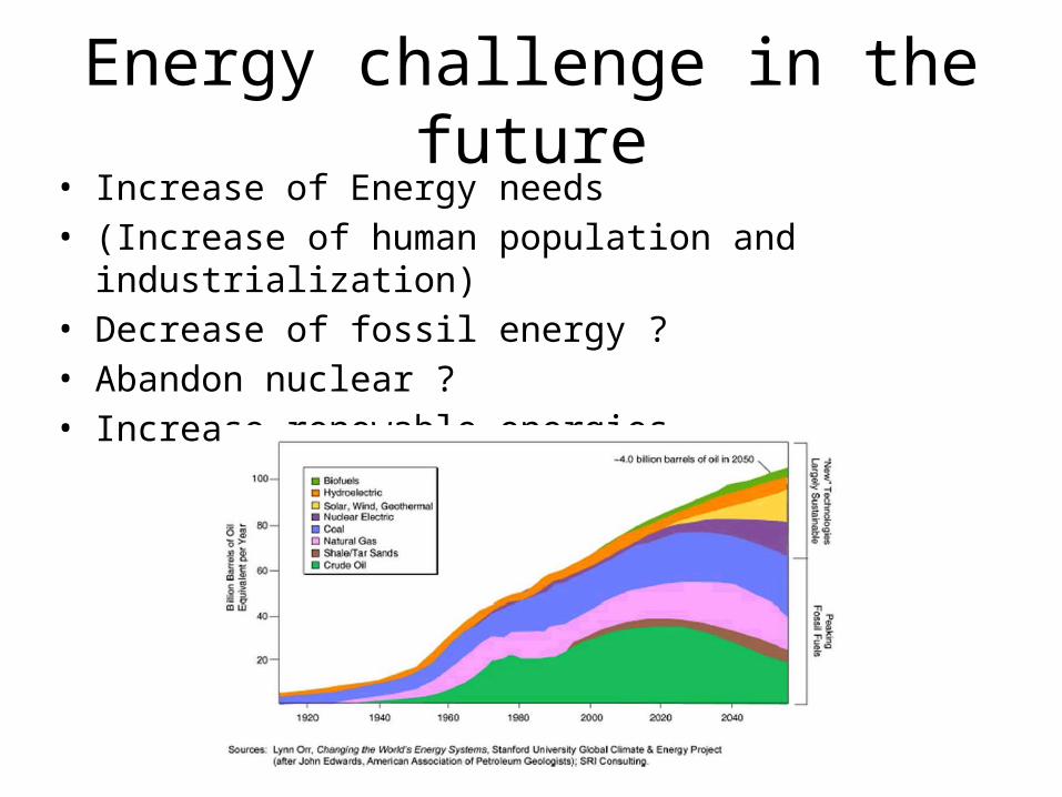
Energy challenge in the future• Increase of Energy needs• (Increase of human population and industrialization)• Decrease of fossil energy ?• Abandon nuclear ?• Increase renewable energies

UN report 2010


Properties of sun light
• Inner part of sun (T ~ 20,000,000 K)• Outer part of sun (T ~ 6000 K)• light coming to earth like black body radiation
at ~6000K. • Missing H and He lines due to absorption in
the sun• Missing absorption from earth’s atmosphere
(O2, H2O, CO2, O3)

http://ocw.mit.edu/courses/mechanical-engineering/2-626-fundamentals-of-photovoltaics-fall-2008/lecture-notes/lecture1.pdf

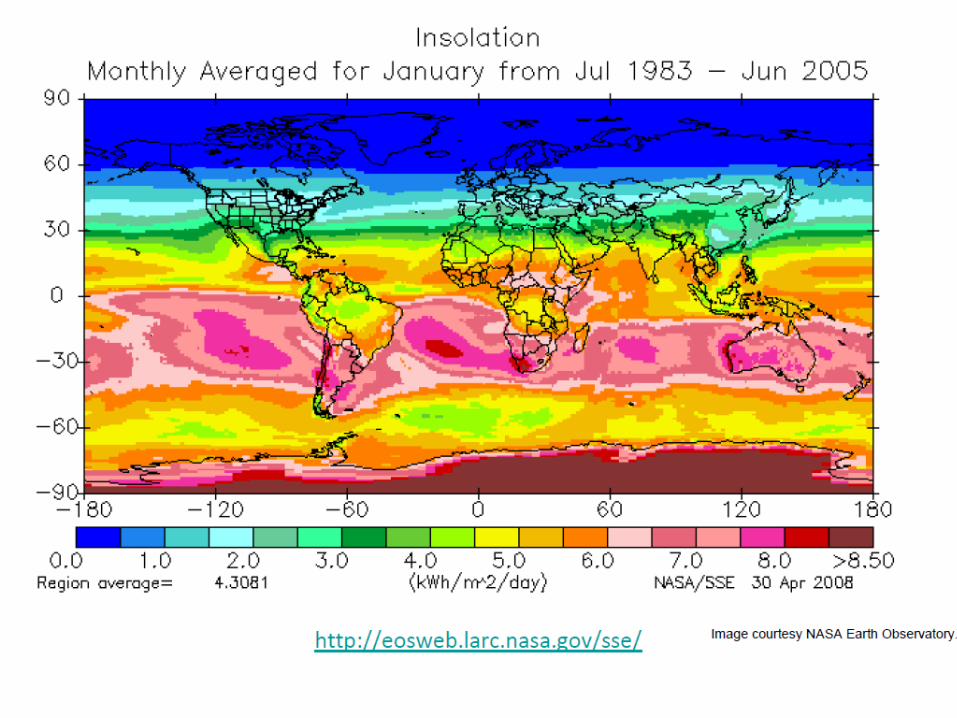


Properties of sun light
• Total power from the sun light hitting the earth: 174,000 TW
• Total human power consumption on earth: ~ 50 TW
(concentration of energy on earth surface:sunlight ~ 200W/m2, wind ~ 2W/m2, geothermal ~ 0.5W/m2)

Classification of solar cells
+ organic materialshttp://sovoxglobal.com/cell_classification.html

Semiconductors (Solar cell material)
• Main technology: Si (~90% of solar cells), mono-crystalline and
poly-crystalline • Thin films: amorphous Si, CaTe, Cu In Ga Se,
GaAs• New technologies : Dye sensitized polymers,
organic materials.• Multi junction cells.

Valence and conduction band
• Valence band: low energy level for electrons (not mobile: insulator) (e- in the crystal bonds)
• Conduction band: high energy level for electrons (mobile: can conduct electricity)
• Semi conductors have (at T=0K) electrons filling the valance band.
• Energy (from temperature, light, etc) can promote valance electrons to the conduction band

Band Gap
http://www2.warwick.ac.uk/fac/sci/eng/staff/pad/teaching/lecture3.pdf
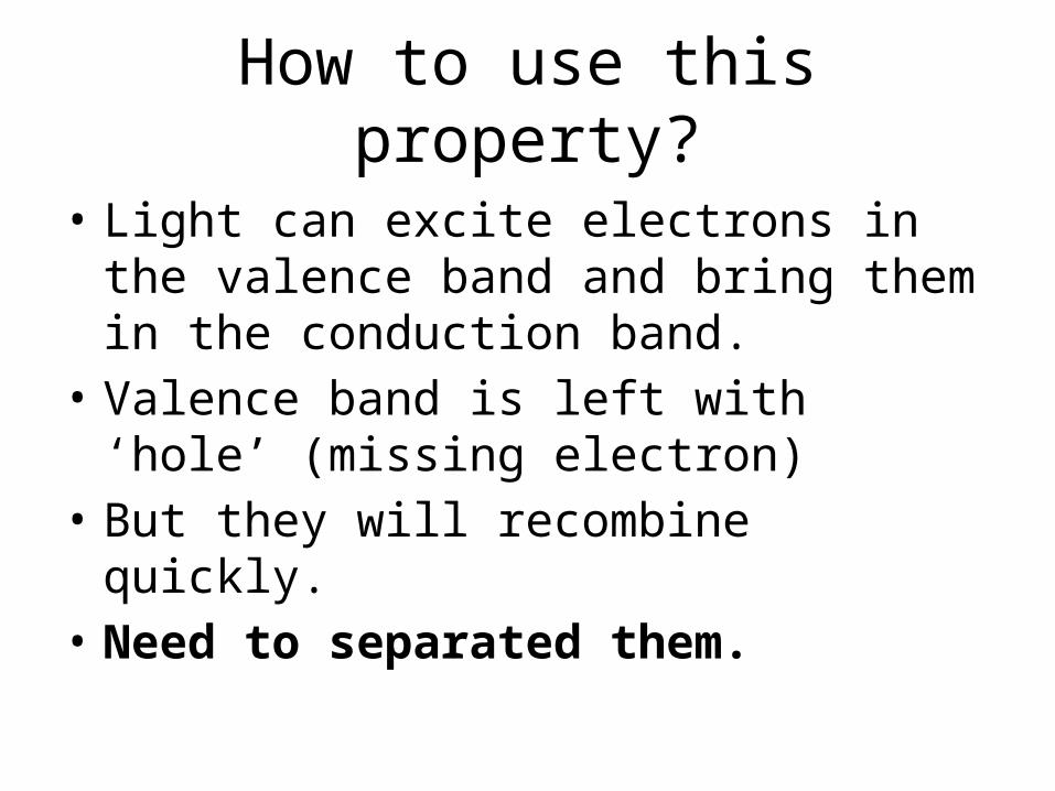
How to use this property?
• Light can excite electrons in the valence band and bring them in the conduction band.
• Valence band is left with ‘hole’ (missing electron)
• But they will recombine quickly.• Need to separated them.

How to use this property?
• Light can excite electrons in the valence band and bring them in the conduction band.
• Valence band is left with ‘hole’ (missing electron)
• But they will recombine quickly.• Need to separated them. -> Create an
electrical field• -> put a battery -> costs energy …
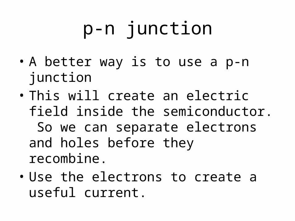
p-n junction
• A better way is to use a p-n junction• This will create an electric field inside the
semiconductor. So we can separate electrons and holes before they recombine.
• Use the electrons to create a useful current.

p-n junction
• Si has 4 valence electron (14 e- in total)
• This 4 electrons are used in the Si-Si-Si-Si crystal bonds.
• B: 3 valence electrons (5 e- total)
• P: 5 valence electrons (15 e- total)
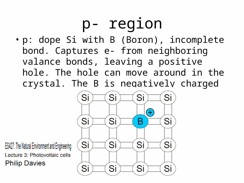
p- region• p: dope Si with B (Boron), incomplete bond.
Captures e- from neighboring valance bonds, leaving a positive hole. The hole can move around in the crystal. The B is negatively charged

n- region • n: dope Si with P (Phophorus), at very low T
the extra electron stays close to the P nucleus. at room T it will move around the crystal. Leaving a positively charged P atom.
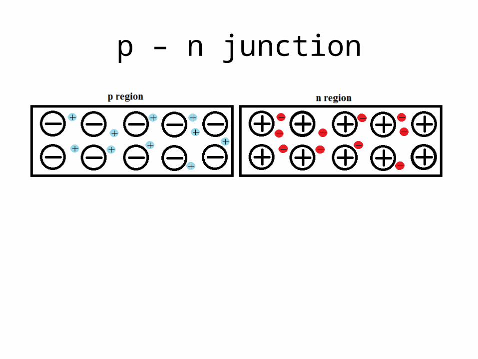
p – n junction

p – n junction

p – n junction

p – n junction
Neutral NeutralCharged Electric field

p-n junction
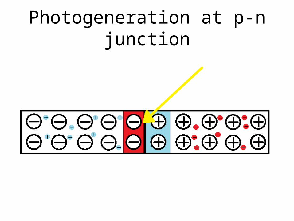
Photogeneration at p-n junction

Photogeneration at p-n junction
Photogeneration at p-n junction
E

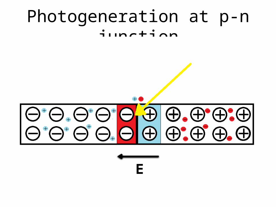
Photogeneration at p-n junction
E

Implications of bandgap
• If photon has E< bandgap : No absorption (photon is lost)
• If photon has E> bandgap: Extra energy is lost in heat.
• Given Sunlight spectrum optimal Bandgap is ~1.4 eV
• Si has 1.1 eV (crystal)
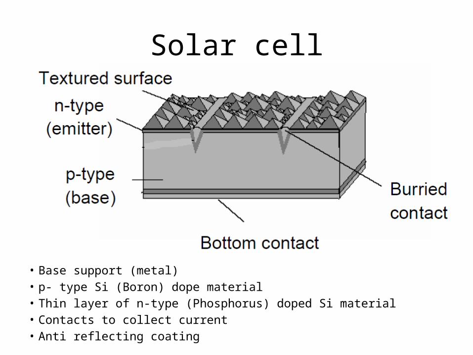
Solar cell
• Base support (metal)• p- type Si (Boron) dope material• Thin layer of n-type (Phosphorus) doped Si material• Contacts to collect current• Anti reflecting coating

Picture of solar cellMono crystal Si poly crystal Si
CdTe
CIGSFlexible
Dye sensitizedTiO2 (semiconductor)
[Ru(4,40-dicarboxy-2,20-bipyridine)2(NCS)2] (N3), Dye photogenerator

Multiple junction solar cellsBest efficiency~ 40%High costUsed in space industry

efficiency
PV arrays
• House arrays in the kW range• Production arrays in the MW range

House arrays in the kW range

PV module
• Mounting angle/ orientation• Electrical circuit DC- AC transformation• Costs
typically 36 connected in series

PV moduleMost PV bulk silicon PV modules consist of• transparent top surface,• encapsulant• rear layer • frame around the outer edge.• In most modules, the top surface is glass, the encapsulant is EVA (ethyl
vinyl acetate) and the rear layer is Tedlar

PV module• A bulk silicon PV module consists of multiple individual solar cells
connected mostly in series
• The voltage of a PV module is usually compatible with a 12V battery.
• An individual silicon solar cell has a voltage of just under 0.6V under 25 °C and AM1.5 illumination.
• 36 solar cells in series give max. 21V (open circuit), operating 18V at max power. Excess voltage is to take care of non optimal conditions.
• Current can be 3.5- 4 A per module, depending on the size of the cells.

Space needs
10ft² = 0.92m²

House array
• 2kW house array• (max possible 2kW x 24h =
48kWh/day)• But sun is not always there
• sunny day (spring South Africa)
• 12kWh/day
• cloudy day• 6 kWh/day
Some ‘typical’ house needs
Fridge 30/150W 2.7kwh(idle / cooling)
TV 80W 500Wh (6h)light 250W 1.8KWh (7h)Heater 3000W 12kWh (7h) pool pump 750W 5.3kWh (7h)Microwave 1200W 600Wh (0.5h)
Total 23kWh (per day)
summer (~20kWh/day)winter (~30kWh/day)

Costs

Production arrays
• Examples : Germany• Examples: Gulf region

Germanyhttp://www.solarbusiness.de/daten-a-fakten/zahlen

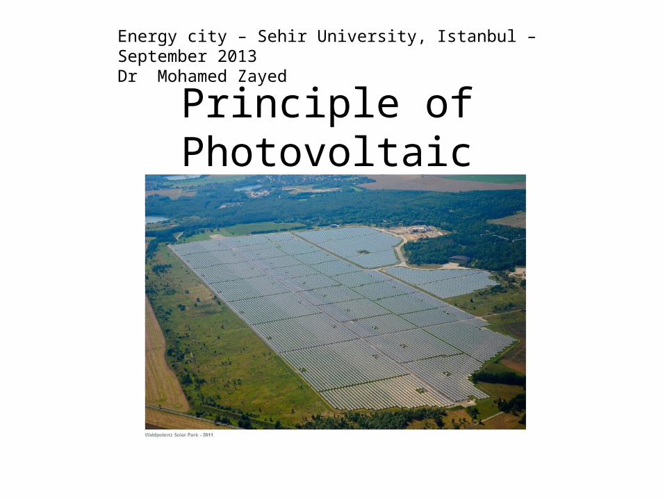
Waldpolenz Solar Park, Germany(thin film technology- CdTe)
Year 200840 MW40,000MWh/year600’000 modules130 M€ investment

Gulf region
• Saudi: plans 41,000MW (16,000 PV) over next 20 years for target 2$/W
• UAE: Shams 1 100MW solar concentration, target 7% of renewable for Abu Dhabi by 2020
• Qatar: 200MW project by 2020+ polysilicon plant at Ras Laffan for PV pannels