principles of embedded system design-seca1706
TRANSCRIPT

1
SCHOOL OF ELECTRICAL AND ELECTRONICS
DEPARTMENT OF ELECTRICAL AND ELECTRONICS ENGINEERING
PRINCIPLES OF EMBEDDED SYSTEM DESIGN-SECA1706

2
UNIT – I
8051 MICROCONTROLLER ARCHITECTURE

3
I. UNIT – I
8051 MICROCONTROLLER ARCHITECTURE
SYLLABUS
Comparison of microprocessors and microcontrollers - 8051 architecture - hardware, I/O
pins, ports, memory, counters, timers, serial I/O interrupts.
Table 1.1-Difference between Microprocessor and microcontroller
Microprocessor Micro Controller
Microprocessor is heart of Computer system. Micro Controller is a heart of embedded system.
It is just a processor. Memory and I/O components have to be connected externally
Micro controller has processor along with internal memory and i/O components
Since memory and I/O has to be connected
externally, the circuit becomes large.
Since memory and I/O are present internally, the
circuit is small.
Cannot be used in compact systems and hence
inefficient
Can be used in compact systems and hence it is
an efficient technique
Cost of the entire system increases Cost of the entire system is low
Due to external components, the entire power
consumption is high. Hence it is not suitable to
used with devices running on stored power like
batteries.
Since external components are low, total power
consumption is less and can be used with devices
running on stored power like batteries.
Most of the microprocessors do not have power
saving features.
Most of the micro controllers have power saving
modes like idle mode and power saving mode.
This helps to reduce power consumption even
further.

4
Since memory and I/O components are all
external, each instruction will need external
operation, hence it is relatively slower.
Since components are internal, most of the
operations are internal instruction, hence speed is
fast.
Microprocessor have less number of registers,
hence more operations are memory based.
Micro controller have more number of registers,
hence the programs are easier to write.
Microprocessors are based on von Neumann
model/architecture where program and data are
stored in same memory module
Micro controllers are based on Harvard
architecture where program memory and Data
memory are separate
Mainly used in personal computers Used mainly in washing machine, MP3 players
5
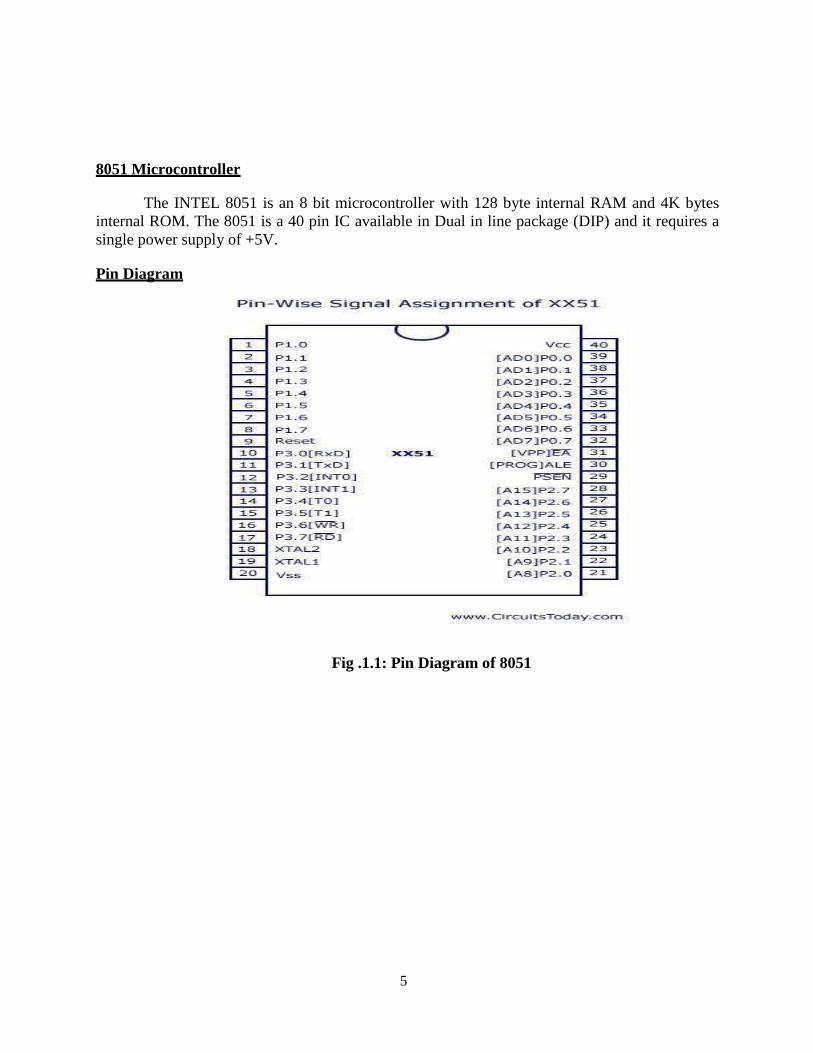
8051 Microcontroller
The INTEL 8051 is an 8 bit microcontroller with 128 byte internal RAM and 4K bytes
internal ROM. The 8051 is a 40 pin IC available in Dual in line package (DIP) and it requires a
single power supply of +5V.
Pin Diagram
Fig .1.1: Pin Diagram of 8051

6
Pin-40 : Named as Vcc is the main power source. Usually its +5V DC.
Pins 32-39: Known as Port 0 (P0.0 to P0.7) – In addition to serving as I/O port, lower order
address and data bus signals are multiplexed with this port (to serve the purpose of external
memory interfacing). This is a bi directional I/O port (the only one in 8051) and external pull up
resistors are required to function this port as I/O.
Pin-31:- ALE aka Address Latch Enable is used to demultiplex the address-data signal of port 0
(for external memory interfacing.) 2 ALE pulses are available for each machine cycle.
Pin-30:- EA/ External Access input is used to enable or disallow external memory interfacing. If
there is no external memory requirement, this pin is pulled high by connecting it to Vcc.
Pin- 29:- PSEN or Program Store Enable is used to read signal from external program memory.
Pins- 21-28:- Known as Port 2 (P 2.0 to P 2.7) – in addition to serving as I/O port, higher order address bus signals are multiplexed with this quasi bi directional port.
Pin 20:- Named as Vss – it represents ground (0 V) connection.
Pins 18 and 19:- Used for interfacing an external crystal to provide system clock.
Pins 10 – 17:- Known as Port 3. This port also serves some other functions like interrupts, timer
input, control signals for external memory interfacing RD and WR , serial communication
signals RxD and TxD etc. This is a quasi bi directional port with internal pull up.
Pin 9:- As explained before RESET pin is used to set the 8051 microcontroller to its initial
values, while the microcontroller is working or at the initial start of application. The RESET pin
must be set high for 2 machine cycles.
Pins 1 – 8:- Known as Port 1. Unlike other ports, this port does not serve any other functions.
Port 1 is an internally pulled up, quasi bi directional I/O port.
8051 Block Diagram (Architecture)
The 8051 architecture consists of the following special features.
8 bit CPU with registers A and B
16 bit Program Counter(PC) and Data Pointer(DPTR)
8 bit Program Status Word(PSW)
8 bit Stack Pointer(SP)
Internal ROM or EPROM of 4K bytes

7
Internal RAM of 128 bytes.
o 4 Register banks , each containing 8 registers
o 16 bytes ,which may be addressed at the bit level
o 80 bytes of general purpose memory
32 input / output pins are arranged as four 8 bit ports : P0-P3
Two 16 bit timer / counters : T0 and T1
Full duplex serial data receiver / transmitter : SBUF
Control registers TCON,TMOD,SCON,PCON,IP and IE
2 external and 3 internal interrupt sources
Oscillator and Clock circuits.
8051 System Clock
Fig 1.2: Architecture of 8051
Fig 1.3: 8051 System clock

8
An 8051 clock circuit is shown above. In general cases, a quartz crystal is used to make the clock
circuit. The connection is shown in figure and note the connections to XTAL 1 and XTAL 2. In
some cases external clock sources are used and you can see the various connections above. Clock
frequency limits (maximum and minimum) may change from device to device. Standard practice
is to use 12MHz frequency. If serial communications are involved then its best to use 11.0592
MHz frequency.
Fig 1.4: Clock signal of 8051
Okay, take a look at the above machine cycle waveform. One complete oscillation of the clock
source is called a pulse. Two pulses forms a state and six states forms one machine cycle. Also
note that, two pulses of ALE are available for 1 machine cycle.
ALU
All arithmetic and logical functions are carried out by the ALU.
Addition, subtraction with carry, and multiplication come under arithmetic operations.
Logical AND, OR and exclusive OR (XOR) come under logical operations.
Registers
Registers are usually known as data storage devices.

9
A & B Registers
8051 microcontroller has 2 registers, namely Register A and Register B. Register A serves as an
accumulator while Register B functions as a general purpose register. These registers are used to
store the output of mathematical and logical instructions.
The operations of addition, subtraction, multiplication and division are carried out by Register A.
Register B is usually unused and comes into picture only when multiplication and division
functions are carried out by Register A. Register A also involved in data transfers between the
microcontroller and external memory.
Program Counter (PC)
A program counter is a 16-bit register and it has no internal address. The basic function of
program counter is to fetch from memory the address of the next instruction to be executed. The
PC holds the address of the next instruction residing in memory and when a command is
encountered, it produces that instruction. This way the PC increments automatically, holding the
address of the next instruction.
Data Pointer (DPTR)
The data pointer or DPTR is a 16-bit register. It is made up of two 8-bit registers called DPH and
DPL. Separate addresses are assigned to each of DPH and DPL. These 8-bit registers are used for
the storing the memory addresses that can be used to access internal and external data/code.
Stack Pointer (SP)
The stack pointer (SP) in 8051 is an 8-bit register. The main purpose of SP is to access the stack.
As it has 8-bits it can take values in the range 00 H to FF H. Stack is a special area of data in memory. The SP acts as a pointer for an address that points to the top of the stack.
PSW (Program Status Word)
Program Status Word or PSW is a hardware register which is a memory location which holds a
program's information and also monitors the status of the program this is currently being
executed. PSW also has a pointer which points towards the address of the next instruction to be
executed. PSW register has 3 fields namely are instruction address field, condition code field and
error status field. We can say that PSW is an internal register that keeps track of the computer at
every instant.Generally, the instruction of the result of a program is stored in a single bit register
called a 'flag'. The are7 flags in the PSW of 8051. Among these 7 flags, 4 are math flags and 3
are general purpose user flags.

10
\
The 4 Math flags are: Carry flag(C), Auxiliary Carry (AC) ,Overflow (OV) and Parity (P)
The 3 General purpose flags or User flags are: FO, GFO and GF 1
CY PSW.7 Carry flag (Carry out from the D7 bit)
AC PSW.6 Auxiliary carry flag (A carry from D3 to D4)
— PSW.5 Available to the user for general purpose
RS1 PSW.4 Register Bank selector bit 1.
RS0 PSW.3 Register Bank selector bit 0.
OV PSW.2 Overflow flag.
— PSW.1 User definable bit.
P PSW.0 Parity flag. Set/cleared by hardware each instruction cycle to indicate an
odd/ even number of 1 bits in the accumulator.
Special function registers
The table1.2 shows the list of special function registers for various operations in 8051.

11
Table 1.2- Special Function Registers
Internal RAM and ROM
ROM
A code of 4K memory is incorporated as on-chip ROM in 8051. The 8051 ROM is a non-volatile
memory meaning that its contents cannot be altered and hence has a similar range of data and
program memory, i.e, they can address program memory as well as a 64K separate block of data
memory.

12
RAM
The 8051 microcontroller is composed of 128 bytes of internal RAM. This is a volatile memory
since its contents will be lost if power is switched off. These 128 bytes of internal RAM are
divided into 32 working registers which in turn constitute 4 register banks (Bank 0-Bank 3) with
each bank consisting of 8 registers (R0 - R7). There are 128 addressable bits in the internal
RAM.
Fig 1.5: Register Bank
Data and Address Bus
A bus is group of wires using which data transfer takes place from one location to another within
a system. Buses reduce the number of paths or cables needed to set up connection between
components. There are mainly two kinds of buses - Data Bus and
Address Bus
Data Bus: The purpose of data bus is to transfer data. It acts as an electronic channel using
which data travels. Wider the width of the bus, greater will be the transmission of data.
Address Bus: The purpose of address bus is to transfer information but not data. The
information tells from where within the components, the data should be sent to or
received from. The capacity or memory of the address bus depends on the number of wires that
transmit a single address bit.

13
Four General Purpose Parallel Input/Output Ports
The 8051 microcontroller has four 8-bit input/output ports. These are:
PORT P0: When there is no external memory present, this port acts as a general purpose
input/output port. In the presence of external memory, it functions as a multiplexed address and
data bus. It performs a dual role.
PORT P1: This port is used for various interfacing activities. This 8-bit port is a normal I/O port
i.e. it does not perform dual functions.
PORT P2: Similar to PORT P0, this port can be used as a general purpose port when there is no
external memory but when external memory is present it works in conjunction with PORT PO as
an address bus. This is an 8-bit port and performs dual functions.
PORT P3: PORT P3 behaves as a dedicated I/O port
PORT 0 :
The structure of a Port-0 pin is shown in fig 6.It has 8 pins (P0.0-P0.7).
Fig 1.6: PORT 0 STRUCTURE
Port-0 can be used as a normal bidirectional I/O port or it can be used for address/data
interfacing for accessing external memory. When control is '1', the port is used for address/data
interfacing. When the control is '0', the port can be used as a bidirectional I/O port.
PORT 0 as an Input Port
Let us assume that control is '0'. When the port is used as an input port, '1' is written to the latch.
In this situation both the output MOSFETs are 'off'. Hence the output pin have floats hence
whatever data written on pin is directly read by read pin.

14
Fig 1.7: PORT 0-INPUT PORT
PORT 0 as an Output Port
Suppose we want to write 1 on pin of Port 0, a '1' written to the latch which turns 'off' the lower
FET while due to '0' control signal upper FET also turns off as shown in fig. above. Here we
wants logic '1' on pin but we getting floating value so to convert that floating value into logic '1'
we need to connect the pull up resistor parallel to upper FET . This is the reason why we needed
to connect pull up resistor to port 0 when we want to initialize port 0 as an output port.
Fig 1.8: PORT 0 PULL-UP RESISTORS

15
If we want to write '0' on pin of port 0 , when '0' is written to the latch, the pin is pulled down
by the lower FET. Hence the output becomes zero.
Fig 1.9: PORT 0 –OUTPUT PORT
When the control is '1', address/data bus controls the output driver FETs. If the address/data bus
(internal) is '0', the upper FET is 'off' and the lower FET is 'on'. The output becomes '0'. If the
address/data bus is '1', the upper FET is 'on' and the lower FET is 'off'. Hence the output is '1'.
Hence for normal address/data interfacing (for external memory access) no pull-up resistors are
required.Port-0 latch is written to with 1's when used for external memory access.
PORT 1:
The structure of a port-1 pin is shown in fig below.It has 8 pins (P1.1-P1.7) .
Port-1 dedicated only for I/O interfacing. When used as output port, not needed to connect
additional pull-up resistor like port 0. It have provided internally pull-up resistor as shown in fig.
below. The pin is pulled up or down through internal pull-up when we want to initialize as an
output port. To use port-1 as input port, '1' has to be written to the latch. In this input mode when
'1' is written to the pin by the external device then it read fine. But when '0' is written to the pin
by the external device then the external source must sink current due to internal pull-up. If the
external device is not able to sink the current the pin voltage may rise, leading to a possible
wrong reading.

16
Fig 1.10: PORT 1
PORT 2:
The structure of a port-2 pin is shown in fig. below. It has 8-pins (P2.0-P2.7) .
Fig 1.11: PORT 2

17
Port-2 we use for higher external address byte or a normal input/output port. The I/O operation is
similar to Port-1. Port-2 latch remains stable when Port-2 pin are used for external memory
access. Here again due to internal pull-up there is limited current driving capability.
PORT 3:
Port-3 (P3.0-P3.7) having alternate functions to each pin,The internal structure of a port-3 pin is
shown in fig below.
Fig 1.12: PORT 3
Following are the alternate functions of port 3:
TABLE 1.3: Alternate Functions of Port 3
It work as an IO port same like Port 2. only alternate function of port 3 makes its architecture
different than other ports.
18
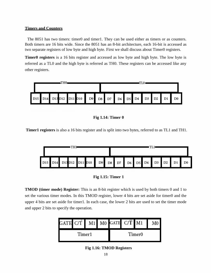
Timers and Counters
The 8051 has two timers: timer0 and timer1. They can be used either as timers or as counters.
Both timers are 16 bits wide. Since the 8051 has an 8-bit architecture, each 16-bit is accessed as
two separate registers of low byte and high byte. First we shall discuss about Timer0 registers.
Timer0 registers is a 16 bits register and accessed as low byte and high byte. The low byte is
referred as a TL0 and the high byte is referred as TH0. These registers can be accessed like any
other registers.
Fig 1.14: Timer 0
Timer1 registers is also a 16 bits register and is split into two bytes, referred to as TL1 and TH1.
Fig 1.15: Timer 1
TMOD (timer mode) Register: This is an 8-bit register which is used by both timers 0 and 1 to
set the various timer modes. In this TMOD register, lower 4 bits are set aside for timer0 and the
upper 4 bits are set aside for timer1. In each case, the lower 2 bits are used to set the timer mode
and upper 2 bits to specify the operation.
Fig 1.16: TMOD Registers

19
TMOD
In upper or lower 4 bits, first bit is a GATE bit. Every timer has a means of starting and stopping.
Some timers do this by software, some by hardware, and some have both software and hardware
controls. The hardware way of starting and stopping the timer by an external source is achieved
by making GATE=1 in the TMOD register. And if we change to GATE=0 then we do no need
external hardware to start and stop the timers. The second bit is C/T bit and is used to decide
whether a timer is used as a time delay generator or an event counter. If this bit is 0 then it is
used as a timer and if it is 1 then it is used as a counter. In upper or lower 4 bits, the last bits third
and fourth are known as M1 and M0 respectively. These are used to select the timer mode.
M0 M1 Mode Operating Mode
0 0 0 13-bit timer mode, 8-bit timer/counter THx and TLx as 5-bit prescalar.
0 1 1 16-bit timer mode, 16-bit timer/counters THx and TLx are cascaded;
There are no prescalar.
1 0 2 8-bit auto reload mode, 8-bit auto reload timer/counter; THx holds a
value which is to be reloaded into TLx eachtime it overflows.
1 1 3 Spilt timer mode.
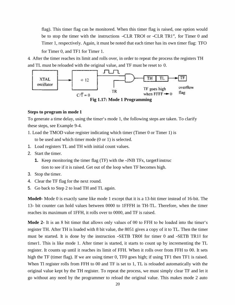
Mode 1- It is a 16-bit timer; therefore it allows values from 0000 to FFFFH to be loaded into the
timer‗s registers TL and TH. After TH and TL are loaded with a 16-bit initial value, the timer
must be started. We can do it by ―SETB TR0‖ for timer 0 and ―SETB TR1‖ for timer 1. After the
timer is started. It starts count up until it reaches its limit of FFFFH. When it rolls over from
FFFF to 0000H, it sets high a flag bit called TF (timer flag). This timer flag can be monitored.
When this timer flag is raised, one option would be stop the timer with the instructions ―CLR
TR0― or CLR TR1 for timer 0 and timer 1 respectively. Again, it must be noted that each timer
flag TF0 for timer 0 and TF1 for timer1. After the timer reaches its limit and rolls over, in order
to repeat the process the registers TH and TL must be reloaded with the original value and TF
must be reset to 0.
Mode 1 programming
The following are the characteristics and operations of mode 1:
1. It is a 16-bit timer; therefore, it allows values of 0000 to FFFFH to be loaded into
the timer‗s registers TL and TH.
2. After TH and TL are loaded with a 16-bit initial value, the timer must be start ed.
This is done by ―SETB TRO‖ for Timer 0 and ―SETB TR1″ for Timer 1.
3. After the timer is started, it starts to count up. It counts up until it reaches its limit of
FFFFH. When it rolls over from FFFFH to 0000, it sets high a flag bit called TF (timer
20
flag). This timer flag can be monitored. When this timer flag is raised, one option would
be to stop the timer with the instructions ―CLR TRO‖ or ―CLR TR1″, for Timer 0 and
Timer 1, respectively. Again, it must be noted that each timer has its own timer flag: TFO
for Timer 0, and TF1 for Timer 1.
4. After the timer reaches its limit and rolls over, in order to repeat the process the registers TH
and TL must be reloaded with the original value, and TF must be reset to 0.
Fig 1.17: Mode 1 Programming
Steps to program in mode 1
To generate a time delay, using the timer‗s mode 1, the following steps are taken. To clarify
these steps, see Example 9-4.
1. Load the TMOD value register indicating which timer (Timer 0 or Timer 1) is
to be used and which timer mode (0 or 1) is selected.
1. Load registers TL and TH with initial count values.
2. Start the timer.
1. Keep monitoring the timer flag (TF) with the ―JNB TFx, target‖ instruc
tion to see if it is raised. Get out of the loop when TF becomes high.
3. Stop the timer.
4. Clear the TF flag for the next round.
5. Go back to Step 2 to load TH and TL again.
Mode0- Mode 0 is exactly same like mode 1 except that it is a 13-bit timer instead of 16-bit. The
13- bit counter can hold values between 0000 to 1FFFH in TH-TL. Therefore, when the timer
reaches its maximum of 1FFH, it rolls over to 0000, and TF is raised.
Mode 2- It is an 8 bit timer that allows only values of 00 to FFH to be loaded into the timer‗s
register TH. After TH is loaded with 8 bit value, the 8051 gives a copy of it to TL. Then the timer
must be started. It is done by the instruction ―SETB TR0‖ for timer 0 and ―SETB TR1‖ for
timer1. This is like mode 1. After timer is started, it starts to count up by incrementing the TL
register. It counts up until it reaches its limit of FFH. When it rolls over from FFH to 00. It sets
high the TF (timer flag). If we are using timer 0, TF0 goes high; if using TF1 then TF1 is raised.
When Tl register rolls from FFH to 00 and TF is set to 1, TL is reloaded automatically with the
original value kept by the TH register. To repeat the process, we must simply clear TF and let it
go without any need by the programmer to reload the original value. This makes mode 2 auto

21
reload, in contrast in mode 1 in which programmer has to reload TH and TL.
1. Mode 2 programming
The following are the characteristics and operations of mode 2.
1. It is an 8-bit timer; therefore, it allows only values of 00 to FFH to be
loaded
into the timer‗s register TH.
2. After TH is loaded with the 8-bit value, the 8051 gives a copy of it to TL.
Then
the timer must be started. This is done by the instruction ―SETB TRO‖ for
Timer 0 and ―SETB TR11‗ for Timer 1. This is just like mode 1.
3. After the timer is started, it starts to count up by incrementing the TL
register.
It counts up until it reaches its limit of FFH. When it rolls over from FFH to
00, it sets high the TF (timer flag). If we are using Timer 0, TFO goes high;
if
we are using Timer 1, TF1 is raised.
Fig 1.18 Mode 1 Programming
4. When the TL register rolls from FFH to 0 and TF is set to 1, TL is reloaded
automatically with the original value kept by the TH register. To repeat the process, we
must simply clear TF and let it go without any need by the programmer to reload the
original value. This makes mode 2 an auto-reload, in contrast with mode 1 in which the
programmer has to reload TH and TL.
It must be emphasized that mode 2 is an 8-bit timer. However, it has an auto- reloading
capability. In auto-reload, TH is loaded with the initial count and a copy of it is given to TL.
This reloading leaves TH unchanged, still holding a copy of the original value. This mode
has many applications, including setting the baud rate in serial communication, as we will see
in Chapter 10.
Steps to program in mode 2
To generate a time delay using the timer‗s mode 2, take the following steps.
22
1Load the TMOD value register indicating which timer (Timer 0 or Timer 1) is to be
used, and select the timer mode (mode 2).
2. Load the TH registers with the initial count value.
3. Start the timer.
3. Keep monitoring the timer flag (TF) with the ―JNB TFx, target‖ instruc tion
to see whether it is raised. Get out of the loop when TF goes high.
4. Clear the TF flag.
5. Go back to Step 3, since mode 2 is auto-reload.
Mode3- Mode 3 is also known as a split timer mode. Timer 0 and 1 may be programmed to be in
mode 0, 1 and 2 independently of similar mode for other timer. This is not true for mode 3;
timers do not operate independently if mode 3 is chosen for timer 0. Placing timer 1 in mode 3
causes it to stop counting; the control bit TR1 and the timer 1 flag TF1 are then used by timer0.
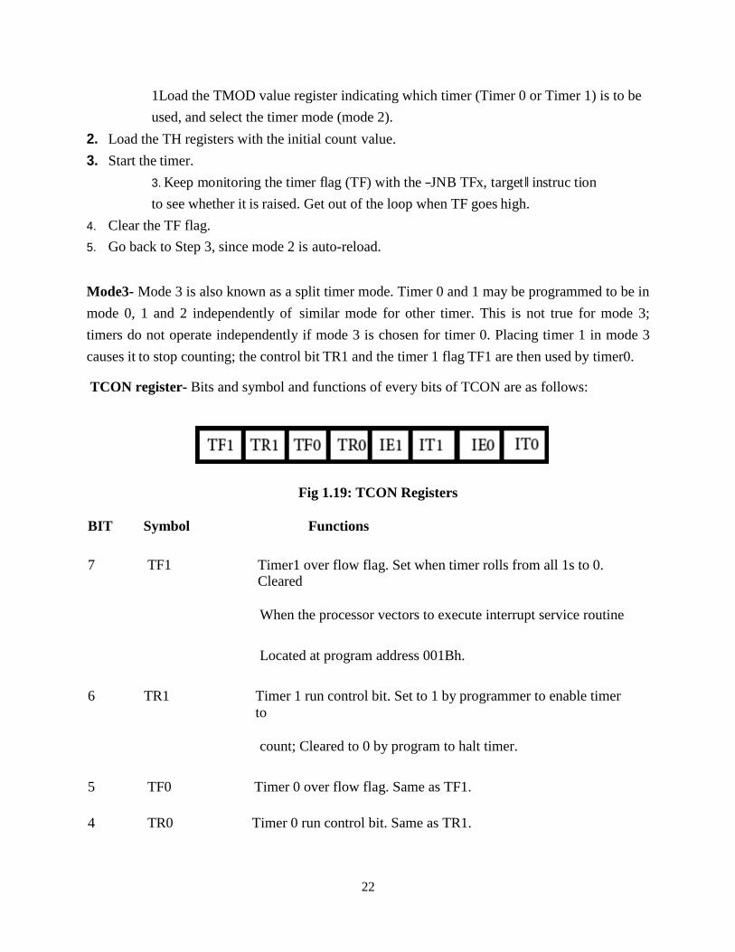
TCON register- Bits and symbol and functions of every bits of TCON are as follows:
Fig 1.19: TCON Registers
BIT Symbol Functions
7 TF1 Timer1 over flow flag. Set when timer rolls from all 1s to 0. Cleared
When the processor vectors to execute interrupt service routine
Located at program address 001Bh.
6 TR1 Timer 1 run control bit. Set to 1 by programmer to enable timer
to
count; Cleared to 0 by program to halt timer.
5 TF0 Timer 0 over flow flag. Same as TF1.
4 TR0 Timer 0 run control bit. Same as TR1.

23
3 IE1 External interrupt 1 Edge flag. Not related to timer operations.
2 IT1 External interrupt1 signal type control bit. Set to 1 by program to
Enable external interrupt 1 to be triggered by a falling edge signal. Set
To 0 by program to enable a low level signal on external interrupt1 to
generate an interrupt.
1 IE0 External interrupt 0 Edge flag. Not related to timer operations.
0 IT0 External interrupt 0 signal type control bit. Same as IT0.
Interrupt Control
An event which is used to suspend or halt the normal program execution for a temporary period
of time in order to serve the request of another program or hardware device is called an interrupt.
An interrupt can either be an internal or external event which suspends the microcontroller for a
while and thereby obstructs the sequential flow of a program.
There are two ways of giving interrupts to a microcontroller – one is by sending software
instructions and the other is by sending hardware signals. The interrupt mechanism keeps the
normal program execution in a "put on hold" mode and executes a subroutine program and after
the subroutine is executed, it gets back to its normal program execution. This subroutine program
is also called an interrupt handler. A subroutine is executed when a certain event occurs.
These five sources of interrupts in 8051are: ( 1,2 and 5 are internal interrupts . 3 and 4 are
external interrupts).
1. Timer 0 overflow interrupt- TF0
2. Timer 1 overflow interrupt- TF1
3. External hardware interrupt- INT0
4. External hardware interrupt- INT1
5. Serial communication interrupt- RI/TI

24
The Timer and Serial interrupts are internally generated by the microcontroller, whereas the
external interrupts are generated by additional interfacing devices or switches that are externally
connected to the microcontroller. These external interrupts can be edge triggered or level
triggered. When an interrupt occurs, the microcontroller executes the interrupt service routine
so that memory location corresponds to the interrupt that enables it. The Interrupt corresponding
to the memory location is given in the interrupt vector table below.
TABLE 1.4: Interrupt Vector Table
Interrupt Source
Vector address
Interrupt
priority
External Interrupt 0 –INT0
0003H
1
Timer 0 Interrupt
000BH
2
External Interrupt 1 –INT1
0013H
3
Timer 1 Interrupt
001BH
4
Serial Interrupt
0023H
5
Interrupt Enable register
This register is responsible for enabling and disabling the interrupt. It is a bit addressable register
in which EA must be set to one for enabling interrupts. The corresponding bit in this register
enables particular interrupt like timer, external and serial inputs. In the below IE register, bit
corresponding to 1 activates the interrupt and 0 disables the interrupt.
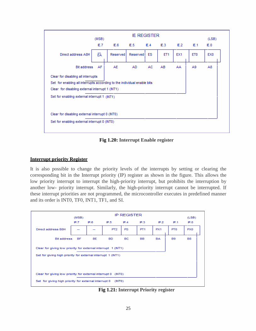
25
Fig 1.20: Interrupt Enable register
Interrupt priority Register
It is also possible to change the priority levels of the interrupts by setting or clearing the
corresponding bit in the Interrupt priority (IP) register as shown in the figure. This allows the
low priority interrupt to interrupt the high-priority interrupt, but prohibits the interruption by
another low- priority interrupt. Similarly, the high-priority interrupt cannot be interrupted. If
these interrupt priorities are not programmed, the microcontroller executes in predefined manner
and its order is INT0, TF0, INT1, TF1, and SI.
Fig 1.21: Interrupt Priority register

26
Serial Data Communication
A method of establishing communication among computers is by transmitting and receiving data
bits is a serial connection network. In 8051, the SBUF (Serial Port Data Buffer) register holds the
data; the SCON (Serial Control) register manages the data communication and the PCON (Power
Control) register manages the data transfer rates. Further, two pins - RXD and TXD, establish the
serial network.
The SBUF register has 2 parts – one for storing the data to be transmitted and another for
receiving data from outer sources. The first function is done using TXD pin and the second
function is done using RXD pin.
SCON Register
There are 4 programmable modes in serial data communication. They are:
1. Serial Data mode 0 (shift register mode) 2. Serial Data mode 1 (standard UART)
3. Serial Data mode 2 (multiprocessor mode)
4. Serial Data mode 3
TABLE 1.5: Programmable Modes in Serial Data Communication
SM0 SM1 Mode/Description/Baud rate
0 0 0,shift register,(Fosc./12)
0 1 1,8 bit UART,Variable
1 0 2,9 bit UART,(Fosc./64) OR (Fosc./32)
1 1 3,9 bit UART, Variable
SMO, SM1
SMO and SMI are D7 and D6 of the SCON register, respectively. These two bits determine the
framing of data by specifying the number of bits per character, and the start and stop bits. They
take the following combinations.

27
Of the 4 serial modes, only mode I is of interest to us. Further explanation for the other three
modes is in Appendix A.2. They are rarely used today. In the SCON register, when serial mode 1
is chosen, the data framing is 8 bits, 1 stop bit, and 1 start bit, which makes it compatible with
the COM port of IBM/compatible PCs. More importantly, serial mode 1 allows the baud rate to
be variable and is set by Timer 1 of the 8051. In serial mode 1, for each character a total of 10
bits are transferred, where the first bit is the start bit, followed by 8 bits of data, and finally 1 stop
bit.
SM2
SM2 is the D5 bit of the SCON register. This bit enables the multiprocessing capability of the
8051 and is beyond the discussion of this chapter. For our applications, we will make SM2 = 0
since we are not using the 8051 in a multiprocessor environment.
REN
The REN (receive enable), bit is D4 of the SCON register. The REN bit is also referred to as
SCON.4 since SCON is a bit-addressable register. When the REN bit is high, it allows the 8051
to receive data on the RxD pin of the 8051. As a result if we want the 8051 to both transfer and
receive data, REN must be set to 1. By making REN = 0, the receiver is disabled. Making REN
— 1 or REN = 0 can be achieved by the instructions ―SETB SCON. 4″ and ―CLR SCON. 4″,
respectively. Notice that these instructions use the bit-addressable features of register SCON.
This bit can be used to block any serial data reception and is an extremely important bit in the
SCON register.
TBS
TBS (transfer bit 8) is bit D3 of SCON. It is used for serial modes 2 and 3. We make TBS = 0
since it is not used in our applications.
RB8
RB8 (receive bit 8) is bit D2 of the SCON register. In serial mode 1, this bit gets a copy of the
stop bit when an 8-bit data is received. This bit (as is the case for TBS) is rarely used anymore.
In all our applications we will make RB8 = 0. Like TB8, the RB8 bit is also used in serial modes
2 and 3.
Tl

28
TI (transmit interrupt) is bit Dl of the SCON register. This is an extremely important flag bit in
the SCON register. When the 8051 finishes the transfer of the 8-bit character, it raises the TI flag
to indicate that it is ready to transfer another byte. The TI bit is raised at the beginning of the stop
bit. We will discuss its role further when programming examples of data transmission are given.
Rl
RI (receive interrupt) is the DO bit of the SCON register. This is another extremely important
flag bit in the SCON register. When the 8051 receives data serially via RxD, it gets rid of the
start and stop bits and places the byte in the SBUF register. Then it raises the RI flag bit to
indicate that a byte has been received and should be picked up before it is lost. RI is raised
halfway through the stop bit, and we will soon see how this bit is used in programs for receiving
data serially.
Programming the 8051 to transfer data serially
In programming the 8051 to transfer character bytes serially, the following steps must be taken.
1. The TMOD register is loaded with the value 20H, indicating the use ofTimer 1 in
mode 2 (8-bit auto-reload) to set the baud rate.
2. The TH1 is loaded with one of the values in Table 10-4 to set the baud ratefor serial
data transfer (assuming XTAL = 11.0592 MHz).
3. The SCON register is loaded with the value 50H, indicating serial mode 1, where
an 8-bit data is framed with start and stop bits.
1. TR1 is set to 1 to start Timer 1.
2. TI is cleared by the ―CLR TI‖ instruction.
3. The character byte to be transferred serially is written into the SBUF register.
1. The TI flag bit is monitored with the use of the instruction ‖ JNB TI, xx‖ to see
if the character has been transferred completely.
4. To transfer the next character, go to Step 5.
5. Programming the 8051 to receive data serially
In the programming of the 8051 to receive character bytes serially, the following steps
must be taken.
1. The TMOD register is loaded with the value 20H, indicating the use of
Timer
1 in mode 2 (8-bit auto-reload) to set the baud rate.
2. TH1 is loaded with one of the values in Table 10-4 to set the baud rate
(assum
ing XTAL = 11.0592MHz).

29
3. The SCON register is loaded with the value 50H, indicating serial mode 1, where
8-bit data is framed with start and stop bits and receive enable is turned
on.
6. TR1 is set to 1 to start Timer 1.
7. RI is cleared with the ―CLR RI‖ instruction.
1. The RI flag bit is monitored with the use of the instruction ―JNB RI, xx‖ to see
if an entire character has been received yet.
8. When RI is raised, SBUF has the byte. Its contents are moved into a safe place.
9. To receive the next character, go to Step 5.
External memory interface with 8051
Address/Data Multiplexing
From Figure, it is important to note that normally ALE = 0, and PO is used as a data bus,
sending data out or bringing data in. Whenever the 8031/51 wants to use PO asan address bus, it
puts the addresses AO – A7 on the PO pins and activates ALE = 1 to indicate that PO has the
addresses.
PSEN
Another important signal for the 8031/51 is the PSEN (program store enable) signal. PSEN is an
output signal for the 8031/51 microcontroller and must be connected to the OE pin of a ROM
containing the program code. In other words, to access external ROM containing program code,
the 8031/51 uses the PSEN signal. It is important to emphasize the role of EA and PSEN when
connecting the 8031/51 to external ROM. When the EA pin is connected to GND, the 8031/51
fetches opcode from external ROM by using PSEN. The connection of the PSEN pin to the OE
pin of ROM. In systems based on the 8751/89C51/DS5000 where EA is connected to VCC,
these chips do not activate the PSEN pin. This indicates that the on-chip ROM contains program
code.
In systems where the external ROM contains the program code, burning the program into ROM
leaves the microcontroller chip untouched. This is preferable in some applications due to
flexibility. In such applications the software is updated via the serial or parallel ports of the IBM
PC. This is especially the case during software development and this method is widely used in
many 8051-based trainers and emulators.

30
Fig 1.22: External memory interface with 8051
TEXT / REFERENCE BOOKS
1. Kenneth. J. Ayala, ―The 8051 Microcontroller Architecture, Programming and Apllications‖, Penram
International, 1996, 2 nd Edition.
2. Sriram. V. Iyer, Pankaj Gupta, ―Embedded Real Time Systems Programming‖, 2004 Tata McGraw Hill
Publishing Company Limited, 2006.
3. Frank Vahid, Tony Givargis, ‗Embedded system Design - A unified Hardware / software Introduction‘,
John Wiley and Sons, 2002.
4. Todd D Morton, ‗Embedded Microcontrollers‘, Reprint by 2005, Low Price Edition. 5. Muhammed Ali Mazidi, Janice Gillispie Mazidi, ‗The 8051 Microcontroller and Embedded Systems‘,
Low Price Edition, Second Impression 2006.
6. Raj Kamal, ‗Embedded Systems-Architecture, Programming and Design‘, Tata McGraw Hill
Publishing Company Limited 2003.
7. Muhammed Ali Mazidi, Rolin D.Mckinlay, Dannycauscy, ―PIC microcontrollers and embedded
systems using assembly and C‖, 1st edition, Pearson, 2007.

1
SCHOOL OF ELECTRICAL AND ELECTRONICS
DEPARTMENT OF ELECTRICAL AND ELECTRONICS ENGINEERING
PRINCIPLES OF EMBEDDED SYSTEM DESIGN-SECA1706

2
UNIT – II
PROGRAMMING OF 8051

3
II. UNIT – II
Programming of 8051
SYLLABUS
Addressing modes - Instruction sets - Simple programs with 8051 -I/O
Programming.- Timer programming-Serial communication programs - Delay
Programs.
Addressing Modes
Data or value can be specified in the instruction itself or it can be stored in the
registers, internal memory and external memory
Definition
The method of specifying the data to be operated by the instruction is called
addressing Mode.
Fig 2.1: Addressing Modes of 8051
1. Immediate Addressing Mode
This method is the simplest method to get the data.
An 8/16 bit immediate data / constant is specified in the instruction itself.
The immediate data must be preceded by ―#‖ sign
Examples
MOV R3, #45H - Data 45H is copied into R3

4
Register
MOV A, #0AFH - Data AFH is copied into A
Register
MOV DPTR, #4500H - Data 4500H is copied into
DPTR Register
2. Register Addressing Mode
Register addressing mode involves the use of registers to hold the data to be
manipulated
Permits access to eight registers(R0-R7) of register bank
Examples
MOV A, R5 ; Data available in R5 is copied to A
MOV R0, A ; Data available in A is copied to R0
ADD A,R5; Add the content of R5 to content of A
3. Direct Addressing Mode
Address of the data is directly specified in the instruction.
The direct address can be the address of an internal data RAM location (00H to
7FH) or address of special function register (80H to FFH).
Examples MOV R2, 45H ; Data stored in the location 45H is
copied to R2 Register
MOV R0, 05H; Data stored in the location 05H is
copied to R2 Register
4. Register Indirect Addressing Mode
Instruction specifies the name of the register in which the address of the data is
available.
Source or destination address is given in the register.
A register is used as a pointer to the data
R0 and R1 are used for 8-bit addresses, and DPTR is used for 16-bit addresses, no
other registers can be used for addressing purposes.
R2 – R7 cannot be used to hold the address of an operand located in RAM when

5
using this addressing mode
Must be preceded by the ―@‖ sign
Fig 2.2: Register Indirect Addressing Mode
5. Indexed addressing mode
Only programme memory is accessed .
Either DPTR or PC may act as base register and Register A acts as Index register
Summation of both base and index register determines the operand address.
Example MOVC A,@A+DPTR ; The C in MOVC instruction refers to code byte.
Let us consider A holds 30H and the DPTR value is 1125H. The contents of
program memory location 1155H (30H + 1125H) are moved to register A.

6
Fig 2.3: Register Indirect Addressing Mode
6. Implied Addressing Mod
Instruction itself specifies the data to be operated by the instruction.
There will be a single operand.
Data Execution will happen with that operand itself
Example CPL C: Complement carry flag.
SWAP A; Exchanges the low-order and high-order nibbles within the
accumulator. No flags are affected by this instruction.
Summary-Addressing Modes
Addressing Modes-The method of specifying the data to be operated by the
instruction is called addressing Mode.
Immediate Addressing Mode- MOV R3, #45H
Register Addressing Mode- MOV A, R5
Direct Addressing Mode- MOV R2, 45H
Register Indirect Addressing Mode- MOV 0E5H, @R0 Indexed addressing mode
-MOVC A,@A+DPTR
Implied Addressing Mode- CPL C
Instruction Set
Fig 2.4: Instruction set

7
Instruction Set
Note
The following names for register, data, address and variables are used while
writing the instructions.
A: Accumulator
B: "B" register
C: Carry bit
Rn: Register R0 - R7 of the currently selected register bank
Direct: 8-bit internal direct address for data. The data could be in lower 128bytes
of RAM (00 - 7FH) or it could be in the special function register (80 - FFH).
@Ri: 8-bit external or internal RAM address available in register R0 or R1. This is
used for indirect addressing mode.
#data8: Immediate 8-bit data available in the instruction.
#data16: Immediate 16-bit data available in the instruction.
Addr11: 11-bit destination address for short absolute jump. Used by instructions
AJMP & ACALL. Jump range is 2kbyte (one page).
Addr16: 16-bit destination address for long call or long jump.
Rel: 2's complement 8-bit offset (one - byte) used for short jump (SJMP) and all
conditional jumps.
bit: Directly addressed bit in internal RAM or SFR
8
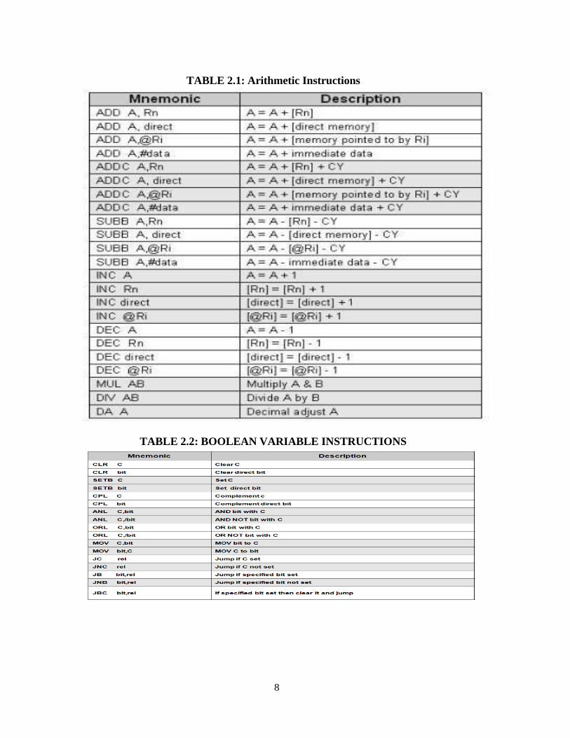
TABLE 2.1: Arithmetic Instructions
TABLE 2.2: BOOLEAN VARIABLE INSTRUCTIONS
9
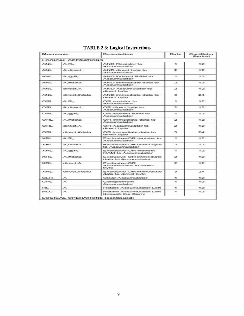
TABLE 2.3: Logical Instructions

10
TABLE 2.4: Data transfer Instructions

11
TABLE 2.5: PROGRAM BRANCH INSTRUCTIONS
Direct bit addressing
Values between 0 and 127 (00H and 7FH) define bits in a block of 16 bytes of on-
chip RAM between addresses 20H-2FH. They are numbered consecutively from
the lowest-order bytes lowest order bit through the highest order bit.
Bit addresses between 128 and 255 (80H and 0FFH) correspond to bits in a number
of special function registers mostly used for I/O or peripheral device control. These
positions are numbered with a different scheme than RAM. The five high-order
address bits match those of the registers own address
while the three low-order bits identifies the bit position within that register.

12
Read Write Read
AReg Ext
MOVX @ RT RAM
R0 or R1
Int & Ext
RAM
MOVX @ DPTR DPTR
DPTR +A
PC+ A
MOVCA,@ A+PC
External Addressing using MOVX and MOVE
Fig 2.5: External Addressing using MOVX and MOVE
Jump and Call Program Range
Relative Range:
Jump that replaces the program counter content with a new address that is greater
than the ad- dress of the instruction following the jump by 127 or less than the
address of the instruction following jump by 128 are called relative jumps. The
address following the jump is used to calculate the relative jump because the PC is
incremented to the next instruction before the current instruction is extended.
Relative jump has two advantages. First, only 1 byte of data (2‗s complement)
need to be speci- fied for jumping ahead(positive range 0-127) or jumping back
(negative range -128). Specifying only 1 byte saves program bytes and speeds up
program execution. Second, the program that is written using relative jumps can be
relocated anywhere in the program namely without reassembling the code to
generate absolute addresses.
The disadvantage of relative jump is the short jump range (-128 to 127). This can
be problem- atic in large programs where multiple relative jump may be require
if higher jump range is required. Instructions using relative range jump are SJMP
rel, and all conditional jumps.

13
Short Absolute Range:
Short Absolute range makes use of the concept of dividing memory into logical
divisions called pages. Program memory may be regarded as one continuous stretch
of addresses from 0000H to 0FFFFH or it can be divided into a series of pages of
any convenient binary size.
The 8051 program memory is arranged on 2k byte pages giving a total of 32 (20H)
pages. The hexadecimal address of each page is shown in the following table.
TABLE 2.6:8051 2K Pages
Page Address Range Page Address Range
00 0000 - 07FF 10 8000 - 87FF
01 0800 - 0FFF 11 8800 - 8FFF
02 1000 - 17FF 12 9000 - 97FF
03 1800 - 1FFF 13 9800 - 9FFF
04 2000 - 27FF 14 A000 - A7FF
05 2800 - 2FFF 15 A800 - AFFF
06 3000 - 37FF 16 B000 - B7FF
07 3800 - 3FFF 17 B800 - BFFF
08 4000 - 47FF 18 C000 - C7FF
09 4800 - 4FFF 19 C800 - CFFF
0A 5000 - 57FF 1A D000 - D7FF
0B 5800 - 5FFF 1B D800 - DFFF
0C 6000 - 67FF 1C E000 - E7FF
0D 6800 - 6FFF 1D E800 - EFFF
0E 7000 - 77FF 1E F000 - F7FF
0F 7800 - 7FFF 1F F800 - FFFF
It can be seen that the upper 5 bits of the program counter hold the page number
and the lower 11 bits of the program counter hold the address within each page.
Thus an absolute address is formed by taking page number of the instruction
following the branch and attaching the absolute page range address of 11 bits to it
to form the 16-bit address.
Difficulty is encountered when the next instruction (the instruction following the
jump instruction) starts at X800H or X000H. This places the jump or call address
on the same page as the next in- struction. This does not give rise to any problem
on forward jump, but results in error if the branch is backward in the program. This
should be checked by assembler and the user should be instructed to relocate the

14
program suitably.
Short absolute range jump is also relocatable as the relative jump. Instructions
using short abso- lutes range are
ACALL addr 11
AJMP addr 11
Long Absolute Jump:
Address that can access the entire program from 0000H to FFFFH use long-range
addressing. Long range addresses require more bytes of code to specify and
relocatable only at the beginning of 64 K byte pages. Since the normal code
memory is only 64k bytes, the program must be reassembled every time a long-
range address changes and then branches are not generally relocatable.
Instructions using long absolute range are LCALL addr 16
LJMP addr 16
JMP @ A+DPTR
8051 MICROCONTROLLER PROGRAMS
.8 BIT ADDITION USING INTERNAL MEMORY
Mnemonics
Opcode Operand Comments
MOV A,40 Move the content of 40 to accumulator
MOV R0,41 Move the content of 41 to ‗R0‗ register
ADD A,R0 Add the content of ‗R0‗ and ‗A‗
MOV 42,A Move the content of accumulator to 42
MOV A,#00 Initialize the accumulator
ADDC A,#00 Add the content of A and 00 with carry MOV 43,A Move the content of accumulator to 43 LCALL 00BB Halt the program

15
8 BIT ADDITION USING EXTERNAL MEMORY
Mnemonics
Opcode Operand Comments
MOV DPTR,#9100 Initialize the data pointer
MOVX A,@DPTR Move the content of DPTR to Acc.
MOV R0,A Move the content of A to R0
INC DPTR Increment the data pointer
MOVX A,@DPTR Move the content of DPTR to Acc.
ADD A,R0 Add the content of ‗R0‗ and ‗A‗
INC DPTR Increment the data pointer
MOVX @DPTR,A Move the content of A to DPTR
MOV A,#00 Initialize the accumulator
ADDC A,#00 Add the content of A and 00 with carry
INC DPTR Increment the data pointer
MOVX @DPTR,A Move the content of A to DPTR LCALL 00BB Halt the program

16
8 BIT SUBTRACTION USING INTERNAL MEMORY
Mnemonics
Opcode Operand Comments
CLR C Clear the Carry flag
MOV A,40 Move the content of 40 to accumulator
MOV R0,41 Move the content of 41 to ‗R0‗ register
SUBB A,R0 Subtract the content of ‗R0‗ from ‗A‗
MOV 42,A Move the content of accumulator to 42
MOV A,#00 Initialize the accumulator
ADDC A,#00 Add the content of A and 00 with carry MOV 43,A Move the content of accumulator to 43 LCALL 00BB Halt the program
8 BIT SUBTRACTION USING EXTERNAL MEMORY
Mnemonics
Opcode Operand Comments
CLR C Clear the Carry flag MOV DPTR,#9100 Initialize the data pointer
MOVX A,@DPTR Move the content of DPTR to Acc.
MOV R0,A Move the content of A to R0
INC DPTR Increment the data pointer
MOVX A,@DPTR Move the content of DPTR to Acc.
SUBB A,R0 Subtract the content of ‗R0‗ from ‗A‗ INC DPTR Increment the data pointer
MOVX @DPTR,A Move the content of A to DPTR
MOV A,#00 Initialize the accumulator
ADDC A,#00 Add the content of A and 00 with carry
INC DPTR Increment the data pointer MOVX @DPTR,A Move the content of A to DPTR LCALL 00BB Halt the program
8 BIT MULTIPLICATION USING INTERNAL MEMORY
Mnemonics
Opcode Operand Comments
MOV A,40 Move the content of 40 to accumulator
MOV 0F0,41 Move the content of 41 to ‗B‗ register MUL AB Multiply the content of ‗A‗ and ‗B‗
MOV 42,A Move the content of accumulator to 42
MOV A,0F0 Move the content of ‗B‗ to accumulator MOV 43,A Move the content of accumulator to 43 LCALL 00BB Halt the program

17
8 BIT MULTIPLICATION USING EXTERNAL MEMORY
Mnemonics
Opcode Operand Comments
MOV DPTR,#9100 Initialize the data pointer
MOVX A,@DPTR Move the content of DPTR to Acc. MOV 0F0,A Move the content of ‗A‗ to ‗B‗ register
INC DPTR Increment the data pointer
MOVX A,@DPTR Move the content of DPTR to Acc.
MUL AB Multiply the content of ‗A‗ and ‗B‗
INC DPTR Increment the data pointer MOVX @DPTR,A Move the content of ‗A‗ to DPTR
MOV A,0F0 Move the content of ‗B‗ to accumulator
INC DPTR Increment the data pointer
MOVX @DPTR,A Move the content of A to DPTR LCALL 00BB Halt the program
8 BIT DIVISION USING INTERNAL MEMORY
Mnemonics
Opcode Operand Comments
MOV A,40 Move the content of 40 to accumulator
MOV 0F0,41 Move the content of 41 to ‗B‗ register DIV AB Divide the content of ‗A‗ and ‗B‗
MOV 42,A Move the content of accumulator to 42
MOV A,0F0 Move the content of ‗B‗ to accumulator
MOV 43,A Move the content of accumulator to 43 LCALL 00BB Halt the program
8 BIT DIVISION USING EXTERNAL MEMORY
Mnemonics
Opcode Operand Comments
MOV DPTR,#9100 Initialize the data pointer
MOVX A,@DPTR Move the content of DPTR to Acc. MOV 0F0,A Move the content of ‗A‗ to ‗B‗ register
INC DPTR Increment the data pointer
MOVX A,@DPTR Move the content of DPTR to Acc.
DIV AB Divide the content of ‗A‗ and ‗B‗
INC DPTR Increment the data pointer MOVX @DPTR,A Move the content of ‗A‗ to DPTR

18
MOV A,0F0 Move the content of ‗B‗ to accumulator
INC DPTR Increment the data pointer
MOVX @DPTR,A Move the content of A to DPTR
LCALL 00BB Halt the program

19
16 BIT ADDITION USING INTERNAL MEMORY
Mnemonics
Opcode Operand Comments
MOV A,40 Move the content of 40 to accumulator MOV R0,A Move the content of ‗A‗ to ‗R0‗ register
MOV A,41 Move the content of 41 to accumulator
MOV R1,A Move the content of ‗A‗ to ‗R1‗ register
MOV A,42 Move the content of 42 to accumulator
MOV R2,A Move the content of ‗A‗ to ‗R2‗ register
MOV A,43 Move the content of 43 to accumulator
MOV R3,A Move the content of ‗A‗ to ‗R3‗ register
MOV A,R0 Move the content of ‗ R0‗ to ‗A‗ register
ADD A,R2 Add the content of ‗R2‗ and ‗A‗
MOV 44,A Move the content of ‗A‗ to 44 Mem. Loc
MOV A,R1 Move the content of R1 to accumulator
ADDC A,R3 Add the content of ‗R3‗ and ‗A‗ with carry
MOV 45,A Move the content of ‗A‗ to 45 Mem. Loc.
MOV A,#00 Initialize the accumulator ADDC A,#00 Add the content of A and 00 with carry
MOV 46,A Move the content of ‗A‗ to 46 Mem. Loc.
LCALL 00BB Halt the program
16 BIT ADDITION USING EXTERNAL MEMORY
Mnemonics
Opcode Operand Comments
MOV DPTR,#9100 Initialize the data pointer
MOVX A,@DPTR Move the content of DPTR to Acc. MOV R0,A Move the content of ‗ A‗ to ‗R0‗ register
INC DPTR Increment the data pointer
MOVX A,@DPTR Move the content of DPTR to Acc.
MOV R1,A Move the content of ‗ A‗ to ‗R1‗ register
INC DPTR Increment the data pointer
MOVX A,@DPTR Move the content of DPTR to Acc. MOV R2,A Move the content of ‗ A‗ to ‗R2‗ register
INC DPTR Increment the data pointer
MOVX A,@DPTR Move the content of DPTR to Acc.
MOV R3,A Move the content of ‗ A‗ to ‗R3‗ register
MOV A,R0 Move the content of ‗ R0‗ to ‗A‗ register
ADD A,R2 Add the content of ‗R2‗ and ‗A‗ INC DPTR Increment the data pointer
MOVX @DPTR,A Move the content of A to DPTR
MOV A,R1 Move the content of ‗ R1‗ to ‗A‗ register
ADDC A,R3 Add the content of ‗R3‗ and ‗A‗ with carry
INC DPTR Increment the data pointer
MOVX @DPTR,A Move the content of A to DPTR MOV A,#00 Initialize the accumulator

20
ADDC A,#00 Add the content of A and 00 with carry
INC DPTR Increment the data pointer MOVX @DPTR,A Move the content of A to DPTR LCALL 00BB Halt the program

21
BCD ADDITION USING INTERNAL MEMORY
Mnemonics
Opcode Operand Comments
MOV A, #47h first BCD operand MOV R0,A Move A to R0 MOV A, #25h second BCD operand
ADD A,R0 Add the content of ‗R0‗ and ‗A‗ (A=6Ch)
DA A Decimal adjust accumulator (A=72h)
MOV 40,A Move the content of accumulator to 40 LCALL 00BB Halt the program
Hex BCD 47 0100 0111
+ 25 + 0010 0101
6C
0110 1100
+ 6 + 0110
72
0111 0010
TEXT / REFERENCE BOOKS
1. Kenneth. J. Ayala, ―The 8051 Microcontroller Architecture, Programming and Apllications‖, Penram
International, 1996, 2 nd Edition.
2. Sriram. V. Iyer, Pankaj Gupta, ―Embedded Real Time Systems Programming‖, 2004 Tata McGraw Hill
Publishing Company Limited, 2006.
3. Frank Vahid, Tony Givargis, ‗Embedded system Design - A unified Hardware / software Introduction‘,
John Wiley and Sons, 2002.
4. Todd D Morton, ‗Embedded Microcontrollers‘, Reprint by 2005, Low Price Edition.
5. Muhammed Ali Mazidi, Janice Gillispie Mazidi, ‗The 8051 Microcontroller and Embedded Systems‘,
Low Price Edition, Second Impression 2006.
6. Raj Kamal, ‗Embedded Systems-Architecture, Programming and Design‘, Tata McGraw Hill
Publishing Company Limited 2003.
7. Muhammed Ali Mazidi, Rolin D.Mckinlay, Dannycauscy, ―PIC microcontrollers and embedded
systems using assembly and C‖, 1st edition, Pearson, 2007.

1
PRINCIPLES OF EMBEDDED SYSTEM DESIGN-SECA1706
SCHOOL OF ELECTRICAL AND ELECTRONICS
DEPARTMENT OF ELECTRICAL AND ELECTRONICS ENGINEERING

2
UNIT-III
RISC EMBEDDED CONTROLLERS

3
III. UNIT III RISC EMBEDDED CONTROLLERS
SYLLABUS:
Comparison of CISC and RISC controllers - PIC 16F877 architecture - Memory organization -
Addressing modes - Assembly language instructions. Arm 7 Processor-Register Organization-Modes &
Status.
Table 3.1-Comparison of RISC and CISC processors
RISC CISC
Acronym It stands for ‗Reduced Instruction Set Computer‗.
It stands for ‗Complex Instruction Set Computer‗
Definition processors have a smaller set of
instructions with few addressing nodes.
Processors have a larger set of instructions
with many addressing nodes.
Memory unit It has no memory unit and uses a
separate hardware to implement
instructions.
It has a memory unit to implement complex
instructions
Program It has a hard-wired unit of programming.
It has a microprogramming unit.
Design It is a complex complier design. It is an easy complier design
Calculations The calculations are faster and precise. The calculations are slow and precise.
Time Execution time is very less. Execution time is very high
External memory
It does not require external memory for calculations.
It requires external memory for calculations.
Pipelining Pipelining does function correctly. Pipelining does not function correctly.
Stalling Stalling is mostly reduced in
processors.
The processors often stall
Code expansion
Code expansion can be a problem. Code expansion is not a problem.
Disc space The space is saved. The space is wasted.
Applications Used in high end applications such as video processing, telecommunications and image
Used in low end applications such as security
Salient features of PIC 16F877A Microcontroller
4
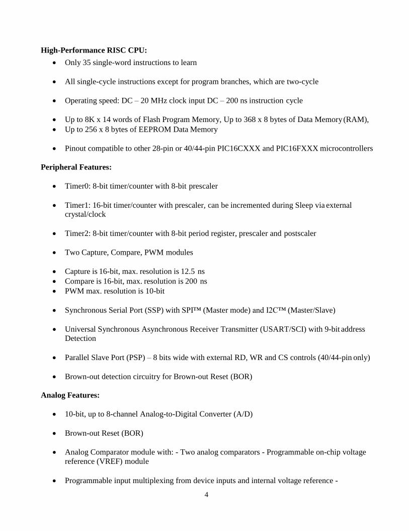
High-Performance RISC CPU:
Only 35 single-word instructions to learn
All single-cycle instructions except for program branches, which are two-cycle
Operating speed: DC – 20 MHz clock input DC – 200 ns instruction cycle
Up to 8K x 14 words of Flash Program Memory, Up to 368 x 8 bytes of Data Memory (RAM),
Up to 256 x 8 bytes of EEPROM Data Memory
Pinout compatible to other 28-pin or 40/44-pin PIC16CXXX and PIC16FXXX microcontrollers
Peripheral Features:
Timer0: 8-bit timer/counter with 8-bit prescaler
Timer1: 16-bit timer/counter with prescaler, can be incremented during Sleep via external crystal/clock
Timer2: 8-bit timer/counter with 8-bit period register, prescaler and postscaler
Two Capture, Compare, PWM modules
Capture is 16-bit, max. resolution is 12.5 ns
Compare is 16-bit, max. resolution is 200 ns
PWM max. resolution is 10-bit
Synchronous Serial Port (SSP) with SPI™ (Master mode) and I2C™ (Master/Slave)
Universal Synchronous Asynchronous Receiver Transmitter (USART/SCI) with 9-bit address
Detection
Parallel Slave Port (PSP) – 8 bits wide with external RD, WR and CS controls (40/44-pin only)
Brown-out detection circuitry for Brown-out Reset (BOR)
Analog Features:
10-bit, up to 8-channel Analog-to-Digital Converter (A/D)
Brown-out Reset (BOR)
Analog Comparator module with: - Two analog comparators - Programmable on-chip voltage
reference (VREF) module
Programmable input multiplexing from device inputs and internal voltage reference -
5
Comparator outputs are externally accessible
Special Microcontroller Features:
100,000 erase/write cycle Enhanced Flash program memory typical• 1,000,000 erase/write cycle Data EEPROM memory typical
Data EEPROM Retention > 40 years
Self-reprogrammable under software control
In-Circuit Serial Programming™ (ICSP™) via two pins
Single-supply 5V In-Circuit Serial Programming
Watchdog Timer (WDT) with its own on-chip RC oscillator for reliable operation •
Programmable code protection
Power saving Sleep mode • Selectable oscillator options
In-Circuit Debug (ICD) via two pins
CMOS Technology:
Low-power, high-speed Flash/EEPROM technology
Fully static design
Wide operating voltage range (2.0V to 5.5V)
Commercial and Industrial temperature ranges
Low-power consumption
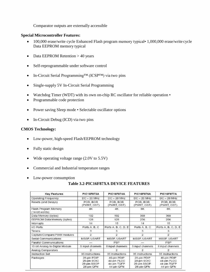
Table 3.2-PIC16F87XA DEVICE FEATURES

6
PIC 16F877A Pin Diagram and Description
Fig 3.1: PIC 16F877A Pin Diagram and Description
Pin diagram PIC16F877A The PIC 16F877 features all the components which modern
microcontrollers normally have The PIC16F provides 8K bytes of Flash, 368 bytes of RAM, 256 bytes
of EPROM, 5 I/O ports, 3 timers., 35 simple word instructions.

7
8
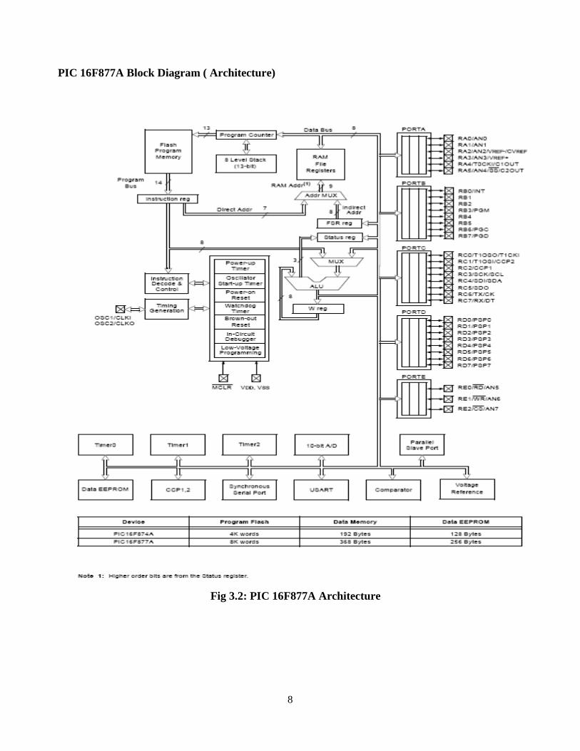
PIC 16F877A Block Diagram ( Architecture)
Fig 3.2: PIC 16F877A Architecture
9
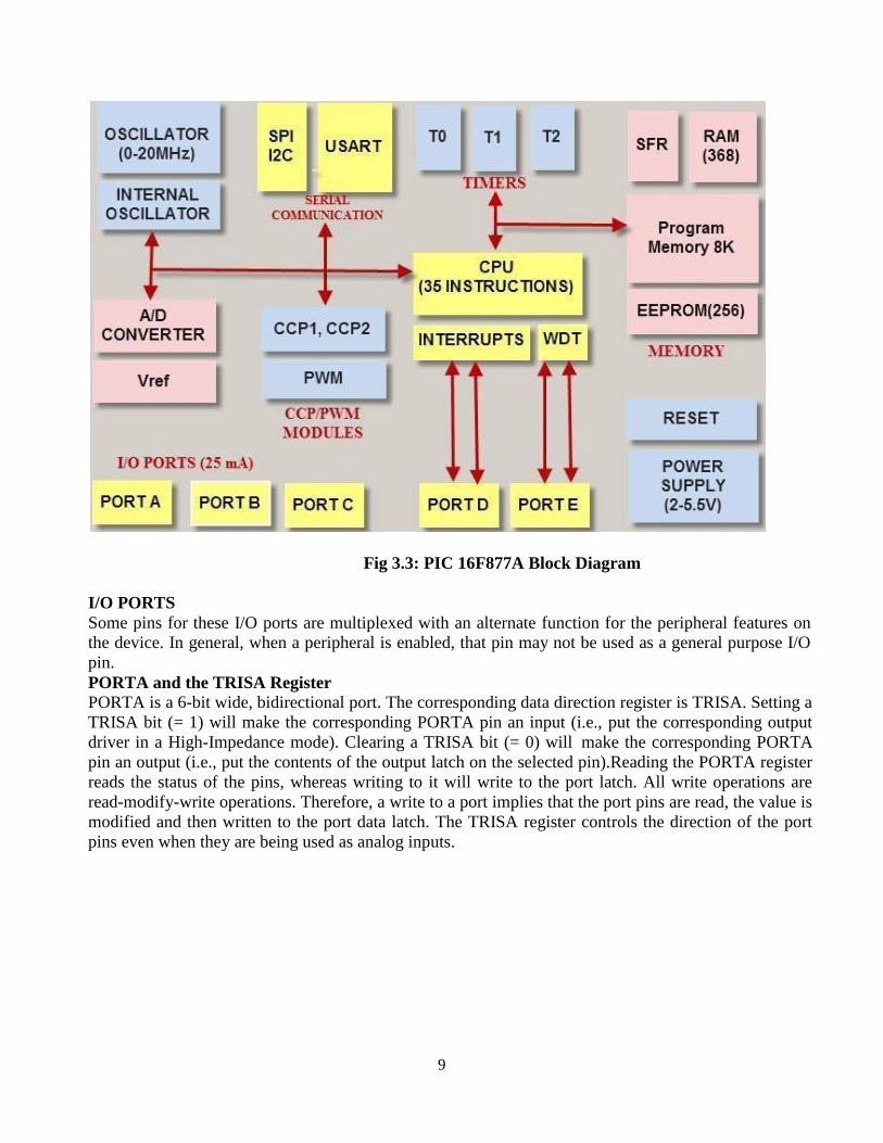
Fig 3.3: PIC 16F877A Block Diagram
I/O PORTS
Some pins for these I/O ports are multiplexed with an alternate function for the peripheral features on
the device. In general, when a peripheral is enabled, that pin may not be used as a general purpose I/O
pin.
PORTA and the TRISA Register
PORTA is a 6-bit wide, bidirectional port. The corresponding data direction register is TRISA. Setting a
TRISA bit (= 1) will make the corresponding PORTA pin an input (i.e., put the corresponding output
driver in a High-Impedance mode). Clearing a TRISA bit (= 0) will make the corresponding PORTA
pin an output (i.e., put the contents of the output latch on the selected pin).Reading the PORTA register
reads the status of the pins, whereas writing to it will write to the port latch. All write operations are
read-modify-write operations. Therefore, a write to a port implies that the port pins are read, the value is
modified and then written to the port data latch. The TRISA register controls the direction of the port
pins even when they are being used as analog inputs.

10
Fig 3.4: PORT A
Similarly for other ports : PORTB and the TRISB Register ,PORTC and the TRISC Register, PORTD and TRISD Registers ,PORTE and TRISE Register.
TIMER0 MODULE
The Timer0 module timer/counter has the following features:
8-bit timer/counter
Readable and writable
8-bit software programmable prescaler
Internal or external clock select
Interrupt on overflow from FFh to 00h
Edge select for external clock
The Timer1 module is a 16-bit timer/counter consisting of two 8-bit registers (TMR1H and TMR1L)
which are readable and writable. Timer1 can operate in one of two modes:
As a Timer
As a Counter
Timer2 is an 8-bit timer with a prescaler and a postscaler. It can be used as the PWM time base for the
PWM mode of the CCP module(s). The TMR2 register is readable and writable and is cleared on any
device Reset.
CAPTURE/COMPARE/PWM MODULES

11
Each Capture/Compare/PWM (CCP) module contains a 16-bit register which can operate as a:
16-bit Capture register
16-bit Compare register
PWM Master/Slave Duty Cycle register
CCP1 Module:
Capture/Compare/PWM Register 1 (CCPR1) is comprised of two 8-bit registers: CCPR1L (low byte)
and CCPR1H (high byte). The CCP1CON register controls the operation of CCP1. The special event
trigger is generated by a compare match and will reset Timer1.
CCP2 Module:
Capture/Compare/PWM Register 2 (CCPR2) is comprised of two 8-bit registers: CCPR2L (low byte)
and CCPR2H (high byte). The CCP2CON register controls the operation of CCP2. The special event
trigger is generated by a compare match and will reset Timer1 and start an A/D conversion (if the A/D
module is enabled).
Capture Mode
In Capture mode, CCPR1H:CCPR1L captures the 16-bit value of the TMR1 register when an event
occurs on pin RC2/CCP1. An event is defined as one of the following:
Every falling edge
Every rising edge
Every 4th rising edge
Every 16th rising edge
The type of event is configured by control bits, CCP1M3:CCP1M0 (CCPxCON<3:0>).
Compare Mode
In Compare mode, the 16-bit CCPR1 register value is constantly compared against the TMR1 register
pair value. When a match occurs, the RC2/CCP1 pin is:
Driven high
Driven low
Remains unchanged
The action on the pin is based on the value of control bits, CCP1M3:CCP1M0 (CCP1CON<3:0>).
PWM Mode (PWM)
In Pulse Width Modulation mode, the CCPx pin produces up to a 10-bit resolution PWM output.
PWM BLOCK DIAGRAM

12
Fig 3.5: PWM BLOCK DIAGRAM
Master SSP (MSSP) Module
The Master Synchronous Serial Port (MSSP) module is a serial interface, useful for communicating
with other peripheral or microcontroller devices. These peripheral devices may be serial EEPROMs,
shift registers,display drivers, A/D converters, etc. The MSSP module can operate in one of two modes:
Serial Peripheral Interface (SPI)
Inter-Integrated Circuit (I2C)
Full Master mode
Slave mode (with general address call)
The I2C interface supports the following modes in hardware:
Master mode
Multi-Master mode
Slave mode
COMPARATOR MODULE
The comparator module contains two analog comparators.The inputs to the comparators are multiplexed
with I/O port pins RA0 through RA3, while the outputs are multiplexed to pins RA4 and RA5.
Reset
The PIC16F87XA differentiates between various kinds of Reset:
Power-on Reset (POR)
MCLR Reset during normal operation
MCLR Reset during Sleep
WDT Reset (during normal operation)
WDT Wake-up (during Sleep)
Brown-out Reset (BOR)0
Memory organization

13
The program memory and data memory have separate buses so that concurrent access can occur
Program memory map
The PIC16F87XA devices have a 13-bit program counter capable of addressing an 8K word x 14
bit.program memory space. The PIC16F876A/877Adevices have 8K words x 14 bits of Flash program
memory. The Reset vector is at 0000h and the interrupt vector is at 0004h.
Fig 3.6: Program memory map
Data Memory Organization
The data memory is partitioned into multiple banks which contain the General Purpose Registers and
the Special Function Registers. Bits RP1 (Status<6>) and RP0 (Status<5>) are the bank select bits.
Each bank extends up to 7Fh (128 bytes). The lower locations of each bank are reserved for the Special
Function Registers. Above the Special Function Registers are General Purpose Registers, implemented

14
as static RAM. All implemented banks contain Special Function Registers.
Data EEPROM and flash program memory
The data EEPROM and Flash program memory is readable and writable during normal operation (over
the full VDD range). This memory is not directly mapped in the register file space. Instead, it is
indirectly addressed through the Special Function Registers. There are six SFRs used to read and write
this memory:
EECON1
EECON2
EEDATA
EEDATH
EEADR
EEADRH
GENERAL PURPOSE REGISTER FILE
The register file can be accessed either directly, or indirectly, through the File Select Register (FSR).
SPECIAL FUNCTION REGISTERS
The Special Function Registers are registers used by the CPU and peripheral modules for controlling
the desired operation of the device. These registers are implemented as static RAM. The Special
Function Registers can be classified into two sets: core (CPU) and peripheral. Some examples are
Status Register The Status register contains the arithmetic status of the ALU, the Reset status and the
bank select bits for data memory.
• STATUS register – changes/moves from/between the banks
• PORT registers – assigns logic values (―0‖/‖1‖) to the ports
• TRIS registers - data direction register (input/output)
DIRECT/INDIRECT ADDRESSING
1. Direct addressing
Direct addressing like CLRF 13h. We deal with the address or the memory location.
Direct Addressing is done through a 9-bit address. This address is obtained by connecting 7th bit
of direct address. By using an instruction with two bits (RP1, RP0) from STATUS register. this is
shown on bellow Figure . Any access to SFR registers can be an example of direct addressing.

15
Fig 3.7: Direct Addressing Mode
2. Indirect Addressing, INDF and FSR Registers
The INDF register is not a physical register. Addressing the INDF register will cause indirect
addressing. Indirect addressing is possible by using the INDF register. Any instruction using the INDF
register actually accesses the register pointed to by the File Select Register, FSR. Reading the INDF
register itself, indirectly (FSR = 0) will read 00h. Writing to the INDF register indirectly results in a no
operation (although status bits may be affected). An effective 9-bit address is obtained by concatenating
the 8-bit FSR register and the IRP bit
Fig 3.8: Indirect Addressing Mode
INSTRUCTION SET SUMMARY
The PIC16 instruction set is highly orthogonal and is comprised of three basic categories:
Byte-oriented operations
Bit-oriented operations
Literal and control operations.
16
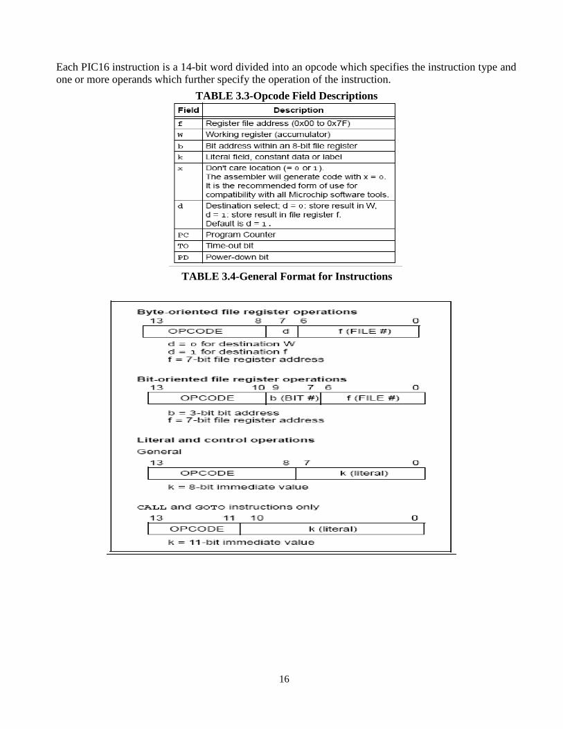
Each PIC16 instruction is a 14-bit word divided into an opcode which specifies the instruction type and one or more operands which further specify the operation of the instruction.
TABLE 3.3-Opcode Field Descriptions
TABLE 3.4-General Format for Instructions
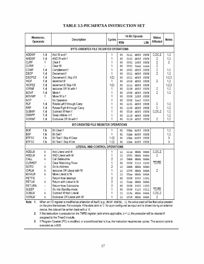
17
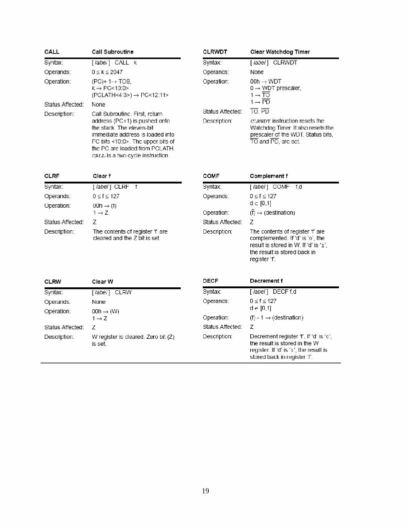
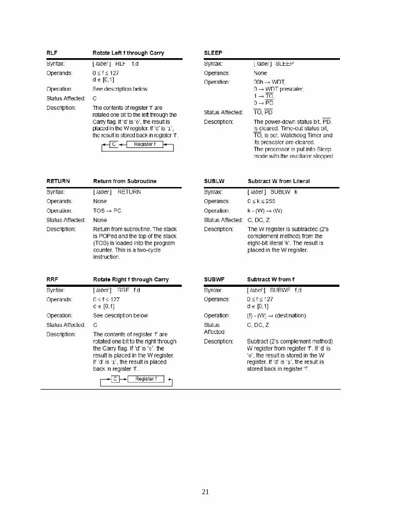
TABLE 3.5-PIC16F87XA INSTRUCTION SET

18
19

20
21

22
History of the ARM Processor
Developed the first ARM Processor (Acorn RISC Machine) in 1985 at Acorn Computers
Limited.
• Established a new company named Advanced RISCMachine Limited and developed
ARM6.
• Continuation of the architecture enhancements from the original architecture
Features of the ARM Processor
Incorporate features of Berkeley RISC design
a large register file
a load/store architecture
uniform and fixed length instruction field

23
simple addressing mode
Other ARM architecture features
Arithmetic Logic Unit and barrel shifter
auto increment and decrement addressing mode
conditional execution of instructions
o Based on Von Neumann Architecture or Harvard Architecture
The Evolution of the ARM architecture:
Fig 3.9: The Evolution of the ARM architecture

24
Architecture V1 was implemented only in the ARM1 CPU and was not utilized in a
commercial product. Architecture V2 was the basis for the first shipped processors. These two
architectures were developed by Acorn Computers before ARM became a company in 1990.
After that introduced ARM the Architecture V3, which included many changes over its
predecessors .These changes resulted in an extremely small and power-efficient processor suitable
for embedded systems .Architecture V4, co-developed by ARM and Digital Electronics
Corporation, resulted in the Strong ARM series of processors. These processors are very
performance-centric and do not include the on chip debug extensions.
This architecture was further developed to include the Thumb 16-bitinstruction set
architecture enabling a 32-bit processor to utilize a 16-bit system. Today, ARM only licenses
cores based on Architecture V4T or above.
The latest architectures, version 5TE and 5TEJ, embody added instructions for DSP
applications and the Jazelle-Java extensions, respectively.
Currently, the ARM9E and 10E family of processors are the only implementations of
these architectures. Details on these architectures and cores will be provided later in the course.
Architecture basics
ARM cores use a 32-bit, Load-Store RISC architecture. That means that the core cannot
directly manipulate the memory. All data manipulation must be done by loading registers with
information located in memory, performing the data operation and then storing the value back to
memory. There are 37 total registers in the processor. However, that number is split among seven
different processor modes. The seven processor modes are used to run user tasks, an operating
system, and to efficiently handle exceptions such as interrupts. Some of the registers within each
mode are reserved for specific use by the core, while most are available for general use. The
reserved registers that are used by the core for specific functions are r13 is commonly used as the
stack pointer (SP), r14 as a link register (LR), r15as a program counter (PC), the Current Program
Status Register (CPSR), and the Saved Program Status Register (SPSR).
The SPSR and the CPSR contain the status and control bits specific to the properties the processor
core is operating under. These properties define the operating mode, ALU status flags, interrupt
disable/enable flags and whether the core is operating in 32-bit ARM or 16-bit Thumb state.
There are 37 total registers divided among seven different processor modes. Figure 09
shows thebank of registers visible in each mode .User mode, the only non-privileged mode, has
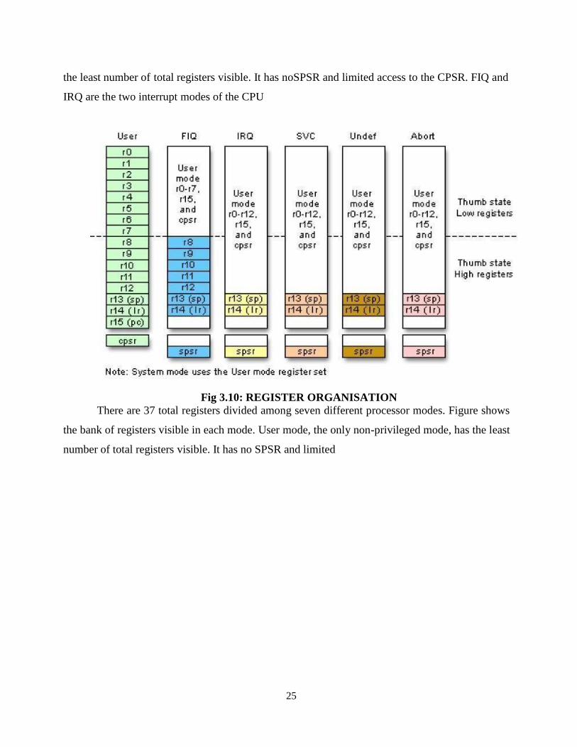
25
the least number of total registers visible. It has noSPSR and limited access to the CPSR. FIQ and
IRQ are the two interrupt modes of the CPU
Fig 3.10: REGISTER ORGANISATION
There are 37 total registers divided among seven different processor modes. Figure shows
the bank of registers visible in each mode. User mode, the only non-privileged mode, has the least
number of total registers visible. It has no SPSR and limited

26
access to the CPSR. FIQ and IRQ are the two interrupt modes of the CPU.
Supervisor mode is the default mode of the processor on start up or reset. Undefined mode traps
unknown or illegal instructions when they are passed though the pipeline. Abort mode traps
illegal memory accesses as a result of fetching instructions or accessing data.
Finally, system mode, which uses the user mode bank of registers, was introduced to provide an
additional privileged mode when dealing with nested interrupts.
Each additional mode offers unique registers that are available for use by exception handling
routines. These additional registers are the minimum number of registers required to preserve the
state of the processor, save the location in code, and switch between modes.
FIQ mode, however, has an additional five banked registers to provide more flexibility and
higher performance when handling critical interrupts.
When the ARM core is in Thumb state, the registers banks are split into low and high
register domains. The majority of instructions in Thumb state have a 3-bit register specifier. As a
result, these instructions can only access the low registers in Thumb, R0 through R7. The high
registers,R8through R15, have more restricted use. Only a few instructions have access to these
registers.
TDMI stands for:
• Thumb, which is a 16-bit instruction set extension to the 32-bit ARM architecture, referred as
states of the processor.
• "D" and "I" together comprise the on-chip debug facilities offered on all ARM cores.These
stand for the Debug signals and EmbeddedICE logic, respectively.
• The M signifies the support for 64-bit results and an enhanced multiplier, resulting inhigher
performance. This multiplier is now standard on all ARMv4 architectures and\above.
Thumb 16-bit Instructions
With growing code and data size, memory contributes to the system cost. The need to
reduce memorycost leads to smaller code size and the use of narrower memory. Therefore ARM
developed a modified instruction set to give market-leading code density for compiled standard C
language.
There is also the problem of performance loss due to using a narrow memory path, such as
a 16-bitmemory path with a 32-bit processor.

27
The processor must take two memory access cycles to fetch an instruction or read and write data.
To address this issue, ARM introduced another set of reduced 16-bit instructions labeled Thumb,
based on the standard ARM 32-bit instruction set.
For Thumb to be used, the processor must go through a change of state from ARM to Thumb in
order to begin executing 16-bit code. This is because the default state of the core is ARM.
Therefore, every application must have code at boot up that is written in ARM. If the application
code is to be compiled entirely for Thumb, then the segment of ARM boot code must change the
state of the processor. Once this is done, 16-bit instructions are fetched seamlessly into the
pipeline without any result.
It is important to note that the architecture remains the same. The instruction set is actually a
reduced set of the ARM instruction set and only the instructions are 16-bit; everything else in the
core still operates as 32-bit.An application code compiled in Thumb is 30% smaller on average
than the same code compiled in ARM and normally 30% faster when using narrow 16-bit memory
systems.
Fig 3.10: Register Bank in the
center of the diagram
FIGURE shows the register bank in the center of the diagram, plus the required address bus

28
and data bus. The multiplier, in-line barrel shifter, and ALU are also shown. In addition, the
diagram illustrates the in-line decompression process of Thumb instructions while in the decode
stage of the pipeline. This process creates a 32-bit ARM equivalent instruction from the 16-bit
Thumb instruction, decodes the instruction, and passes it on to the execute stage.
ARM design philosophy
Small processor for lower power consumption (for embedded system)
• High code density for limited memory and Physical size
restrictions
• The ability to use slow and low-cost memory
• Reduced die size for reducing manufacture cost and
accommodating more peripherals
Registers
ARM has 37 registers all of which are 32-bits long. 1 dedicated program counter
1 dedicated current program status register
5 dedicated saved program status registers
30 general purpose registers
The current processor mode governs which of several banks is accessible.
Each mode can access a particular set of
r0-r12 registers
a particular r13 (the stack pointer, sp)
r14 (the link register, lr)
the program counter, r15 (pc)
the current program status register, cpsr
Privileged modes (except System) can also access a particular spsr (saved program status

29
reg
Registers
The ARM1136JF-S processor has a total of 37 registers:
• 31 general-purpose 32-bit registers
• six 32-bit status registers.
These registers are not all accessible at the same time. The processor state and operating mode
determine which registers are available to the programmer
The ARM state register set In ARM state, 16 general registers and one or two status
registers are accessible at any time. In privileged modes, mode-specific banked registers become
available.
The ARM state register set contains 16 directly-accessible registers, r0-r15. Another
register, the Current Program Status Register (CPSR), contains condition code flags, status bits,
and current mode bits. Registers r0-r13 are general-purpose registers used to hold either data or
address values. Registers r14, r15, and the SPSR have the following special functions.
Link Register Register r14 is used as the subroutine Link Register (LR). Register r14
receives the return address when a Branch with Link (BL or BLX) instruction is executed. You
can treat r14 as a general-purpose register at all other times. The corresponding banked registers
r14_svc, r14_irq, r14_fiq, r14_abt, and r14_und are similarly used to hold the return values when
interrupts and exceptions arise, or when BL or BLX instructions are executed within interrupt or
exception routines.
Program Counter Register r15 holds the PC:
• in ARM state this is word-aligned
• in Thumb state this is halfword-aligned
• in Java state this is byte-aligned. Saved Program Status Register
In privileged modes, another register, the Saved Program Status Register (SPSR), is
accessible. This contains the condition code flags, status bits, and current mode bits saved as a
result of the exception that caused entry to the current mode.
Banked registers have a mode identifier that indicates which mode they relate to. These mode

30
identifiers are listed in
Table 3.6-Register mode identifiers
FIQ mode has seven banked registers mapped to r8–r14 (r8_fiq– r14_fiq). As a result many FIQ
handlers do not have to save any registers. The Supervisor, Abort, IRQ, and Undefined modes each
have alternative mode-specific registers mapped to r13 and r14, permitting a private stack pointer and
link register for each mode
ARM Processor Modes
Unprivileged mode
User mode Privileged mode Abort mode
Fast Interrupt Request mode
Interrupt Request mode Supervisor mode
System mode
Undefined mode

31
Fig 3.11:register set showing banked registers

32
Fig 3.12: ARM register
The Thumb state register set
The Thumb state register set is a subset of the ARM state set. The programmer has direct access
to:
• Eight general registers, r0–r7
• The PC
• A stack pointer, SP (ARM r13)
• An LR (ARM r14)
• The CPSR.
There are banked SPs, LRs, and SPSRs for each privileged mode.
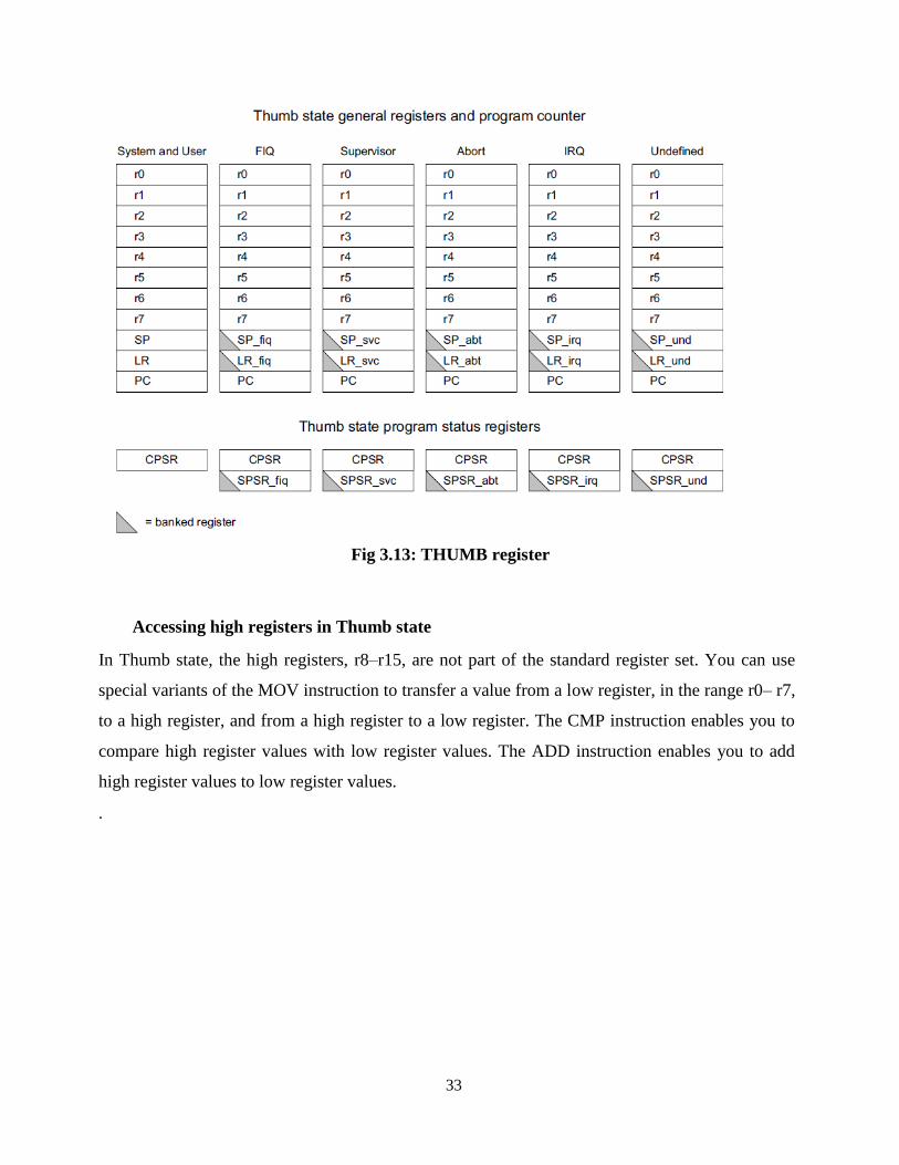
33
Fig 3.13: THUMB register
Accessing high registers in Thumb state
In Thumb state, the high registers, r8–r15, are not part of the standard register set. You can use
special variants of the MOV instruction to transfer a value from a low register, in the range r0– r7,
to a high register, and from a high register to a low register. The CMP instruction enables you to
compare high register values with low register values. The ADD instruction enables you to add
high register values to low register values.
.

34
ARM state and Thumb state registers relationship
Fig 3.14: ARM state and THUMB state registers relationship
Registers r0–r7 are known as the low registers. Registers r8–r15 are known as the
high registers.
The program status registers
The ARM7TDMI-S contains a CPSR and five SPSRs for
exception handlers to use. The
program status registers:
• hold the condition code flags
• control the enabling and disabling of interrupts
• set the processor operating mode.
The arrangement of bits is shown in Figure

35
Fig 3.15: Program Status Registers
The condition code flags
The N, Z, C, and V bits are the condition code flags, You can set these bits by arithmeticand
logical operations. The flags can also be set by MSR and LDM instructions.
TheARM7TDMI-S tests these flags to determine whether to execute an instruction.
All instructions can execute conditionally in ARM state. In Thumb state, only the Branch
instruction can be executed conditionally
The control bits
The bottom eight bits of a PSR are known collectively as the
control bits. They are the:

36
• Interrupt disable bits
• T bit
• Mode bits.
The control bits change when an exception occurs. When the processor is operating in a
privileged mode, software can manipulate these bits.
Interrupt disable bits
The I and F bits are the interrupt disable bits:
• when the I bit is set, IRQ interrupts are disabled
• when the F bit is set, FIQ interrupts are disabled.
T bit
The T bit reflects the operating state:
• when the T bit is set, the processor is executing in Thumbstate
• when the T bit is clear, the processor executing in ARMstate. The operating state is
reflected by the CPTBIT external signal.
Mode bits
The M4, M3, M2, M1, and M0 bits (M[4:0]) are the mode bits. These bits determine the processor
operating mode . Not all combinations of the mode bits define a valid processor mode, so take
care to use only the bit combinations shown
Reserved bits
The remaining bits in the PSRs are unused but are reserved. When changing a PSR flag or control
bits make sure that these reserved bits are not altered. Also, make sure that your program does not
rely on reserved bits containing specific values because future processors might have these bits set
to one or zero
The ARM7TDMI-S is a member of the ARM family of general- purpose 32-bit microprocessors.
The ARM family offers high performance for very low power consumption and gate count. The
ARM architecture is based on Reduced Instruction Set Computer (RISC) principles. The RISC
instruction set, and related decode mechanism are much simpler than those of Complex
Instruction Set Computer (CISC) designs. This simplicity gives:
• a high instruction throughput
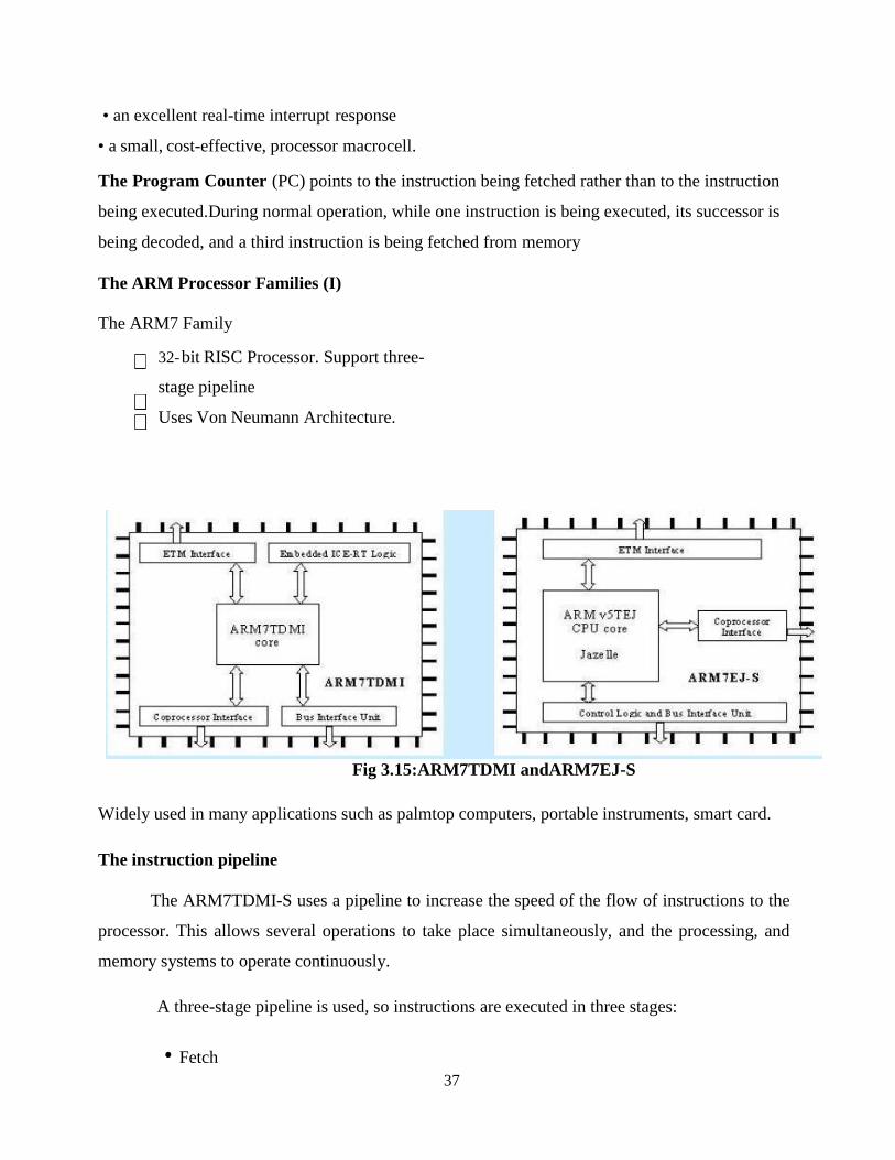
37
• an excellent real-time interrupt response
• a small, cost-effective, processor macrocell.
The Program Counter (PC) points to the instruction being fetched rather than to the instruction
being executed.During normal operation, while one instruction is being executed, its successor is
being decoded, and a third instruction is being fetched from memory
The ARM Processor Families (I)
The ARM7 Family
32- bit RISC Processor. Support three-
stage pipeline
Uses Von Neumann Architecture.
Fig 3.15:ARM7TDMI andARM7EJ-S
Widely used in many applications such as palmtop computers, portable instruments, smart card.
The instruction pipeline
The ARM7TDMI-S uses a pipeline to increase the speed of the flow of instructions to the
processor. This allows several operations to take place simultaneously, and the processing, and
memory systems to operate continuously.
A three-stage pipeline is used, so instructions are executed in three stages:
• Fetch

38
• Decode
• Execute.
The three-stage pipeline is shown in
ARM Pipelines
Pipeline mechanism to increase execution speed
• The pipeline design of each processor family is different

39
Fig 3.16:ARM7 Pipeline architecture

40
ARM 7 ARCHITECTURE
Fig 3.17:ARM7 DATAPATH OVERVIEW

41
A barrel shifter is a digital circuit that can shift a data word by a specified number of bits without
the use of any sequential logic, only pure combinational logic.
Fig 3.18: Barrel shifter

42
Fig 3.19: ARM 7 ARCHITECTURE
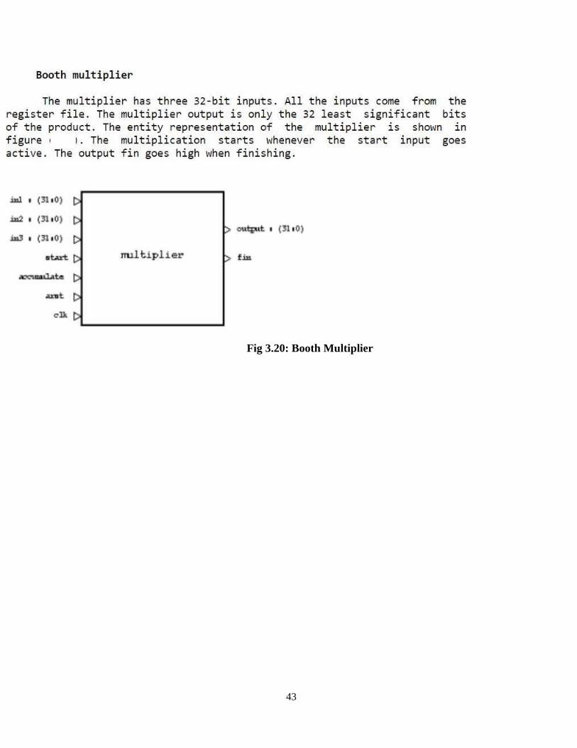
43
Fig 3.20: Booth Multiplier

44
TEXT / REFERENCE BOOKS
1. Kenneth. J. Ayala, ―The 8051 Microcontroller Architecture, Programming and Apllications‖, Penram
International, 1996, 2 nd Edition.
2. Sriram. V. Iyer, Pankaj Gupta, ―Embedded Real Time Systems Programming‖, 2004 Tata McGraw Hill
Publishing Company Limited, 2006.
3. Frank Vahid, Tony Givargis, ‗Embedded system Design - A unified Hardware / software Introduction‘,
John Wiley and Sons, 2002.
4. Todd D Morton, ‗Embedded Microcontrollers‘, Reprint by 2005, Low Price Edition.
5. Muhammed Ali Mazidi, Janice Gillispie Mazidi, ‗The 8051 Microcontroller and Embedded Systems‘,
Low Price Edition, Second Impression 2006.
6. Raj Kamal, ‗Embedded Systems-Architecture, Programming and Design‘, Tata McGraw Hill
Publishing Company Limited 2003.
7. Muhammed Ali Mazidi, Rolin D.Mckinlay, Dannycauscy, ―PIC microcontrollers and embedded
systems using assembly and C‖, 1st edition, Pearson, 2007.

1
SCHOOL OF ELECTRICAL AND ELECTRONICS
DEPARTMENT OF ELECTRICAL AND ELECTRONICS ENGINEERING
PRINCIPLES OF EMBEDDED SYSTEM DESIGN-SECA1706

2
UNIT-IV
DISTRIBUTED EMBEDDED SYSTEM DESIGN

3
SYLLABUS
IV. UNIT – IV
DISTRIBUTED EMBEDDED SYSTEM DESIGN
Distributed Embedded system - Embedded networking -RS 232 - RS485 - Inter-Integrated Circuit (I2C)
- Serial Peripheral Interface (SPI) - Universal Serial Bus (USB) - Controller Area Network (CAN) -
Ethernet.
DISTRIBUTED EMBEDDED ARCHITECTURES
A distributed embedded system can be organized in many different ways, but its basic units are the PE
and the network as illustrated in Figure4.1. A PE may be an instruction set processor such as a DSP,
CPU, or microcontroller, as well as a nonprogrammable unit such as the ASICs used to implement PE
4. An I/O device such as PE 1 (which we call here a sensor or actuator, depending on whether it
provides input or output) may also be a PE, so long as it can speak the network protocol to
communicate with other PEs. The network in this case is a bus, but other network topologies are also
possible. It is also possible that the system can use more than one network, such as when relatively
independent functions require relatively little communication among them. We often refer to the
connection between PEs provided by the network as a communication link
The system of PEs and networks forms the hardware platform on which the application runs. the
distributed embedded system does not have memory on the bus (unless a memory unit is organized as
an I/O device that speaks the network protocol). In particular, PEs do not fetch instructions over the
network as they do on the microprocessor bus. We take advantage of this fact when analyzing network
performance—the speed at which PEs can communicate over the bus would be difficult if not
impossible to predict if we allowed arbitrary instruction and data fetches as we do on microprocessor
buses
Fig 4.1: An example of a distributed embedded system.

4
Why Distributed?
Building an embedded system with several PEs talking over a network is definitely more complicated
than using a single large microprocessor to perform the same tasks. So why would anyone build a
distributed embedded system? All the reasons for designing accelerator systems also apply to
distributed embedded systems, and several more reasons are unique to distributed systems.
In some cases, distributed systems are necessary because the devices that the PEs communicate with are
physically separated. If the deadlines for processing the data are short, it may be more cost-effective to
put the PEs where the data are located rather than build a higher-speed network to carry the data to a
distant, fast PE. An important advantage of a distributed system with several CPUs is that one part of
the system can be used to help diagnose problems in another part. Whether you are debugging a
prototype or diagnosing a problem in the field, isolating the error to one part of the system can be
difficult when everything is done on a single CPU. If you have several CPUs in the system ,you can use
one to generate inputs for another and to watch its output.
Network Abstractions
Networks are complex systems. Ideally, they provide high-level services while hiding many of the
details of data transmission from the other components in the system. In order to help understand (and
design) networks, the International Standards Organization has developed a seven- layer model for
networks known as Open Systems Interconnection (OSI ) models [Sta97A]. Understanding the OSI
layers will help us to understand the details of real networks.
The seven layers of the OSI model, shown in Figure 4.2, are intended to cover a broad spectrum of
networks and their uses. Some networks may not need the services of one or more layers because the
higher layers may be totally missing or an intermediate layer may not be necessary. However, any data
network should fit into the OSI model. The OSI layers from lowest to highest level of abstraction are
described below.
Physical:
The physical layer defines the basic properties of the interface between systems, including the physical
connections ( plugs and wires), electrical properties, basic functions of the electrical and physical
components, and the basic procedures for exchanging bits.
Data link:
The primary purpose of this layer is error detection and control across a single link. However, if the
network requires multiple hops over several data links, the data link layer does not define the
mechanism for data integrity between hops, but only within a single hop.
Network:
This layer defines the basic end-to-end data transmission service. The network layer is particularly
important in multihop networks.

5
Transport:
The transport layer defines connection-oriented services that ensure that data are delivered in the proper
order and without errors across multiple links. This layer may also try to optimize network resource
utilization.
Session:
A session provides mechanisms for controlling the interaction of end user services across a network,
such as data grouping and check pointing.
Presentation:
This layer defines data exchange formats and provides transformation utilities to application programs.
Application:
The application layer provides the application interface between the network and end-user programs.
Although it may seem that embedded systems would be too simple to require use of the OSI model, the
model is in fact quite useful. Even relatively simple embedded networks provide physical, data link,
and network services. An increasing number of embedded systems provide Internet service that requires
implementing the full range of functions in the OSI model.
Fig 4.2: The OSI model layers.
What is a Distributed System?
A distributed system is A collection of independent computers that appears to its users as a single
coherent system.
Distributed computing is a field of computer science that studies distributed systems. A distributed
system consists of multiple autonomous computers that communicate through a computer network. The
computers interact with each other in order to achieve a common goal. A computer program that runs in

6
a distributed system is called a distributed program, and distributed programming is the process of
writing such programs.
Distributed computing also refers to the use of distributed systems to solve computational problems. In
distributed computing, a problem is divided into many tasks, each of which is solved by one or more
computers.
A distributed system is a collection of independent computers, interconnected via a network, capable of
collaborating on a task. Distributed computing is computing performed in a distributed system.
Distributed computing has become increasingly common due advances that have made both machines
and networks cheaper and faster.
Some examples of distributed systems :
♦ Local Area Network and Intranet
♦ Database Management System
♦ Automatic Teller Machine Network
♦ Internet/World-Wide Web
♦ Mobile and Ubiquitous Computing

7
Design Issues of Distributed Systems
Fig 4.3: Components of distributed Systems
Types of Distributed Systems
Distributed Computing Systems
Many distributed systems are configured for High-Performance Computing Cluster Computing: Essentially a group of high-end systems connected through a LAN:
Distributed Information Systems
The vast amount of distributed systems in use today is forms of traditional information systems
that now integrate legacy systems.
Example: Transaction processing systems.
Distributed Pervasive Systems

8
There is a next-generation of distributed systems emerging in which the nodes are small, mobile,
and often embedded as part of a larger system.
Ex: smart cities, smart homes, smart highways, smart classroom.
Fig 4.4: Types of distributed Systems
Embedded networking
LAN, WAN, and MAN; more often, all these refer to networks.
What is a network?
A ―network‖ is a generic term that refers to a group of entities like objects, peoples, etc., that are
connected
Thus, a network allows material or immaterial elements to be spread among all of these entities,
based on well-defined rules.
Why networks are important?
A computer is a machine used to manipulate and process data. Linking of computers is essential
9
for exchanging information in communication. So, this explains our query about what is a network
in terms of computers.
A computer network can serve several different purposes like the ones given below:
• Provides resource sharing (sharing of files, applications or hardware, an Internetconnection,
etc.)
• Provides Communication support (email, live discussions, etc.Processes Communication (communication
between industrial computers)
• Provides access to information: Guarantees full access to information for a specified group of
people through networked databases
• Supports Multiplayer video games
For example, email and group scheduling can be used to communicate more quickly and efficiently.
• Such systems offer the following advantages:
• Lower costs due to sharing of data and peripherals
• Standardize applications
• Provide timely access to data
• Offer more efficient communication and organization
What types of networks are used in the embedded system?
Telecommunication systems make use of numerous embedded systems ranging from telephone
switches for the network to mobile phones at the end-user.
Computer networking uses dedicated routers and Network Bridge to route data.
The Advanced HVAC system uses networked thermostats for more accurate and efficient control
of temperature that may change during a day or season.
The home automation system uses wired and wireless networking to control lights, climate,
security, audio and so on.
Different types of networks generally have the following points in common:
Servers: These are computers that provide the main information.
Clients: These are computers or other devices that get access to shared resources.

10
Connection medium: Connection medium defines the interlinking of different devices.
Shared data: It refers to the information that is transmitted in a network and received by the
clients.
Printers and other shared peripherals: Peripherals (devices) that are connected to the client
machines for processing and obtaining the information.
Examples:
RFID based embedded identification module
Automated access control and access management area
Fault monitoring in industries
Tracking and quality control of goods
Global monitoring of large buildings and infrastructures
What is the network’s importance in an embedded system?
The embedded system was originally designed to work on a single device. However, in the current
scenario, the implementation of different networking options has increased the overall
performance of the embedded system in terms of economy as well as technical considerations.
The most efficient types of the network used in the embedded system are BUS network and an
Ethernet network.
A BUS is used to connect different network devices and to transfer a huge range of data, for
example, serial bus, I2C bus, CAN bus, etc.
The Ethernet type network works with the TCP/IP protocol.
Examples of embedded networking include CAN, I2C, Component, sensor, and serial bus
networking.

11
Fig 4.5: Embedded network
Fig 4.6: Computer network
RS232 PIN DETAILS
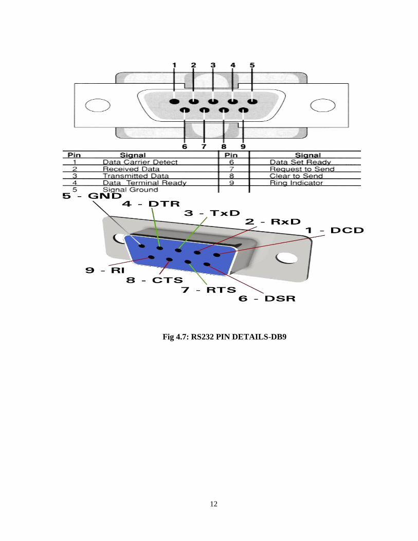
12
Fig 4.7: RS232 PIN DETAILS-DB9

13
A RS232 connection transmits signals using a positive voltage for a binary 0 and a negative
voltage for a binary 1. But what do the PLCs use RS232 for?
PLCs use RS232 to talk to other modules or even other PLCs. These modules can be anything that
also uses RS232 such as, operator interface or HMI, computers, motor controllers or drives, a
robot, or some kind of vision system.
DTE stands for Data Terminal Equipment. A common example of this is a computer.
DCE stands for Data Communications Equipment. An example of DCE is a modem.
The reason this is important is because two DTE or two DCE devices cannot talk to each other
without some help. This is typically done by using a reverse (null-modem) RS232 cable
connection to connect the devices.
Typically our PLCs will be DTE and our devices used will be DCE and everything should talk to
each other.
One very common example that many people are probably familiar with is a computer connected
to a printer. While USB has become the standard, RS232 is still widely used for older printers in
the workplace.
The RS232 protocol and cable allow the computer to give commands to the printer via a voltage
signal. The printer then deciphers those commands and completes the print.
One is the speed at which data can be transferred. Data can be transferred at around 20 kilobytes
per second. That is pretty slow compared to what people are used to now.
Another issue with RS232 is that the maximum length a cable is about 50 feet. Wire resistance and
voltage drops become an issue with cables longer than this. This is one reason RS232 is not used
as much as newer technology for remote installations.
Fig 4.8: DTE & DCE Connection using RS232

14
Fig 4.9: RS232 PIN DETAILS-DB 25

15
Fig 4.10: RS232 Line Driver

16
Fig 4.11: RS232 Connection
RS232 bit streams
The RS232 standard describes a communication method where information is sent bit by bit on a
physical channel. The information must be broken up in data words. The length of a data word is
variable. On PC‗s a length between 5 and 8 bits can be selected. This length is the net information
length of each word. For proper transfer additional bits are added for synchronization and error
checking purposes. It is important, that the transmitter and receiver use the same number of bits.
Otherwise, the data word may be misinterpreted, or not recognized at all.
With synchronous communication, a clock or trigger signal must be present which indicates the
beginning of each transfer. The absence of a clock signal makes an asynchronous communication
channel cheaper to operate. Less lines are necessary in the cable. A disadvantage is, that the
receiver can start at the wrong moment receiving the information. Re-synchronization is then
needed which costs time. All data received in the re-synchronization period is lost. Another
disadvantage is that extra bits are needed in the data stream to indicate the start and end of useful
information. These extra bits take up bandwidth.
Data bits are sent with a predefined frequency, the baud rate. Both the transmitter and receiver
must be programmed to use the same bit frequency. After the first bit is received, the receiver
calculates at which moments the other data bits will be received. It will check the line voltage
levels at those moments.
With RS232, the line voltage level can have two states. The on state is also known as mark, the off
state as space. No other line states are possible. When the line is idle, it is kept in the mark state.
Start bit
RS232 defines an asynchronous type of communication. This means, that sending of a data word
can start on each moment. If starting at each moment is possible, this can pose some problems for
the receiver to know which is the first bit to receive. To overcome this problem, each data word is
started with an attention bit. This attention bit, also known as the start bit, is always identified by
the space line level. Because the line is in mark state when idle, the start bit is easily recognized by
the receiver.
Data bits
Directly following the start bit, the data bits are sent. A bit value 1 causes the line to go in mark
state, the bit value 0 is represented by a space. The least significant bit is always the first bit sent.

17
Parity bit
For error detecting purposes, it is possible to add an extra bit to the data word automatically. The
transmitter calculates the value of the bit depending on the information sent. The receiver performs
the same calculation and checks if the actual parity bit value corresponds to the calculated value.
This is further discussed in another paragraph.
Stop bits
Suppose that the receiver has missed the start bit because of noise on the transmission line. It
started on the first following data bit with a space value. This causes garbled date to reach the
receiver. A mechanism must be present to re-synchronize the communication. To do this, framing
is introduced. Framing means, that all the data bits and parity bit are contained in a frame of start
and stop bits. The period of time lying between the start and stop bits is a constant defined by the
baud rate and number of data and parity bits. The start bit has always space value, the stop bit
always mark value. If the receiver detects a value other than mark when the stop bit should be
present on the line, it knows that there is a synchronization failure. This causes a framing error
condition in the receiving UART. The device then tries to re-synchronize on new incoming bits.
RS232 physical properties
The RS232 standard describes a communication method capable of communicating in different
environments. This has had its impact on the maximum allowable voltages etc. on the pins. In the
original definition, the technical possibilities of that time were taken into account. The maximum
baud rate defined for example is 20 kbps. With current devices like the 16550A UART, maximum
speeds of 1.5 Mbps are allowed.
Voltages
The signal level of the RS232 pins can have two states. A high bit, or mark state is identified by a
negative voltage and a low bit or space state uses a positive value. This might be a bit confusing,
because in normal circumstances, high logical values are defined by high voltages also.
Maximum cable lengths
Cable length is one of the most discussed items in RS232 world. The standard has a clear answer,
the maximum cable length is 50 feet, or the cable length equal to a capacitance of 2500 pF. The
latter rule is often forgotten. This means that using a cable with low capacitance allows you to span
longer distances without going beyond the limitations of the standard. If for example UTP CAT-5
cable is used with a typical capacitance of 17 pF/ft, the maximum allowed cable length is 147 feet.

18
RS485
Fig 4.12: RS485 Line Driver

19
Fig 4.13: complex RS485 network
Table 4.1:Comparison of RS232 vs RS485
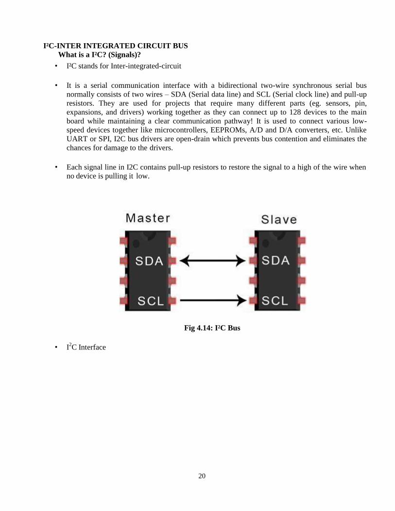
20
I²C-INTER INTEGRATED CIRCUIT BUS
What is a I²C? (Signals)?
• I²C stands for Inter-integrated-circuit
• It is a serial communication interface with a bidirectional two-wire synchronous serial bus
normally consists of two wires – SDA (Serial data line) and SCL (Serial clock line) and pull-up
resistors. They are used for projects that require many different parts (eg. sensors, pin,
expansions, and drivers) working together as they can connect up to 128 devices to the main
board while maintaining a clear communication pathway! It is used to connect various low-
speed devices together like microcontrollers, EEPROMs, A/D and D/A converters, etc. Unlike
UART or SPI, I2C bus drivers are open-drain which prevents bus contention and eliminates the
chances for damage to the drivers.
• Each signal line in I2C contains pull-up resistors to restore the signal to a high of the wire when
no device is pulling it low.
Fig 4.14: I²C Bus
• I2C Interface

21
• I2C uses only two wires: SCL (serial clock) and SDA (serial data).
• Both need to be pulled up with a resistor to +Vdd. There are also I2C level shifters which can be
used to connect to two I2C buses with different voltages.
• I
2C Addresses
• Basic I
2C communication is using transfers of 8 bits or bytes.
• Each I
2C slave device has a 7-bit address that needs to be unique on the bus.
• Some devices have fixed I
2C address while others have few address lines which determine
lower bits of the I2C address.
• This makes it very easy to have all I
2C devices on the bus with unique I
2C address. There are
also devices which have 10-bit address as allowed by the specification.
• 7-bit address represents bits 7 to 1 while bit 0 is used to signal reading from or writing to the
device. If bit 0 (in the address byte) is set to 1 then the master device will read from the slave
I2C device.
• Master device needs no address since it generates the clock (via SCL) and addresses individual
I2C slave devices Each signal line in I
2C contains pull-up resistors to restore the signal to a high
of the wire when no device is pulling it low
Fig 4.15: I²C Bus_Master & Slave
In normal state both lines (SCL and SDA) are high. The communication is initiated by the master
device. It generates the Start condition (S) followed by the address of the slave device (B1). If the
bit 0 of the address byte was set to 0 the master device will write to the slave device (B2).
Otherwise, the next byte will be read from the slave device. Once all bytes are read or written (Bn)

22
the master device generates Stop condition (P). This signals to other devices on the bus that the
communication has ended and another device may use the bus.
Most I
2C devices support repeated start condition. This means that before the communication ends
with a stop condition, master device can repeat start condition with address byte and change the
mode from writing to reading.
I2C bus is used by many integrated circuits and is simple to implement. Any microcontroller can
communicate with I2C devices even if it has no special I
2C interface. I
2C specifications are
flexlible – I2C bus can communicate with slow devices and can also use high speed modes to
transfer large amounts of data. Because of many advantages, I2C bus will remain as one of the
most popular serial interfaces to connect integrated circuits on the board.
Fig 4.16: Master device writes data to slave device
I²C communication protocol
I2C data is transferred in messages which are broken up into data frames.
Each message contains:
Start condition
Address of the Slave
Read and write bits
Data frame
ACK/NACK bits
Stop condition
Start Condition:
The transmission will start when the master device switches the SDA line from high voltage level to low voltage level then switches the SCL line from high to low.
Signals to other slave device that a transmission is going to happen.

23
If two masters sends a start condition at one time wants to take ownership of the bus,
whoever pulls the SDA low first ―wins‖
Stop Condition:
A stop condition will be transmitted after all the data frames have been sent.
The SCL line will switch from a low voltage level to high first before the SDA line switches from a low voltage to high
Value on SDA should not change when SCL is high during normal data writing operation as
it can cause false stop conditions.
Read/Write Bit
Single bit specifying whether the master is transmitting (write) data to the slave (low voltage
level) or requesting (read) data from it (high voltage level).
ACK/NACK Bit
Sent by the the receiving device after each frame to signal to the sender whether the data frame was
successfully received (ACK) or not (NACK)
Fig 4.17:I²C communication protocol
Addressing
Compared to SPI, I2C do not have slave select lines which causes the slave devices not being able know when data is being sent to him instead of other slave.
To solve this problem, I2C uses an address frame which is the first frame after the start bit in a new
message.

24
Master devices will first send the unique address of the slave it wants to communicate with. I
If the address does matches with the slave own address, it will send a ACK bit back to the master
device.
If it does not match, the slave will do nothing which leaves the SDA line high.
Data Frame (data to be transmitted)
After the address frame has been sent and master device receives a ACK bit from the slave, data
will begin being transmitted which are 8 bits long with the most significant bits (MSB) being sent
first.
While the master device will be generating clock pulses at regular intervals, data are sent on the
SDA by the master or the slave depending on the Read/write bit.
After this process have been completed, the master will send a stop condition to the slave which
will end the transmission.
Step by step of I2C communication
Firstly, a start signal will be generated by the master device which signals to the other devices to
start listening to the bus and prepare to receive data. (SCL high, SDA switch from high to low)
When a start signal condition is transmitted, the bus will enter a busy state where the current data
transfer is limited to only the selected master and slave. It is only after a stop condition is generated
where the bus will be released and be in an idle mode again.
Secondly, the master device will send a 7-bit device address plus one bit of reading and write the
data frame to every device. The bit will also indicate the direction of the next data transmission. 0 =
Master device writes data to the slave devices. 1 = Master device reads data to the slave devices.
Thirdly, Each slave compares the address sent by the master with its own address. The slave device that successfully matches the address returns the ACK bit by pulling the SDA line low.
Fourthly, when the master device receives an acknowledgment signal from the slave device, it will
start transmitting or receiving data
Fifthly, after transmitting each data frame, the receiving device returns another ACK bit to the
sender to confirm that the frame is successfully received, and then the sender continues to transmit
the data frame, and so on.
Lastly, when the data transfer is completed, the master device will send a stop signal which signals
the release of the bus to other devices and the bus will enter an idle state.

25
Fig 4.18:I²C communication protocol message
SPI- Serial Peripheral Interface (SPI)
A serial peripheral interface (SPI) is an interface that enables the serial (one bit at a time)
exchange of data between two devices, one called a master and the other called a slave .
It provides serial exchange of data between two devices(Master,Slave)
Moving data simply and quickly from one device to another
Features
Master/Slave -Supports up to 15 external devices Supports SPI modes 0, 1, 2 & 3
8 to 16 bit Data Length
Primarily intended for on-board communication.
Flexible clock format.
Full Duplexed operation.
MSB or LSB first.
Communication may be interrupt driven.
Fixed or Variable peripheral selection
Bi-directional data exchange
The Serial Peripheral Interface (SPI) is a synchronous serial communication interface specification used for short-distance communication, primarily in embedded systems.
The interface was developed by Motorola in the mid-1980s
Typical applications include Secure Digital cards and liquid crystal displays.

26
SPI devices communicate in full duplex mode using a master-slave architecture with a single master.
The master device originates the frame for reading and writing. Multiple slave-devices are supported through selection with individual slave select (SS), sometimes called chipselect
(CS), lines.
Fig 4.18:I²C communication protocol message
Fig 4.19: SPI communication
The SPI bus specifies four logic signals:
SCLK: Serial Clock (output from master)
MOSI: Master Out Slave In (data output from master)
MISO: Master In Slave Out (data output from slave)
SS: Slave Select (often active low, output from master)
MOSI on a master connects to MOSI on a slave. MISO on a master connects to MISO on a slave.
Slave Select has the same functionality as chip select and is used instead of an addressing concept.
Note: on a slave-only device, MOSI may be labeled as SDI (Slave Data In) and MISO may be
labeled as SDO (Slave Data Out)
The signal names above can be used to label both the master and slave device pins as well as the
signal lines between them in an unambiguous way, and are the most common in modern products.

27
Pin names are always capitalized e.g. "Slave Select," not "slave select."
Older products can have nonstandard SPI pin names:
Serial Clock: SCK
Fig 4.20: SPI Data Transmission

28
SPI Data Loop
Fig 4.21: SPI Data Loop
SSPSR- Synchronous serial port shift register
Internal Shift Register , Loaded by SPI data or from SSPBUF
SSPBUF-Synchronous serial port buffer
Serial Buffer This is the register read and written by your program
SCK- Serial Clock
Master generates the clock the controls the data transfer
SS-Slave Select
Master controls which slave is selected by asserting the slave‗s SS
Applications
SPI is used to talk to a variety of peripherals, such as
Sensors: temperature, pressure, ADC, touchscreens, video game controllers
Control devices: audio codecs, digital potentiometers, DAC
Camera lenses: Canon EF lens mount
Communications: Ethernet, USB, USART, CAN, IEEE 802.15.4, IEEE 802.11, handheld
video games
Memory: flash and EEPROM
Real-time clocks

29
LCD displays, sometimes even for managing image data
Any MMC or SD card (including SDIO variant)
Advantages
Full duplex communication
Higher throughput than I²C or SMBus
Complete protocol flexibility for the bits transferred
Not limited to 8-bit words
Arbitrary choice of message size, content, and purpose
Extremely simple hardware interfacing
Typically lower power requirements than I²C or SMBus due to less circuitry (including pullups)
No arbitration or associated failure modes
Slaves use the master's clock, and don't need precision oscillators
Slaves don't need a unique address — unlike I²C or GPIB or SCSI
Transceivers are not needed
Uses only four pins on IC packages, and wires in board layouts or connectors, much less than parallel interfaces
At most one unique bus signal per device (chip select); all others are shared
Signals are unidirectional allowing for easy Galvanic isolation
Disadvantages
Requires more pins on IC packages than I²C, even in the 3-wire variant
No in-band addressing; out-of-band chip select signals are required on shared buses
No hardware flow control by the slave (but the master can delay the next clock edge to slow the
transfer rate)
No hardware slave acknowledgment (the master could be transmitting to nowhere and not know it)
Supports only one master device
No error-checking protocol is defined
Generally prone to noise spikes causing faulty communication,
Without a formal standard, validating conformance is not possible
Only handles short distances compared to RS-232, RS-485, or CAN-bus
Many existing variations, making it difficult to find development tools like host adapters that support those variations
Fig 4.22: Comparison of Communication protocol

30
Table 4.2: Comparison of Communication protocol
Table 4.3: Comparison of SPI and I2C protocol
UNIVERSAL SERIAL BUS:
an external serial bus interface standard for connecting peripheral devices to a computer, as ina
USB port or USB cable.
The most widely used hardware interface for attaching peripherals to a computer. There are
typically at least two USB ports on laptops and four on desktop computers, while USB "hubs"
allow many more connections (see below). After appearing on PCs in 1997, USB quicklybecame
popular for connecting keyboards, mouse, printers and hard drives, eventually replacing the PC's
serial and parallel ports.
A serial bus standard for connecting devices usually peripheral devices to computers.
31
Features
Single connector type
Replaces all different legacy connectors with one well-defined standardized USB connector for all USB peripheral devices
Hot swappable
Devices can be safely plugged and unplugged as needed while the computer is running (no
need to reboot)
Plug and Play
OS software automatically identifies, configures, and loads the appropriate driver when connection is made
High performance
USB offers data transfer speeds at up to 480 Mbps
Expandability
Up to 127 different peripheral devices may theoretically be connected to a single bus at one time
Bus-supplied power
USB distributes the power to all connected devices, eliminating the need for anexternal
power source for low power devices (flash drives, memory cards, Bluetooth)
Easy to use
The single standard connector type simplifies the end user‗s task of figuring out what plug goes into what socket
Automatic driver loading does all the work for the end user
Low cost
The host handles most of the protocol complexity, making the design simple and having a low cost
Versions
There have been three versions released prior to 3.0
⚫ USB 1.0 in January 1996 – data rates of 1.5 Mbps and 12 Mbps
⚫ USB 1.1 in September 1998 – first widely used version of USB
⚫ USB 2.0 in April 2000
⚫ Major feature revision was the addition of a high speed transfer rate of 480 Mbps
⚫ Important note – all versions are backwards compatible with previous versions of USB
USB 1.0, 2.0 and 3.0
Supporting up to 127 devices, USB 1.0 (1996) and USB 1.1 (1998) provide a Low-Speed 1.5 Mbps subchannel for keyboards and mice and a Full-Speed channel at 12 Mbps.
Hi-Speed USB 2.0 (2001) jumps the top rate to 480 Mbps, while SuperSpeed USB 3.0 (2008)
provides a huge 10x increase to 4.8 Gbps (see USB 3.0).
The USB cable provides four pathways- two power conductors and two twisted signal conductors.

32
The USB device that uses full speed bandwidth devices must have a twisted pair D+ and D-
conductors. The data is transferred through the D+ and D- connectors while Vbus and Gnd
connectors provide power to the USB device.
Architecture of a USB network
Consists of one host device and multiple daisy chained devices
Fig 4.23: Architecture of a USB network
Two kinds of Hubs:
• Bus Powered Hub: Draws power from the host computers USB interface
• Self Powered Hub: Has a built in power supply.

33
Fig 4.24: USB TOPOLOGY
Tier One drives are built from the highest quality memory chips and are recognized as the most
dependable form of USB Flash Drives on the market.

34
Fig 4.25: USB TYPE A

35
Fig 4.26: USB TYPE B
Fig 4.27: USB MINI A& B

36
Fig 4.28: MICRO USB
• Mini-USB. As the name suggests, this is a smaller connection type that's good for mobile
devices. ...
• Micro-USB.
•

37
Fig 4.29:TOKEN PACKETS
Fig 4.30: FIELD OF USB

38
Fig 4.31: FIELD OF USB
There are some important advantages of universal serial bus (USB) are given below,
• The universal serial bus is easy to use.
• It has robust connector system.
• It has low cost.
• It has variety of connector types and size available.
• It has true plug and play nature.
• It has Low power consumption.
• Daisy chain up to 127 USB components / peripherals at the same time to one PC.
• Fits almost all devices that have a USB port.
There are some important disadvantages of universal serial bus (USB) are given below,
• It has limited capability and overall performance.
• Universal Serial Bus does not provide the broadcasting feature, only individual messages can be
communicated between host and peripheral.
• The data transfer not as fast as some other systems.
• What is CAN bus?
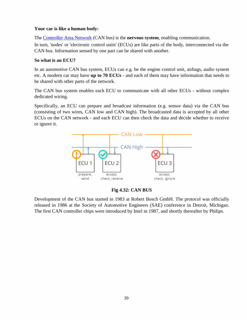
39
Your car is like a human body:
The Controller Area Network (CAN bus) is the nervous system, enabling communication.
In turn, 'nodes' or 'electronic control units' (ECUs) are like parts of the body, interconnected via the
CAN bus. Information sensed by one part can be shared with another.
So what is an ECU?
In an automotive CAN bus system, ECUs can e.g. be the engine control unit, airbags, audio system
etc. A modern car may have up to 70 ECUs - and each of them may have information that needs to
be shared with other parts of the network.
The CAN bus system enables each ECU to communicate with all other ECUs - without complex
dedicated wiring.
Specifically, an ECU can prepare and broadcast information (e.g. sensor data) via the CAN bus
(consisting of two wires, CAN low and CAN high). The broadcasted data is accepted by all other
ECUs on the CAN network - and each ECU can then check the data and decide whether to receive
or ignore it.
Fig 4.32: CAN BUS
Development of the CAN bus started in 1983 at Robert Bosch GmbH. The protocol was officially
released in 1986 at the Society of Automotive Engineers (SAE) conference in Detroit, Michigan.
The first CAN controller chips were introduced by Intel in 1987, and shortly thereafter by Philips.

40
Fig 4.33: CAN BUS CONTROLLER
CAN Applications
• Passenger cars
• Trucks and buses
• Off-highway and off-road vehicles
• Passenger and cargo trains
• Maritime electronics
• Aircraft and aerospace electronics
• Factory automation
• Industrial machine control

41
• Lifts and escalators
• Building automation
• Medical equipment and devices
• Non-industrial control
• Non-industrial equipment
CAN ADVANTAGES
• Simple & low cost
• ECUs communicate via a single CAN system instead of via direct complex analoguesignal
lines - reducing errors, weight, wiring and costs
• Fully centralized
• The CAN bus provides 'one point-of-entry' to communicate with all network ECUs - enabling
central diagnostics, data logging and configuration
• Extremely robust
• The system is robust towards electric disturbances and electromagnetic interference - ideal for
safety critical applications (e.g. vehicles)
• Efficient
• CAN frames are prioritized by ID so that top priority data gets immediate bus access, without
causing interruption of other frames
CAN IMPLEMENTATION
Fig 4.34: STAND ALONE CAN BUS
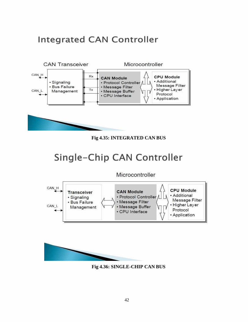
42
Fig 4.35: INTEGRATED CAN BUS
Fig 4.36: SINGLE-CHIP CAN BUS
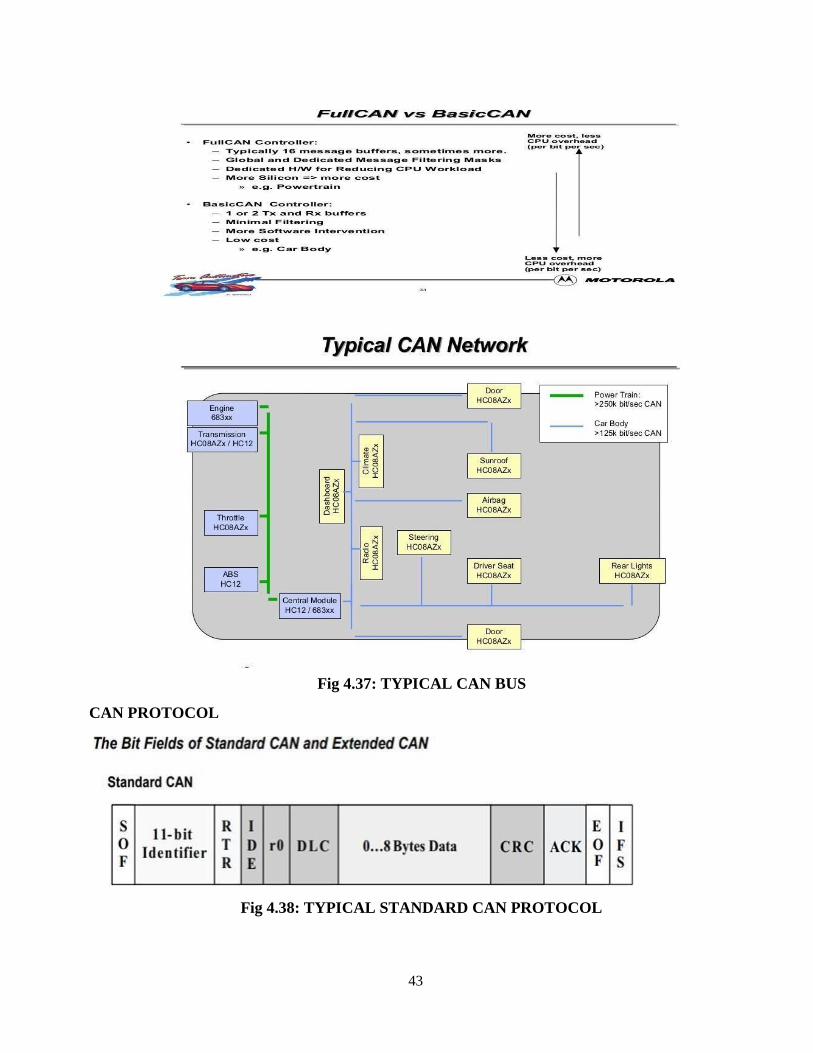
43
Fig 4.37: TYPICAL CAN BUS
CAN PROTOCOL
Fig 4.38: TYPICAL STANDARD CAN PROTOCOL

44
Fig 4.38: TYPICAL EXTENDED CAN PROTOCOL
SOF–The single dominant start of frame (SOF) RTR–
The single remote transmission request (RTR) IDE–A
dominant single identifier extension (IDE)
• DLC–The 4-bit data length code (DLC)
CRC–The 16-bit (15 bits plus delimiter) cyclic redundancy check (CRC)
acknowledges (ACK)
EOF–This end-of-frame (EOF), IFS–
This 7-bit interframe space (IFS) The
meaning of the bit fields are:
• SOF–The single dominant start of frame (SOF) bit marks the start of a message, and is used to synchronize the nodes on a bus after being idle.
• Identifier-The Standard CAN 11-bit identifier establishes the priority of the message. The lower the binary value, the higher its priority.
• RTR–The single remote transmission request (RTR) bit is dominant when information is required
from another node. All nodes receive the request, but the identifier determines the specified node. The
responding data is also received by all nodes and used by any node interested. In this way, all data
being used in a system is uniform.
• IDE–A dominant single identifier extension (IDE) bit means that a standard CAN identifier with no extension is being transmitted. • r0–Reserved bit (for possible use by future standard amendment).
• DLC–The 4-bit data length code (DLC) contains the number of bytes of data being transmitted.
• Data–Up to 64 bits of application data may be transmitted.
• CRC–The 16-bit (15 bits plus delimiter) cyclic redundancy check (CRC) contains the checksum
(number of bits transmitted) of the preceding application data for error detection.
• ACK–Every node receiving an accurate message overwrites this recessive bit in the original message
with a dominate bit, indicating an error-free message has been sent. Should a receiving node detect an
error and leave this bit recessive, it discards the message and the sending node repeats the message after
rearbitration. In this way, each node acknowledges (ACK) the integrity of its data. ACK is 2 bits, one is

45
the acknowledgment bit and the second is a delimiter.
• EOF–This end-of-frame (EOF), 7-bit field marks the end of a CAN frame (message) and disables
bitstuffing, indicating a stuffing error when dominant. When 5 bits of the same logic level occur in
succession during normal operation, a bit of the opposite logic level is stuffed into the data.
• IFS–This 7-bit interframe space (IFS) contains the time required by the controller to move a correctly
received frame to its proper position in a message buffer area.
• SRR–The substitute remote request (SRR) bit replaces the RTR bit in the standard message location
as a placeholder in the extended format.
• IDE–A recessive bit in the identifier extension (IDE) indicates that more identifier bits follow. The
18-bit extension follows IDE.
• r1–Following the RTR and r0 bits, an additional reserve bit has been included ahead of the DLC bit
CAN Message Frame
Four types of frames.
Data frame.Transmits information.
Remote frame.Request information
Error frame.Indicates occurance of error.
Overload frame.Indicates more time required to process message.
Message Types
The Data Frame - The data frame is the most common message type, and comprises the Arbitration
Field, the Data Field, the CRC Field, and the Acknowledgment Field. The Arbitration Field contains an
11-bit identifier in Figure 2 and the RTR bit, which is dominant for data frames. In Figure 3, it contains
the 29-bit identifier and the RTR bit. Next is the Data Field which contains zero to eight bytes of data,
and the CRC Field which contains the 16-bit checksum used for error detection. Last is the
Acknowledgment Field.
The Remote Frame : The intended purpose of the remote frame is to solicit the transmission of data
from another node. The remote frame is similar to the data frame, with two important differences. First,
this type of message is explicitly marked as a remote frame by a recessive RTR bit in the arbitration
field, and secondly, there is no data.
The Error Frame The error frame is a special message that violates the formatting rules of a CAN
message. It is transmitted when a node detects an error in a message, and causes all other nodes in the
network to send an error frame as well. The original transmitter then automatically retransmits the
message. An elaborate system of error counters in the CAN controller ensures that a node cannot tie up
a bus by repeatedly transmitting error frames.
The Overload Frame The overload frame is mentioned for completeness. It is similar to the error
frame with regard to the format, and it is transmitted by a node that becomes too busy. It is primarily
used to provide for an extra delay between messages. A Valid Frame A message is considered to be
error free when the last bit of the ending EOF field of a message is received in the error-free recessive
state. A dominant bit in the EOF field causes the transmitter to repeat a transmission.

46
Fig 4.39: BUS ARTIBRATION
Ethernet is a way of connecting computers together in a local area network or LAN. It has been the
most widely used method of linking computers together in LANs since the 1990s. The basic idea of its
design is that multiple computers have access to it and can send data at any time
The difference between internet and ethernet is that the internet is a wide area network (WAN)
while the ethernet is a local area network (LAN). Internet is a worldwide large network that connects
a large number of devices around the world while ethernet is a network that covers a small
geographical area.
Ethernet is the traditional technology for connecting devices in a wired local area network (LAN) or
wide area network (WAN), enabling them to communicate with each other via a protocol -- a set of
rules or common network language. ... An Ethernet cable is the physical, encased wiring over which
the data travels.

47
Fig 4.40: ETHERNET CABLE
Features
It is a broadcast protocol
Most popular packet switched LAN technology

48
• It uses a Bus or Star topology.
• Supports data transfer rates of upto 10 Mbps.
• Bandwidths: 10Mbps, 100Mbps, 1Gbps
• Max bus length: 2500m
– 500m segments with 4 repeaters
• Bus and Star topologies are used to connect hosts
– Hosts attach to network via Ethernet transceiver or hub or switch
• Detects line state and sends/receives signals
– Hubs are used to facilitate shared connections
– All hosts on an Ethernet are competing for access to the medium
• Switches break this model
• Problem: Distributed algorithm that provides fair access
• Preamble is a sequence of 7 bytes, each set to ―10101010‖
– Used to synchronize receiver before actual data is sent
• Addresses
– unique, 48-bit unicast address assigned to each adapter
• example: 8:0:e4:b1:2
• Each manufacturer gets their own address range
– broadcast: all 1s
– multicast: first bit is 1
• Type field is a demultiplexing key used to determine which higher level protocol the frame
should be delivered to
• Body can contain up to 1500 bytes of data
Fig 4.41: ETHERNET MESSAGE FRAME
LAN standards
It defines MAC and physical layer connectivity :
-IEEE 802.3 (CSMA/CD - Ethernet) standard – originally 2Mbps
-IEEE 802.3u standard for 100Mbps Ethernet
-IEEE 802.3z standard for 1,000Mbps Ethernet
CSMA/CD:
Ethernet‗s Media Access Control (MAC) policy
CS = carrier sense.(Send only if medium is idle)
MA = multiple access.
CD = collision detection.
(Stop sending immediately if collision is detected)
Ethernet‗s MAC Algorithm
• In Aloha, decisions to transmit are made without paying attention to what other nodes might be
doing
• Ethernet uses CSMA/CD – listens to line before/during sending • If line is idle (no carrier sensed)
– send packet immediately

49
– upper bound message size of 1500 bytes
– must wait 9.6us between back-to-back frames
• If line is busy (carrier sensed)
– wait until idle and transmit packet immediately
• called 1-persistent sending
• If collision detected
– Stop sending and jam signal – Try again later
Ethernet – IEEE 802.3
• 10Base5 – Thick wire coaxial
• 10Base2 – thin wire coaxial / cheaper net
• 10BaseT – Twisted Pair
• 10BaseF – Fiber Optics
100BaseT – Fast Ethernet
Ethernet Technologies
Fig 4.41: ETHERNET TECHNOLOGIES
Ethernet Devices
Repeater – Restores data and collision signals
Bridge - Connecting two or more collision domains
Router - Network layer device
Switch – Multiport bridge with parallel paths
Advantages
Ethernets work best under light loads
Utilization over 30% is considered heavy
- Network capacity is wasted by collisions

50
Most networks are limited to about 200 hosts
Specification allows for up to 1024 bits
Ethernet is inexpensive, fast and easy to maintenance.
Disadvantages
Ethernet‗s peak utilization is low .
Peak output is worst with more hosts.
More collisions needed to identify single sender due to Smaller packet size
Collisions take longer to observe, more bandwidth is wasted
Applications
Digital Camcorders and VCRs
Direct-to-Home (DTH) satellite audio/video
Cable TV and MMDS (microwave) set-top boxes
DVD Players
Video Games
Home Theater
TEXT / REFERENCE BOOKS
1. Kenneth. J. Ayala, ―The 8051 Microcontroller Architecture, Programming and Apllications‖, Penram
International, 1996, 2 nd Edition.
2. Sriram. V. Iyer, Pankaj Gupta, ―Embedded Real Time Systems Programming‖, 2004 Tata McGraw Hill
Publishing Company Limited, 2006.
3. Frank Vahid, Tony Givargis, ‗Embedded system Design - A unified Hardware / software Introduction‘,
John Wiley and Sons, 2002.
4. Todd D Morton, ‗Embedded Microcontrollers‘, Reprint by 2005, Low Price Edition. 5. Muhammed Ali Mazidi, Janice Gillispie Mazidi, ‗The 8051 Microcontroller and Embedded Systems‘,
Low Price Edition, Second Impression 2006.
6. Raj Kamal, ‗Embedded Systems-Architecture, Programming and Design‘, Tata McGraw Hill
Publishing Company Limited 2003.
7. Muhammed Ali Mazidi, Rolin D.Mckinlay, Dannycauscy, ―PIC microcontrollers and embedded
systems using assembly and C‖, 1st edition, Pearson, 2007.

1
SCHOOL OF ELECTRICAL AND ELECTRONICS
DEPARTMENT OF ELECTRICAL AND ELECTRONICS ENGINEERING
PRINCIPLES OF EMBEDDED SYSTEM DESIGN-SECA1706

2
UNIT-V
REAL TIME OPERATING SYSTEMS

3
V. UNIT – V
REAL TIME OPERATING SYSTEMS
SYLLABUS:
Introduction - Desktop OS versus RTOs - Task management - Task scheduling - Race
conditions - Priority Inversion - ISRs and Scheduling - Intertask Communication.
A Real-Time Operating System (RTOS) comprises of two components, viz., ―Real-Time‖ and
―Operating System‖.
An Operating system (OS) is nothing but a collection of system calls or functions which provides an
interface between hardware and application programs. It manages the hardware resources of a computer
and hosting applications that run on the computer. An OS typically provides multitasking,
synchronization, Interrupt and Event Handling, Input/ Output, Inter-task Communication, Timers and
Clocks and Memory Management. Core of the OS is the Kernel which is typically a small, highly
optimised set of libraries.
Real-time systems are those systems in which the correctness of the system depends not only on
the logical result of computation, but also on the time at which the results are produced.
RTOS is therefore an operating system that supports real-time applications by providing logically
correct result within the deadline required. Basic Structure is similar to regular OS but, in addition, it
provides mechanisms to allow real time scheduling of tasks.
Though real-time operating systems may or may not increase the speed of execution, they can provide much more precise and predictable timing characteristics than general-purpose OS.
RTOS is key to many embedded systems and provides a platform to build applications. All embedded
systems are not designed with RTOS. Embedded systems with relatively simple/small hardware/code
might not require an RTOS. Embedded systems with moderate-to-large software applications require
some form of scheduling, and hence RTOS.
Advantages of a real-time operating system
An RTOS provides a variety of business benefits, including:
Optimizes the system: the RTOS gives an indication of all activities taking place within the system to
ensure that all departments or sections are active. This maximizes production or operations, making
them more reliable.
Links systems: the small size and little interaction involved enables operators to connect systems or
departments, making them easier to monitor and manage.
Shows activeness of processes and procedures: the focus is on what is happening in real time. As such,
it is easier to monitor events, production, activity, etc. Inactive areas can be spotted within a short time
for faster correction or intervention.
Reduces error: the fact that real-time operating systems operate in real time reduces the chances of
error. Any mishap can be corrected quickly.
Tracks efficiently: an RTOS has a memory slot that makes it easier to track changes or activities in
different sections.

4
RTOS CLASSFICATION
RTOS specifies a known maximum time for each of the operations that it performs. Based upon the
degree of tolerance in meeting deadlines, RTOS are classified into following categories
· Hard real-time: Degree of tolerance for missed deadlines is negligible. A missed deadline can
result in catastrophic failure of the system
· Firm real-time: Missing a deadly ne might result in an unacceptable quality reduction but may
not lead to failure of the complete system
· Soft real-time: Deadlines may be missed occasionally, but system doesn‗t fail and also, system quality is acceptable
For a life saving device, automatic parachute opening device for skydivers, delay can be fatal.
Parachute opening device deploys the parachute at a specific altitude based on various conditions. If it
fails to respond in specified time, parachute may not get deployed at all leading to casualty. Similar
situation exists during inflation of air bags, used in cars, at the time of accident. If airbags don‗t get
inflated at appropriate time, it may be fatal for a driver. So such systems must be hard real time
systems, whereas for TV live broadcast, delay can be acceptable. In such cases, soft real time systems
can be used.
Soft real-time
Tasks are performed as fast as possible
Late completion of jobs is undesirable but not fatal.
System performance degrades as more & more jobs miss deadlines
Example: Online Databases
Hard real-time
Tasks have to be performed on time
Failure to meet deadlines is fatal
Example : Flight Control System
Qualitative Definition
Important terminologies used in context of real time systems
Determinism: An application is referred to as deterministic if its timing can be guaranteed within a
certain margin of error.
Jitter: Timing error of a task over subsequent iterations of a program or loop is referred to as jitter. RTOS are optimized to minimize jitter.
RTOS Architecture – Kernel
RTOS Architecture
For simpler applications, RTOS is usually a kernel but as complexity increases, various modules like networking protocol stacks debugging facilities, device I/Os are includes in addition to the kernel.
The general architecture of RTOS is shown in the fig.

5
Fig 5.1: Architecture of RTOS
Kernel
RTOS kernel acts as an abstraction layer between the hardware and the applications. There are three broad categories of kernels
· Monolithic kernel
Monolithic kernels are part of Unix-like operating systems like Linux, FreeBSD etc. A monolithic
kernel is one single program that contains all of the code necessary to perform every kernel related task.
It runs all basic system services (i.e. process and memory management, interrupt handling and I/O
communication, file system, etc) and provides powerful abstractions of the underlying hardware.
Amount of context switches and messaging involved are greatly reduced which makes it run faster than
microkernel.
· Microkernel
It runs only basic process communication (messaging) and I/O control. It normally provides only the
minimal services such as managing memory protection, Inter process communication and the process
management. The other functions such as running the hardware processes are not handled directly by
microkernels. Thus, micro kernels provide a smaller set of simple hardware abstractions. It is more
stable than monolithic as the kernel is unaffected even if the servers failed (i.e.File
System). Microkernels are part of the operating systems like AIX, BeOS, Mach, Mac OS X, MINIX,
and QNX. Etc
· Hybrid Kernel

6
Hybrid kernels are extensions of microkernels with some properties of monolithic kernels. Hybrid
kernels are similar to microkernels, except that they include additional code in kernel space so that such
code can run more swiftly than it would were it in user space. These are part of the operating systems
such as Microsoft Windows NT, 2000 and XP. DragonFly BSD, etc
· Exokernel
Exokernels provides efficient control over hardware. It runs only services protecting the resources (i.e.
tracking the ownership, guarding the usage, revoking access to resources, etc) by providing low-level
interface for library operating systems and leaving the management to the application.
Fig 5.2: Types of KERNEL
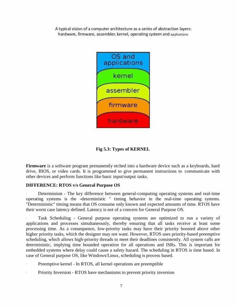
7
Fig 5.3: Types of KERNEL
Firmware is a software program permanently etched into a hardware device such as a keyboards, hard
drive, BIOS, or video cards. It is programmed to give permanent instructions to communicate with
other devices and perform functions like basic input/output tasks.
DIFFERENCE: RTOS v/s General Purpose OS
· Determinism - The key difference between general-computing operating systems and real-time
operating systems is the ―deterministic " timing behavior in the real-time operating systems.
"Deterministic" timing means that OS consume only known and expected amounts of time. RTOS have
their worst case latency defined. Latency is not of a concern for General Purpose OS.
· Task Scheduling - General purpose operating systems are optimized to run a variety of
applications and processes simultaneously, thereby ensuring that all tasks receive at least some
processing time. As a consequence, low-priority tasks may have their priority boosted above other
higher priority tasks, which the designer may not want. However, RTOS uses priority-based preemptive
scheduling, which allows high-priority threads to meet their deadlines consistently. All system calls are
deterministic, implying time bounded operation for all operations and ISRs. This is important for
embedded systems where delay could cause a safety hazard. The scheduling in RTOS is time based. In
case of General purpose OS, like Windows/Linux, scheduling is process based.
· Preemptive kernel - In RTOS, all kernel operations are preemptible
· Priority Inversion - RTOS have mechanisms to prevent priority inversion

8
· Usage - RTOS are typically used for embedded applications, while General Purpose OS are used
for Desktop PCs or other generally purpose PCs.
1. A regular OS focuses on computing throughput while an RTOS focuses on very fast response time
2. OSes are used in a wide variety of applications while RTOSes are generally embedded in devices
that require real time response
3. OSes use a time sharing design to allow for multi-tasking while RTOSes either use a time sharing
design or an even driven design
4. The coding of an RTOS is stricter compared to a standard OS
TABLE 5.1: COMPARE OS VS RTOS
9
Disadvantages of Real Time Operating System:-
There are some disadvantages of RTOS also. So every system has pros and cons so here are
some of bad things about RTOS.
Limited Tasks: – There are only limited tasks run at the same time and the concentration of
these system are on few application to avoid errors and other task have to wait. Sometime there
is no time limit of how much the waiting tasks have to wait.
Use heavy system resources: – RTOS used lot of system resources which is not as good and is
also expensive.
Low multi-tasking: – Multi tasking is done few of times and this is the main disadvantage of
RTOS because these system runs few tasks and stay focused on them. So it is not best for
systems which use lot of multi-threading because of poor thread priority.
Complex Algorithms: – RTOS uses complex algorithms to achieve a desired output and it is
very difficult to write that algorithms for a designer.
Device driver and interrupt signals: – RTOS must need specific device drivers and interrupt signals to response fast to interrupts.
Thread Priority: – Thread priority is not good as RTOS do less switching of tasks.
Expensive: – RTOS are usually very expensive because of the resources they need to work.
Not easy to program: – The designer have to write proficient program for real time operating system which is not easy as a piece of cake.
Low Priority Tasks: – The low priority tasks may not get time to run because these systems
have to keep accuracy of current running programs.
Precision of code: – Event handling of tasks is strict so more precision in code needed for
designer to program. Event must be responded quickly and this is not easy for exact precision
for the designer.
Other factors: – There are lot of factors needed to consider like memory management, CPU
and error handling.
In this tutorial article we have discussed advantages and disadvantages of Real time operating
systems. Some of these we have already discussed. There are some other detailed and complex
problems also which is not appropriate for this topic.
Architecture - Task Management
Task Management
· Task Object
In RTOS, The application is decomposed into small, schedulable, and sequential program units
known as ―Task‖, a basic unit of execution and is governed by three time-critical properties;
release time, deadline and execution time. Release time refers to the point in time from which
the task can be executed. Deadline is the point in time by which the task must complete.
Execution time denotes the time the task takes to execute.

10
Each task may exist in following states
· Dormant : Task doesn‗t require computer time
· Ready: Task is ready to go active state, waiting processor time
· Active: Task is running
· Suspended: Task put on hold temporarily
· Pending: Task waiting for resource.
Fig 5.3: TASK MANAGEMENT
During the execution of an application program, individual tasks are continuously changing
from one state to another. However, only one task is in the running mode (i.e. given CPU
control) at any point of the execution. In the process where CPU control is change from one task
to another, context of the to-be-suspended task will be saved while context of the to-be-executed
task will be retrieved, the process referred to as context switching.
A task object is defined by the following set of components:
· Task Control block: Task uses TCBs to remember its context. TCBs are data structures
residing in RAM, accessible only by RTOS
Task Stack: These reside in RAM, accessible by stack pointer.
· Task Routine: Program code residing in ROM
5.

11
TABLE 5.1 TASK CONTROL BLOCK
Task_ID
Task_State
Task_Priority
Task_Stack_Pointer
Task_Prog _Counter
Fig 5.3: TASK MANAGEMENT
Fig 5.4: TASK MANAGEMENT

12
Fig 5.5: TASK MANAGEMENT STATES
Fig 5.6: TASK MANAGEMENT STATES

13
EXAMPLE FOR TASK MANAGEMENT
Operating Systems
Allow the processor to perform several tasks at virtually the same time
Ex. Web Controlled Car with a camera
• Car is controlled via the internet
• Car has its own webserver (http://mycar/)
• Web interface allows user to control car and see camera images
• Car also has ―auto brake‖ feature to avoid collisions
Fig 5.4: Web interface view
Multiple Tasks
Assume that one microcontroller is being used
At least four different tasks must be performed
Send video data - This is continuous while a user is connected
Service motion buttons - Whenever button is pressed, may last seconds
Detect obstacles - This is continuous at all times
Auto brake - Whenever obstacle is detected, may last seconds
Detect and Auto brake cannot occur together
3 tasks may need to occur concurrently
Task Scheduling :
Scheduler
The scheduler keeps record of the state of each task and selects from among them that are ready
to execute and allocates the CPU to one of them. Various scheduling algorithms are used in
RTOS
Polled Loop: Sequentially determines if specific task requires time.

14
Fig 5.5: Polled loop
Polled System with interrupts. In addition to polling, it takes care of critical tasks.
Fig 5.6: Polled System with interrupts
Round Robin : Sequences from task to task, each task getting a slice of time
Fig 5.7: Round Robin
Hybrid System: Sensitive to sensitive interrupts, with Round Robin system working in
background
· Interrupt Driven: System continuously wait for the interrupts
· Non pre-emptive scheduling or Cooperative Multitasking: Highest priority task
executes for some time, then relinquishes control, re-enters ready state.

15
Fig 5.7: Non pre-emptive scheduling
Preemptive scheduling Priority multitasking: Current task is immediately suspended Control
is given to the task of the highest priority at all time.
Fig 5.8: Pre-emptive scheduling
Dispatcher
The dispatcher gives control of the CPU to the task selected by the scheduler by performing
context switching and changes the flow of execution.
Run to completion [RTC]
An RTC scheduler is very simple. Indeed, I have previously [and only slight inaccurately]
referred to one as a ―one line RTOS‖. The idea is that one task runs until it has completed its
work, then terminates. Then the next task runs similarly. And so forth until all the tasks have
run, when the sequence starts again.

16
Fig 5.9:RTC- Run to completion
The simplicity of this scheme is offset by the drawback that each task‗s allocation of time is
totally affected by all the others. The system will not be very deterministic. But, for some
applications, this is quite satisfactory. An added level of sophistication might be support for task
suspend, which means that one or more tasks may be excluded from the execution sequence
until they are required again.
Round robin [RR]
An RR scheduler is the next level of complexity. Tasks are run in sequence in just the same way [with
task suspend being a possibility], except that a task does not need to complete its work, it just
relinquishes the CPU when convenient to do so. When it is scheduled again, it continues from where it
left off.
Fig 5.10:RR- Round Robin
The greater flexibility of an RR scheduler comes at the cost of complexity. When a task relinquishesthe
CPU, its context [basically machine register values] needs to be saved so that it can be restored next
time the task is scheduled. This process is required for all the other scheduler varieties that I will
discuss.
As with RTC, an RR scheduler still relies of each task behaving well and not hanging on to the
processor for too long. Both RTC and RR are ―cooperative multitasking‖.
Time slice [TS]
A TS scheduler is a straightforward example of ―preemptive multitasking‖. The idea is to divide time
into ―slots‖, each of which might be, say, 1mS. Each task gets to run in a slot. At the end of its allocated
time, it is interrupted and the next task run.

17
Fig 5.11:TS- Time slice
The scheduling is not now dependent on tasks being ―good citizens‖, as time utilization is managed
fairly. A system built with a TS scheduler may be fully deterministic [i.e. predictable] – it is truly real
time.
Time slice with background task [TSBG]
Although a TS scheduler is neat and tidy, there is a problem. If a task finds that it has no work to do, its
only option is to loop – burning CPU time – until it can do something useful. This means that it might
waste a significant proportion of its slot and an indefinite number of further slots. Clearly, the task
might suspend itself [to be woken again when it is needed], but this messes up the timing of the other
tasks.
Fig 5.12: Time slice with background task [TSBG]
This is unfortunate, as the determinism of the system is compromised. A solution is to enhance the
scheduler so that, if a task suspends itself, the remainder of its slot is taken up by a ―background task‖;
this task would also use the full slots of any suspended tasks. This restores the timing integrity.

18
Fig 5.13: Time slice with background task [TSBG]
What the background task actually does depends on the application, but broadly it must be non-time-
citical code – like self-testing. There is, of course, the possibility that the background task will never get
scheduled. Also, this special task cannot be suspended.
Priority [PRI]
A common, more sophisticated scheduling scheme is PRI, which is used in many [most] commercial RTOS products. The idea is that each task has a priority and is either ―ready‖ [to run] or
―suspended‖.The scheduler runs the task with the highest priority that is ―ready‖. When that task
suspends, it runs the one with the next highest priority. If an event occurs, which may have readied a higher priority task, the scheduler is run.
Fig 5.14: Priority [PRI]
Although more complex, a PRI scheduler give most flexibility for many applications.
Commercial RTOS products, like our own Nucleus RTOS, tend to use a priority scheduling scheme,

19
but allow multiple tasks at each priority level. A time slice mechanism is then employed to allocate
CPU time between multiple ―ready‖ tasks of the same priority.
Race Condition
Example, a print spooler. When a process wants to print a file, it enters the file name in a special
spooler directory. Another process, the printer daemon, periodically checks to see if there are
any
files to be printed, and if there are, it prints them and removes their names from the directory.
Imagine that our spooler directory has a large number of slots, numbered 0, 1, 2, ..., each one
capable of holding a file name. Also imagine that there are two shared variables,
out: which points to the next file to be printed
in: which points to the next free slot in the directory.
At a certain instant, slots 0 to 3 are empty (the files have already been printed) and slots 4 to 6
are full (with the names of files to be printed). More or less simultaneously, processes A and B
decide they want to queue a file for printing as shown in the fig.
Process A reads in and stores the value, 7, in a local variable called next_free_slot. Just then a
clock interrupt occurs and the CPU decides that process A has run long enough, so it switches
to process B.
Process B also reads in, and also gets a 7, so it stores the name of its file in slot 7 and updates in
to be an 8. Then it goes off and does other things.
Eventually, process A runs again, starting from the place it left off last time. It looks at
next_free_slot,finds a 7 there, and writes its file name in slot 7, erasing the name that process
B just put there. Then it computes next_free_slot + 1, which is 8, and sets in to 8. The spooler
directory is now internally consistent, so the printer daemon will not notice anything wrong, but
process B will never receive any output.
Fig 5.15: RACE CONDITIONS

20

21
Fig 5.16: MUTUAL EXCLUSION
PRIORITY INVERSION

22

23
Fig 5.17: PRIORITY INVERSION

24
ISR AND SCHEDULING
Fig 5.18: INTERRUPT-ISR

25
interrupt latency is the time that elapses from when an interrupt is generated to when the source
of the interrupt is serviced. For many operating systems, devices are serviced as soon as the
device's interrupt handler is executed.

26
Fig 5.19: PREEMPTIVE KERNELS

27
Fig 5.20: NON-PREEMPTIVE KERNELS

28
Semaphores
• Invented by Edgser Dijkstra in the mid-1960s
• Offered by most multitasking kernels
• Used for:
– Mutual exclusion
– Signaling the occurrence of an event
– Synchronizing activities among tasks
• A semaphore is a key that your code acquires in order to continue execution
• If the key is already in use, the requesting task is suspended until the key is released
• There are two types
• Binary semaphores- 0 or 1
• Counting semaphores ->= 0
Fig 5.21: Semaphores
Intertask communication
Intertask communication involves sharing of data among tasks through sharing of memory
space, transmission of data, etc. Intertask communications is executed using following
mechanisms
· Message queues - A message queue is an object used for intertask communication through
which task send or receive messages placed in a shared memory. The queue may follow 1) First
In First Out (FIFO), 2) Last in First Out(LIFO) or 3) Priority (PRI) sequence. Usually, a
message queue comprises of an associated queue control block (QCB), name, unique ID,
memory buffers, queue length, maximum message length and one or more task waiting lists. A
message queue with a length of 1 is commonly known as a mailbox.
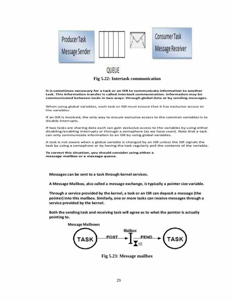
29
Fig 5.22: Intertask communication
Fig 5.23: Message mailbox
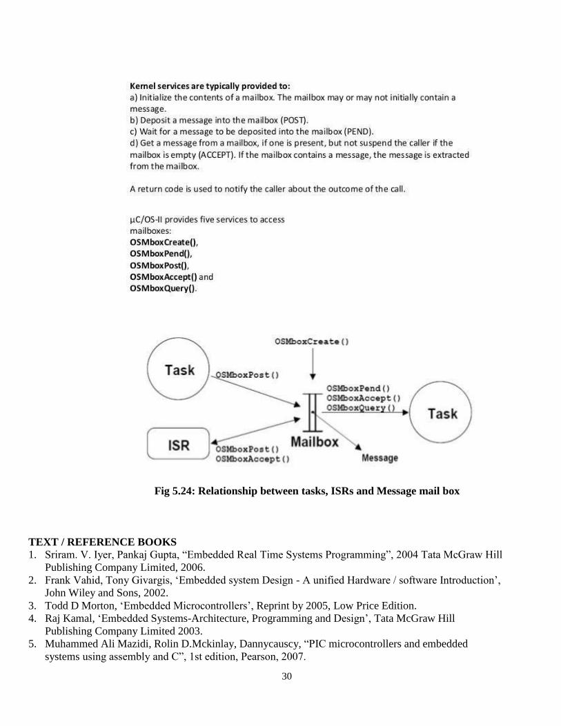
30
Fig 5.24: Relationship between tasks, ISRs and Message mail box
TEXT / REFERENCE BOOKS
1. Sriram. V. Iyer, Pankaj Gupta, ―Embedded Real Time Systems Programming‖, 2004 Tata McGraw Hill
Publishing Company Limited, 2006.
2. Frank Vahid, Tony Givargis, ‗Embedded system Design - A unified Hardware / software Introduction‘,
John Wiley and Sons, 2002.
3. Todd D Morton, ‗Embedded Microcontrollers‘, Reprint by 2005, Low Price Edition.
4. Raj Kamal, ‗Embedded Systems-Architecture, Programming and Design‘, Tata McGraw Hill
Publishing Company Limited 2003.
5. Muhammed Ali Mazidi, Rolin D.Mckinlay, Dannycauscy, ―PIC microcontrollers and embedded
systems using assembly and C‖, 1st edition, Pearson, 2007.