probing interfacial processes on carbon …probing interfacial processes on carbon nanotubes and...
TRANSCRIPT
PROBING INTERFACIAL PROCESSES ON
CARBON NANOTUBES AND GRAPHENE
SURFACES
A THESIS
SUBMITTED TO THE DEPARTMENT OF PHYSICS
AND THE GRADUATE SCHOOL OF ENGINEERING AND SCIENCE
OF BILKENT UNIVERSITY
IN PARTIAL FULFILLMENT OF THE REQUIREMENTS
FOR THE DEGREE OF
MASTER OF SCIENCE
By
Nurbek Kakenov
August, 2012

ii
I certify that I have read this thesis and that in my opinion it is fully adequate, in scope
and in quality, as a thesis for the degree of Master of Science.
.
Asst. Prof. Dr. Coşkun Kocabaş
I certify that I have read this thesis and that in my opinion it is fully adequate, in scope
and in quality, as a thesis for the degree of Master of Science.
.
Prof. Dr. Oğuz Gülseren
I certify that I have read this thesis and that in my opinion it is fully adequate, in scope
and in quality, as a thesis for the degree of Master of Science.
.
Prof. Dr. Raşit Turan
Approved for the Graduate School of Engineering and Science:
.
Prof. Dr. Levent Onural
Director of the Graduate School

iii
ABSTRACT
PROBING INTERFACIAL PROCESSES ON CARBON NANOTUBE
AND GRAPHENE SURFACES
Nurbek Kakenov
M.S. in Physics
Supervisor: Asst. Prof. Dr. Coşkun Kocabaş
August, 2012
The surface of low-dimensional carbon (carbon nanotubes and graphene) has unique
electronic properties due to the delocalized p-orbitals. Very high carrier mobility with
nanoscale dimension make carbon nanotubes and graphene promising candidates for
high performance electronics. Besides electronic properties, the delocalized orbitals
have a strong tendency to adsorb aromatic molecules via p-electronic interactions. The
strong non-covalent interactions between the graphitic surface and organic molecules
provide a unique template for supramolecular chemistry and sensing applications. A
comprehensive understanding of these forces at atomic and molecular level still
remains a challenge. In this thesis, we have used carbon nanotube networks and
graphene as model systems to understand molecular interactions on carbon surface. We
have developed processes to integrate these model materials with sensitive and surface
specific sensors, such as surface plasmon sensor and quartz crystal microbalance. In the
first part of the thesis, we integrated surface plasmon resonance (SPR) sensors with
networks of single-walled carbon nanotubes to study interactions between SWNT and
organic molecules. In the second part, we probe interfacial processes on graphene
surface by mass detection. We anticipate that the developed methods could provide a
sensitive means of detecting fundamental interaction on carbon surfaces.
Keywords: binding parameter, carbon nanotube, chemical adsorption, CVD, graphene,
quartz crystal microbalance, surface plasmon resonance sensor.

iv
ÖZET
KARBON NANOTÜP VE GRAFEN YÜZEYLERİNDEKİ ARA-
YÜZEYSEL ETKİLEŞMELERİN SONDALAMASI
Nurbek Kakenov
Fizik, Yüksek Lisans
Tez Yöneticisi: Asst. Prof. Dr. Coşkun Kocabaş
Ağustos, 2012
Düşük boyutlu karbon (nanotüpler ve grafen) yüzeyi delokalize p-orbital ile sıradışı
elektronik özellikler gostermektedir. Nanometre boyutu ile birlikte çok yüksek elektron
hareketliliğine sahip olan karbon nanotüpler ve grafen yüksek performanslı elektronik
alanında umut verici adaylar olarak belirtiliyolar. Benzersiz elektronik özelliklerinin
yanı sıra, delokalize p-orbital etkileşim yoluyla aromatik moleküllerin güçlü emilme
eğilimi vardır. Grafitik yüzey ve organik molekülleri arasındaki güçlü etkileşimler
supramoleküler kimya ve bioalgılama uygulamaları için yeni bir platform sunmaktadır.
Bu etkileşimlerin mekanizmaları atomik ve moleküler seviyede kapsamlı bir şekilde
anlaşılamamıştır. Bu etkileşmeleri anlamak için yüksek duyarlılıga sahip yeni teknikler
ile düşük boyutlu karbon yüzey üzerindeki organik moleküllerin dinamiğini araştırma
ihtiyacı bulunmaktadır. Bu tezde, karbon yüzey üzerindeki moleküler etkileşimleri
anlamak için model sistemler olarak karbon nanotüp ağları ve grafen kullanmıştır. Biz
yüzey plazmon sensörü ve kuvartz kristal mikroterazi gibi hassas ve yüzeye özel
sensörler ile bu model malzemeleri entegre yollarını geliştirdik. Tezin ilk bölümünde
tek duvarlı karbon nanotüp rin ağlarını yüzey plazmon rezonans sensörlerini kullanarak
karbon nanotüp ve organik moleküllerin arasındaki etkileşimleri inceledik. İkinci
bölümde ise, grafen yüzeyindeki ektileşimleri kütle ölçümü ile araştırdık.
Anahtar sözcükler: bağlanma parametresi, karbon nanotüp, kimyasal adsopsiyon,
CVD, grafen, yüzey plasmon resonans, kuvartz kristal mikroterazi.

v
Acknowledgement
I express my most sincere gratitude and appreciation to Asst. Prof. Dr. Coşkun
Kocabaş. Not only his guidance and support have always leaded me, but also motivated
me during the whole time of my research work. Without his instructions and supportive
attitude, this thesis would not have been possible.
I as well present my gratitude to Prof. Dr. Oğuz Gülseren and Prof. Dr. Raşit Turan for
their judgments and helpful critics as the Master’s Thesis committee.
I also would like to thank all the Kocabaş group and ARL members for providing
wonderful atmosphere during the course of two years.
Above all, I am grateful to Osman Balcı for his support, guidance, and mentorship
throughout the years I have spent in Bilkent.
I am indebted to Şerafettin Küçükoğlu my chemistry teacher, for helping me build the
very first steps of my scientific endeavor.
Most of all I am thankful to Özlem Yavaş for always being supportive, caring, and
joyful. Her cheerful attitude and her being always by my side could not have made the
days of studying much easier, enjoying, and entertaining.
I owe my profound gratitude to my family. Without their love and care it would not
have been possible to do any of this, and without them nothing I do would matter. And
I dedicate this thesis work to my beloved grandmother Shaken Seylakunova with
whom I associate all the good things that our family has.

vi
Contents
1. Introduction ................................................................................................................. 1
1.1 Carbon Based Nanomaterials ................................................................................ 1
1.2 Organization of the thesis ...................................................................................... 2
2. Molecular interactions on carbon surfaces .................................................................. 4
3. Properties and Synthesis of SWNT and Graphene ...................................................... 8
3.1 Single Wall Carbon Nanotubes ............................................................................. 8
3.2 Graphene ............................................................................................................. 13
3.3 Synthesis of Single Wall Carbon Nanotubes ...................................................... 17
3.3.1 Arc discharge evaporation method ........................................................ 17
3.3.2 Laser ablation method ............................................................................ 18
3.3.3 High-pressure carbon monoxide method ............................................... 19
3.3.4 Chemical vapor deposition method ....................................................... 20
3.4 Synthesis of graphene .......................................................................................... 25
3.4.1 Mechanical exfoliation .......................................................................... 25
3.4.2 Thermal decomposition of SiC .............................................................. 26
3.4.3 Chemical vapor deposition synthesis of graphene ................................. 26
4. Probing Molecular Interactions on Carbon Nanotube Surfaces ................................ 32
4.1 Surface plasmon polariton ................................................................................... 32
5. Probing Interfacial Processes on Graphene ............................................................... 47
5.1 Interfacial mass detection with piezoelectric transducers ................................... 47
5.2 Integration of graphene with QCM ..................................................................... 49
6. Summary and future work ......................................................................................... 60

vii
7. Bibliography: ............................................................................................................. 62
viii
List of Figures
Figure 3-1 Schematic representation of the honeycomb lattice. The chiral vector
is a combination of unit vectors, and specified
by the chiral angle . At zigzag line chiral angle is defined to be zero.
defines typical 1D unit cell for SWNTs, lattice vector. ................................. 10
Figure 3-2 (a) Tight-binding band diagram of single sheet graphite plane. (b) Allowed
k-vectors of the (4, 4) and (5, 0) indexed tubes (brown lines). Note that the (4,
4) is metallic the line cross Dirac points, whereas the (5, 0) is semiconducting
tube the lines do not cross Dirac points. Figures were adapted from
mathematica simulations developed by Jessica Alfonsi (University of Pandova,
Italy)................................................................................................................... 11
Figure 3-3 Diagram for possible combinations of indices (n, m) including armchair,
zigzag and chiral types of carbon nanotubes. All armchair SWNTs are defined
to be metallic whereas, only some combinations of zigzag behave like metals. 12
Figure 3-4 (a) Honeycomb lattice structure and (b) Brillouin zone. and are the
primitive unit vectors. The corner points are called as Dirac points K and K'. . 14
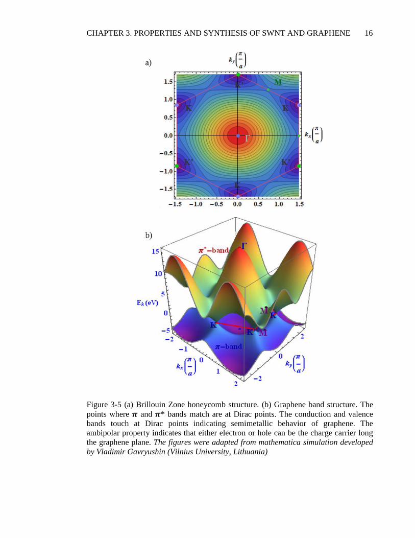
Figure 3-5 (a) Brillouin Zone honeycomb structure. (b) Graphene band structure. The
points where and * bands match are at Dirac points. The conduction and
valence bands touch at Dirac points indicating semimetallic behavior of
graphene. The ambipolar property indicates that either electron or hole can be
the charge carrier long the graphene plane. The figures were adapted from
mathematica simulation developed by Vladimir Gavryushin (Vilnius University,
Lithuania) .......................................................................................................... 16
Figure 3-6 Schematic of arc-discharge evaporation method. High current is applied to
graphite electrodes in ambient He gas. .............................................................. 18

ix
Figure 3-7 Schematics for laser ablation method. High power pulses are incident on
graphite source while maintaining ambient temperature at 1200 . ................. 19
Figure 3-8 Schematics for CVD technique. Hydrocarbons, feedstock of carbon atoms,
decompose by catalyst particles at elevated temperatures. ................................ 20
Figure 3-9 CVD system equipment for SWNT growth. CVD system contains (a)
furnace with inside quartz silica tube vacuum chamber system, (b) gas flow
control units and (c) the sample close-up inside furnace. (d) SEM image of
SWNT network. ................................................................................................. 23
Figure 3-10 Raman spectrum of single wall carbon nanotube. D- and G’ bands indicate
disorders whiles G-band carries graphitic nature. ............................................. 24
Figure 3-11 SWNT transfer-print process on gold metal surface step diagram. ........... 25
Figure 3-12 CVD system equipment for graphene growth. CVD equipment includes (a)
gas flow control units, (b) sample close-up inside furnace, (c) furnace and inside
quartz silica tube integrated with vacuum chamber system. ............................. 29
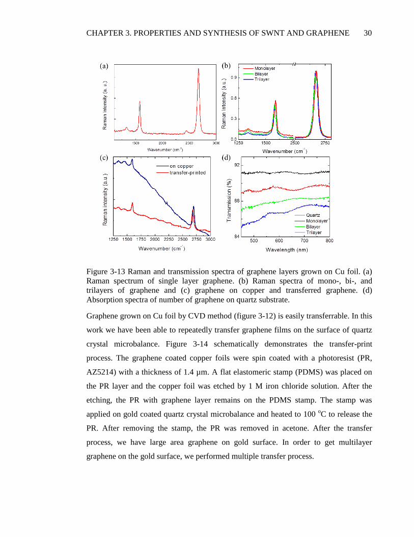
Figure 3-13 Raman and transmission spectra of graphene layers grown on Cu foil. (a)
Raman spectrum of single layer graphene. (b) Raman spectra of mono-, bi-, and
trilayers of graphene and (c) graphene on copper and transferred graphene. (d)
Absorption spectra of number of graphene on quartz substrate. ....................... 30
Figure 3-14 Schematics for transfer-print procedure of graphene sheet on quartz crystal
surface. ............................................................................................................... 31
Figure 4-1 Dispersion curve of surface plasmon polaritons at at metal/air and
metal/glass interfaces. Light line in prism is tilted enabling momentum energy
match for SPP excitations. The plasmons at the metal/glass interface cannot be
excited since the dispersion curve is out of light cone. ..................................... 33
Figure 4-2 Surface plasmon polariton excitation geometries. a) Kretschmann
configuration b) Otto configuration. .................................................................. 35
Figure 4-3 Transfer printing process of SWNT network grown on SiO2 coated Si
substrates. .......................................................................................................... 36
Figure 4-4 Electron micrographs of SWNT networks with various tube densities grown
by chemical vapor deposition on SiO2 substrates. Tube density was controlled
by changing the concentration of the catalyst. These networks are named as sub-

x
monolayer (D1=1 SWNT/µm2), monolayer (D2=10 SWNT/µm
2) and multilayer
(D3=50 SWNT/µm2), respectively. The tube diameter ranges between 0.7 nm to
4 nm. .................................................................................................................. 38
Figure 4-5 Experimental setup (Kretschmann configuration) used to excite SPP on
metal surface coated with SWNT network. The thickness of the gold layer is 50
nm. The prism is mounted on a double rotary state. The reflected beam is
detected by a photodiode. The incidence angle and the wavelength of the laser
are controlled with a precision of less than 0.01 deg. and 1 nm, respectively. . 40
Figure 4-6 The reflectivity maps (angular dispersion curves) from the SWNT coated
gold surface as a function of incidence angle and the excitation wavelength. The
light source is TM polarized. As the density of SWNTs network increases, the
effective index of the surface plasmon-polaritons increases resulting in a red
shift in the plasmon resonance wavelength. The color map shows the scale for
the reflectivity. ................................................................................................... 41
Figure 4-7 (a) Reflection spectra from the gold surface for various tube densities. The
incidence angle is 44 deg. There are two resonances in the reflectivity spectra;
bulk plasmon resonance of around 450 nm and surface plasmon resonance of
around 600 nm. (b) Reflectivity of the surface as a function of incidence angle
for various surface coverage. (c,d) Dependence of surface plasmon resonance
wavelength and angle on the surface coverage of SWNT networks, respectively.
........................................................................................................................... 43
Figure 4-8 (a) Schematic representation of the microfluidic device integrated with SPR
sensor functionalized with SWNT network. The flow chamber is sealed on
SWNT coated gold surface. The glass slide is attached on the prism using an
index matching fluid. (b) Reflectivity of the gold surface as a function of
incidence angle at 635 nm. The resonance angle is 57 deg. (c) Time trace of
SPR signal for binding interaction of BSA on gold surface coated with various
SWNT network. The concentration of BSA is 100 nm. (d) The extracted
parameter (β) quantifies the available binding sites on the surface of SPR
sensor. The β-parameter for gold and submonolayer SWNT networks is around
0.35. As the density of SWNT increases the β-parameter changes from 0.35 to

xi
0.8 while the association constant stays constant with a value of 0.56x10⁵ M
-1
sec-1
. ................................................................................................................... 45
Figure 5-1 Transfer-printing process of graphene on the front electrode of a quartz
crystal microbalance. ......................................................................................... 50
Figure 5-2 (a) Experimental set-up used for probing resonance characteristic of the
QCM. A two-port network analyzer is used to measure scattering parameters.
(b) Magnitude (blue lines) and phase (red lines) of the measured scattering
parameter S11 of the port-1, as a function of frequency for blank (solid line) and
graphene coated QCM (dot line). The resonance frequency is 5,007,323.4 Hz.
The Q-factor of the resonator is around 22600. After coating the surface of
QCM with 0.64 cm2
graphene, we observed around 20 Hz shift in the resonance
frequency. .......................................................................................................... 52
Figure 5-3 Magnitude (a) and phase (b) of scattering parameters measured for QCM
coated with multilayer graphene. (c) Measured frequency shift as a function of
number of graphene layers. The frequency shift shows a linear dependence on
the graphene layers. (d) The bandwidth of the QCM vs. number of graphene
layers. ................................................................................................................. 55
Figure 5-4(a) Schematics of the experimental setup used to probe the time trace of the
resonance frequency of the QCM. (b) Overlaid time trace of resonance
frequency indicating the binding kinetics of Bovine serum albumin (BSA)
proteins on the bare QCM surface and graphene coated QCM surface. The
concentration of BSA is 100nM. ....................................................................... 57
Figure 5-5 Probing oxidation of graphene by mass detection. (a) Change of the
resonant frequency and associated mass uptake of graphene exposed to mild
oxygen plasma. (b) Raman spectra of graphene with various exposure times.
(c-f) Mass uptake of graphene and correlated with Raman intensity for D, G and
2D bands. ........................................................................................................... 59

xii
To my grandmother

1
Chapter 1
1. Introduction
1.1 Carbon Based Nanomaterials
Carbon atoms play an essential role both in our-life-cycle and technology. Their use
has been of great importance in many applications. With the discovery of new carbon
materials like carbon nanotubes [1] and graphene [2], there has been great efforts [1, 3,
4] to implement their extraordinary properties in various devices. Such nanomaterials
possess unique electronic conductance, mechanical strength, optical response, and
thermal transport [1, 2] which make them very attractive in biosensing [5] and in many
other applications.
The surface of low-dimensional carbon (carbon nanotubes and graphene) has unique
electronic properties due to the delocalized p-orbitals. Very high carrier mobility
together with nanoscale dimension makes carbon nanotubes and graphene promising
candidates for high performance electronics [6-11]. Besides unique electronic
properties, the delocalized orbital has a strong tendency to adsorb aromatic molecules
via p-electronic interactions. The strong non-covalent interactions between the
graphitic surface and organic molecules provide a unique template for supramolecular
chemistry [12-14] and sensing applications [15-17]. A comprehensive understanding of
these forces at atomic and molecular level still remains a challenge. A great deal of
computational [18-21] and experimental effort [14, 17, 20, 22-26] has been done to
elucidate these interactions. New techniques with improved sensitivities are needed to
probe the dynamics of organic molecules on the surface of low-dimensional carbon.

CHAPTER 1. INTRODUCTION 2
In the literature, adsorption of molecules on carbon surfaces has been studied
extensively. The earlier works are based on bulk measurements using sorption
isotherms[27-29] and calorimetric studies[30]. Recently, sensitive techniques have
been demonstrated. Schedin et. al.[31] have demonstrated detection of a single
molecule adsorbed on graphene surface by tracing changes in the Hall resistivity of
graphene. Barone et. al.[32] have demonstrated near-infrared optical sensors based on
modulation of emission of SWNT in response to adsorbed biomolecules. Electrical
response of SWNTs in transistor geometry was also used for detecting adsorbed
molecules [15, 16, 33]. Carbon nanotube based capacitive sensors [34], electrochemical
sensors [35], and flow sensors [36] are good examples for methods to detect adsorbed
molecules on nanotube surface.
In this thesis we studied interfacial processes on carbon surfaces using two model
materials; carbon nanotubes and graphene. We have used surface plasmon sensors
(SPR) and quartz crystal microbalance (QCM) to probe interfacial processes on carbon
nanotube and graphene surfaces. Both methods are surface-specific and widely used
especially in biosensing as well as in chemical and surface studies. Any change in the
active medium specifically foreign mass depositions can sensitively be detected by
SPR and QCM approaches. Although, two methods employ different basis for
detections both are capable of sensing similar quantities of measurand with comparable
sensitivities, SPR being more sensitive. The working principle of such techniques
surface plasmon resonance (SPR) and quartz crystal microbalance (QCM) are
described in the following chapters.
1.2 Organization of the thesis
The primary aim of the thesis is to elucidate interfacial processes on carbon surfaces.
We have used carbon nanotube and graphene as model systems to understand
molecular interactions on carbon surface. We have developed processes to integrate
these model materials with sensitive surface specific sensors, such as surface plasmon
sensor and quartz crystal microbalance.

CHAPTER 1. INTRODUCTION 3
Chapter 1 introduces low-dimensional carbon materials as well as their perspectives on
chemical adsorption processes, and viable probing methods.
Chapter 2 reviews the literature on the adsorptions mechanisms of the organic
chemicals on surface graphitic carbon.
Chapter 3 presents fundamental properties of carbon nanotubes and graphene. The
crystal structure and electronic properties will be discussed. Furthermore, their
synthesis methods are described.
Chapter 4 presents a method for probing molecular interaction on single-walled
nanotube surfaces using surface plasmon sensor. SWNT networks were synthesized by
chemical vapor deposition and transfer-printed on gold surfaces. We studied the
excitation of surface plasmon-polaritons on nanotube coated gold surfaces with sub-
monolayer, monolayer, and multilayer surface coverage. Integrating the fabricated
sensor with a microfluidic device, we were able to obtain binding dynamics of a bovine
serum albumin (BSA) protein on SWNT networks with various tube densities. The
results reveal the kinetic parameters for nonspecific binding of BSA on SWNT surface
for various tube densities.
Chapter 5 presents a method for probing interfacial processes on graphene surface
using mass detection. Graphene layers were synthesized by chemical vapor deposition
on copper foils and transfer-printed on a quartz crystal microbalance (QCM). Probing
the mechanical resonance of the QCM, we were able to measure mass density of single
layer graphene. We extended the developed technique to probe binding dynamics of
proteins on graphene surface. Furthermore, we monitored oxidation of graphene
surface under oxygen plasma by tracing the changes of interfacial mass of the graphene
layer.
Chapter 6 provides a summary of the study. Future prospects of this research are also
discussed.

4
Chapter 2
2. Molecular interactions on carbon
surfaces
The mechanism behind the interactions between carbon based nanomaterials and
organic chemical are not fully understood. Still there remain issues such as quantitative
determination of sorption sites, parameters etc. But extensive work has been conducted
to analyze such adsorptions on the surface of carbon nanomaterials. In this chapter we
would like to review the literature in this field.
B. Pan and B. Xing have presented a review on the adsorption properties of carbon
nanotubes and the parameters which have direct impacts on the binding of organic
chemicals to carbon surfaces [24]. In particular, they have claimed that the adsorption
mechanisms are highly dependent on heterogeneity and hysteresis of carbon nanotube
(CNT) and organic molecules interactions, along with hydrophobic interactions,
bonds, electrostatic interactions, and hydrogen bonds.
According to B. Pan et al. organic molecule adsorption on carbon nanotubes cannot be
explained by only one adsorption coefficient due to subsequent errors when forecasting
the interaction of CNTs and chemicals. Various models [37-46] have been proposed to
specify the adsorption of chemicals on CNT. Authors came up with the two
explanations concerning heterogeneous adsorption. That’s, high energy adsorption state
such as carbon nanotube defects [47], functional groups [22] and regions between CNT
bundles [48] are presented as first reason while second one is related to condensation of

CHAPTER 2. MOLECULAR INTERACTIONS ON CARBON SURFACES 5
absorbates. For instance, surface condensation is a process when first two coverings
engage with CNT surface while subsequent ones interact with each other. Similarly,
hysteresis, defined as the discrepancy between adsorption and desorption, for
adsorption of tiny molecules like methane, ethylene, benzene, butane, PAHs, and
atrazine on tubes has been observed. As a result, miscellaneous hysteresis was revealed
suggesting different outcomes for certain circumstances. These outcomes directly
affect future treatments, for instance, depending on hysteresis CNTs can act both as
toxics pollutant collector [49] and like reducer pollutant sinks [50]. Thus, properly
perceiving hysteresis structure is crucial in determining CNT applications and risks.
Various processes like stacking of benzene-ring solutions with nanotube surfaces
[51, 52] and capillary condensations [53] have been accounted for hysteresis.
Moreover, the rearrangement of the adsorbent structures [54], applicable to CNT and
organic chemicals adsorption, is another explanation for hysteresis. In fact,
bonding of organic molecules prevented CNT bundle formation, and by so doing
caused variations in adsorption and desorption processes. As for the shortage of
hysteresis, the lack of CNT bundling is accounted causing no available interstitial
places for molecule adsorptions. Based on the study, there occur another multiple
mechanisms which act simultaneously. That’s, hydrophobic interactions, provided by
individual tubes external surface, can cause molecules of protein, naphthalene, acidic
herbicides, and streptavidin to be adsorbed on CNT. In case the hydrophobicity is sole
effect responsible for the adsorptions then it would be easy to predict the interactions of
chemicals with CNTs by considering parameters like (octane water distribution
coefficient) or (hexadecane water distribution coefficient). However, this is not
completely true. Hydrophobic interaction cannot fully explain the behavior of organic
chemical and CNTs. Mainly due to the lack of strong correlation between the
hydrophobicity for aromatics and affinity of adsorbents [55], high variation in
parameter for organics on CNT and so forth. Other aspects like
interactions, hydrogen bonds, and electrostatic behavior are among simultaneously
acting mechanisms. To predict the organic molecule’s adsorption on CNTs
contributions of individual mechanisms to overall system (adsorption) must be
considered since various mechanisms respond differently to ambient conditions. Hence

CHAPTER 2. MOLECULAR INTERACTIONS ON CARBON SURFACES 6
authors proposed three approaches to disclose the relative contributions of a specific
mechanism. Firstly, the hydrophobic effect can be excluded by normalizing the
sorption coefficients by thus enabling attention to other mechanism [55]. Next,
the adsorption of diverse organic chemicals on a certain type of tubes can be compared
which can reveal useful information. Lastly, direct sorption experiments can be run in
an environment of organic solvents.
Another essential effect on adsorption process can be accounted for the properties of
CNTs. As compared to activated carbon (AC) carbon nanotube has lower surface area
( ) [56]. Nevertheless, the adsorption of organic molecules on SWNT
is higher than that of ACs [57]. This suggests that surface area might not be sole
attribute when considering chemicals and CNT interactions. While higher surface areas
can have strong adsorption strength [46, 58, 59], it is not the case for molecules with
planar structure. Since flat surfaces enable better contact to such molecules [60, 61].
Thus, none of the parameters like diameter, porosity, and surface area could
individually explain fully the adsorption characteristics of CNT. Furthermore,
morphology of carbon nanotubes suggests that the surface area, interstitial and groove
regions within CNT-bundles and inside regions of the tubes are accessible sites for
sorption. Outer surface and trench regions are mainly open for adsorptions; however,
inner sides are closed due to dimensional restrictions. Nonetheless, some molecules
like enzymes with the size 3-5 nm are reported to be adsorbed in the inner pores of
tubes [62]. Moreover, these inner pores can be blocked by molecules such as
amorphous carbon, functional groups, and catalyst nanoparticles. Lack of bundling of
CNTs could be another reason for inaccessible interstitial sites [44] or it might be huge
molecules which fail to fit in the sites [63]. Hence the readiness of the site for organic
chemical adsorptions on CNTs are greatly relies on the properties of the carbon
nanotubes and their accumulations. Another nature, which affects the adsorptions, is
the chirality of the tubes. Although, bonds are the same kind in the plane of
graphite, it is not the case for zigzag, armchair and chiral types of CNTs varying by
length and positions to the axis of tubes [60].
CHAPTER 2. MOLECULAR INTERACTIONS ON CARBON SURFACES 7
The functional groups like can be included in CNTs. These
groups can alter the surface of carbon nanotubes to be more hydrophilic and fitted for
the polar molecule adsorptions [43, 64, 65]. However functional groups may also cause
the higher diffusional resistance [66] and reduction of availability and attraction of
tubes surfaces [56, 67]. Besides, since there is delocalized orbit in every atom in
CNT this can result in the formation of bonds [68] between organic molecules,
assuming latter contain such orbit as well. In addition, the polarity and non-polarity
of molecules being adsorbed on CNT highly needs different approaches. For instance,
polar organic molecules are adsorbed greatly due to high CNT oxygen content. On the
other hand, hydrophobic effect the adsorption is low for nonpolar organics within the
environment of intensified CNT oxygen content.
As authors report, the SWNTs have shown to be superior to ACs and other adsorbents
not only with higher adsorption capacity [41, 43, 69] but with also higher adsorption
energy [70], along with the faster equilibrium time [43, 64, 69], and with more efficient
regeneration [39, 41]. Similarly SWNTs possess higher adsorption coefficients as
compared to ACs. Consequently, SWNT is viable material candidate to be used in air
purification and water clearance.
As discussed, many diverse factors determine the interactions between organic
chemicals and carbon nanotube affected differently by the ambient conditions. Each
mechanism may have different consequences on adsorption process. When H-bond
mechanism is superior, for example, the functional groups with higher oxygen content
would undergo greater sorption on CNTs, whereas, when hydrophobic behavior is
predominant, the affinity and availability of CNT is low for organic chemicals. Thus, it
is essential to have greater understanding about the relative contributions of adsorption
mechanisms to the entire sorption process.

8
Chapter 3
3. Properties and Synthesis of SWNT and
Graphene
This chapter presents fundamental properties of carbon nanotubes and graphene. The
crystal structure and electronic properties will be discussed. Furthermore, their
synthesis methods are described.
3.1 Single Wall Carbon Nanotubes
Carbon nanotubes were discovered by Iijima in 1991 at NEC Laboratory [1]. Following
years single-wall carbon nanotubes (SWNTs) were synthesized using the same
technique. The structure and properties of SWNT were substantially studied by many
scientists stimulated by 1D quantum effects.
SWNT is a cylinder formed from honeycomb crystalline of graphene sheet. The
structure of single-wall carbon nanotube is a collection of 1D unit cell defined by the
vectors and T in figure 3-1. The circumference of any carbon nanotube is expressed
in terms of the chiral vector two sides of graphene layer. The
formation wholly depends on the pair of integers (n, m), which specify chiral vector,
and chiral angle. In fact, chiral angle is defined as the angle between chiral vector and
“zigzag” orientation ( as depicted in figure 3-1. Theoretically three distinct types
of carbon nanotubes can be constructed by rolling up the graphene sheet. If the chiral
angles are 0 and 30 degrees it corresponds to zigzag and armchair types respectively,
and if the chiral is between to extremes ( then it becomes chiral type of the

CHAPTER 3. PROPERTIES AND SYNTHESIS OF SWNT AND GRAPHENE 9
carbon nanotube. The translational vector, T, is the vector perpendicular to chiral
vector, and these vectors define the unit cell of 1D lattice (see figure 3-1). For the chiral
vector with (n, m) indices zigzag and armchair can be obtained for (n, 0) and (n, n) in
(n, m) notation. All other combinations represent chiral geometry. Furthermore, the
nanotube diameter, , is represented by
√ (
(3.1)
where , is the bond length (1.42 ), and the chiral angle is given by
[√
] (3.2)
The angle of zigzag nanotube (n, 0) would be and armchair nanotube (n, n)
would have value, and hence by symmetry the chiral angle can be assigned to
boundary. Both zigzag and armchair are considered as achiral type while
chiral type carbon nanotubes have any angle values within boundary except extreme
angles 0 and 30. Another significant parameter describing SWNT structure is number
of hexagons, N, per unit cell of a chiral nanotube, defined by indices (n, m) is
represented in the equation
( (3.3)
where if is a multiple of , if is not a multiple of ,
and is the largest common divisor of (n, m).

CHAPTER 3. PROPERTIES AND SYNTHESIS OF SWNT AND GRAPHENE 10
Figure 3-1 Schematic representation of the honeycomb lattice. The chiral vector
is a combination of unit vectors, and specified by the
chiral angle . At zigzag line chiral angle is defined to be zero. defines typical
1D unit cell for SWNTs, lattice vector.
Studies [71, 72] have shown that geometric structure of carbon nanotubes affects their
electronic properties. Despite graphene has zero band gap and considered as semimetal,
carbon nanotubes can be classified into metals and semiconductors which highly relies
on diameter and helicity of the tubes [73]. Dresselhauss et al. in their study have
summarized the band-folding picture by the unique band structure of mono-layer
graphite plane, which has only six crossings of Fermi level in k-space, and by the
quantization k-momentum of electron along circumferential line [72]. Accordingly,
graphene sheet is a zero-band-gap semiconductor, and its electronic structure is given
by the occupied and unoccupied * bands. Figure 3-2, depicts point in the
Brillouin zone where linearly dispersed two bands coincide at the Fermi level. There
are six such K points at each corner of the honeycomb structure. Periodical boundary

CHAPTER 3. PROPERTIES AND SYNTHESIS OF SWNT AND GRAPHENE 11
conditions established in circumferential direction, dictate that the allowed k states,
highly dependent on radius and helicity of carbon nanotubes, in the graphitic plane. If
allowed k states involve the point, then the structure is metallic two bands possessing
linear dispersion at the Fermi level. Also if, the K point is not contained the structure
exhibits semiconducting property with various band gaps.
Figure 3-2 (a) Tight-binding band diagram of single sheet graphite plane. (b) Allowed
k-vectors of the (4, 4) and (5, 0) indexed tubes (brown lines). Note that the (4, 4) is
metallic the line cross Dirac points, whereas the (5, 0) is semiconducting tube the lines
do not cross Dirac points. Figures were adapted from mathematica simulations
developed by Jessica Alfonsi (University of Pandova, Italy)

CHAPTER 3. PROPERTIES AND SYNTHESIS OF SWNT AND GRAPHENE 12
In fact, chiral indices (n, m) determine the metallic and semiconducting properties of
carbon nanotubes. For instance, (n, n) indexed SWNTs are known to be metals; tubes
(n, m) are metals if where is a nonzero integer at room temperature, and
all others ones are semiconductors. The figure 3-3 classifies some combinations of
metallic and semiconducting single wall carbon nanotubes.
Figure 3-3 Diagram for possible combinations of indices (n, m) including armchair,
zigzag and chiral types of carbon nanotubes. All armchair SWNTs are defined to be
metallic whereas, only some combinations of zigzag behave like metals.
CHAPTER 3. PROPERTIES AND SYNTHESIS OF SWNT AND GRAPHENE 13
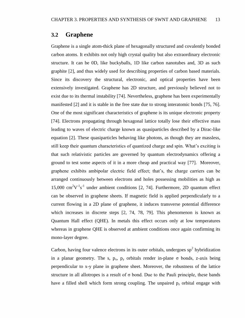
3.2 Graphene
Graphene is a single atom-thick plane of hexagonally structured and covalently bonded
carbon atoms. It exhibits not only high crystal quality but also extraordinary electronic
structure. It can be 0D, like buckyballs, 1D like carbon nanotubes and, 3D as such
graphite [2], and thus widely used for describing properties of carbon based materials.
Since its discovery the structural, electronic, and optical properties have been
extensively investigated. Graphene has 2D structure, and previously believed not to
exist due to its thermal instability [74]. Nevertheless, graphene has been experimentally
manifested [2] and it is stable in the free state due to strong interatomic bonds [75, 76].
One of the most significant characteristics of graphene is its unique electronic property
[74]. Electrons propagating through hexagonal lattice totally lose their effective mass
leading to waves of electric charge known as quasiparticles described by a Dirac-like
equation [2]. These quasiparticles behaving like photons, as though they are massless,
still keep their quantum characteristics of quantized charge and spin. What’s exciting is
that such relativistic particles are governed by quantum electrodynamics offering a
ground to test some aspects of it in a more cheap and practical way [77]. Moreover,
graphene exhibits ambipolar electric field effect; that’s, the charge carriers can be
arranged continuously between electrons and holes possessing mobilities as high as
15,000 cm2V
-1s
-1 under ambient conditions [2, 74]. Furthermore, 2D quantum effect
can be observed in graphene sheets. If magnetic field is applied perpendicularly to a
current flowing in a 2D plane of graphene, it induces transverse potential difference
which increases in discrete steps [2, 74, 78, 79]. This phenomenon is known as
Quantum Hall effect (QHE). In metals this effect occurs only at low temperatures
whereas in graphene QHE is observed at ambient conditions once again confirming its
mono-layer degree.
Carbon, having four valence electrons in its outer orbitals, undergoes sp2 hybridization
in a planar geometry. The s, px, py orbitals render in-plane σ bonds, z-axis being
perpendicular to x-y plane in graphene sheet. Moreover, the robustness of the lattice
structure in all allotropes is a result of σ bond. Due to the Pauli principle, these bands
have a filled shell which form strong coupling. The unpaired pz orbital engage with

CHAPTER 3. PROPERTIES AND SYNTHESIS OF SWNT AND GRAPHENE 14
other neighboring pz orbitals to create π and π* bonds in z-axis direction. As the pz
orbital has one electron, the π band is half filled. The figure 3-4 illustrates the lattice
structure of graphene. The lattice vectors can be written as
( √ )
( √ ), where is a carbon-carbon bond length, and the reciprocal
lattice vector are given by
( √ )
( √ ).
Figure 3-4 (a) Honeycomb lattice structure and (b) Brillouin zone. and are the
primitive unit vectors. The corner points are called as Dirac points K and K'.
The two points at the corner of graphene Brillouin zone (BZ) (see figure 3-
4b) play significant role in graphene’s physics. In momentum space they can be written
as (
√ ) (
√ . As mentioned [74], the low-excitations in
graphene sheet have been observed to be massless, chiral, and Dirac fermions. The
dispersion, valid only at low energies, resembles to massless fermions in quantum
electrodynamics except for that fermions in graphene move with speed , 300 times
slower than the speed of light [78, 80]. The energy band dispersion for hexagon lattice
(see figure 3-5) is expressed by the equation

CHAPTER 3. PROPERTIES AND SYNTHESIS OF SWNT AND GRAPHENE 15
( ) √
√
(3.4)
where are x and y components of momentum vector of electron and is
the nearest-neighboring hopping energy. In figure 3-5, the energy band of honeycomb
lattice structure of graphene is demonstrated. The conduction band and the valence
band coincide at discrete points, called K points. Graphene’s electronic density of states
linearly vanishes with energy at the Dirac point [80]. Thus, neutral graphene is a
combination of a metal and a semiconductor, or can be defined as semimetal. It is not a
metal since its density of state vanishes and nor semiconductor as there is no band gap
in the spectrum, and hence zero energy needed to excite electrons.
CHAPTER 3. PROPERTIES AND SYNTHESIS OF SWNT AND GRAPHENE 16
Figure 3-5 (a) Brillouin Zone honeycomb structure. (b) Graphene band structure. The
points where and * bands match are at Dirac points. The conduction and valence
bands touch at Dirac points indicating semimetallic behavior of graphene. The
ambipolar property indicates that either electron or hole can be the charge carrier long
the graphene plane. The figures were adapted from mathematica simulation developed
by Vladimir Gavryushin (Vilnius University, Lithuania)

CHAPTER 3. PROPERTIES AND SYNTHESIS OF SWNT AND GRAPHENE 17
3.3 Synthesis of Single Wall Carbon Nanotubes
Since the discovery of carbon nanotubes, many studies have focused on the
improvement of synthesis methods. Of them, laser evaporation [81, 82], arc-discharge
[1, 81, 83, 84], HiPco [85-87], and chemical vapor deposition (CVD) [81, 84, 88-90]
methods have been preferably used to yield high quality carbon nanotube. This section
summarizes briefly some techniques and explains in detail chemical vapor deposition
technique.
3.3.1 Arc discharge evaporation method
Arc discharge evaporation can produce both single-walled and multi-walled carbon
nanotubes amongst other carbon forms. In fact, this is the first method to produce
carbon nanotubes [1]. The arc discharge method employs two very close graphite rods
connected to current. When high current passes through electrodes carbon atoms
are ejected from anode and drift toward cathode [91]. Very high temperature (
) needed to vaporize carbon atoms. These ejected carbon atoms deposit
themselves on the surface of cathode in tubular form. Multi-walled carbon nanotubes
grown by arc discharge method possess lower defects, and have better electrical,
thermal, and mechanical properties. In case when metallic nanoparticles are used as
catalysts SWNT can be grown in arc discharge method [1, 81, 83, 84]. The
disadvantage of the arc evaporation is that carbon nanotubes must be purified since
process contains other graphite crystalline. The basic scheme for arc-discharge system
is shown in figure 3-6.

CHAPTER 3. PROPERTIES AND SYNTHESIS OF SWNT AND GRAPHENE 18
Figure 3-6 Schematic of arc-discharge evaporation method. High current is applied to
graphite electrodes in ambient He gas.
3.3.2 Laser ablation method
Laser ablation method is based on vaporizing carbon atoms by laser pulses. A powerful
pulsed laser is used to target carbon source in hot gas atmosphere at 1200ºC [81, 82].
To sustain the reliable condition for growth of carbon nanotube double quartz tube is
utilized in an oven, where the target is pure graphite in an ambient gas such as Ar. It is
crucial to maintain reliable temperature conditions since otherwise no carbon nanotube
would grow. The laser targets the graphite causing ejection of carbon atoms, and those
atoms are caught by flow reach the substrate where it starts to form multi-walled
carbon nanotubes (MWNT). As to generate single-walled carbon nanotubes (SWNT)
the metal catalyst are added to graphite target. The catalyst particles functions to keep
open fullerenes as the additional carbon atoms attach forming nanotubes. As compared
to arc discharge method the nanotubes synthesized by laser ablation are more pure up
to %90. There is less by products like amorphous carbon, fullerenes, and graphitic
clusters since the growth process is confined spatially supporting conditions more
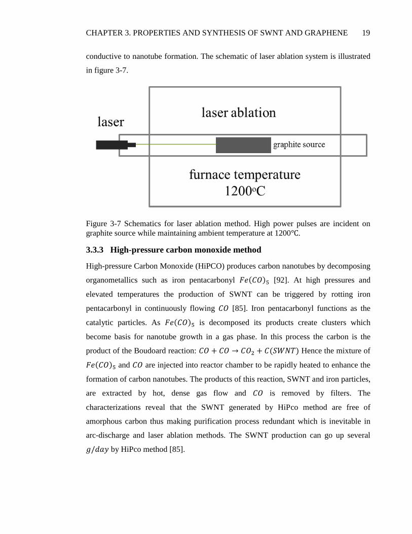
CHAPTER 3. PROPERTIES AND SYNTHESIS OF SWNT AND GRAPHENE 19
conductive to nanotube formation. The schematic of laser ablation system is illustrated
in figure 3-7.
Figure 3-7 Schematics for laser ablation method. High power pulses are incident on
graphite source while maintaining ambient temperature at 1200 .
3.3.3 High-pressure carbon monoxide method
High-pressure Carbon Monoxide (HiPCO) produces carbon nanotubes by decomposing
organometallics such as iron pentacarbonyl ( [92]. At high pressures and
elevated temperatures the production of SWNT can be triggered by rotting iron
pentacarbonyl in continuously flowing [85]. Iron pentacarbonyl functions as the
catalytic particles. As ( is decomposed its products create clusters which
become basis for nanotube growth in a gas phase. In this process the carbon is the
product of the Boudoard reaction: ( Hence the mixture of
( and are injected into reactor chamber to be rapidly heated to enhance the
formation of carbon nanotubes. The products of this reaction, SWNT and iron particles,
are extracted by hot, dense gas flow and is removed by filters. The
characterizations reveal that the SWNT generated by HiPco method are free of
amorphous carbon thus making purification process redundant which is inevitable in
arc-discharge and laser ablation methods. The SWNT production can go up several
by HiPco method [85].

CHAPTER 3. PROPERTIES AND SYNTHESIS OF SWNT AND GRAPHENE 20
3.3.4 Chemical vapor deposition method
Since the discovery, the principal methods for the synthesis of carbon nanotubes were
arc discharge and laser evaporations of carbon feedstock. Both methods have capability
of producing MWNT and SWNT materials. The major issues concerning with these
methods are high temperature ( ) necessity for solid carbon evaporations, and
undesired by-products such as fullerenes, graphitic polyhedrons with enclosed metal
particles, and amorphous carbon which come along with tubular carbon [73]. Hence,
nanotube materials need to go through additional procedures to yield pure carbon
nanotubes. Since many applications require high quality carbon nanotubes, the growth
processes have to be perfected [93]. Significant work has been done to develop defect-
free carbon nanotubes growth and chemical vapor deposition (CVD) method is a
promising candidate. In this section the SWNT growth is discussed.
The CVD process involves the decomposition of hydrocarbons triggered by catalyst
particles at an elevated temperatures and the precipitation of carbon atoms in a tubular
form on the surface, dispersed by transition-metals. The figure 3-8 depicts schematic
representation of CVD system.
Figure 3-8 Schematics for CVD technique. Hydrocarbons, feedstock of carbon atoms,
decompose by catalyst particles at elevated temperatures.
The CVD consists of quartz tube heated in an oven and gas flow system. The gas is
flown through the quartz tube including catalyst particles spread over silicon substrate

CHAPTER 3. PROPERTIES AND SYNTHESIS OF SWNT AND GRAPHENE 21
heated to predetermined temperature. The essential factors of CVD process involve
precursors, catalyst particles, and growth temperature. Carbon precursors utilized in
CVD are mainly hydrocarbons like methane, ethylene, ethanol, carbon monoxide,
acetylene, methanol, benzene, and toluene each possessing particular decomposition
temperature for nanotube formations [90, 94]. In the synthesis of SWNT, the rate of
carbon precursors is of great importance. The increased temperature can result in high
rate of decomposition of hydrocarbon; nonetheless, it can also cause self-pyrolysis of
hydrocarbons [90]. Thus, increased concentrations of amorphous carbon lead to
deactivation of catalyst process [95]. The favored temperatures for carbon nanotube
growth range from [90]. Ideal temperature for growth relies on
primarily preferred carbon feedstock and catalyst. The dynamics of the growth is
highly dependent on the ambient temperature. Other crucial effect of the temperature is
the treatment of readily oxidized catalyst nanoparticles, by bringing back to activated
mode [96]. The catalyst nanoparticles used in CVD process mostly are Fe, Co Mo, Ni,
Cu, Au, etc. knows as transitional-metal nanoparticles [90]. High carbon solubility and
diffusion rates as well as high melting temperatures are essential characteristics to be
exploited in the nanotube formations [94]. One the other crucial function of metals is
the capability to decompose carbonic molecules during the formation of carbon
nanotubes. The catalyst particles can be produced by different fabrication
methodologies [90]. For instance, as Moisala et al noted the precipitation of metal salts
(nitrates, sulfates and chlorides) and organometallic precursor support are widely used
methods[90]. The size distribution of manufactured particle can vary and can be
significantly effective in the time of formation. In fact, it has been proposed that the
size of catalyst particles may directly be related to the diameter of formed carbon
nanotubes [97]. Experimental evidence was conducted by Cheung et al [95], iron
particles with average diameter of 3, 9, and 13 nm yielded carbon nanotubes with 3, 7,
and 12 nm tubule diameters respectively. The typical range for the diameter size of
SWNT is between 0.7 and 4 nm. The smallest size for SWNT is believed to be
confined to that of fullerene size (C60) [73].

CHAPTER 3. PROPERTIES AND SYNTHESIS OF SWNT AND GRAPHENE 22
The exact mechanism for the synthesis of carbon nanotubes is still unclear,
nevertheless, the consensus is that at high temperature the hydrocarbons decompose
into hydrogen and carbon, carbon atoms dissolve and diffuse into the metal surface and
rearrange themselves into a clusters containing hexagons of carbon atoms and finally
precipitate to form carbon nanotubes [73, 81]. There are two modes of the carbon
nanotube formation. When the catalyst particles are strongly bounded to the support the
carbon atom precipitate and begin to grow on top the metal particles which remain
bound to surface. It is called root-growth [81]. Conversely, if the metal particles are
weakly bounded to the support, the carbon atoms start to precipitate from the bottom of
the metal particles suspending them off the surface, called as the tip-growth [81].
The various parameters such as hydrocarbons, catalyst particles, and the formation
temperature are essential in CVD process. Their manipulations to enhance the synthesis
of particular carbon nanotube is what makes CVD method promising.
In this work, we have used CVD system to growth SWNT. Figure 3-9 depicts growth-
setup. It consists of gas tubes of argon and hydrogen, carbon seed bubbler, control unit,
and the furnace. The first step of the process is to prepare catalyst nanoparticles, in our
case iron chloride. Predetermined amount of iron chloride, concentrations of which
affect the SWNT formation, is mixed with photoresist (Shipley 1805). In fact, different
molarities of catalyst solutions readily determine the densities of SWNT network. Then
the photoresist, doped with , is covered on the surface of wafers with a 500 nm
thickness. Annealing photoresist in air can cause oxidation of catalyst nanoparticles.
This process is necessary to remove organic contaminants from the surface of metal
dispersed wafer, in our case silicon oxide. In order to abate iron oxide nanoparticles the
substrate is annealed in hydrogen (300 sccm) at 700 for 20 min. in the quartz tube.
Subsequent to the reduction of iron oxide molecules the growth is started by flowing
ethanol vapor using carrier flow of Ar (50 sccm) and H2 (50 sccm) at 920 . The flow
rates of the gases are controlled by control units. After 15 min. we terminate the growth
and cool sample to room temperature under Ar (1000 sccm) flow.

CHAPTER 3. PROPERTIES AND SYNTHESIS OF SWNT AND GRAPHENE 23
Figure 3-9 CVD system equipment for SWNT growth. CVD system contains (a)
furnace with inside quartz silica tube vacuum chamber system, (b) gas flow control
units and (c) the sample close-up inside furnace. (d) SEM image of SWNT network.
The characterizations of the samples are done by electron microscope and Raman
spectroscopy. The scanning electron microscope (SEM) images (see figure 3-9d) reveal
density and uniformity of the SWNT samples grown by CVD. In a similar fashion, the
Raman spectra indicate the quality and the number of walls for the carbon nanotubes
[98-100]. The peaks at (D-band), (G-band), and
(G’-band) are clear indicator of single wall carbon nanotubes (see figure 3-10).

CHAPTER 3. PROPERTIES AND SYNTHESIS OF SWNT AND GRAPHENE 24
Figure 3-10 Raman spectrum of single wall carbon nanotube. D- and G’ bands indicate
disorders whiles G-band carries graphitic nature.
The samples grown on substrate can be easily transferred to other surfaces. In
our study, SWNT network was transferred to a 50 nm thick gold surface. The property
that gold and carbon nanotube strongly stick together than carbon nanotube is held on
substrate is base for transferring process. Figure 3-11 depicts the procedure.
The SWNT networks were grown by CVD system as described above. We first
evaporated 50 nm thick gold film on the SWNT network. Not only the gold layer
provides mechanical support for SWNT during the transfer process with low adhesion
on SiO2 surface, but it maintains surface for SPPs. We applied the gold coated surface
on a glass slide coated with UV curable polymer. The polymer layer is cured as it
exposed to UV light and hence sticks the gold-SWNT layer to the cured polymer
surface. The SWNT networks transferred on gold surface after mechanically removing
the substrate.
CHAPTER 3. PROPERTIES AND SYNTHESIS OF SWNT AND GRAPHENE 25
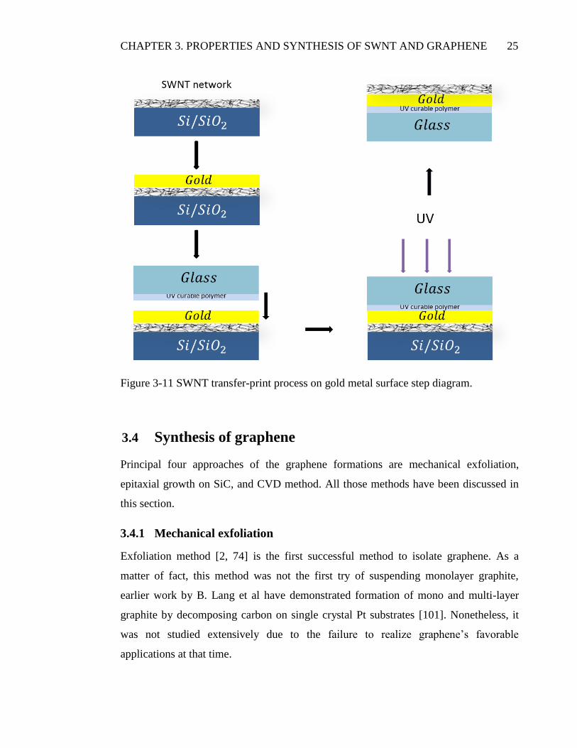
Figure 3-11 SWNT transfer-print process on gold metal surface step diagram.
3.4 Synthesis of graphene
Principal four approaches of the graphene formations are mechanical exfoliation,
epitaxial growth on SiC, and CVD method. All those methods have been discussed in
this section.
3.4.1 Mechanical exfoliation
Exfoliation method [2, 74] is the first successful method to isolate graphene. As a
matter of fact, this method was not the first try of suspending monolayer graphite,
earlier work by B. Lang et al have demonstrated formation of mono and multi-layer
graphite by decomposing carbon on single crystal Pt substrates [101]. Nonetheless, it
was not studied extensively due to the failure to realize graphene’s favorable
applications at that time.

CHAPTER 3. PROPERTIES AND SYNTHESIS OF SWNT AND GRAPHENE 26
Graphite consists of large number of carbon stacks bound by van der Waals force. Van
der Waals force is relatively weak compared to the covalent bonds, enabling possibility
of producing graphene by breaking inter-plane bonds. Exfoliation and cleavage
approaches are based on applying mechanical or chemical energy to crack these bonds
and separating individual graphene sheets [102]. Basically, exfoliation is the process of
peeling. Novoselov et al. [2], have successfully exploited cleavage technique to
produce few layers or even single layer graphene. They have used commercial highly
oriented graphite sheet and dry etched it by exposing to oxygen plasma to make many
deep mesas [2]. The photoresist is used to stick mesas which then removed by scotch
tape to peel off the layers. Resultant thin flakes were found to be single to few layer of
graphene. Exfoliated graphene can be as large as 100µm and are easily transferred to
different substrates.
3.4.2 Thermal decomposition of SiC
One of the first growths of graphitic structures by silicon (Si) sublimation from Silicon
Carbide (SiC) substrates was demonstrated in 1975 [103]. Electronic properties of
those materials were found to be similar to that of isolated graphene [104]. The process
includes thermal decomposition of Si on the surface plane (0001) of 4H- and 6H-SiC
wafer [102]. The formations of graphene sheets caused when SiC wafer is heated to
1500 leading to sublimation of Si atom leaving carbon atoms which then rearrange
themselves into graphene sheets [104]. Such epitaxially grown graphene were found to
have single to few layers [102]. Compatibility of SiC formation of graphene with
standard semiconductor device fabrication technology and capability of large scale
production have attracted attention of semiconductor industries and considered to be
viable technique [104]. A comprehensive review concerning such issue was reported by
J. Hass et al. [105].
3.4.3 Chemical vapor deposition synthesis of graphene
Growing graphene by chemical vapor deposition is considered as the most promising
technique. Its cost, controllability, grain size, etchability and transferability of grown
graphene, and large scale area production are widely accepted in semiconductor
industries [106]. CVD method is capable of producing centimeter sized continuous

CHAPTER 3. PROPERTIES AND SYNTHESIS OF SWNT AND GRAPHENE 27
graphitic sheets. The process involves epitaxial growth of single to few layer graphene
by flowing mixture of methane and hydrogen gases at an elevated temperatures
catalyzed by metals such as Ni, Cu, Co, Pt, and Ir [107]. Methane and Ethanol are
widely used carbon feedstock molecules. Similar to carbon nanotube growth metal
catalysts effectively function the patterned growth of graphene at particular locations
with desired geometries [107]. Catalyst films are responsible for decomposition of
carbon precursor molecules on the surface or within the catalyst itself additionally
providing support graphene during growth process. Copper and nickel are widely used
substrate materials owing to its cost, grain size, and etchability [94]. Carbon
segregation[108] or precipitation[109] is proposed as a process mechanism in CVD
growth of graphene on Ni catalyst substrate Li et al.[94]. Authors note the significance
of the difference in concepts between segregation and precipitation. That’s, according
to them, segregation referred to compositional heterogeneity in thermal equilibrium
under conditions which correspond to a “one phase” field, while precipitation was
caused by inhomogeneities subsequent to equilibrium “phase separation”. Also Li at el.
[94] mentioned spacious variations in thickness from single to multiple layers on metal
surface were discovered on graphene samples grown on Ni foils. The inhomogeneity
was caused by high solubility of carbon atom in nickel. It is claimed that graphene
mono-layer starts to grow by carbon segregation then precipitation induces further top
layer formations [110]. In order to terminate multiple layer growth fast cooling of
samples is necessary. Unlike nickel, copper does not have over saturation due to its low
solubility of carbon atoms in Cu [94]. Additionally, very large grain sizes can be
obtained by annealing copper. This makes copper a viable thin film catalyst candidate
in graphene synthesis. Previous studies showed that graphene films grown on the
surface catalyzed by Cu exhibited predominantly mono-layer with less than %5 two-
and three-layer graphene flakes, and these flakes would not grow larger for with time
[111]. Furthermore, Li at el. have demonstrated that it takes less than 3 min. to grow
single layer graphene, and that the growth is self-limiting due to the lack of catalyst to
promote the growth and thus metals with low carbon solubility provide possibilities for
large-scale growth of graphene.

CHAPTER 3. PROPERTIES AND SYNTHESIS OF SWNT AND GRAPHENE 28
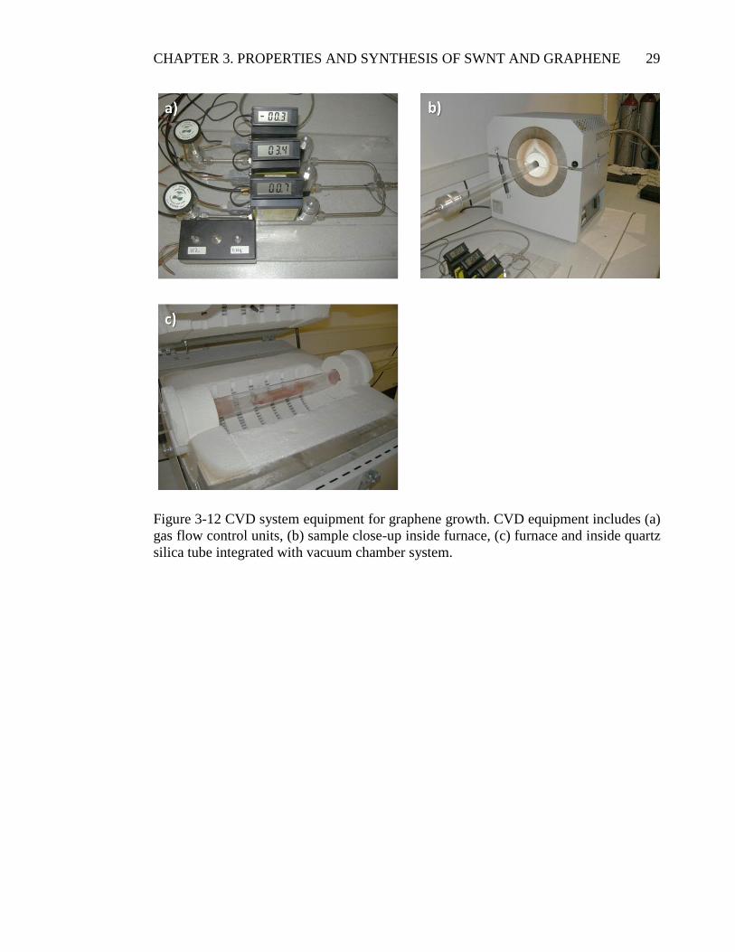
In our experiments, graphene layers were synthesized on copper foils by chemical
vapor deposition (refer to figure 3-12). The copper foils were placed in a quartz
chamber and heated to 1050 oC under flow of hydrogen and argon gases. In order to
reduce the oxide layer, the samples were annealed for 30 min at 1050 oC. After the
annealing process, methane gas with a rate of flow of 7 sccm was sent to the chamber
for 10 min. The chamber pressure was kept at 5 Torr during the growth. The growth
was terminated by stopping the flow of methane gas and the chamber was cooled back
to the room temperature. Figure 3-12 shows chemical vapor deposition set-up for
graphene. The grown graphene can be characterized using Raman spectroscopy.
Typical signal for monolayer graphene is shown in figure 3-13a where the peak at
is G-band and the peak at is 2D band. These bands
demonstrate the distinctions of graphene layer from that of bulk graphite [99]. In
addition, the D-band at represents defect mode. Since, D-band peak is
low the graphene samples indicate high quality. Figure 3-13b shows the Raman spectra
comparison for mono-, bi- and trilayer graphene. As can be seen, there are no
significant distinctions between single and few layers of graphene, and hence behave
alike. Figure 3-13c demonstrates the graphene on copper and transferred graphene. In
figure 3-13d, the transmission spectra of graphene on quartz substrate is depicted. %2
of absorbance is observed for each layer of graphene.
CHAPTER 3. PROPERTIES AND SYNTHESIS OF SWNT AND GRAPHENE 29
Figure 3-12 CVD system equipment for graphene growth. CVD equipment includes (a)
gas flow control units, (b) sample close-up inside furnace, (c) furnace and inside quartz
silica tube integrated with vacuum chamber system.
CHAPTER 3. PROPERTIES AND SYNTHESIS OF SWNT AND GRAPHENE 30
Figure 3-13 Raman and transmission spectra of graphene layers grown on Cu foil. (a)
Raman spectrum of single layer graphene. (b) Raman spectra of mono-, bi-, and
trilayers of graphene and (c) graphene on copper and transferred graphene. (d)
Absorption spectra of number of graphene on quartz substrate.
Graphene grown on Cu foil by CVD method (figure 3-12) is easily transferrable. In this
work we have been able to repeatedly transfer graphene films on the surface of quartz
crystal microbalance. Figure 3-14 schematically demonstrates the transfer-print
process. The graphene coated copper foils were spin coated with a photoresist (PR,
AZ5214) with a thickness of 1.4 µm. A flat elastomeric stamp (PDMS) was placed on
the PR layer and the copper foil was etched by 1 M iron chloride solution. After the
etching, the PR with graphene layer remains on the PDMS stamp. The stamp was
applied on gold coated quartz crystal microbalance and heated to 100 oC to release the
PR. After removing the stamp, the PR was removed in acetone. After the transfer
process, we have large area graphene on gold surface. In order to get multilayer
graphene on the gold surface, we performed multiple transfer process.

CHAPTER 3. PROPERTIES AND SYNTHESIS OF SWNT AND GRAPHENE 31
Figure 3-14 Schematics for transfer-print procedure of graphene sheet on quartz crystal
surface.

32
Chapter 4
4. Probing Molecular Interactions on
Carbon Nanotube Surfaces
This chapter presents a method for probing molecular interaction on single-walled
nanotube surfaces using surface plasmon sensor. SWNT networks were synthesized by
chemical vapor deposition and transfer-printed on gold surfaces. We studied the
excitation of surface plasmon-polaritons on nanotube coated gold surfaces with sub-
monolayer, monolayer, and multilayer surface coverage. Integrating the fabricated
sensor with a microfluidic device, we were able to obtain binding dynamics of a bovine
serum albumin (BSA) protein on SWNT networks with various tube densities. The
results reveal the kinetic parameters for nonspecific binding of BSA on SWNT surface
for various tube densities. Some part of this chapter is submitted for publication in
Applied Physics Letter as “Probing Molecular Interactions on Carbon Nanotube
Surfaces using Surface Plasmon Resonance Sensors”.
4.1 Surface plasmon polariton
SPR sensors rely on surface plasmon polaritons (SPPs) excitations. Environmental
changes affect the effective refractive index of the medium and thus alter resonance
conditions. These changes are reflected on the shifts either in resonance angle or
wavelength producing detectable signals. Surface plasmon polaritons are principally
two dimensional electromagnetic waves propagating at the interface between a
dielectric and a conductor [112]. These waves are caused by the couplings of the
CHAPTER 4. PROBING MOLECULAR INTERACTIONS ON SWNT 33
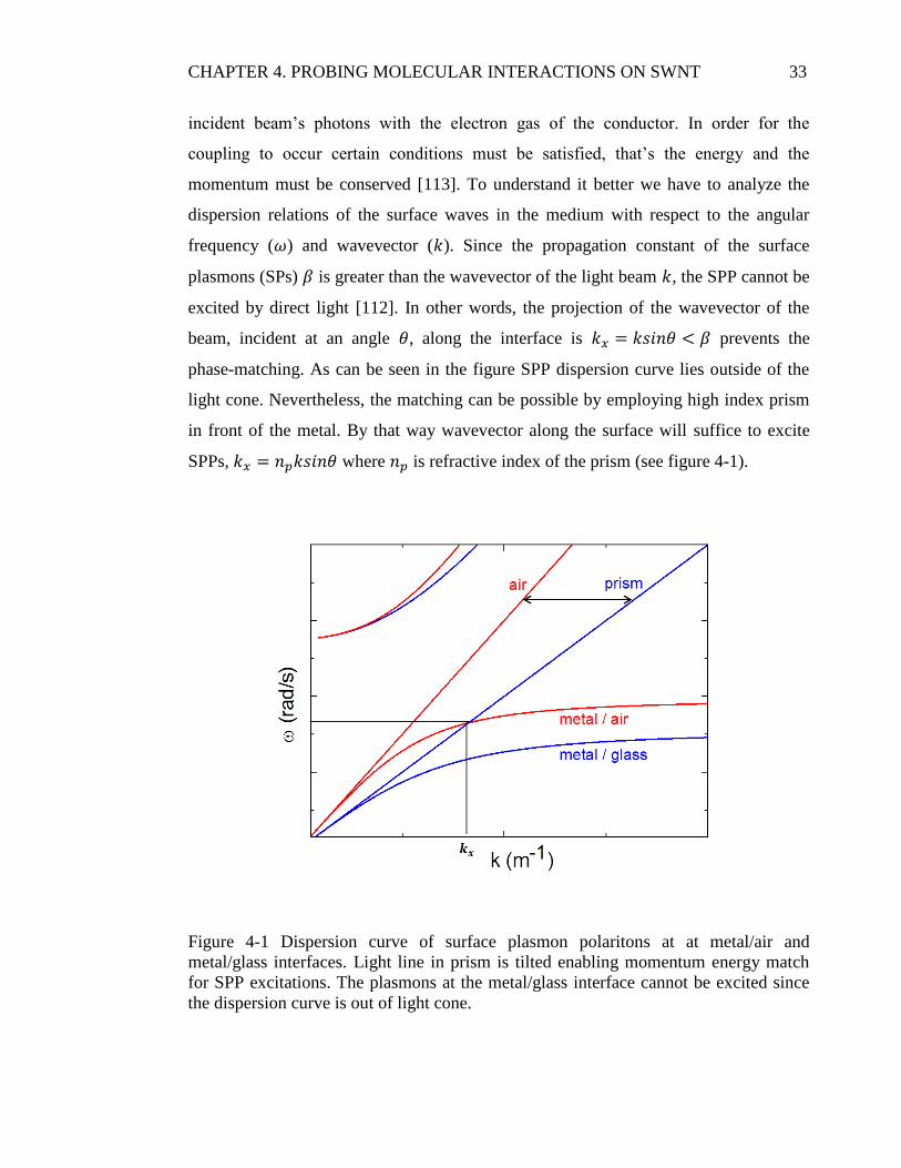
incident beam’s photons with the electron gas of the conductor. In order for the
coupling to occur certain conditions must be satisfied, that’s the energy and the
momentum must be conserved [113]. To understand it better we have to analyze the
dispersion relations of the surface waves in the medium with respect to the angular
frequency ( ) and wavevector ( ). Since the propagation constant of the surface
plasmons (SPs) is greater than the wavevector of the light beam , the SPP cannot be
excited by direct light [112]. In other words, the projection of the wavevector of the
beam, incident at an angle , along the interface is prevents the
phase-matching. As can be seen in the figure SPP dispersion curve lies outside of the
light cone. Nevertheless, the matching can be possible by employing high index prism
in front of the metal. By that way wavevector along the surface will suffice to excite
SPPs, where is refractive index of the prism (see figure 4-1).
Figure 4-1 Dispersion curve of surface plasmon polaritons at at metal/air and
metal/glass interfaces. Light line in prism is tilted enabling momentum energy match
for SPP excitations. The plasmons at the metal/glass interface cannot be excited since
the dispersion curve is out of light cone.

CHAPTER 4. PROBING MOLECULAR INTERACTIONS ON SWNT 34
The dispersion relation (see figure 4-1) is given by,
√
(4.1)
where c is the speed of light, are the dielectric constants of dielectric and
metal respectively. The dispersion curve was plotted for air ( and assuming the
Drude model for electron gas [113]. There are two distinct configurations which
include prism coupler, Kretschmann and Otto, see figure 4-2 [114]. The former one is
most commonly used configuration due to its practicality. It includes thin metal film
evaporated on one surface of high index prism. The photons of the beam falling onto
the interface at angle greater than the critical angle penetrate through the metal and
couple with the surface plasmons. Unlike Kretschmann configuration, the Otto
geometry includes air gap between the prism and metal film. In this configuration, the
beam is totally internally reflected at the prism-air interface creating propagating
evanescent waves which excite surface plasmons at the air-metal interface.

CHAPTER 4. PROBING MOLECULAR INTERACTIONS ON SWNT 35
Figure 4-2 Surface plasmon polariton excitation geometries. a) Kretschmann
configuration b) Otto configuration.

CHAPTER 4. PROBING MOLECULAR INTERACTIONS ON SWNT 36
4.2 Probing Molecular Interactions on SWNT
In this work we integrated surface plasmon resonance (SPR) sensors with networks of
single-walled carbon nanotubes to study interactions between SWNT and organic
molecules. SPR sensors provide surface specific detection schemes with superior
sensitivity. The evanescent field of surface plasmons (SPs) decays exponentially from
the surface with a decay length of a few hundreds of nanometers. Surface specific
detection together with the high sensitivity allows the widespread acceptance of SPR
sensors. Here we implement SPR sensors to probe dynamics of a medium size protein
on SWNT surfaces. SWNT networks with various tube densities were grown by
chemical vapor deposition and then transfer-printed on gold surfaces. To understand
the effects of SWNT on plasmonic properties of the surface, we first measured the
resonance characteristics of SPPs on SWNT functionalized gold surface. As a
demonstration we studied binding dynamics of bovine serum albumin protein on
SWNT network with various tube densities. The sample preparation is demonstrated in
figure 4-3.
Figure 4-3 Transfer printing process of SWNT network grown on SiO2 coated Si
substrates.

CHAPTER 4. PROBING MOLECULAR INTERACTIONS ON SWNT 37
The SWNT networks were grown by catalytic chemical vapor deposition technique
using iron nanoparticles as seeds for the growth. The process starts with coating the
wafers with a 500 nm thick photoresist (Shipley 1805) doped with Fe2Cl3 having
concentration of 1-3 mM. Annealing the photoresist in air results in dispersed iron
oxide nanoparticles on the SiO2 surface. Iron oxide particles are reduced by hydrogen
(300 sccm) as the temperature of the samples reaches to 920 o
C. After reducing the
iron oxide particles, we started the SWNT growth by flowing ethanol vapor in to the
chamber using a carrier flow of 50 sccm Ar and 50 sccm H2 at 920 o
C. After 15
minutes, we terminated the growth and cooled the samples back to the room
temperature under a flow of Ar. The density of SWNT networks was controlled by
changing the concentration of Fe2Cl3 in the photoresist layer. Following the growth, we
transferred SWNTs on metal substrates. Growing SWNT directly on 50 nm gold
surface is not possible because of dewetting of gold layer on SiO2 surface[115]. In
order to solve this problem, we developed a transfer printing process. Fig. 1 shows the
steps of the transfer-printing process of SWNT networks to the gold surface. We first
evaporated 50 nm thick gold film on the SWNT network. The role of the gold layer is
twofold; first it provides mechanical support for SWNT during the transfer process
with low adhesion on SiO2 surface, second, it supports surface plasmon-polaritons. We
applied the gold coated surface on a glass slide coated with UV curable polymer (Epo-
Tek, OG146). A 5-minute exposure of UV light cures the polymer layer and sticks the
gold-SWNT layer to the cured polymer surface. The SWNT networks on gold surface
are achieved by mechanically removing the substrate with a razorblade.
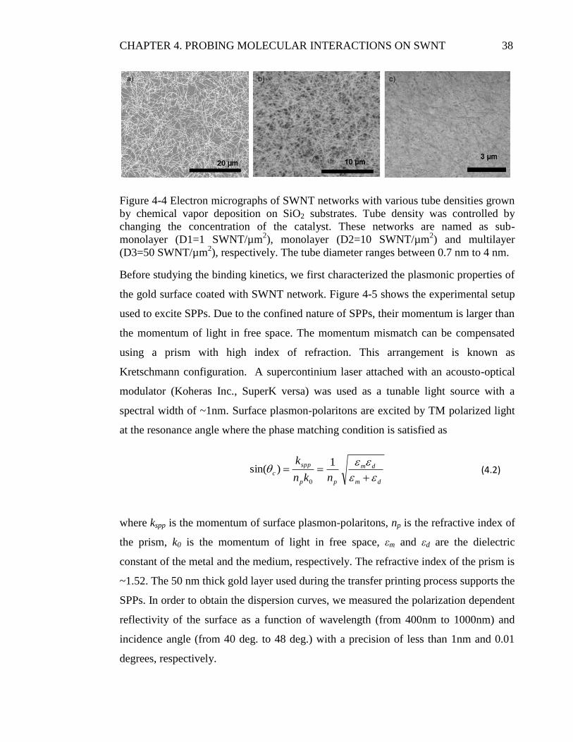
Figure 4-4 shows the scanning electron micrographs of SWNT networks with various
tube densities on SiO2 substrates. The tube density was controlled by changing the
catalyst concentration. The surface coverage of the SWNT networks ranges from
submonolayer (~5% coverage) to multilayer. We named the three representative tube
density as D1 (submonolayer), D2 (monolayer) and D3 (multilayer). The tube densities
for D1, D2 and D3 are ~1 SWNT/µm2 ~10 SWNT/µm
2 and ~50 SWNT/µm
2,
respectively. The carbon nanotubes are primarily single-walled with tube diameters
from 0.7 nm to 4 nm.
CHAPTER 4. PROBING MOLECULAR INTERACTIONS ON SWNT 38
Figure 4-4 Electron micrographs of SWNT networks with various tube densities grown
by chemical vapor deposition on SiO2 substrates. Tube density was controlled by
changing the concentration of the catalyst. These networks are named as sub-
monolayer (D1=1 SWNT/µm2), monolayer (D2=10 SWNT/µm
2) and multilayer
(D3=50 SWNT/µm2), respectively. The tube diameter ranges between 0.7 nm to 4 nm.
Before studying the binding kinetics, we first characterized the plasmonic properties of
the gold surface coated with SWNT network. Figure 4-5 shows the experimental setup
used to excite SPPs. Due to the confined nature of SPPs, their momentum is larger than
the momentum of light in free space. The momentum mismatch can be compensated
using a prism with high index of refraction. This arrangement is known as
Kretschmann configuration. A supercontinium laser attached with an acousto-optical
modulator (Koheras Inc., SuperK versa) was used as a tunable light source with a
spectral width of ~1nm. Surface plasmon-polaritons are excited by TM polarized light
at the resonance angle where the phase matching condition is satisfied as
dm
dm
pp
spp
cnkn
k
1)sin(
0
(4.2)
where kspp is the momentum of surface plasmon-polaritons, np is the refractive index of
the prism, k0 is the momentum of light in free space, εm and εd are the dielectric
constant of the metal and the medium, respectively. The refractive index of the prism is
~1.52. The 50 nm thick gold layer used during the transfer printing process supports the
SPPs. In order to obtain the dispersion curves, we measured the polarization dependent
reflectivity of the surface as a function of wavelength (from 400nm to 1000nm) and
incidence angle (from 40 deg. to 48 deg.) with a precision of less than 1nm and 0.01
degrees, respectively.

CHAPTER 4. PROBING MOLECULAR INTERACTIONS ON SWNT 39
Figure 4-6 shows the reflectivity maps from the SWNT coated gold surfaces as a
function of excitation wavelength and incidence angle. The wavelength scans the
energy of the exited SPPs and the angle defines the momentum. The maps were
obtained from the TM polarized reflection spectra. When the resonance condition (eqn.
4.2) is satisfied, the reflectivity goes to a minimum value. The resonance wavelength is
obtained from the minimum value. We observed that as the surface coverage increases,
the resonance wavelength red-shifts and the spectral width of the surface plasmon
resonance gets broader, which is likely because of additional optical losses (scattering
losses) associated with the high density of SWNT networks.
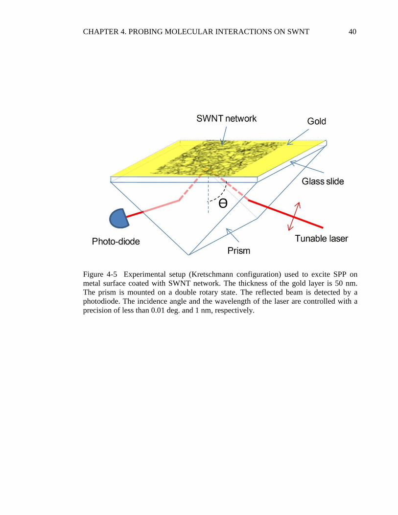
CHAPTER 4. PROBING MOLECULAR INTERACTIONS ON SWNT 40
Figure 4-5 Experimental setup (Kretschmann configuration) used to excite SPP on
metal surface coated with SWNT network. The thickness of the gold layer is 50 nm.
The prism is mounted on a double rotary state. The reflected beam is detected by a
photodiode. The incidence angle and the wavelength of the laser are controlled with a
precision of less than 0.01 deg. and 1 nm, respectively.

CHAPTER 4. PROBING MOLECULAR INTERACTIONS ON SWNT 41
Figure 4-6 The reflectivity maps (angular dispersion curves) from the SWNT coated
gold surface as a function of incidence angle and the excitation wavelength. The light
source is TM polarized. As the density of SWNTs network increases, the effective
index of the surface plasmon-polaritons increases resulting in a red shift in the plasmon
resonance wavelength. The color map shows the scale for the reflectivity.

CHAPTER 4. PROBING MOLECULAR INTERACTIONS ON SWNT 42
The characteristic surface plasmon absorption dip can be seen not only by scanning the
wavelength of the excitation, but also it can be obtained by scanning the incidence
angle with monochromatic excitation. Figure 4-7 summarizes the change in the
reflection spectra with increasing tube density. Figure 4-7a shows the reflection spectra
of the surface recorded at an incidence angle of 44 deg. There are two resonances; the
one that is at around 470 nm is due to the bulk plasmon absorption, the second
resonance at around 605 nm is due to the surface plasmon-polaritons. The bulk
plasmon absorption is independent of the surface coverage. Angular dependence of the
reflectivity from the surfaces is shown in figure 4-7b. The resonance angle increases
with increasing tube density. Figure 4-7c and 4-7d show the change of resonance
wavelength and resonance angle as a function of tube density, respectively.

CHAPTER 4. PROBING MOLECULAR INTERACTIONS ON SWNT 43
Figure 4-7 (a) Reflection spectra from the gold surface for various tube densities. The
incidence angle is 44 deg. There are two resonances in the reflectivity spectra; bulk
plasmon resonance of around 450 nm and surface plasmon resonance of around 600
nm. (b) Reflectivity of the surface as a function of incidence angle for various surface
coverage. (c,d) Dependence of surface plasmon resonance wavelength and angle on the
surface coverage of SWNT networks, respectively.

CHAPTER 4. PROBING MOLECULAR INTERACTIONS ON SWNT 44
The gold surface functionalized with SWNT network provides us a unique platform to
probe binding interaction between SWNT surface and organic molecules. As a proof of
principle, we studied nonspecific binding of a bovine serum albumin (BSA) protein on
SWNT surface In order to probe binding interactions of proteins on SWNT network,
we integrated the SPR sensor with a microfluidic device. Figure 4-8a shows the
fabrication steps the device. The device consists of an elastomeric flow chamber sealed
on the SWNT functionalize gold surface. For efficient coupling of SPP, the thickness
of the gold layer is chosen to be 50 nm. A TM polarized diode laser (λ=635 nm) and a
prism with a high index of refraction (BK7, np=1.78) are used to excite SPPs. The
reflectivity as a function of incidence angle is given in Figure 4-8b. The SPR angle is at
57 deg. After setting the incidence angle to the resonance angle, we first run DI water
through the flow chamber for 5 min. When the SPR signal was stabilized, we started
the flow of 100 nM BSA solution and recorded the SPR signal for 30 minutes. We
repeated the same procedure for a bare gold surface and gold surfaces coated with three
different SWNT networks shown in figure 4-4. The time traces of SPR signal for
binding interaction of BSA on the various surfaces are shown in figure 4-8c. After the
SPR signal saturated, we washed the surface with DI water. We did not observe any
change in SPR signal, which indicates that BSA is kinetically stable on SWNT surface.
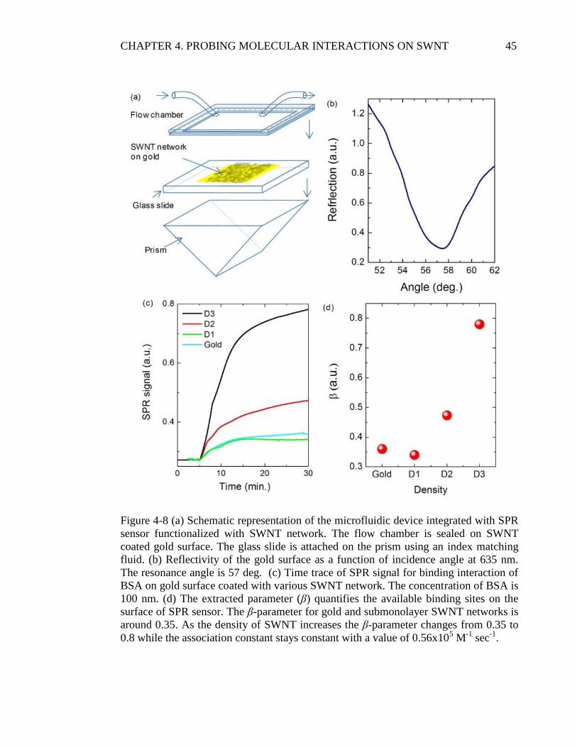
CHAPTER 4. PROBING MOLECULAR INTERACTIONS ON SWNT 45
Figure 4-8 (a) Schematic representation of the microfluidic device integrated with SPR
sensor functionalized with SWNT network. The flow chamber is sealed on SWNT
coated gold surface. The glass slide is attached on the prism using an index matching
fluid. (b) Reflectivity of the gold surface as a function of incidence angle at 635 nm.
The resonance angle is 57 deg. (c) Time trace of SPR signal for binding interaction of
BSA on gold surface coated with various SWNT network. The concentration of BSA is
100 nm. (d) The extracted parameter (β) quantifies the available binding sites on the
surface of SPR sensor. The β-parameter for gold and submonolayer SWNT networks is
around 0.35. As the density of SWNT increases the β-parameter changes from 0.35 to
0.8 while the association constant stays constant with a value of 0.56x10⁵ M
-1 sec
-1.

CHAPTER 4. PROBING MOLECULAR INTERACTIONS ON SWNT 46
To understand the nonspecific binding of BSA on SWNT network, we used a first-
order pseudo-kinetic equation. Since we employed a flow cell the number of molecules
in the medium is much higher than the available binding sides on the surface. The
pseudo-kinetic equation can be written as
AkACkdt
dAda )( (4.3)
where A is the concentration of molecules binding to the surface, ka is the association
rate constant, β is the concentration of free binding sides, and kd is the dissociation rate
constant. Since we did not observe any disassociation from the surface the value of kd
is zero. With these conditions, the solution of the kinetic equation is
)1()(AtkaetC
(4.4)
In the linear regime of the reflection spectrum, the SPR signal is proportional with the
concentration of molecules binding to the surface. We obtained β and ka values from
the least squares fitting of the time trace of SPR signal for various SWNT networks.
Figure 4-8d shows that the extracted values of β which quantifies the concentration of
free binding sides. The concentration of free binding sides increases with the tube
density while the association constant stays constant with a value of 0.56x10⁵ M
-1 sec
-1.
As a conclusion, we present a SPR sensor to probe binding dynamics of organic
molecules on SWNT surfaces. SWNT networks with various tube densities were grown
by chemical vapor deposition and then transfer-printed on gold surfaces. We
characterized the plasmonic properties of SWNT coated gold surfaces. As a
demonstration we studied binding dynamics of bovine serum albumin protein on
SWNT networks with various tube densities. We observed that the concentration of
free binding sides increases with the tube density while the association constant stays
constant with a value of 0.56x10⁵ M
-1 sec
-1. We anticipate that SWNT functionalized
SPR sensors could provide a sensitive means for probing adsorption of organic
molecules on surfaces of SWNT.
47
Chapter 5
5. Probing Interfacial Processes on
Graphene
This chapter presents a method for probing interfacial processes on graphene surface
using mass detection. Graphene layers were synthesized by chemical vapor deposition
on copper foils and transfer-printed on a quartz crystal microbalance (QCM). Probing
the mechanical resonance of the QCM, we were able to measure mass density of single
layer graphene. We extended the developed technique to probe binding dynamics of
proteins on graphene surface. Furthermore, we monitored oxidation of graphene
surface under oxygen plasma by tracing the changes of interfacial mass of the graphene
layer.
5.1 Interfacial mass detection with piezoelectric transducers
Ward and Buttry in their paper [116] reviewed basic properties, practical methods and
applications of mass-sensing piezoelectric crystal sensors. As discussed, a principle
phenomenon behind the mass-sensing transducers is converse piezoelectric effect,
which is basically the induced stress on piezoelectric material by applied electric field.
In fact, if AC voltage is applied across piezoelectric crystal, it causes an alternating
strain field which in turn creates acoustic standing waves in quartz crystals. These
crystals prefer to oscillate at resonance frequency with high quality factor Q, which
make them ideal oscillators [117]. Here the symmetry of the crystal plays crucial role
in electromechanical stresses enabling various modes of couplings. Such modes are

CHAPTER 5. PROBING INTERFACIAL PROCESSES ON GRAPHENE 48
consequent for diverse class of acoustic waves, propagations, and particle
displacements. For instance, electric field across AT-cut quartz causes shear vibrations,
see figure. Furthermore, thickness shear mode specified by AT-cut crystal is used to
describe mass-sensing. The shear motion is bound by two electrodes and analogous to
standing wave with length . Hence the fundamental frequency of the string is equal to
(
)
where is the tension on the string, is the mass per unit length, and is
the length of the string, and dependent on the mass. Similarly, AT-cut quartz possesses
fundamental frequency as (
)
where is the thickness, is the shear
modulus and is the density of the quartz crystal. An increase in the thickness of
quartz crystal results in the decrease of fundamental frequency. Sauerbrey
demonstrated the mass-frequency dependence in terms of foreign layer depositions on
thickness shear mode quartz crystal. The assumption lies in that the deposited foreign
mass becomes an extension of the quartz crystal, and hence frequency change can be
expressed as:
(5.1)
The linear relationship of the frequency shift and the variation of mass are summarized
in Sauerbrey’s equation.
√
(5.2)
where f0 is the resonant frequency of the fundamental mode of the quartz crystal. For
AT cut, 5MHz quartz crystal, the mass density is =2.648 g cm-3
and the shear
modulus is µq=2.947x10¹¹
g cm-1
s-2
. The assumption behind Sauerbrey’s equation is
that the mass distribution is uniform and cover entire electrode region of the quartz. It
is significant due to the variations in the sensitivities as the shear mode amplitude drops
away from the center to the edges [118]. The liquid contact mode is clear in quartz
crystal microbalance devices as the particles move parallel to the surface. Although, the
CHAPTER 5. PROBING INTERFACIAL PROCESSES ON GRAPHENE 49
density and viscosity of the liquid do affect the operating frequency of the quartz
crystal, the mass sensitivity stays unaffected in the environment of the liquid. Ward and
Buttry also claimed that one disadvantage is the QCM approach cannot distinguish
changes caused by either mass depositions or viscoelasticity of thin films or liquids.
Nevertheless, this can be overcome using impedance or network analyzer and
measuring Q factor which defines width of resonance curve and energy dissipated
during oscillations. Since Q is inversely proportional to any viscous effect, the
measurement reveals changes in mass. Moreover, QCM transducers are able to track
the real time kinetic processes in the media. The primary factor of the resolution is the
time that takes to reach equilibrium between mass deposits and device. This limit relies
on the Q and given by [119]. For example, the AT-cut quartz has Q values as
high as for vapor and nonviscous loads and responds rapidly while for
liquids Q value is low ( ) hence time resolution is around milliseconds.
Nonetheless, even such resolutions are sufficient to time-trace the kinetic processes,
nucleation, growth, and dissolution [120].
5.2 Integration of graphene with QCM
To integrate graphene with QCM, we developed a transfer-printing process. We used
AT-cut, α-quartz crystal (331µm thick) with a mechanical response frequency of 5
MHz. The crystals are 1 inch in diameter with circular chrome/gold electrodes
patterned on both sides. The exposed area of the front electrode is around 1.37 cm2.
The area of the graphene layer is 0.64±0.05 cm2. Figure 5-1 illustrates the steps of the
transfer printing process. The graphene layers were synthesized on copper foils by
chemical vapor deposition[106]. The copper foils were placed in a quartz chamber and
heated to 1050 oC under flow of hydrogen gas. To reduce the oxide layer, the samples
were annealed for 30 min at 1050 oC. After the annealing process, methane gas with a
rate of flow of 7 sccm was sent to the chamber for 20 min. The chamber pressure was
kept at 200 mTorr during the growth. The growth was terminated by stopping the flow
of methane gas and the chamber was cooled back to the room temperature. The
graphene coated copper foils were spin coated with a photoresist (PR, AZ5214) with a
thickness of 1.4 µm. A flat elastomeric stamp (PDMS) was placed on the PR layer and

CHAPTER 5. PROBING INTERFACIAL PROCESSES ON GRAPHENE 50
the copper foil was etched by 1 M iron chloride solution. After the etching, the PR with
graphene layer remains on the PDMS stamp. The stamp was applied on the QCM and
heated to 100 oC to release the graphene-PR layer. Removing the PR layer in acetone
provides large area graphene on the surface of QCM.
Figure 5-1 Transfer-printing process of graphene on the front electrode of a quartz
crystal microbalance.
To obtain the resonance characteristics of the QCM, we measured scattering
parameters (S-parameters, S11) of QCM using two-port vector network analyzer (VNA,
HP 8753D). S-parameters can elucidate the electromechanical properties of QCM and
as well as the interaction of the surrounding medium. Figure 5-2a shows the
schematics of the experimental setup. One port of the VNA is connected to the QCM
mounted on a crystal holder with a BNC connector. We measured S-parameters for a
frequency range of 1 kHz around the resonance frequency of 5MHz. Figure 5-2b shows
the phase and magnitude of measured S11. S11 shows a clear resonance behavior due to
the mechanical resonance of the QCM. At the resonance frequency the magnitude of
S11 is at a minimum since the total impedance attains its minimum value at the
resonance frequency. S11 at the resonance is 3 dB less than the off-resonance value. A

CHAPTER 5. PROBING INTERFACIAL PROCESSES ON GRAPHENE 51
steep phase change at the resonance frequency is also a characteristic behavior of an
electromechanical resonator. The resonance of quartz crystal has very narrow
bandwidth which makes them ideal for frequency measurements. The resonance
frequency and the quality factor of the blank QCM are 5,007,323.4 Hz and 22600,
respectively. After measuring the S-parameters of the blank QCM, we transfer-printed
single layer graphene and measured the S-parameters of graphene coated QCM. The
area of transferred graphene is 0.64 cm2 which is smaller than the area of the front
electrode, 1.37 cm2. The dot lines in Figure 5-2b show the S-parameters of graphene-
coated QCM. After the transfer process, the resonance frequency decreases owing to
the mass uptake. We observed a frequency change of 20.5 Hz after transferring the
graphene layer. The change in the resonance frequency is proportional with the
additional mass on QCM which consist of mass of the graphene layer and organic
residue due to the transfer process.

CHAPTER 5. PROBING INTERFACIAL PROCESSES ON GRAPHENE 52
Figure 5-2 (a) Experimental set-up used for probing resonance characteristic of the
QCM. A two-port network analyzer is used to measure scattering parameters. (b)
Magnitude (blue lines) and phase (red lines) of the measured scattering parameter S11
of the port-1, as a function of frequency for blank (solid line) and graphene coated
QCM (dot line). The resonance frequency is 5,007,323.4 Hz. The Q-factor of the
resonator is around 22600. After coating the surface of QCM with 0.64 cm2
graphene,
we observed around 20 Hz shift in the resonance frequency.

CHAPTER 5. PROBING INTERFACIAL PROCESSES ON GRAPHENE 53
By repeating the transfer-printing of graphene, we were able to obtain multilayer
graphene films which allow us to measure the mass density of graphene. Figure 5-3
shows the scattering parameters for a QCM coated with multilayer graphene. The
multilayer graphene films were obtained by a sequential transfer printing process. After
each transfer process, we measured the scattering parameters. Figures 5-3a and 5-3b
show the magnitude and phase of QCM coated with multilayer graphene films. We
observed a linear change in the resonance frequency. The scattered plot in Fig3c shows
the change of resonance frequency with the layer number. The red line shows the
curve obtained by the linear least squares fitting. The slope of the fitting curve provides
the interfacial mass change after transfer-printing process. The frequency change of 26
±2 Hz for each graphene layer is obtained from the fitting curve. It is known that
polymer-assistant-transfer-printing process carries some degree of organic residues. We
also performed some controlled experiment to quantify the amount of organic residue
carried on the QCM.
To quantify the frequency change and mass uptake, we calibrated the QCM by a known
amount of mass. A uniform gold film with a thickness of 20nm-measured by an atomic
force microscope- was evaporated on QCM with the same area as the graphene sheets.
We measured a shift of 4.80 kHz in resonant frequency. The density of the evaporated
gold thin film is 16 g/cm-3
[121] which corresponds to a mass uptake of 20.5 µg. Since
the sensitivity of QCM decreases with the radial distance, we keep the area of the film
constant during the calibration. For an exposed area of 0.64 cm2, the calibration factor
is 4.26 ng/Hz. For each graphene layer we obtained 26 Hz frequency shift
corresponding a mass uptake of 114 ng. This value includes the mass of both graphene
and organic residue. To elucidate the mass of residue, we performed the similar transfer
process without growing graphene on copper foils. The observed frequency shift for
each transfer process is 8.3 Hz corresponds to a mass uptake of 35ng. After subtracting
the mass of residues from the measured mass and normalizing by the area, we estimate
the mass density of graphene as 123 ng/cm2. This value is 35% larger than the
theoretical value of 79 ng/cm2 calculated from the mass density of bulk graphite. This
variation is likely because of chemical vapor deposition process which produces

CHAPTER 5. PROBING INTERFACIAL PROCESSES ON GRAPHENE 54
polycrystalline graphene with partial multilayer regions and underestimated mass of
organic residues on the graphene or errors in the area of the transferred graphene.
There are also other sources of errors related with the calibration procedure such as the
thickness and mass density of gold film used for the calibration. We also observed a
slight change of band width of QCM likely because of additional interfacial friction
between the graphene layers. Figure 5-3d shows the bandwidth of the QCM as a
function of graphene layers.
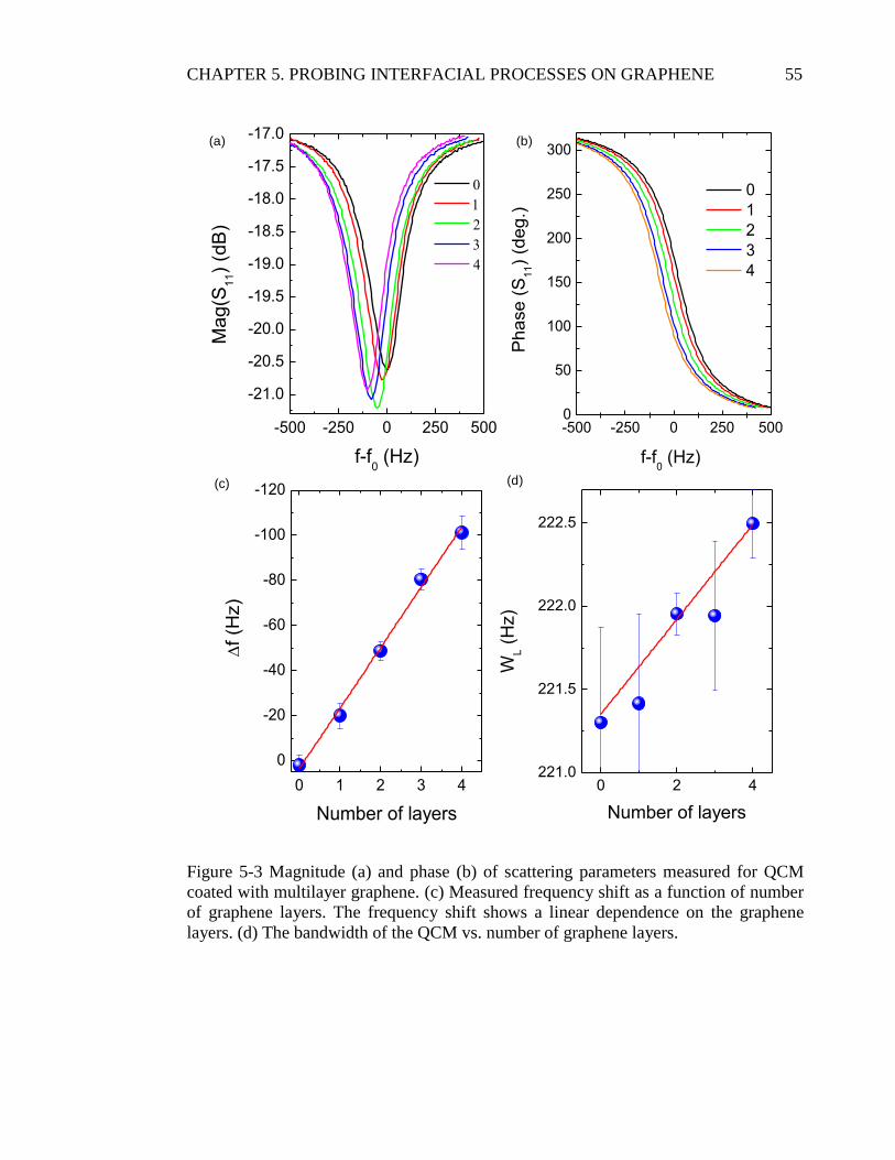
CHAPTER 5. PROBING INTERFACIAL PROCESSES ON GRAPHENE 55
Figure 5-3 Magnitude (a) and phase (b) of scattering parameters measured for QCM
coated with multilayer graphene. (c) Measured frequency shift as a function of number
of graphene layers. The frequency shift shows a linear dependence on the graphene
layers. (d) The bandwidth of the QCM vs. number of graphene layers.
-500 -250 0 250 500
-21.0
-20.5
-20.0
-19.5
-19.0
-18.5
-18.0
-17.5
-17.0
Mag(S
11)
(dB
)
f-f0 (Hz)
0 2 4221.0
221.5
222.0
222.5
WL (
Hz)
Number of layers
-500 -250 0 250 5000
50
100
150
200
250
300
0
1
2
3
4
Phase (
S11)
(deg.)
f-f0 (Hz)
(b)(a)
0 1 2 3 4
0
-20
-40
-60
-80
-100
-120
f
(Hz)
Number of layers
(d)(c)

CHAPTER 5. PROBING INTERFACIAL PROCESSES ON GRAPHENE 56
QCM sensors can work in liquid media as well. Integrating the QCM sensor with a
flow chamber, we monitored the binding dynamics of proteins on graphene surface
from an aqueous solution. We would like to demonstrate that integration of graphene
with QCM sensors can be used to probe binding kinetics of organic molecules on
graphene surface by means of change of interfacial mass. Figure 5-4a shows schematic
representation of the experimental setup used to probe the resonance frequency of the
QCM sensor in real time. Quartz crystal is placed in the feedback loop of an oscillator.
The time trace of the resonance frequency was monitored by means of a frequency
counter. We used a quartz crystal microbalance (Stanford Research, QCM200)
integrated with a flow cell. The kinetic parameters of the nonspecific binding on a
surface can be extracted from the time trace of the resonance frequency which provides
the interfacial mass change. We used 100 nM of Bovine serum albumin (BSA) - a
medium size protein-to study nonspecific binding on the surface of bare gold electrode
and graphene coated gold electrode. From the time trace of the frequency change, we
can obtain the time constant of the binding kinetics. The time constants, obtained by
fitting the time trace data, are 390 sec and 30 sec, for bare QCM and graphene coated
QCM, respectively. From the measured the time constants, we can estimate the
association constants of BSA on bare gold surface and graphene coated gold surface as
0.26 M-1
sec-1
and 3.3 M-1
sec-1
, respectively. There is a significant increase in the
association constant likely because of hydrophobic nature of the graphene surface.

CHAPTER 5. PROBING INTERFACIAL PROCESSES ON GRAPHENE 57
Figure 5-4(a) Schematics of the experimental setup used to probe the time trace of the
resonance frequency of the QCM. (b) Overlaid time trace of resonance frequency
indicating the binding kinetics of Bovine serum albumin (BSA) proteins on the bare
QCM surface and graphene coated QCM surface. The concentration of BSA is 100nM.
250 500 750 10000
-20
-40
-60
-80
-100
Fre
que
ncy s
hift
(Hz)
Time (sec)
QCM
Graphene coated QCM
OscillatorFrequency
counter
(a)
QCM
(b)

CHAPTER 5. PROBING INTERFACIAL PROCESSES ON GRAPHENE 58
Mass detection can also be used for monitoring chemical reactions on graphene
surfaces. We would like to trace oxidation of the graphene surface by monitoring the
interfacial mass change and correlate the mass change with Raman spectra. The
graphene structure undergoes chemical variations as it is exposed to mild oxygen
plasma. After transfer-printing the graphene layers on a QCM, we exposed the surface
to mild oxygen plasma in a reactive ion etching chamber. After each short exposure
time, we measured the change in the resonance frequency of the QCM. Figure 5-5
exhibits the change of the resonant frequency and correlated mass uptake associated
with the oxidation of the graphene surface. We performed the exposure of plasma until
complete etching of the graphene layer. To correlate the mass uptake and the crystal
structure of the graphene layer, we measured the Raman spectra of graphene after each
exposure. Figure 5-5 (b) shows the recorded Raman spectra for various exposure times.
We observed three different regimes, for the first 10 sec. interfacial mass increases by
93 ng/cm2. This mass uptake is likely due to the oxidation of the graphene layer. This
oxidation can also be seen from the Raman spectra. The increase of the intensity of the
D-band (1950 cm-1
) confirms the formation of sp bonds and associated lattice
distortion. The decrease in the intensity of 2D-band (2700 cm-1
) shows deformation of
the crystal structure of graphene. After 15 sec. of expose we observed a decrease in the
interfacial mass. This decrease could be because of CO2 release which is expected for
early stage of graphene oxidation. As we further increase the exposure time, we
observed complete removal of the graphene layer. This step could include physical
removing of small graphene/graphene oxide flakes because of bombarding of the
surface by energetic oxygen atoms. Correlating the interfacial mass change and Raman
spectra could provide more inside for understanding the interfacial reaction of graphene
surface.

CHAPTER 5. PROBING INTERFACIAL PROCESSES ON GRAPHENE 59
Figure 5-5 Probing oxidation of graphene by mass detection. (a) Change of the
resonant frequency and associated mass uptake of graphene exposed to mild oxygen
plasma. (b) Raman spectra of graphene with various exposure times. (c-f) Mass uptake
of graphene and correlated with Raman intensity for D, G and 2D bands.
1000 1500 2000 2500 3000
60
80
100
120
140
160
180
200
Inte
nsity (
a.u
.)
Wavenumber (cm-1)
0 sec.
5 sec.
10 sec.
15 sec.
0 5 10 150
20
40
8
12
16
0
10
20
30
-20
0
20
40
60
80
0 5 10 15
I D (
a.u
)I
2D(a
.u)
I G (
a.u
)Exposure time (sec)
Ma
ss u
pta
ke
(c)
(d)
(e)
(f)
0 15 30 45 60 75 90 390-20
-15
-10
-5
0
5
10
15
20
25
30
Fre
quency s
hift (H
z)
Exposure time (sec.)
100
50
0
-50
-100
-150
Mass u
pta
ke (
ng/c
m2)
(a)
(b)

60
Chapter 6
6. Summary and future work
In this thesis, we used SWNT networks and single layer graphene as model materials to
understand interfacial process on graphitic carbon surface. In the first part of the thesis,
we synthesized SWNT networks by chemical vapor deposition and transfer-printed on
gold surfaces. We studied the excitation of surface plasmon-polaritons on nanotube
coated gold surfaces with sub-monolayer, monolayer, and multilayer surface coverage.
Integrating the fabricated sensor with a microfluidic device, we were able to obtain
binding dynamics of a bovine serum albumin (BSA) protein on SWNT networks with
various tube densities. The results reveal the kinetic parameters for nonspecific binding
of BSA on SWNT surface for various tube densities. In the second part of the thesis,
graphene layers were synthesized by chemical vapor deposition on copper foils and
transfer-printed on a quartz crystal microbalance (QCM). Probing the mechanical
resonance of the QCM, we were able to measure mass density of single layer graphene.
We extended the developed technique to probe binding dynamics of proteins on
graphene surface. We obtained association constant of nonspecific binding of BSA on
graphene surface from an aqueous solution. The presence of graphene layer increases
the nonspecific binding likely because of the hydrophobic nature of graphitic carbon.
Furthermore, we monitored oxidation of graphene surface under oxygen plasma by
tracing the changes of interfacial mass of the graphene layer. During the oxidation of
graphene, by monitoring the mass change and change of Raman spectra, we observed
three regimes, (1) formation of graphene oxide which increases the interfacial mass, (2)
release of CO2 and (3) removal of small graphene/graphene oxide flakes.

CHAPTER 6. SUMMARY AND FUTURE WORK 61
Further studies must be done to fully understand the adsorption of organic molecules
on carbon surface. In this study we provide a proof-of-principle demonstration of two
different methods based on optical and mass detection. We would like continue this
work by studying adsorption of small molecules on SWNT and graphene surface from
gas phase and aqueous solution. We anticipate that with the help of these techniques,
we can understand the fundamental interaction on carbon surface at the molecular
level.

62
7. Bibliography:
[1] S. Iijima, "Helical Microtubules of Graphitic Carbon," Nature, vol. 354, pp. 56-
58, Nov 7 1991.
[2] A. K. Geim and K. S. Novoselov, "The rise of graphene," Nature Materials,
vol. 6, pp. 183-191, 2007.
[3] T. Masciangioli and W. X. Zhang, "Environmental technologies at the
nanoscale," Environ Sci Technol, vol. 37, pp. 102a-108a, Mar 1 2003.
[4] D. Tasis, N. Tagmatarchis, A. Bianco, and M. Prato, "Chemistry of carbon
nanotubes," Chemical Reviews, vol. 106, pp. 1105-1136, Mar 2006.
[5] W. R. Yang, K. R. Ratinac, S. P. Ringer, P. Thordarson, J. J. Gooding, and F.
Braet, "Carbon Nanomaterials in Biosensors: Should You Use Nanotubes or
Graphene?," Angewandte Chemie-International Edition, vol. 49, pp. 2114-
2138, 2010.
[6] C. Wang, A. Badmaev, A. Jooyaie, M. Q. Bao, K. L. Wang, K. Galatsis, and C.
W. Zhou, "Radio Frequency and Linearity Performance of Transistors Using
High-Purity Semiconducting Carbon Nanotubes," Acs Nano, vol. 5, pp. 4169-
4176, May 2011.
[7] E. Pince and C. Kocabas, "Investigation of high frequency performance limit of
graphene field effect transistors," Applied Physics Letters, vol. 97, Oct 25 2010.
[8] Y. M. Lin, A. Valdes-Garcia, S. J. Han, D. B. Farmer, I. Meric, Y. N. Sun, Y.
Q. Wu, C. Dimitrakopoulos, A. Grill, P. Avouris, and K. A. Jenkins, "Wafer-
Scale Graphene Integrated Circuit," Science, vol. 332, pp. 1294-1297, Jun 10
2011.

BIBLIOGRAPHY 63
[9] C. Kocabas, H. S. Kim, T. Banks, J. A. Rogers, A. A. Pesetski, J. E.
Baumgardner, S. V. Krishnaswamy, and H. Zhang, "Radio frequency analog
electronics based on carbon nanotube transistors," Proc Natl Acad Sci U S A,
vol. 105, pp. 1405-9, Feb 5 2008.
[10] S. J. Kang, C. Kocabas, T. Ozel, M. Shim, N. Pimparkar, M. A. Alam, S. V.
Rotkin, and J. A. Rogers, "High-performance electronics using dense, perfectly
aligned arrays of single-walled carbon nanotubes," Nat Nanotechnol, vol. 2, pp.
230-6, Apr 2007.
[11] C. Rutherglen, D. Jain, and P. Burke, "Nanotube electronics for radiofrequency
applications," Nat Nanotechnol, vol. 4, pp. 811-9, Dec 2009.
[12] J. P. Hill, W. Jin, A. Kosaka, T. Fukushima, H. Ichihara, T. Shimomura, K. Ito,
T. Hashizume, N. Ishii, and T. Aida, "Self-assembled hexa-peri-
hexabenzocoronene graphitic nanotube," Science, vol. 304, pp. 1481-3, Jun 4
2004.
[13] Y. Zhao and D. G. Truhlar, "Size-selective supramolecular chemistry in a
hydrocarbon nanoring," J Am Chem Soc, vol. 129, pp. 8440-+, Jul 11 2007.
[14] S. Grimme, J. Antony, T. Schwabe, and C. Muck-Lichtenfeld, "Density
functional theory with dispersion corrections for supramolecular structures,
aggregates, and complexes of (bio)organic molecules," Organic &
Biomolecular Chemistry, vol. 5, pp. 741-758, 2007.
[15] J. Kong, N. R. Franklin, C. W. Zhou, M. G. Chapline, S. Peng, K. J. Cho, and
H. J. Dai, "Nanotube molecular wires as chemical sensors," Science, vol. 287,
pp. 622-625, Jan 28 2000.
[16] B. L. Allen, P. D. Kichambare, and A. Star, "Carbon nanotube field-effect-
transistor-based biosensors," Advanced Materials, vol. 19, pp. 1439-1451, Jun 4
2007.
[17] O. Salihoglu, S. Balci, and C. Kocabas, "Plasmon-polaritons on graphene-metal
surface and their use in biosensors," Applied Physics Letters, vol. 100, May 21
2012.
[18] O. Gulseren, T. Yildirim, and S. Ciraci, "Tunable adsorption on carbon
nanotubes," Phys Rev Lett, vol. 87, p. 116802, Sep 10 2001.

BIBLIOGRAPHY 64
[19] E. Durgun, S. Dag, V. M. K. Bagci, O. Gulseren, T. Yildirim, and S. Ciraci,
"Systematic study of adsorption of single atoms on a carbon nanotube,"
Physical Review B, vol. 67, May 15 2003.
[20] E. Durgun, S. Dag, S. Ciraci, and O. Gulseren, "Energetics and electronic
structures of individual atoms adsorbed on carbon nanotubes," Journal of
Physical Chemistry B, vol. 108, pp. 575-582, Jan 15 2004.
[21] P. A. Denis and F. Iribarne, "Thiophene adsorption on Single Wall Carbon
Nanotubes and graphene," Journal of Molecular Structure-Theochem, vol. 957,
pp. 114-119, Oct 15 2010.
[22] S. B. Fagan, A. G. Souza, J. O. G. Lima, J. Mendes, O. P. Ferreira, I. O. Mazali,
O. L. Alves, and M. S. Dresselhaus, "1,2-dichlorobenzene interacting with
carbon nanotubes," Nano Letters, vol. 4, pp. 1285-1288, Jul 2004.
[23] L. L. Wang, D. Q. Zhu, L. Duan, and W. Chen, "Adsorption of single-ringed N-
and S-heterocyclic aromatics on carbon nanotubes," Carbon, vol. 48, pp. 3906-
3915, Nov 2010.
[24] B. Pan and B. S. Xing, "Adsorption Mechanisms of Organic Chemicals on
Carbon Nanotubes," Environ Sci Technol, vol. 42, pp. 9005-9013, Dec 15 2008.
[25] K. Yang, X. L. Wang, L. Z. Zhu, and B. S. Xing, "Competitive sorption of
pyrene, phenanthrene, and naphthalene on multiwalled carbon nanotubes,"
Environ Sci Technol, vol. 40, pp. 5804-5810, Sep 15 2006.
[26] E. S. Alldredge, S. C. Badescu, N. Bajwa, F. K. Perkins, E. S. Snow, T. L.
Reinecke, J. L. Passmore, and Y. L. Chang, "Adsorption of linear chain
molecules on carbon nanotubes," Physical Review B, vol. 78, Oct 2008.
[27] K. Yang, X. Wang, L. Zhu, and B. Xing, "Competitive sorption of pyrene,
phenanthrene, and naphthalene on multiwalled carbon nanotubes," Environ Sci
Technol, vol. 40, pp. 5804-10, Sep 15 2006.
[28] S. Debnath, Q. H. Cheng, T. G. Hedderman, and H. J. Byrne, "Comparative
Study of the Interaction of Different Polycyclic Aromatic Hydrocarbons on
Different Types of Single-Walled Carbon Nanotubes," Journal of Physical
Chemistry C, vol. 114, pp. 8167-8175, May 13 2010.

BIBLIOGRAPHY 65
[29] A. Patrykiejew, M. Jaroniec, and A. W. Marczewski, "Partially Mobile and
Partially Localized Monolayer Films of Gases on Solid-Surfaces .5. Application
of the Model to Adsorption of Simple Gases on Graphite and Boron-Nitride,"
Thin Solid Films, vol. 76, pp. 247-258, 1981.
[30] E. Castillejos, B. Bachiller-Baeza, I. Rodriguez-Ramos, and A. Guerrero-Ruiz,
"An immersion calorimetry study of the interaction of organic compounds with
carbon nanotube surfaces," Carbon, vol. 50, pp. 2731-2740, Jul 2012.
[31] F. Schedin, A. K. Geim, S. V. Morozov, E. W. Hill, P. Blake, M. I. Katsnelson,
and K. S. Novoselov, "Detection of individual gas molecules adsorbed on
graphene," Nature Materials, vol. 6, pp. 652-655, Sep 2007.
[32] P. W. Barone, S. Baik, D. A. Heller, and M. S. Strano, "Near-infrared optical
sensors based on single-walled carbon nanotubes," Nature Materials, vol. 4, pp.
86-U16, Jan 2005.
[33] P. G. Collins, K. Bradley, M. Ishigami, and A. Zettl, "Extreme oxygen
sensitivity of electronic properties of carbon nanotubes," Science, vol. 287, pp.
1801-1804, Mar 10 2000.
[34] E. S. Snow, F. K. Perkins, E. J. Houser, S. C. Badescu, and T. L. Reinecke,
"Chemical detection with a single-walled carbon nanotube capacitor," Science,
vol. 307, pp. 1942-1945, Mar 25 2005.
[35] Q. Zhao, Z. H. Gan, and Q. K. Zhuang, "Electrochemical sensors based on
carbon nanotubes," Electroanalysis, vol. 14, pp. 1609-1613, Dec 2002.
[36] S. Ghosh, A. K. Sood, and N. Kumar, "Carbon nanotube flow sensors," Science,
vol. 299, pp. 1042-1044, Feb 14 2003.
[37] G. H. Liu, J. L. Wang, Y. F. Zhu, and X. R. Zhang, "Application of multiwalled
carbon nanotubes as a solid-phase extraction sorbent for chlorobenzenes,"
Analytical Letters, vol. 37, pp. 3085-3104, Nov 2004.
[38] K. Pyrzynska, A. Stafiej, and M. Biesaga, "Sorption behavior of acidic
herbicides on carbon nanotubes," Microchimica Acta, vol. 159, pp. 293-298, Jul
2007.
[39] S. G. Wang, X. W. Liu, W. X. Gong, W. Nie, B. Y. Gao, and Q. Y. Yue,
"Adsorption of fulvic acids from aqueous solutions by carbon nanotubes,"
BIBLIOGRAPHY 66
Journal of Chemical Technology and Biotechnology, vol. 82, pp. 698-704, Aug
2007.
[40] S. Agnihotri, M. J. Rood, and M. Rostam-Abadi, "Adsorption equilibrium of
organic vapors on single-walled carbon nanotubes," Carbon, vol. 43, pp. 2379-
2388, Sep 2005.
[41] F. S. Su and C. S. Lu, "Adsorption kinetics, thermodynamics and desorption of
natural dissolved organic matter by multiwalled carbon nanotubes," Journal of
Environmental Science and Health Part a-Toxic/Hazardous Substances &
Environmental Engineering, vol. 42, pp. 1543-1552, 2007.
[42] S. Y. Brichka, L. A. Belyakova, G. P. Prikhod'ko, and N. V. Roik, "Surface
structure and adsorption properties of multiwalled carbon nanotubes," Russian
Chemical Bulletin, vol. 55, pp. 1775-1779, Oct 2006.
[43] C. S. Lu, Y. L. Chung, and K. F. Chang, "Adsorption thermodynamic and
kinetic studies of trihalomethanes on multiwalled carbon nanotubes," Journal of
Hazardous Materials, vol. 138, pp. 304-310, Nov 16 2006.
[44] J. Hilding, E. A. Grulke, S. B. Sinnott, D. L. Qian, R. Andrews, and M.
Jagtoyen, "Sorption of butane on carbon multiwall nanotubes at room
temperature," Langmuir, vol. 17, pp. 7540-7544, Nov 27 2001.
[45] X. M. Yan, B. Y. Shi, J. J. Lu, C. H. Feng, D. S. Wang, and H. X. Tang,
"Adsorption and desorption of atrazine on carbon nanotubes," Journal of
Colloid and Interface Science, vol. 321, pp. 30-38, May 1 2008.
[46] K. Yang, L. Z. Zhu, and B. S. Xing, "Adsorption of polycyclic aromatic
hydrocarbons by carbon nanomaterials," Environ Sci Technol, vol. 40, pp.
1855-1861, Mar 15 2006.
[47] Y. H. Shih and M. S. Li, "Adsorption of selected volatile organic vapors on
multiwall carbon nanotubes," Journal of Hazardous Materials, vol. 154, pp. 21-
28, Jun 15 2008.
[48] J. J. Zhao, A. Buldum, J. Han, and J. P. Lu, "Gas molecule adsorption in carbon
nanotubes and nanotube bundles," Nanotechnology, vol. 13, pp. 195-200, Apr
2002.

BIBLIOGRAPHY 67
[49] K. Yang and B. S. Xing, "Desorption of polycyclic aromatic hydrocarbons from
carbon nanomaterials in water," Environmental Pollution, vol. 145, pp. 529-
537, Jan 2007.
[50] P. L. Ferguson, G. T. Chandler, R. C. Templeton, A. Demarco, W. A. Scrivens,
and B. A. Englehart, "Influence of sediment-amendment with single-walled
carbon nanotubes and diesel soot on bioaccumulation of hydrophobic organic
contaminants by benthic invertebrates," Environ Sci Technol, vol. 42, pp. 3879-
3885, May 15 2008.
[51] X. Wang, Y. Liu, W. Qiu, and D. Zhu, "Immobilization of tetra-tert-
butylphthalocyanines on carbon nanotubes: a first step towards the development
of new nanomaterials," Journal of Materials Chemistry, vol. 12, pp. 1636-1639,
2002.
[52] M. Shim, N. W. S. Kam, R. J. Chen, Y. M. Li, and H. J. Dai, "Functionalization
of carbon nanotubes for biocompatibility and biomolecular recognition," Nano
Letters, vol. 2, pp. 285-288, Apr 2002.
[53] J. W. Lee, H. C. Kang, W. G. Shim, C. Kim, and H. Moon, "Methane
adsorption on multi-walled carbon nanotube at ( 303.15, 313.15, and 323.15)
K," Journal of Chemical and Engineering Data, vol. 51, pp. 963-967, May 11
2006.
[54] M. Sander, Y. F. Lu, and J. J. Pignatello, "A thermodynamically based method
to quantify true sorption hysteresis," Journal of Environmental Quality, vol. 34,
pp. 1063-1072, May-Jun 2005.
[55] W. Chen, L. Duan, and D. Q. Zhu, "Adsorption of polar and nonpolar organic
chemicals to carbon nanotubes," Environ Sci Technol, vol. 41, pp. 8295-8300,
Dec 15 2007.
[56] H. H. Cho, B. A. Smith, J. D. Wnuk, D. H. Fairbrother, and W. P. Ball,
"Influence of surface oxides on the adsorption of naphthalene onto multiwalled
carbon nanotubes," Environ Sci Technol, vol. 42, pp. 2899-2905, Apr 15 2008.
[57] B. Pan, D. H. Lin, H. Mashayekhi, and B. S. Xing, "Adsorption and hysteresis
of bisphenol A and 17 alpha-ethinyl estradiol on carbon nanomaterials,"
Environ Sci Technol, vol. 42, pp. 5480-5485, Aug 1 2008.

BIBLIOGRAPHY 68
[58] D. Crespo and R. T. Yang, "Adsorption of organic vapors on single-walled
carbon nanotubes," Industrial & Engineering Chemistry Research, vol. 45, pp.
5524-5530, Aug 2 2006.
[59] Z. G. Mao and S. B. Sinnott, "A computational study of molecular diffusion and
dynamic flow through carbon nanotubes," Journal of Physical Chemistry B,
vol. 104, pp. 4618-4624, May 18 2000.
[60] F. Tournus and J. C. Charlier, "Ab initio study of benzene adsorption on carbon
nanotubes," Physical Review B, vol. 71, Apr 2005.
[61] S. Gotovac, C. M. Yang, Y. Hattori, K. Takahashi, H. Kanoh, and K. Kaneko,
"Adsorption of polyaromatic hydrocarbons on single wall carbon nanotubes of
different functionalities and diameters," Journal of Colloid and Interface
Science, vol. 314, pp. 18-24, Oct 1 2007.
[62] J. J. Davis, M. L. H. Green, H. A. O. Hill, Y. C. Leung, P. J. Sadler, J. Sloan, A.
V. Xavier, and S. C. Tsang, "The immobilisation of proteins in carbon
nanotubes," Inorganica Chimica Acta, vol. 272, pp. 261-266, May 1 1998.
[63] J. M. Hilding and E. A. Grulke, "Heat of adsorption of butane on multiwalled
carbon nanotubes," Journal of Physical Chemistry B, vol. 108, pp. 13688-
13695, Sep 9 2004.
[64] X. J. Peng, Y. H. Li, Z. K. Luan, Z. C. Di, H. Y. Wang, B. H. Tian, and Z. P.
Jia, "Adsorption of 1,2-dichlorobenzene from water to carbon nanotubes,"
Chemical Physics Letters, vol. 376, pp. 154-158, Jul 17 2003.
[65] L. Y. Piao, Q. R. Liu, Y. D. Li, and C. Wang, "Adsorption of L-phenylalanine
on single-walled carbon nanotubes," Journal of Physical Chemistry C, vol. 112,
pp. 2857-2863, Feb 28 2008.
[66] G. Onyestyak, Z. Otvos, J. Valyon, I. Kiricsi, and L. V. C. Rees, "Acetylene
sorption dynamics in carbon nanotubes," Helvetica Chimica Acta, vol. 87, pp.
1508-1514, 2004.
[67] Q. Liao, J. Sun, and L. Gao, "The adsorption of resorcinol from water using
multi-walled carbon nanotubes," Colloids and Surfaces a-Physicochemical and
Engineering Aspects, vol. 312, pp. 160-165, Jan 15 2008.

BIBLIOGRAPHY 69
[68] G. Zhou, W. H. Duan, and B. L. Gu, "First-principles study on morphology and
mechanical properties of single-walled carbon nanotube," Chemical Physics
Letters, vol. 333, pp. 344-349, Jan 19 2001.
[69] C. S. Lu, Y. L. Chung, and K. F. Chang, "Adsorption of trihalomethanes from
water with carbon nanotubes," Water Research, vol. 39, pp. 1183-1189, Mar
2005.
[70] R. Q. Long and R. T. Yang, "Carbon nanotubes as superior sorbent for dioxin
removal," J Am Chem Soc, vol. 123, pp. 2058-2059, Mar 7 2001.
[71] O. Gulseren, T. Yildirim, and S. Ciraci, "Systematic ab initio study of curvature
effects in carbon nanotubes," Physical Review B, vol. 65, Apr 15 2002.
[72] M. S. Dresselhaus, G. Dresselhaus, J. C. Charlier, and E. Hernandez,
"Electronic, thermal and mechanical properties of carbon nanotubes,"
Philosophical Transactions of the Royal Society a-Mathematical Physical and
Engineering Sciences, vol. 362, pp. 2065-2098, Oct 15 2004.
[73] M. S. Dresselhaus, G. Dresselhaus, and P. Avouris, Carbon nanotubes :
synthesis, structure, properties, and applications. Berlin ; New York: Springer,
2001.
[74] A. K. Geim, "Graphene: Status and Prospects," Science, vol. 324, pp. 1530-
1534, Jun 19 2009.
[75] L. D. Landau, E. M. Lifshit s , and L. P. Pitaevski , Statistical physics. Oxford ;
New York: Pergamon Press, 1980.
[76] N. D. Mermin, "Crystalline Order in Two Dimensions," Physical Review, vol.
176, pp. 250-254, 1968.
[77] F. H. L. Koppens, D. E. Chang, and F. J. G. de Abajo, "Graphene Plasmonics:
A Platform for Strong Light-Matter Interactions," Nano Letters, vol. 11, pp.
3370-3377, Aug 2011.
[78] K. S. Novoselov, Z. Jiang, Y. Zhang, S. V. Morozov, H. L. Stormer, U. Zeitler,
J. C. Maan, G. S. Boebinger, P. Kim, and A. K. Geim, "Room-temperature
quantum hall effect in graphene," Science, vol. 315, pp. 1379-1379, Mar 9
2007.

BIBLIOGRAPHY 70
[79] K. S. Novoselov, E. McCann, S. V. Morozov, V. I. Fal'ko, M. I. Katsnelson, U.
Zeitler, D. Jiang, F. Schedin, and A. K. Geim, "Unconventional quantum Hall
effect and Berry's phase of 2 pi in bilayer graphene," Nature Physics, vol. 2, pp.
177-180, Mar 2006.
[80] A. H. Castro Neto, F. Guinea, N. M. R. Peres, K. S. Novoselov, and A. K.
Geim, "The electronic properties of graphene," Reviews of Modern Physics, vol.
81, pp. 109-162, Jan-Mar 2009.
[81] E. Dervishi, Z. R. Li, Y. Xu, V. Saini, A. R. Biris, D. Lupu, and A. S. Biris,
"Carbon Nanotubes: Synthesis, Properties, and Applications," Particulate
Science and Technology, vol. 27, pp. 107-125, 2009.
[82] C. D. Scott, S. Arepalli, P. Nikolaev, and R. E. Smalley, "Growth mechanisms
for single-wall carbon nanotubes in a laser-ablation process," Applied Physics
a-Materials Science & Processing, vol. 72, pp. 573-580, May 2001.
[83] Y. Ando and X. L. Zhao, "Synthesis of carbon nanotubes by arc-discharge
method," New Diamond and Frontier Carbon Technology, vol. 16, pp. 123-137,
2006.
[84] M. Terrones, "Carbon nanotubes: synthesis and properties, electronic devices
and other emerging applications," International Materials Reviews, vol. 49, pp.
325-377, Dec 2004.
[85] M. J. Bronikowski, P. A. Willis, D. T. Colbert, K. A. Smith, and R. E. Smalley,
"Gas-phase production of carbon single-walled nanotubes from carbon
monoxide via the HiPco process: A parametric study," Journal of Vacuum
Science & Technology a-Vacuum Surfaces and Films, vol. 19, pp. 1800-1805,
Jul-Aug 2001.
[86] P. Nikolaev, "Gas-phase production of single-walled carbon nanotubes from
carbon monoxide: A review of the HiPco process," Journal of Nanoscience and
Nanotechnology, vol. 4, pp. 307-316, Apr 2004.
[87] C. H. Song, P. E. Pehrsson, and W. Zhao, "Optical enzymatic detection of
glucose based on hydrogen peroxide-sensitive HiPco carbon nanotubes,"
Journal of Materials Research, vol. 21, pp. 2817-2823, Nov 2006.

BIBLIOGRAPHY 71
[88] A. M. Cassell, J. A. Raymakers, J. Kong, and H. J. Dai, "Large scale CVD
synthesis of single-walled carbon nanotubes," Journal of Physical Chemistry B,
vol. 103, pp. 6484-6492, Aug 5 1999.
[89] J. Kong, A. M. Cassell, and H. J. Dai, "Chemical vapor deposition of methane
for single-walled carbon nanotubes," Chemical Physics Letters, vol. 292, pp.
567-574, Aug 14 1998.
[90] A. Moisala, A. G. Nasibulin, and E. I. Kauppinen, "The role of metal
nanoparticles in the catalytic production of single-walled carbon nanotubes - a
review," Journal of Physics-Condensed Matter, vol. 15, pp. S3011-S3035, Oct
29 2003.
[91] M. Meyyappan, Carbon nanotubes : science and applications. Boca Raton, FL:
CRC Press, 2005.
[92] P. Nikolaev, M. J. Bronikowski, R. K. Bradley, F. Rohmund, D. T. Colbert, K.
A. Smith, and R. E. Smalley, "Gas-phase catalytic growth of single-walled
carbon nanotubes from carbon monoxide," Chemical Physics Letters, vol. 313,
pp. 91-97, Nov 5 1999.
[93] H. J. Dai, "Carbon nanotubes: opportunities and challenges," Surface Science,
vol. 500, pp. 218-241, Mar 10 2002.
[94] X. S. Li, W. W. Cai, L. Colombo, and R. S. Ruoff, "Evolution of Graphene
Growth on Ni and Cu by Carbon Isotope Labeling," Nano Letters, vol. 9, pp.
4268-4272, Dec 2009.
[95] C. L. Cheung, A. Kurtz, H. Park, and C. M. Lieber, "Diameter-controlled
synthesis of carbon nanotubes," Journal of Physical Chemistry B, vol. 106, pp.
2429-2433, Mar 14 2002.
[96] S. P. O'Brien, L. M. Huang, and S. Wind, "Controlled growth of single walled
carbon nanotube assemblies from thin film mesoporous silica templates.,"
Abstracts of Papers of the American Chemical Society, vol. 226, pp. U766-
U766, Sep 2003.
[97] H. J. Dai, "Carbon nanotubes: Synthesis, integration, and properties," Accounts
of Chemical Research, vol. 35, pp. 1035-1044, Dec 2002.
BIBLIOGRAPHY 72
[98] M. S. Dresselhaus, A. Jorio, M. Hofmann, G. Dresselhaus, and R. Saito,
"Perspectives on Carbon Nanotubes and Graphene Raman Spectroscopy," Nano
Letters, vol. 10, pp. 751-758, Mar 2010.
[99] M. S. Dresselhaus, G. Dresselhaus, A. Jorio, A. G. Souza, and R. Saito, "Raman
spectroscopy on isolated single wall carbon nanotubes," Carbon, vol. 40, pp.
2043-2061, 2002.
[100] P. C. Eklund, J. M. Holden, and R. A. Jishi, "Vibrational-Modes of Carbon
Nanotubes - Spectroscopy and Theory," Carbon, vol. 33, pp. 959-972, 1995.
[101] B. Lang, "A LEED study of the deposition of carbon on platinum crystal
surfaces," Surface Science, vol. 53, pp. 317-329, 1975.
[102] W. Choi, I. Lahiri, R. Seelaboyina, and Y. S. Kang, "Synthesis of Graphene and
Its Applications: A Review," Critical Reviews in Solid State and Materials
Sciences, vol. 35, pp. 52-71, 2010.
[103] A. J. Van Bommel, J. E. Crombeen, and A. Van Tooren, "LEED and Auger
electron observations of the SiC(0001) surface," Surface Science, vol. 48, pp.
463-472, 1975.
[104] C. Berger, Z. M. Song, T. B. Li, X. B. Li, A. Y. Ogbazghi, R. Feng, Z. T. Dai,
A. N. Marchenkov, E. H. Conrad, P. N. First, and W. A. de Heer, "Ultrathin
epitaxial graphite: 2D electron gas properties and a route toward graphene-
based nanoelectronics," Journal of Physical Chemistry B, vol. 108, pp. 19912-
19916, Dec 30 2004.
[105] J. Hass, W. A. de Heer, and E. H. Conrad, "The growth and morphology of
epitaxial multilayer graphene," Journal of Physics-Condensed Matter, vol. 20,
Aug 13 2008.
[106] L. Colombo, X. S. Li, W. W. Cai, J. H. An, S. Kim, J. Nah, D. X. Yang, R.
Piner, A. Velamakanni, I. Jung, E. Tutuc, S. K. Banerjee, and R. S. Ruoff,
"Large-Area Synthesis of High-Quality and Uniform Graphene Films on
Copper Foils," Science, vol. 324, pp. 1312-1314, Jun 5 2009.
[107] D. C. Wei and Y. Q. Liu, "Controllable Synthesis of Graphene and Its
Applications," Advanced Materials, vol. 22, pp. 3225-3241, Aug 10 2010.

BIBLIOGRAPHY 73
[108] Q. K. Yu, J. Lian, S. Siriponglert, H. Li, Y. P. Chen, and S. S. Pei, "Graphene
segregated on Ni surfaces and transferred to insulators," Applied Physics
Letters, vol. 93, Sep 15 2008.
[109] A. Reina, X. T. Jia, J. Ho, D. Nezich, H. B. Son, V. Bulovic, M. S. Dresselhaus,
and J. Kong, "Layer Area, Few-Layer Graphene Films on Arbitrary Substrates
by Chemical Vapor Deposition," Nano Letters, vol. 9, pp. 3087-3087, Aug
2009.
[110] M. Eizenberg and J. M. Blakely, "Carbon monolayer phase condensation on
Ni(111)," Surface Science, vol. 82, pp. 228-236, 1979.
[111] X. S. Li, W. W. Cai, J. H. An, S. Kim, J. Nah, D. X. Yang, R. Piner, A.
Velamakanni, I. Jung, E. Tutuc, S. K. Banerjee, L. Colombo, and R. S. Ruoff,
"Large-Area Synthesis of High-Quality and Uniform Graphene Films on
Copper Foils," Science, vol. 324, pp. 1312-1314, Jun 5 2009.
[112] S. A. Maier, Plasmonics : fundamentals and applications. New York: Springer,
2007.
[113] L. Novotny and B. Hecht, Principles of nano-optics. Cambridge ; New York:
Cambridge University Press, 2006.
[114] . i. omola and . Dost lek, Surface plasmon resonance based sensors. Berlin
; New York: Springer, 2006.
[115] T. Oznuluer, E. Pince, E. O. Polat, O. Balci, O. Salihoglu, and C. Kocabas,
"Synthesis of graphene on gold," Applied Physics Letters, vol. 98, p. 183101,
May 2 2011.
[116] M. D. Ward and D. A. Buttry, "Insitu Interfacial Mass Detection with
Piezoelectric Transducers," Science, vol. 249, pp. 1000-1007, Aug 31 1990.
[117] V. E. Bottom, Introduction to quartz crystal unit design. New York: Van
Nostrand Reinhold, 1982.
[118] D. M. Ullevig, J. F. Evans, and M. G. Albrecht, "Effects of Stressed Materials
on the Radial Sensitivity Function of a Quartz Crystal Microbalance,"
Analytical Chemistry, vol. 54, pp. 2341-2343, 1982.
[119] J. R. Barker, Mechanical and electrical vibrations. London, New York,:
Methuen; Wiley, 1964.

BIBLIOGRAPHY 74
[120] M. D. Ward, "Probing electrocrystallization of charge transfer salts with the
quartz crystal microbalance," Journal of Electroanalytical Chemistry, vol. 273,
pp. 79-105, 1989.
[121] J. Siegel, O. Lyutakov, V. Rybka, Z. Kolska, and V. Svorcik, "Properties of
gold nanostructures sputtered on glass," Nanoscale Research Letters, vol. 6,
2011.