process capability & transitional analysis - 2008 · stephen halperin & associates process...
TRANSCRIPT

Stephen Halperin & Associates
Process Capability & Transitional Analysis As presented by Stephen Halperin, Ronald Gibson & John Kinnear, Jr. at the 2008 EOS/ESD Symposium
9/9/2008
2
Process Capability & Transitional Analysis Stephen Halperin (1), Ronald Gibson (2), John Kinnear, Jr. (3)
(1) Stephen Halperin & Associates, Ltd., 1072 Tower Lane, Bensenville, IL 60106 USA, 630 238-8883 [email protected]
(2) [email protected] (3) [email protected]
Copyright © Stephen Halperin & Associates, Limited, 2008, All Rights Reserved, Reprinted with Permission
Abstract: A new approach analyzes the manufacturing critical path, defining locations of charge generation and discharge, and types of device ESD failure mechanisms experienced in the process. The technique identifies the device sensitivities a process is capable of handling in relation to HBM, CDM, Field Induction and Machine Model failure thresholds.
I. Introduction ESD is a dynamic problem closely enjoined with the design and flow of the manufacturing process. Traditional ESD controls such as specially designed worksurfaces, flooring, garments, footwear, production aids, etc. have long been methods for controlling ESD1, 2.
These controls are often not chosen to address specific ESD needs of the manufacturing process. Rather, they are a means to introduce ESD controls into sensitive environments with the expectation that additional controls further reduce ESD problems, i.e., “more is better”.
A Special Need
Problems become more challenging as device damage thresholds fall to new levels; additional controls, sensing systems, devices and materials are installed in anticipation of preventing losses. In many applications, the effectiveness of the controls already in place are not known. Additional traditional controls may not be sufficient or required for addressing exsisting or decreasing sensitivity levels.
A Possible Solution
A more suitable approach for determining ESD control is to apply systematic measurement techniques to assess the ESD protective strengths and weaknesses of the process from beginning to end. Given the measurements are effective, they will answer three critical questions:
1. What is the process capable of protecting in relation to ESDS device Human Body Model (HBM), Charged Device Model (CDM - direct charging and charging by field induction) and Machine Model (MM) failure thresholds?
2. Where are the ESD problem areas in the process, and what risk do they pose to ESDS devices?
3. How effective are any changes to the process for minimizing risk to ESD sensitive items?
Over the past 4 years, the authors have developed a series of proprietary concepts and measurement techniques for ESD analysis of the manufacturing process. As these techniques evolved, they were applied to several different manufacturing processes in consulting, problem analysis and process evaluation situations.
The techniques were refined and ultimately resulted in a means to characterize entire processes for ESD protective levels, and identfy problem areas and their characteristics. This paper introduces the concepts of Process Capability & Transitional Analysis (PCTA), and the means to make process measurements. It deals with
• Failure Models & Setting ESD Control Levels • Provides an actual case study, referred to as
Illustrative Case Study • Offers additional measurement and observation
insight • Introduces additional information from other
Process Capability & Transition Analysis (PCTA) case studies.
II. Failure Models from a Process Point of View
Device designers and their manufacturing customers have different objectives when it comes to defining failure models and damage thresholds. They approach their objectives and apply information differently.
Device Design
Most device engineers have opinions and insights regarding failure models and device testing for determining damage thresholds to various models. The results of their tests and analysis are used in

3
developing protective circuitry and new device technology.
Manufacturing
Manufacturing personnel must understand the ESD sensitvity level of their process to develop their ESD control programs. Knowledge of device sensitivity confirms that the ESD control program can safely handle the devices. This information is often not easy to obtain from most device manufacturers. For practical reasons users of semiconductor devices must make assumptions as to device failure model sensitivity to meet their control needs. These targets are critical to the manufacturering process.
Common Ground
One bridge spanning the device design and manufacturing worlds is the ESD Association (ESDA) Technical Roadmap3. It was developed in 2005 to project ranges of probable device sensitivity to HBM, CDM and MM impact over the years until 2010. The developers included respected engineers from IBM, Intel and TI working in concert with ESDA Standards Management. Their projections are based on their industry insight regarding shrinking nanometer technology and failure models discussed in ESDA device standards series 5.0.
The authors used the ESD Association Technical Roadmap, and Device Testing Standards series 5.0 to create analysis targets, discussed below.
Manufacturing Failure Mechanisms Process Capability & Transitional Analysis (PCTA) focuses on the essence of device failure as it occurs in the manufacturing environment. Simply stated:
1. HBM is caused by discharge from a charged person to an electrostatic discharge sensitive (ESDS) device or assembly.
2. CDM translates to a discharge from an ESDS device to a conductor or other material/object at a later time. Charging can take place by either:
a. Direct triboelectric charging of the ESDS device leads.
b. Induction from a nearby electrostatic field.
3. MM is discharge from manufacturing or test equipment through a conductor to an ESDS device or assembly.
4. Hybrids are ESD waveforms that do not resemble any of the (3) models that are used to classify devices. These waveforms may appear to be a
combination of one of more models or they could be unique.
Practical manufacturing experience indicates that ESDS devices can be damaged by failure to control any one model. In reality a device has four different ESD damage thresholds; a voltage level for each of HBM, CDM, and MM. Thus, one must design and maintain a manufacturing process to prevent violating the most sensitive devices’ damage thresholds.
These failure models exist in virtually all manufacturing processes to varying degrees. Each has characteristic waveform attributes. Discharge waveforms of the models can be seen as pure HBM, CDM or MM. “Hybrids” are seen in assembly combinations and non-device items. Hybrids are not new; they have always existed and became concerns as some practitioners became aware of how discharges in high level assemblies rarely resemble the traditional waveforms.
A critical objective of PCTA is to identify where and what kind of potential ESD failure model(s) exist in the process. It does not assume that one or a combination of event types exist, it is simply an objective foundation for analyzing what is happening in a manufacturing process, and summarizing these events in a clear manner.
Failure Model Threshold Assumptions In lieu of device sensitivity information, manufacturing personnel must make assumptions as to appropriate ESD control levels. The current ESDA Technical Roadmap is the only practical guideline presently available for industry’s consideration. For purposes of the authors’ work, the following worst case ESDS device thresholds were assumed, unless otherwise stated by the host process.
1. HBM at 100 volts 2. CDM at 50 Volts 3. MM at 10 Volts
These assumed ESDS failure threshold guidelines were used for PCTA project case studies with the exception of those studies involving a very ESD sensitive device where the ESD sensitivity to all models was known.
III. Analysis Concepts Once the ESDS failure threshold limits for the process are clarified or established, fundamentals of PCTA include the following:
4
1. Defining the Process Critical Path, identifying key process elements and their transition points
2. Making Transitional Analysis Measurements 3. Summarizing findings
1. Defining The Process Critical Path The critical path may be defined as a series of tasks, each of which must be completed in order to finish a project, or product. In this study, the process critical path starts at Receiving and ends at Shipping. There may be a single path, or one primary path that is supported by a series of secondary paths.
Typically, each operational area has its own process path and supporting activities. In every case, the process is examined from beginning to end including all support activities.
Tasks fall into two categories:
• A process function that adds value or a conversion element to the device, subassembly or product.
• Movement, i.e., transport, from one task to another.
A task may be cleaning, screening, parts addition, testing or any one of hundreds of process steps. However, for our purposes all Tasks represent process Transition Points.
Transition examples are:
• Transport by personnel or automated equipment moving, i.e., parts from one process point to another.
• Loading or unloading process equipment • Parts placement, either manually or by automated
equipment • Soldering & Reflow • Test & Inspection • Coating and cleaning operations
Transition elements can be obvious or hidden from view as part of automated equipment functions, or secondary activities.
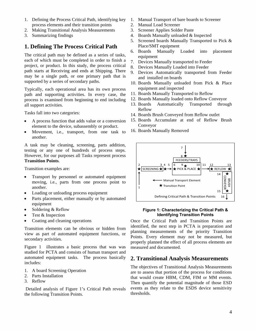
Figure 1 illustrates a basic process that was was studied for PCTA and consists of human transport and automated equipment tasks. The process basically includes:
1. A board Screening Operation 2. Parts Installation 3. Reflow
Detailed analysis of Figure 1’s Critical Path reveals the following Transition Points.
1. Manual Transport of bare boards to Screener 2. Manual Load Screener 3. Screener Applies Solder Paste 4. Boards Manually unloaded & Inspected 5. Screened boards Manually Transported to Pick &
Place/SMT equipment 6. Boards Manually Loaded into placement
equipment 7. Devices Manually transported to Feeder 8. Devices Manually Loaded into Feeder 9. Devices Automatically transported from Feeder
and installed on boards 10. Boards Manually unloaded from Pick & Place
equipment and inspected 11. Boards Manually Transported to Reflow 12. Boards Manually loaded onto Reflow Conveyor 13. Boards Automatically Transported through
Reflow 14. Boards Brush Conveyed from Reflow outlet 15. Boards Accumulate at end of Reflow Brush
Conveyor 16. Boards Manually Removed
Once the Critical Path and Transition Points are identified, the next step in PCTA is preparation and planning measurements of the priority Transition Points. Every element may not be measured, but properly planned the effect of all process elements are measured and documented.
2. Transitional Analysis Measurements The objectives of Transitional Analysis Measurements are to assess that portion of the process for conditions that would create HBM, CDM, FIM or MM events. Then quantify the potential magnitude of those ESD events as they relate to the ESDS device sensitivity thresholds.
Figure 1: Characterizing the Critical Path & Identifying Transition Points
FEEDERS/TRAYS
SCREENING PICK & PLACE REFLOW
Manual Transport Element
Transition Point
Defining Critical Path & Transition Points
BRUSH
CONVEYO
R1
2 3 4 5 6
7
8
9 10 11 12 13
14
15
16
5
The measurement may not reveal that an ESD event is taking place at that Transition Point. Rather, it may show that an assembly is being charged at that specific point in the process, only to discharge at some later time. It would also indicate how the assembly is being charged. Proper analysis will provide the probable type of ESD event the assembly will see when and if discharge occurs.
To this end, measurements include:
1. The electrostatic voltage or charge condition of ESDS devices or subassemblies: a. Prior to a transitional element b. After the transitional element c. In some cases during transitional element
2. The electrostatic voltage or charge conditions and resistance to ground of equipment, personnel, operational surfaces and materials a. Making direct contact with ESDS devices and
assemblies, or b. Producing electrostatic fields near or in the
process flow, and at transition points 3. Identifing the charged device or object’s discharge
waveform
In this study several types of measurements were made of the manufacturing process environment, grounding, equipment, personnel and materials. In all cases the authors applied traditional ESD control measurements when “auditing” the process environment. However, traditional measurements, while important, are not the subject of this study.
1. The important elements of this study are combining traditional measurement techniques with new approaches to analyzing the process and its transition points, including Body voltage measurements of personnel: a. To determine probability of exceeding process
ESD control point and incurring HBM events4 b. While transporting and handling ESDS
devices to assess the contribution of human charging to later ESD events
2. High impedance contact voltage measurements of:
a. Conductive product components, e.g., chassis or functional mechanical components, to assess potential MM events
b. ESDS devices, subassemblies and their connectors to determine potential CDM events
c. Process equipment conductive elements making direct contact with the pins/leads of devices and subassemblies, e.g., placement
heads and test probes, to assess potential MM events
d. Material handling devices and aids, e.g., device trays, totes, tape and reel, etc, for potential charge transfer to ESDS devices.
3. Field measurements in the critical path and inside automated equipement for FIM assessment
4. Continuity and resistance to ground measurements of critical process elements and surfaces, including automated equipment to confirm the element’s ability to dissipate charge to ground
5. Characterizing the probable type of ESD event that may occur by oscilloscope and CT-1 current probe examinations
III. Performing Process Capability & Transitional Analysis The Figure 1 process case study illustration consists of • Five personnel transport and handling transition
points • Screening solder paste onto circuit boards • Loading the Feeder • Placing parts on circuit boards in the Pick & Place
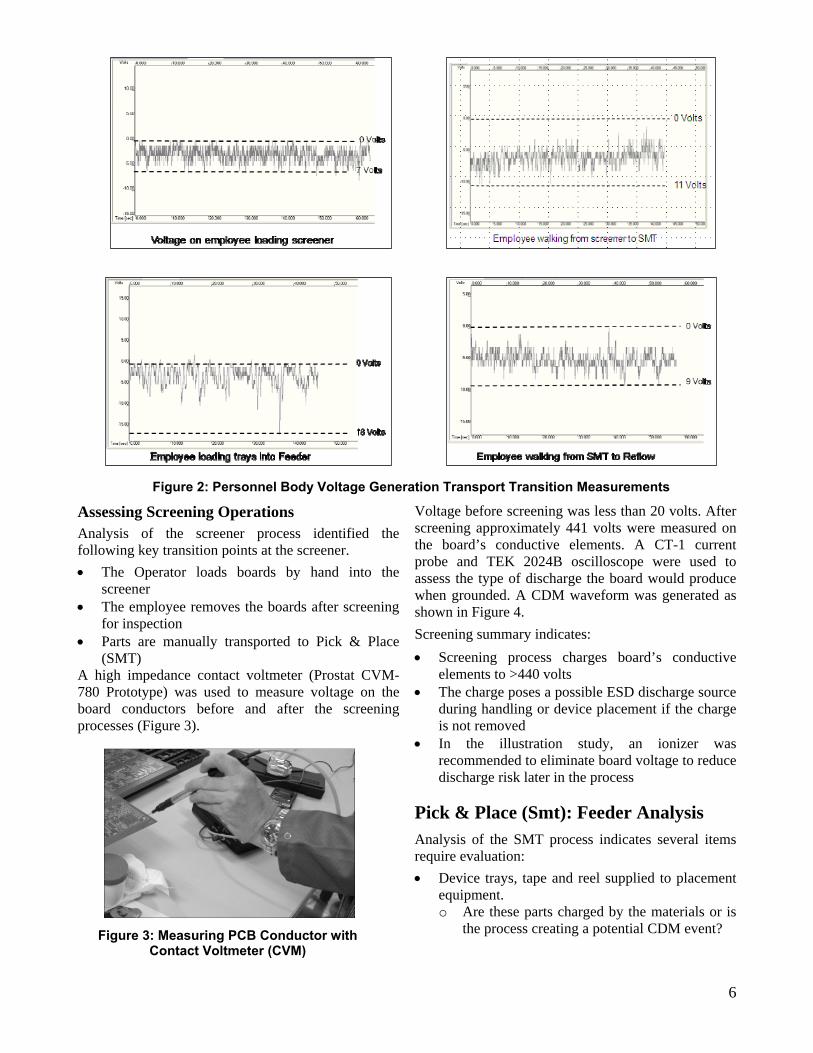
equipment • Reflow The case study Process Assessment & Transition Analysis measurements are summarized and described below. Personnel in this process wore protective footwear on an ESD controlled acrylic polished floor. Body voltage measurements of each manual transport transition were made using the following equipment:
• Charge Plate Monitor (Prostat® Corporation portable fieldmeter/charge plate [CPM] system PRF-711A & CPM-720)
• Analog to Digital (A/D) Converter & Appropriate Software (Prostat PGA-710 AutoAnalysis System® with related recording and analysis software)
• Portable Computer (IBM Notebook Computers [T-41, T-42 and X61], with Windows XP operating systems)
The results indicated very little body voltage generation in the process, or charge transfer from personnel to devices. Charts in Figure 2 documented personnel measurements at 18 volts or less.
6
Assessing Screening Operations Analysis of the screener process identified the following key transition points at the screener. • The Operator loads boards by hand into the
screener • The employee removes the boards after screening
for inspection • Parts are manually transported to Pick & Place
(SMT) A high impedance contact voltmeter (Prostat CVM-780 Prototype) was used to measure voltage on the board conductors before and after the screening processes (Figure 3).
Voltage before screening was less than 20 volts. After screening approximately 441 volts were measured on the board’s conductive elements. A CT-1 current probe and TEK 2024B oscilloscope were used to assess the type of discharge the board would produce when grounded. A CDM waveform was generated as shown in Figure 4. Screening summary indicates: • Screening process charges board’s conductive
elements to >440 volts • The charge poses a possible ESD discharge source
during handling or device placement if the charge is not removed
• In the illustration study, an ionizer was recommended to eliminate board voltage to reduce discharge risk later in the process
Pick & Place (Smt): Feeder Analysis Analysis of the SMT process indicates several items require evaluation: • Device trays, tape and reel supplied to placement
equipment. o Are these parts charged by the materials or is
the process creating a potential CDM event? Figure 3: Measuring PCB Conductor with Contact Voltmeter (CVM)
Figure 2: Personnel Body Voltage Generation Transport Transition Measurements
7
• Does the placement equipment charge the parts prior to placement on the board?
• Are there insulators in the process that may cause FIM during placement?
Consequently, this portion of the process must be broken into two parts: Analysis of the Feeder transition points and analysis of the placement equipment
The Feeder is loaded with devices that are manually transported to, then mounted in the Feeder for delivery to the SMT equipment.
• Once loaded, trays and individual devices were measured with the contact voltmeter to determine existing voltage caused by transport, that may not have dissipated after mounting in the Feeder.
• If a charge existed, the type of discharge was verified with the CT-1 and oscilloscope. The CT-1 measures current, while the scope displays voltage. The CT-1 current ratio is 5 mv = 1 ma.
As Illustration a CDM discharge (Figure 5) was recorded from a device in an improperly grounded tray. The tray was charged by manual transport in another PCTA project.
Pick & Place (Smt) Analysis SMT Analysis – Pick & Place process description includes: • Screened boards placed by hand into machine. • Conveyor moves board into position • Machine picks up IC and other devices and places
them onto the board • Conveyor moves board to machine exit The Pick & Place concerns include the following potential ESD issues: • Static generators near placement (FIM) • Isolated charged placement nozzles and other
conductive objects (MM) • Parts charged from pick up process (FIM)
Note that we previously measured the Feeder process to see if parts are charged before pickup.
• Discharge from a charged device to conductive solder paste or socket (CDM)
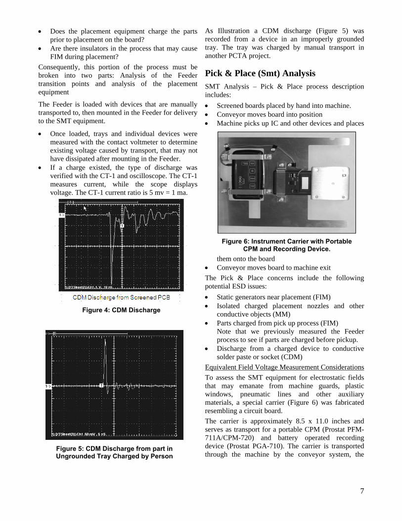
Equivalent Field Voltage Measurement Considerations To assess the SMT equipment for electrostatic fields that may emanate from machine guards, plastic windows, pneumatic lines and other auxiliary materials, a special carrier (Figure 6) was fabricated resembling a circuit board. The carrier is approximately 8.5 x 11.0 inches and serves as transport for a portable CPM (Prostat PFM-711A/CPM-720) and battery operated recording device (Prostat PGA-710). The carrier is transported through the machine by the conveyor system, the
Figure 5: CDM Discharge from part in Ungrounded Tray Charged by Person
Figure 6: Instrument Carrier with Portable CPM and Recording Device.
Figure 4: CDM Discharge

8
CPM measures the induced voltage and the recording device saves the data for later viewing (Figure 7).
The CPM plate is 15.6 pF and will see field induced voltages differently than a device. A concern is relating the measured voltages to the device sensitivity and size (capacitance) of the device. In one approach we consider the 15.6 pF plate at the midpoint of ANSI/ESD STM 5.2 CDM standard calibration references of 4 and 30 pF. However, these values do not reflect device capacitance; they are simply a reference. Another approach under consideration is to calculate equivalent device voltage based on device capacitance and CDM threshold using Q = CV. However, device capacitance varies with its proximity to ground as it moves through a process. When close to ground device capacitance is high; in free space far from ground its capacitance is very small. The following illustration assumes a device capacitance of 30 pF while in the process. • If ESDS device of 30 pF has a FIM/CDM failure
threshold of 300 volts, what is the damaging charge (Q)? o Q = CV o Q = 3.0x10 -11 F x 300 V o Q = 9.0x10⁻⁹ C, or 9.0 nC
• What Voltage measured on the 15.6 pF CPM plate is the equivalent to 9.0 nC? o V = Q/C o V = 9.0x10⁻⁹/1.56x10-11 o V = 580 Volts
Thus, if device induction threshold was 300 volts, the CPM measurement equivalent voltage limit on the 15.6 pF CPM may be 580 volts. Until device capacitance variables can be researched further, the authors document direct measurements from the 15.6 pF CPM as their PCTA reference.
Actual measurements of the internal SMT equipment fields were less than 12 volts, well below the 50 volt control point assumption. The measurement was confirmed by placing a charged material 12 inches from the machine’s critical path and transporting the
field sensing carrier past the charged material (Figure 8).
Isolated Conductors in Automated Equipment
Two symptoms of isolated conductors are: 1. Measureable voltage exists on the conductor, and 2. The conductor has no continuity to ground
In PCTA, both measurements are made to identify isolated conductors. Voltage measurements were obtained using the Contact Voltmeter (Prostat CVM-780). Resistance to ground was made with a multimeter (Fluke) and a wide range resistance system (Prostat). In the illustrated case study, all conductors in the SMT critical path were properly grounded. The device postion/placement head had less than 20 ohms resistance to ground and no measureable voltage.
CDM Measurement Options
Two options are apparent for measuring potential CDM problems in the SMT equipment. One is to program the equipment to pick up a critical device and
Figure 8: Recorded Field Voltages at 12 İnches from Charged Reference Material
Figure 9: Device Charge Sharing Measurement with Portable CPM
Figure 7: Recorded Field Voltages

9
stop the placement of the device well above board placement. Then measure the device conductors with a contact voltmeter and compare measured voltage to the ESDS device’s CDM damage threshold. This procedure was employed when assessing automated device handling equipment in other PCTA development studies.
The second procedure was used in this case study where the carrier with portable CPM and recorder was positioned at the point of device placement. Here the device is placed onto the CPM by the programed placement equipment (Figure 9). Any device voltage is shared with the CPM and stored in the recorder’s memory for later analysis (Figure 10).
CDM Equivalent Voltage Considerations The portable CPM plate is 15.6 pF and will measure device discharge voltages differently than the voltage seen by the device. This is due to the difference in device versus CPM capacitance as discussed above. Once again the discussion arises as to what the measurement can represent: • Consider the 15.6 pF plate at the midpoint of
ANSI/ESD STM 5.2 CDM standard calibration references of 4 and 30 pF, and use the measurement as a general equipment guideline. Direct measurement from the 15.6 pF plate is employed by the authors until further capacitance variables are clarified.
• Calculate the device capacitance and related discharge voltage, an analysis that is in process at this time. Once defined, one might employ Q=CV to calculate equivalent voltage.
The Feeder and SMT equipment analysis summary indicates: • IC Input properly grounded and parts are not
charged • Electrostatic fields are not a concern. < 50 volts
were measured on the CPM • Tribocharging or voltage induction of devices due
to IC handling is not a concern < 50 volts measured on the CPM at device contact
In the illustration case study the bare circuit board was charged to >440 volts at the screener. The board was not discharged and was transported by a non-charge generating person to the SMT equipment still having >350 volts on the board. At SMT output, the board voltage was >290 volts when it was transported to Reflow. The Reflow process includes: • Boards manually loaded onto metal conveyor
o Note that Boards entering Reflow in the illustration study were charged >200 volts
o The system includes a metal wire Conveyor grounded to machine frame
o Primary Concern: Are discharges occurring between charged boards and grounded metal conveyor?
• Conveyor system collects boards after reflow is completed
Board Loading (Placement) Measuring board voltage with a Contact Voltmeter prior to, and after placement onto a conductive surface will indicate: • If an ESDS assembly discharges upon contact
(CDM) • If the assembly becomes charged by the conductor
upon contact (MM)
In the illustration case study the charged board assembly discharged to the conveyor. To illustrate the discharge to host management, a Credance Aware™ RFI sensing unit equipped with local antenna was placed near the metal conveyor, and the board placement process was repeated with another circuit board measuring >200 volts. The Aware unit alarmed upon placement; board voltage was <10 volts after placement.
In other PCTA studies additional RFI measurements were effectively obtained (when used properly) using various practical techniques. In those studies, various antennae and oscilloscopes were employed and were easily implemented.
Figure 10: Device Sharing Recording in SMT

10
Reflow Accumulation Conveyor
In the illustration study the board exited Reflow with <10 volts on its conductors, then transitioned to a rotating brush conveyor (Figure 11). The board was transported to the end of the conveyor. The brush conveying system operates on an adjustable friction basis. If a board is stopped, friction increases and the brush stops turning, assuming it is properly adjusted. In the illustration study, the brushes continued to turn generating >525 volts on the boards awaiting manual transport to Cleaning and Testing.
Reflow analysis summary indicates • Discharges registered at loading of reflow
conveyor o Board charged to 200 volts o Board should be ionized prior to moving to
Reflow • Conveyor at exit of reflow charging boards to
>500 volts. o Possible discharge to grounded operators or at
next process step o Change conveyor system or add ionization
post reflow
Summarizing Process Capability & Transition Analysis Results
A basic summary of the Illustration Process Capability Analysis Study (Table 1) indicates problem areas, voltage measurements, type of potential discharge event and whether the process is within specification
Other Process Capability & Transition Analysis Examples
Several PCTA studies have been conducted in developing the concept and measurement techniques.
Important note should be made of the following observations Change in Type of Failure Model In a PCTA analysis involving high losses of RFID tags (>60% loss), the analysis identified two failure models of the same device as the critical path was measured. In one portion of the processthe RFID exhibited a CDM discharge waveform (Figure 12) . In another portion of the process the same RFID exhibited a MM discharge waveform Figure 13). Indicating that analysis of each process transition is necessary; each process segment can have a totaly different meaning to the devices in the process. Hybrid Waveforms Experimenting with transition analysis measurements in various situations, the authors recorded hybrid discharge waveforms in two areas.
1. Manual device transport 2. Garments
Figure 11: Uncontrolled Brushes Generate >500 Volts on PCBs
Figure 12: RFID Tag in Space CDM Discharge Waveform @ 100 ns
Figure 13: RFID Tag on Grounded Metal MM Discharge Waveform @ 100 ns
11
In device transport, personnel carried ESDS devices and placed them in contact with a conductor. The resulting discharge appears as combination of HBM and CDM (Figure 14).
Garment measurement and analysis have been sources of controversy for several years. The common design incorporates insulative fabrics having conductive threads woven through the material. The material is a charge generator; however, if the conductors are properly grounded electrostatic fields are suppressed. Problems arise when the garment conductors are not well grounded. Here, the electrostatic field from the surrounding insulative material couples with the conductor inducing a substantial voltage. Should the conductor(s) make contact with an ESDS device or subassembly a discharge waveform having characteristics of CDM and HBM occur.
In Figure 15, the garment discharged approximately 400 nJ of energy at 50% relative humidity.
Conclusions Process Capability and Transitional Analysis are critical requirements for determining: 1. The ability of a process to protect ESDS devices
and assemblies 2. Finding cause of ESD problems and 3. Identifying types of ESD issues in the process Measuring process is critical for ultra ESD sensitive devices because all ESD models can be found in the process Focusing on one type limits program effectiveness Can lead to ineffective changes to the process to
solve problems
References Figure 14: Device Transport Hybrid Waveform
Figure 15: Garment Discharge Hybrid Waveform
1 ESD Association, ESD/ANSI S20.20 For the Development of an Electrostatic Discharge Control Program 1 International Electrotechnical Commission (IEC), IEC 61340-5-1 Electrostatics – Part 5-1 1 ESD Association, Electrostatic Discharge (ESD) Technology Roadmap, March 4, 2005 1 M.T. Brandt and S.A. Halperin, Electrical Characterization of Floor Materials, 1990 EOS/ESD Symposium Proceedings, pp255-262

Stephen A. Halperin - President Stephen Halperin has over 30 years of industrial experience in controlling the effects of electrostatic discharge in complex applications. His background includes an undergraduate degree in Industrial Management, postgraduate work in the field of organizational communication sciences, six years of nuclear technology, and many years’ industrial manufacturing operations and management experience.Mr. Halperin formed Stephen Halperin & Associates, Limited (SH&A) in 1983, a management consulting firm specializing in electrostatic problem analysis, laboratory testing, training and static control product design. In 1992, he established Prostat Corporation for the design and manufacture of high performance electrostatic auditing instruments and ESD control materials. Mr. Halperin is known for his work in facility and process evaluation, static control techniques for highly sensitive environments, and his many contributions to the growth of the electrostatics industry and Electrostatic Discharge Association. He has lectured and consulted on static control throughout North America, Europe and the Far East, and has provided electrostatic advisory services to major corporations in several industries including Food, Drug, Chemical, Automotive, Aerospace, Electronics and Military applications.He is a charter member of the ESD Association (ESDA), has served several terms as an elected member of the ESDA Board of Directors, and over the years, chaired Local Chapter Development, Education, Professional Certification, and Standards committees. Mr. Halperin was elected to the ESDA office of Vice President in 1999, served consecutive terms as Senior Vice President and President. As a member of the Electronics Industries Association’s committee for Packaging Electronic Products for Shipment (PEPS) he served over 7 years on their Static Control Task Force #1, and participated in the development of the EIA-541 Packaging Standard. Mr. Halperin has been a long-term supporter of the Electrostatic Society of America (ESA), has been active in the ESD Symposium, and is the former Technical Advisor to ANSI’s USNC/IEC Committee. He is a recipient of the EOS/ESD Symposium’s Outstanding Paper Award, and was honored to receive the Association’s Outstanding Contribution Award for his work on behalf of industry. He is also the grateful recipient of the Joel P. Wiedendorf Memorial Award for his many ESDA Standards contributions.Mr. Halperin has delivered several papers on electrostatics and authored over 100 articles on related subjects. He is NARTE certified and a Certified ESD Program Manager Instructor. Today, he is one of the industry’s strongest supporters of ESD education and the implementation of S20.20 ESD program standards to enhance industry’s product reliability, productivity and profitability. Stephen Halperin Stephen Halperin & Associates, Ltd. 1072 Tower Lane Bensenville, IL 60106 Tel: 630-238-8883 E-mail: [email protected]

Ronald Gibson – Celestica Corporation Ron Gibson specializes in manufacturing process control, training and facility certification in accordance with ANSI/ESD S20.20. He is well known internationally as an outstanding ESD practitioner and as a major contributor to ESD technology since 1987. He is Celestica International’s Global Engineering Consultant and Corporate ESD Program Manager. He provides ESD technical guidance to all Celestica manufacturing sites, worldwide. Ron is highly experienced in manufacturing technology, packaging and all areas of ESD control in the electronic manufacturing process. As a respected member of the standards development community Ron is active in the International Electrotechnical Commission (IEC) as the Standards Council of Canada’s (SCC) national representative. In his position as Chair for IEC Technical Committee (TC) 101, Working Group 5, the important ESD Program Standard IEC 61340-5-1 and Handbook IEC 61340-5-2 were fully redeveloped to be technically equivalent to ANSI/ESD S20.20, thus harmonizing international ESD program standards. He distinguished himself by serving as the ESD Association’s Standards Chair for 10 years and publishing more industry ESD support documents than any standards chair in the history of ESDA. A member of the ESD Association since 1988, he has been active in several Standards Development Committees, a contributor to and past General Chairman of the EOS/ESD Technical Symposium, and served in every association officer’s position, including consecutive terms as Treasurer and ESDA President. As a co-founder and developer of the Professional ESD Program Manager Certification program, Ron has lectured and taught a variety of ESD courses internationally for major corporations and professional associations. Ron received the ESD industry’s highest award, the ESDA Outstanding Contribution Award, for his innovation and extensive list of technical contributions. In particular, he chaired the development and launched the ESD Association’s Facility ESD Certification program based on the ANSI/ESD S20.20 standard. This important benchmark is designed to confirm the effectiveness of a facility’s ESD control program and reduce losses, manufacturing costs, and enhance product reliability. ESD Program Certification is provided to electronics manufacturing facilities only through 3rd party ISO9000 registrars. Ron’s team has trained over 160 ISO9000 Lead Assessors globally, and to date over 200 electronics manufacturing facilities have been certified to the S20.20 Standard. During the past several years Ron has worked with SH&A on many projects. He presently supports SH&A’s ESD program design, training and facility certification preparation services through a representative agreement between SH&A and Celestica Corporation. Ronald Gibson Celestica Corporation 1150 Eglinton Avenue East Toronto, ON M3C 1H7 Tel: 416-448-5524 E-mail: [email protected]

John Kinnear Jr. – IBM Corporation John Kinnear is a specialist in process & system technology, and facility certification in accordance with ANSI/ESD S20.20. John is well known globally for his technical contributions to national and international ESD standards since 1990, and for innovations in facility certification program development. John is a Senior Engineer in the Classical Test department of IBM in Poughkeepsie, NY, where he has been the ESD Site Coordinator for the Poughkeepsie site since 1989. He is the past chairman of the IBM Inter-divisional Technical Liaison Committee for ESD Protection and is an important member of his company’s committee to develop and implement the ESD Corporate program for IBM.
A respected member of the ESD Association since 1990, John has served in several Standards Development Committees as well as association management positions. Based on his long-term contributions to ESD Standards development and in-depth technical qualifications, John is the appointed Technical Adviser to the United States National Committee/IEC Technical Committee 101, where he personally represents the United States to the International Electrotechnical Commission (IEC). In this important position he assisted in the evolution of international ESD standards and supports international adoption of ANSI/ESD S20.20.
As Vice Chair of the ESDA’s Facility Certification (ANSI/ESD S20.20) development program, John played major roles in the program’s development and industry launch. In particular, John coordinated the initial development of Lead Assessor training, ISO Registrar Certification and witness audits. Through his efforts ESD Program Certification is provided to electronics manufacturing facilities through these 3rd party ISO9000 registrars. John has trained approximately half of the global ESDA Certified ISO9000 Lead Assessors. John has made many contributions to the growth of the ESD Association. He has served in every ESD Association officer’s position, including Vice President, Senior Vice President and President. He is the past Chairman of the EOS/ESD Symposium Technical Program Committee and is presently General Chairman of the 2004 EOS/ESD Symposium.
John graduated in 1979 from the State University of Buffalo where he received a Bachelor of Science Degree in Electrical Engineering. He received his Masters of Science Degree in Electrical and Computer Engineering from Syracuse University in 1986.
During the past several years John has worked with SH&A in advisory services and product design projects. He presently supports SH&A’s ESD program design and facility certification preparation services through a representative agreement between SH&A and IBM Corporation.
John Kinnear Jr. IBM Corporation MS/P355, 2455 South Road Poughkeepsie, NY 12601 Tel: (845) 433-1473 E-mail: [email protected]

SH&A CERTIFIED ESD SPECIALISTSM PROGRAM
The SH&A Certified ESD SpecialistSM Programs prepare industry to meet the handling challenges of ultra ESD sensitive electronic devices that will be commercialized over the next 3 years. SH&A’s highly effective training curriculum provide the skills and information necessary to meet these challenges today.
LEVEL 1: PLANT AUDITOR (3 FULL DAYS)
Learning Objectives The Level 1 Plant Auditor Course will teach the fundamentals of ESD and train technicians to make the ESD Control Measurements required by ANSI/ESD S20.20 and IEC 61340-5-1 ESD Program standards including:
Worksurfaces Floors Chairs Mobile Equipment Garments Personnel Grounding (footwear, wrist straps etc…) Ionizers Gloves Hand Tools ESD Ground Verification Packaging
This course is 3 days of intensive study that includes the following subjects:
Classroom Instruction o ESD Basics for Auditors o Device Failure Models and Mechanisms o Equipment selection and use o Detailed measurement practices
Measurement Workshop
o Individual instructions on resistance and voltage measurement techniques
o Hands on practice using state-of-the-art auditing equipment
Optional Certification Exam o Candidate demonstrates proficiency in
using equipment for required audit measurements
o Successful candidates are designated as SH&A Certified ESD SpecialistSM Level 1: Plant Auditor
DATE & COST When: October 21 – 23, 2008, 8:30 a.m. - 5:00 p.m. Where: Bensenville Training Facility, Illinois Cost: $1,995. USD 5 or more: $1,595. USD
Bensenville, IL USA Chicago looks great from every angle, whether you’re exploring the city’s astonishing architecture during a guided tour or you’re enjoying the birds-eye view from the 103rd floor Sears Tower. Our Bensenville facility is only 15 min. from O’Hare Airport and 25 to 30 min. from Downtown Chicago. Doubletree® Hotel – Wood Dale / Itasca 1200 North Mittel Blvd., Wood Dale, IL USA 60191 Tel: (630) 860-2900 Fax: (630) 860-2945 Web access: http://www.doubletree.com Courtyard® by Marriott® Hotel – Wood Dale 900 N. Wood Dale Road., Wood Dale, IL USA 60191 Tel: (630) 766-7775 Fax: (630) 766-7552 Web access: http://www.marriott.com
3 exciting days of practical ESD education! “ ” © 2008 STEPHEN HALPERIN & ASSOCIATES, LTD. All rights reserved. All Seminar Materials are property of SH&A, and are protected by U.S. copyright laws.Reproduction in whole or in part without written permission is prohibited. The SH&A Logos, SH&A Certified ESD Specialist, SH&A Certified ESD Specialist, Level 1: PlantAuditor, and SH&A Certified ESD Specialist, Level 2: Designer & Administrator are Pending Service Marks of STEPHEN HALPERIN & ASSOCIATES, LTD.

Stephen Halperin & Associates, Ltd. 1072 Tower Lane
Bensenville, Illinois 60106 USA www.halperinassoc.com
Copyright 2008, All rights reserved.