product datasheet aat1185 switchregtm high voltage step-down
TRANSCRIPT
AAT1185High Voltage Step-Down ControllerSwitchRegTM
PRODUCT DATASHEET
1185.2008.12.1.1 1w w w . a n a l o g i c t e c h . c o m
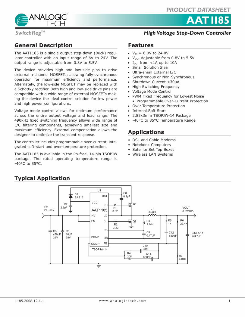
General DescriptionThe AAT1185 is a single output step-down (Buck) regu-lator controller with an input range of 6V to 24V. The output range is adjustable from 0.8V to 5.5V.
The device provides high and low-side pins to drive external n-channel MOSFETs; allowing fully synchronous operation for maximum efficiency and performance. Alternately, the low-side MOSFET may be replaced with a Schottky rectifier. Both high and low-side drive pins are compatible with a wide range of external MOSFETs mak-ing the device the ideal control solution for low power and high power configurations.
Voltage mode control allows for optimum performance across the entire output voltage and load range. The 490kHz fixed switching frequency allows wide range of L/C filtering components, achieving smallest size and maximum efficiency. External compensation allows the designer to optimize the transient response.
The controller includes programmable over-current, inte-grated soft-start and over-temperature protection.
The AAT1185 is available in the Pb-free, 14-pin TSOPJW package. The rated operating temperature range is -40°C to 85°C.
Features• VIN = 6.0V to 24.0V• VOUT Adjustable from 0.8V to 5.5V• IOUT from <1A up to 10A• Small Solution Size• Ultra-small External L/C• Synchronous or Non-Synchronous• Shutdown Current <30μA• High Switching Frequency• Voltage Mode Control• PWM Fixed Frequency for Lowest Noise▪ Programmable Over-Current Protection
• Over-Temperature Protection• Internal Soft Start• 2.85x3mm TSOPJW-14 Package• -40°C to 85°C Temperature Range
Applications• DSL and Cable Modems• Notebook Computers• Satellite Set Top Boxes• Wireless LAN Systems
Typical Application
C1033pF
R420K
VIN6V - 24V
VOUT3.3V/10A
C80.1μF
C13, C142×47μF
L13.9μH
C12680pF
C72.2μF
BST
RS
EN
HV
VCCDH
COMP
LX
DL
PGND OS
FB
AAT1185
TSOPJW-14
U1
Q1
Q2
D1BAS16
R76.04k
R627.4K
R51K
R31.74K
C90.47μF
C3470μF25V
C510μF25V
C11680pF
R13.32
R23.32
AAT1185High Voltage Step-Down ControllerSwitchRegTM
PRODUCT DATASHEET
2 1185.2008.12.1.1w w w . a n a l o g i c t e c h . c o m
AAT1185High Voltage Step-Down ControllerSwitchRegTM
PRODUCT DATASHEET
2 1185.2008.09.1.0w w w . a n a l o g i c t e c h . c o m
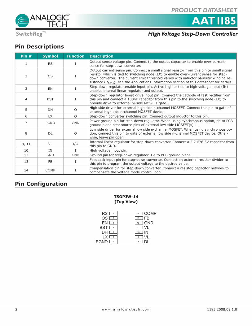
Pin Descriptions
Pin # Symbol Function Description
1 RS I Output sense voltage pin. Connect to the output capacitor to enable over-current sense for step-down converter.
2 OS I
Output current sense pin. Connect a small signal resistor from this pin to small signal resistor which is tied to switching node (LX) to enable over-current sense for step-down converter. The current limit threshold varies with inductor parasitic winding re-sistance (RDC(L)); see the Applications Information section of this datasheet for details.
3 EN I Step-down regulator enable input pin. Active high or tied to high voltage input (IN) enables internal linear regulator and output.
4 BST IStep-down regulator boost drive input pin. Connect the cathode of fast rectifi er from this pin and connect a 100nF capacitor from this pin to the switching node (LX) to provide drive to external hi-side MOSFET gate.
5 DH O High side driver for external high side n-channel MOSFET. Connect this pin to gate of external high side n-channel MOSFET device.
6 LX O Step-down converter switching pin. Connect output inductor to this pin.
7 PGND GND Power ground pin for step-down regulator. When using synchronous option, tie to PCB ground plane near source pins of external low-side MOSFET(s).
8 DL OLow side driver for external low side n-channel MOSFET. When using synchronous op-tion, connect this pin to gate of external low side n-channel MOSFET device. Other-wise, leave pin open.
9, 11 VL I/O Internal linear regulator for step-down converter. Connect a 2.2μF/6.3V capacitor from this pin to GND.
10 IN I High voltage input pin.12 GND GND Ground pin for step-down regulator. Tie to PCB ground plane.
13 FB I Feedback input pin for step-down converter. Connect an external resistor divider to this pin to program the output voltage to the desired value.
14 COMP I Compensation pin for step-down converter. Connect a resistor, capacitor network to compensate the voltage mode control loop.
Pin Configuration
TSOPJW-14(Top View)
1
2
3
4
5
6
14
13
12
11
10
9
RSOSEN
BSTDHLX
COMPFBGNDVLINVL
7 8PGND DL

AAT1185High Voltage Step-Down ControllerSwitchRegTM
PRODUCT DATASHEET
1185.2008.12.1.1 3w w w . a n a l o g i c t e c h . c o m
AAT1185High Voltage Step-Down ControllerSwitchRegTM
PRODUCT DATASHEET
1185.2008.09.1.0 3w w w . a n a l o g i c t e c h . c o m
Absolute Maximum Ratings1
TA = 25OC unless otherwise noted.
Symbol Description Value UnitsVIN(HI), VEN IN, LX, EN to GND -0.3 to 30.0 V
VIN(LO) VL to GND -0.3 to 6.0 VVBST-LX BST to LX -0.3 to 6.0 V
VCONTROL DH, DL, FB, COMP, RS, OS to PGND, GND -0.3 to VIN(LO) + 0.3 VTJ Operating Junction Temperature Range -40 to 150 °C
TLEAD Maximum Soldering Temperature (at leads, 10 sec) 300 °C
Thermal Information2
Symbol Description Value UnitsΘJA Thermal Resistance3 140 OC/WPD Maximum Power Dissipation 0.7 W
1. Stresses above those listed in Absolute Maximum Ratings may cause permanent damage to the device. Functional operation at conditions other than the operating conditions specified is not implied. Only one Absolute Maximum Rating should be applied at any one time.
2. Mounted on an FR4 board.3. Derate 7mW/°C above 25°C.
AAT1185High Voltage Step-Down ControllerSwitchRegTM
PRODUCT DATASHEET
4 1185.2008.12.1.1w w w . a n a l o g i c t e c h . c o m
AAT1185High Voltage Step-Down ControllerSwitchRegTM
PRODUCT DATASHEET
4 1185.2008.09.1.0w w w . a n a l o g i c t e c h . c o m
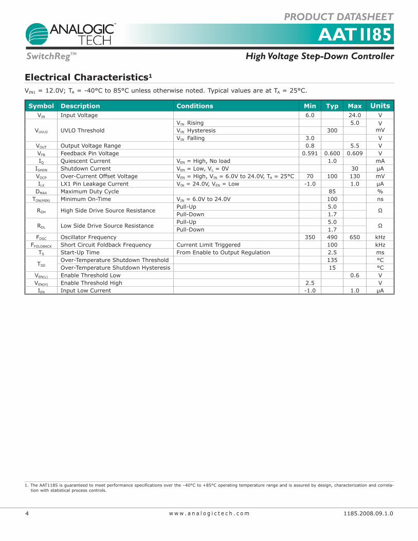
Electrical Characteristics1
VIN1 = 12.0V; TA = -40°C to 85°C unless otherwise noted. Typical values are at TA = 25°C.
Symbol Description Conditions Min Typ Max UnitsVIN Input Voltage 6.0 24.0 V
VUVLO UVLO ThresholdVIN Rising 5.0 V
mVVIN Hysteresis 300VIN Falling 3.0 V
VOUT Output Voltage Range 0.8 5.5 VVFB Feedback Pin Voltage 0.591 0.600 0.609 VIQ Quiescent Current VEN = High, No load 1.0 mA
ISHDN Shutdown Current VEN = Low, VL = 0V 30 μAVOCP Over-Current Offset Voltage VEN = High, VIN = 6.0V to 24.0V, TA = 25°C 70 100 130 mVILX LX1 Pin Leakage Current VIN = 24.0V, VEN = Low -1.0 1.0 μA
DMAX Maximum Duty Cycle 85 %TON(MIN) Minimum On-Time VIN = 6.0V to 24.0V 100 ns
RDH High Side Drive Source ResistancePull-Up 5.0
ΩPull-Down 1.7
RDL Low Side Drive Source ResistancePull-Up 5.0
ΩPull-Down 1.7
FOSC Oscillator Frequency 350 490 650 kHzFFOLDBACK Short Circuit Foldback Frequency Current Limit Triggered 100 kHz
TS Start-Up Time From Enable to Output Regulation 2.5 ms
TSDOver-Temperature Shutdown Threshold 135 °COver-Temperature Shutdown Hysteresis 15 °C
VEN(L) Enable Threshold Low 0.6 VVEN(H) Enable Threshold High 2.5 VIEN Input Low Current -1.0 1.0 μA
1. The AAT1185 is guaranteed to meet performance specifications over the –40°C to +85°C operating temperature range and is assured by design, characterization and correla-tion with statistical process controls.
AAT1185High Voltage Step-Down ControllerSwitchRegTM
PRODUCT DATASHEET
1185.2008.12.1.1 5w w w . a n a l o g i c t e c h . c o m
AAT1185High Voltage Step-Down ControllerSwitchRegTM
PRODUCT DATASHEET
1185.2008.09.1.0 5w w w . a n a l o g i c t e c h . c o m
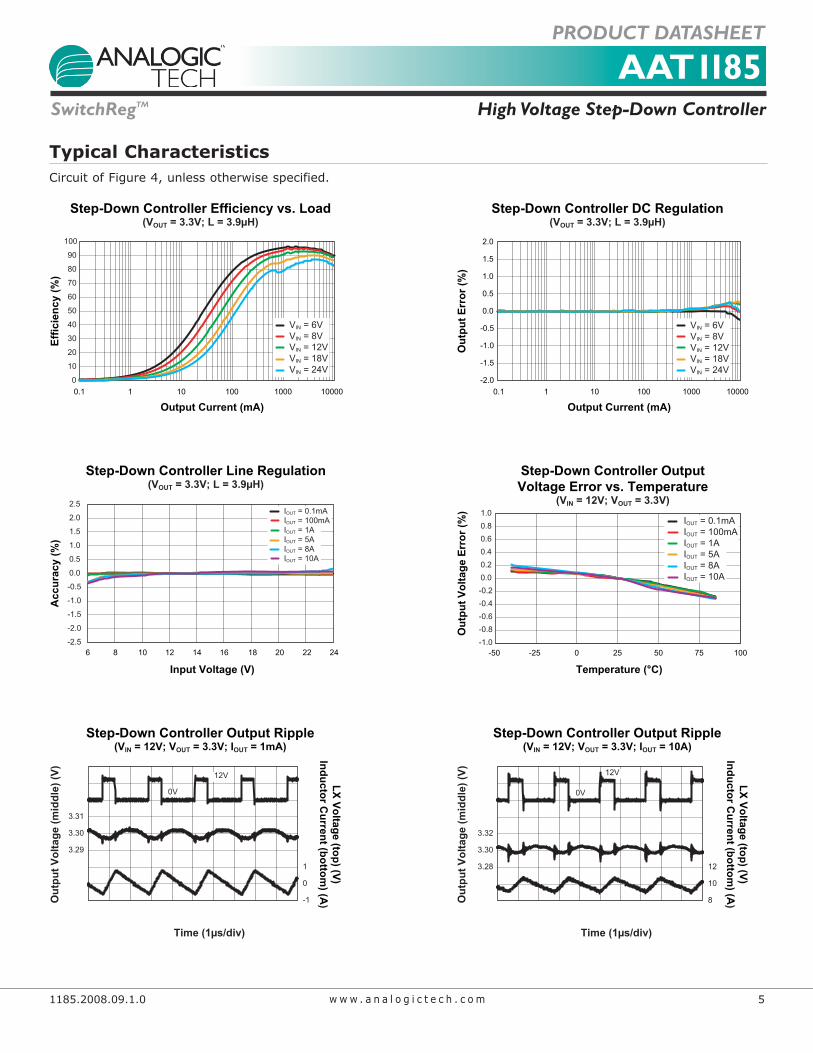
Typical CharacteristicsCircuit of Figure 4, unless otherwise specified.
Step-Down Controller Efficiency vs. Load(VOUT = 3.3V; L = 3.9µH)
Output Current (mA)
Effic
ienc
y (%
)
0.1 1 10 100 1000 100000
10
20
30
40
50
60
70
80
90
100
VIN = 6VVIN = 8V VIN = 12VVIN = 18VVIN = 24V
Step-Down Controller DC Regulation(VOUT = 3.3V; L = 3.9µH)
Output Current (mA)
Out
put E
rror
(%)
-2.0
-1.5
-1.0
-0.5
0.0
0.5
1.0
1.5
2.0
0.1 1 10 100 1000 10000
VIN = 6VVIN = 8V VIN = 12VVIN = 18VVIN = 24V
Step-Down Controller Line Regulation(VOUT = 3.3V; L = 3.9µH)
Input Voltage (V)
Acc
urac
y (%
)
6 8 10 12 14 16 18 20 22 24-2.5
-2.0
-1.5
-1.0
-0.5
0.0
0.5
1.0
1.5
2.0
2.5IOUT = 0.1mAIOUT = 100mAIOUT = 1AIOUT = 5AIOUT = 8AIOUT = 10A
Step-Down Controller OutputVoltage Error vs. Temperature
(VIN = 12V; VOUT = 3.3V)
Temperature (°C)
Out
put V
olta
ge E
rror
(%)
-50 -25 0 25 75 10050-1.0-0.8-0.6-0.4-0.20.00.20.40.60.81.0
IOUT = 0.1mAIOUT = 100mAIOUT = 1AIOUT = 5AIOUT = 8AIOUT = 10A
Step-Down Controller Output Ripple(VIN = 12V; VOUT = 3.3V; IOUT = 1mA)
Time (1µs/div)
Out
put V
olta
ge (m
iddl
e) (V
)
LX Voltage (top) (V)Inductor C
urrent (bottom) (A
)
3.29
3.30
3.31
-1
0
1
0V
12V
Step-Down Controller Output Ripple(VIN = 12V; VOUT = 3.3V; IOUT = 10A)
Time (1µs/div)
Out
put V
olta
ge (m
iddl
e) (V
)
LX Voltage (top) (V)Inductor C
urrent (bottom) (A
)
3.28
3.30
3.32
8
10
12
0V
12V
AAT1185High Voltage Step-Down ControllerSwitchRegTM
PRODUCT DATASHEET
6 1185.2008.12.1.1w w w . a n a l o g i c t e c h . c o m
AAT1185High Voltage Step-Down ControllerSwitchRegTM
PRODUCT DATASHEET
6 1185.2008.09.1.0w w w . a n a l o g i c t e c h . c o m
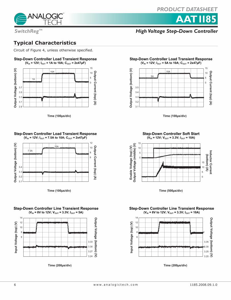
Typical CharacteristicsCircuit of Figure 4, unless otherwise specified.
Step-Down Controller Load Transient Response(VIN = 12V; IOUT = 1A to 10A; COUT = 2x47µF)
Time (100µs/div)
Out
put V
olta
ge (b
otto
m) (
V) Output C
urrent (top) (A)
2.9
3.1
3.3
3.5
3.7
0
5
10
15
1A
10A
Step-Down Controller Load Transient Response(VIN = 12V; IOUT = 5A to 10A; COUT = 2x47µF)
Time (100µs/div)
Out
put V
olta
ge (b
otto
m) (
V) Output C
urrent (top) (A)
3.1
3.2
3.3
3.4
3.5
0
5
10
15
5A
10A
Step-Down Controller Load Transient Response(VIN = 12V; IOUT = 7.5A to 10A; COUT = 2x47µF)
Time (100µs/div)
Out
put V
olta
ge (b
otto
m) (
V) Output C
urrent (top) (A)
3.1
3.2
3.3
3.4
6
8
10
12
7.5A
10A
Step-Down Controller Soft Start(VIN = 12V; VOUT = 3.3V; IOUT = 10A)
Time (500µs/div)
Enab
le V
olta
ge (t
op) (
V)O
utpu
t Vol
tage
(mid
dle)
(V)
Inductor Current
(bottom) (A
)
0
5
10
15
0
5
10
15
Step-Down Controller Line Transient Response(VIN = 8V to 12V; VOUT = 3.3V; IOUT = 5A)
Time (200µs/div)
Inpu
t Vol
tage
(top
) (V)
Output Voltage (bottom
) (V)
6
8
10
12
14
3.24
3.27
3.30
3.33
Step-Down Controller Line Transient Response(VIN = 8V to 12V; VOUT = 3.3V; IOUT = 10A)
Time (200µs/div)
Inpu
t Vol
tage
(top
) (V)
Output Voltage (bottom
) (V)
6
8
10
12
14
3.20
3.25
3.30
3.35
AAT1185High Voltage Step-Down ControllerSwitchRegTM
PRODUCT DATASHEET
1185.2008.12.1.1 7w w w . a n a l o g i c t e c h . c o m
AAT1185High Voltage Step-Down ControllerSwitchRegTM
PRODUCT DATASHEET
1185.2008.09.1.0 7w w w . a n a l o g i c t e c h . c o m
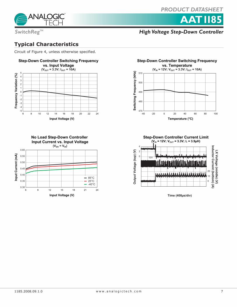
Typical CharacteristicsCircuit of Figure 4, unless otherwise specified.
Step-Down Controller Switching Frequencyvs. Input Voltage
(VOUT = 3.3V; IOUT = 10A)
Input Voltage (V)
Freq
uenc
y Va
riatio
n (%
)
6 8 10 12 14 16 18 20 22 24-5-4-3-2-1012345
Step-Down Controller Switching Frequencyvs. Temperature
(VIN = 12V; VOUT = 3.3V; IOUT = 10A)
Temperature (°C)
Switc
hing
Fre
quen
cy (k
Hz)
-40 -20 0 20 40 60 80 100470
480
490
500
510
No Load Step-Down Controller Input Current vs. Input Voltage
(VEN = VIN)
Input Voltage (V)
Inpu
t Cur
rent
(mA
)
6 9 12 15 18 21 240.30
0.35
0.40
0.45
0.50
0.55
0.60
85°C25°C -40°C
Step-Down Controller Current Limit(VIN = 12V; VOUT = 3.3V; L = 3.9µH)
Time (400µs/div)
Out
put V
olta
ge (t
op) (
V)
LX Voltage (middle) (V)
Inductor Current (bottom
) (A)
0
2
4
0
10
20
12V

AAT1185High Voltage Step-Down ControllerSwitchRegTM
PRODUCT DATASHEET
8 1185.2008.12.1.1w w w . a n a l o g i c t e c h . c o m
AAT1185High Voltage Step-Down ControllerSwitchRegTM
PRODUCT DATASHEET
8 1185.2008.09.1.0w w w . a n a l o g i c t e c h . c o m
Applications InformationThe AAT1185 is a single output step-down (Buck) regu-lator controller with an input range of 6V to 24V. The output range is adjustable from 0.8V to 5.5V.
The device provides high and low-side pins to drive external n-channel MOSFETs; allowing fully synchronous operation for maximum efficiency and performance. Alternatively, the low-side MOSFET may be replaced with a Schottky rectifier and the DL pin left open. Both high and low-side drive pins are compatible with a wide range of external MOSFETs making the device the ideal control solution for low power and high power configurations.
Voltage mode control allows for optimum performance across the entire output voltage and load range. 490kHz fixed switching frequency allows wide range of L/C filter-ing components, achieving smallest size and maximum efficiency. External compensation allows the designer to optimize the transient response components.
The controller includes programmable over-current, inte-grated soft-start and over-temperature protection.
The AAT1185 is available in the Pb-free, 14-pin TSOPJW package. The rated operating temperature range is -40°C to 85°C.
Regulator Output Capacitor Selection
Two 47μF ceramic output capacitors are required to filter the inductor current ripple and supply the load transient current for IOUT = 10A. The 1210 package with 10V minimum voltage rating is recommended for the output capacitors to maintain a minimum capacitance drop with DC bias.
Output Inductor Selection
The step-down converter utilizes constant frequency (PWM-mode) voltage mode control. A 3.9μH to 4.7μH inductor value with appropriate DCR is selected to main-tain the desired output current ripple and minimize the
Functional Block Diagram
Logic
ErrorAmp
Control LogicEN
OT
VoltageRef
VLVINT
Comp.
Reg.
LX
BST
IN
RSOS
Logic
ErrorAmp
Control Logic
EN
FB
OSCOT
VoltageRef
Comp.
Reg.
DH
PGND
DL
COMP
Comp
VOCP
= 0.1V
AAT1185High Voltage Step-Down ControllerSwitchRegTM
PRODUCT DATASHEET
1185.2008.12.1.1 9w w w . a n a l o g i c t e c h . c o m
converter’s response time to load transients. The peak switch current should not exceed the inductor saturation current of the MOSFETs. The DCR of the inductor sets the designed current limit in the following formula:
ILIM = 100mVDCR
For 10A output load, the selected DCR should be less than 10mΩ to avoid the peak inductor current triggers the current limit.
MOSFET Selection
The step-down (buck) converter utilizes synchronous rectification (Q1) for constant frequency (PWM mode) voltage mode control. The synchronous rectifier is selected based on the desired RDS(ON) value and QG (total gate charge), these two critical parameters are weighed against each other. To get a low RDS(ON) value, the MOSFET must be very large; a larger MOSFET will have a large QG. Conversely, to get a low QG, the MOSFET must be small and thus have a large RDS(ON) value. In addition to the trade off between RDS(ON) and QG, the maximum voltage rating for the external synchronous MOSFET must exceed the maximum application input voltage value (VDS [max] > VIN [max]).
The QG affects the turn-on/turn-off time of the synchro-nous MOSFET; the longer the turn-on/turn-off time, the more likely the step-down converter will have “shoot-through” current issues. “Shoot-through” current occurs when the high-side MOSFET and the low-side MOSFET are conducting current at the same time. This will result in a low impedance path to ground from the input volt-age through the two MOSFETs, and the current may exceed the maximum current rating of the MOSFETs. Exceeding the maximum current ratings will lead to the destructive derating of the MOSFETs.
The critical parameter recommendations for the external minimum 25V MOSFET are as follows:
QG (Total Gate Charge): 5nC to 15nC (max)(VGS: 4.5V to 5V)RDS(ON): 10mΩ to 30mΩ (max) (VGS: 4.5V to 5V)
Input Capacitor Selection
For low-cost applications, a 470μF/25V electrolytic capacitor is selected to control the voltage overshoot across the high side MOSFET. A 10μF/25V ceramic capacitor with a voltage rating at least 1.05 times great-er than the maximum input voltage is connected as close
as possible to the input pins (Pins 9 and 11) for high frequency decoupling.
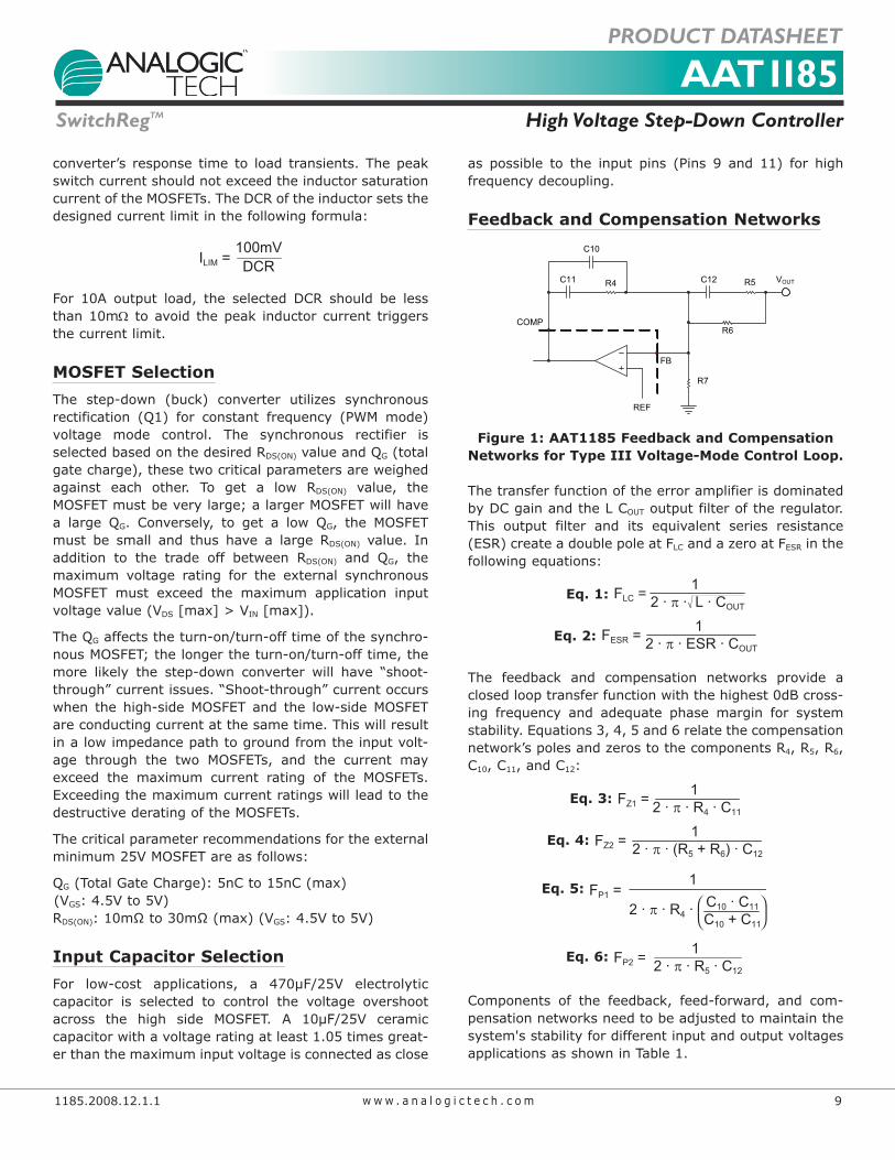
Feedback and Compensation Networks
R7
R6
R4 R5C12C11
C10
FB
VOUT
COMP
REF
Figure 1: AAT1185 Feedback and Compensation Networks for Type III Voltage-Mode Control Loop.
The transfer function of the error amplifier is dominated by DC gain and the L COUT output filter of the regulator. This output filter and its equivalent series resistance (ESR) create a double pole at FLC and a zero at FESR in the following equations:
Eq. 1: FLC = 1
2 · π · L · COUT
Eq. 2: FESR = 1
2 · π · ESR · COUT
The feedback and compensation networks provide a closed loop transfer function with the highest 0dB cross-ing frequency and adequate phase margin for system stability. Equations 3, 4, 5 and 6 relate the compensation network’s poles and zeros to the components R4, R5, R6, C10, C11, and C12:
Eq. 3: FZ1 = 1
2 · π · R4 · C11
Eq. 4: FZ2 = 1
2 · π · (R5 + R6) · C12
Eq. 5: 1
FP1 =
2 · π · R4 · C10 · C11
C10 + C11
Eq. 6: FP2 = 1
2 · π · R5 · C12
Components of the feedback, feed-forward, and com-pensation networks need to be adjusted to maintain the system's stability for different input and output voltages applications as shown in Table 1.
AAT1185High Voltage Step-Down ControllerSwitchRegTM
PRODUCT DATASHEET
10 1185.2008.12.1.1w w w . a n a l o g i c t e c h . c o m
Over-Current Protection
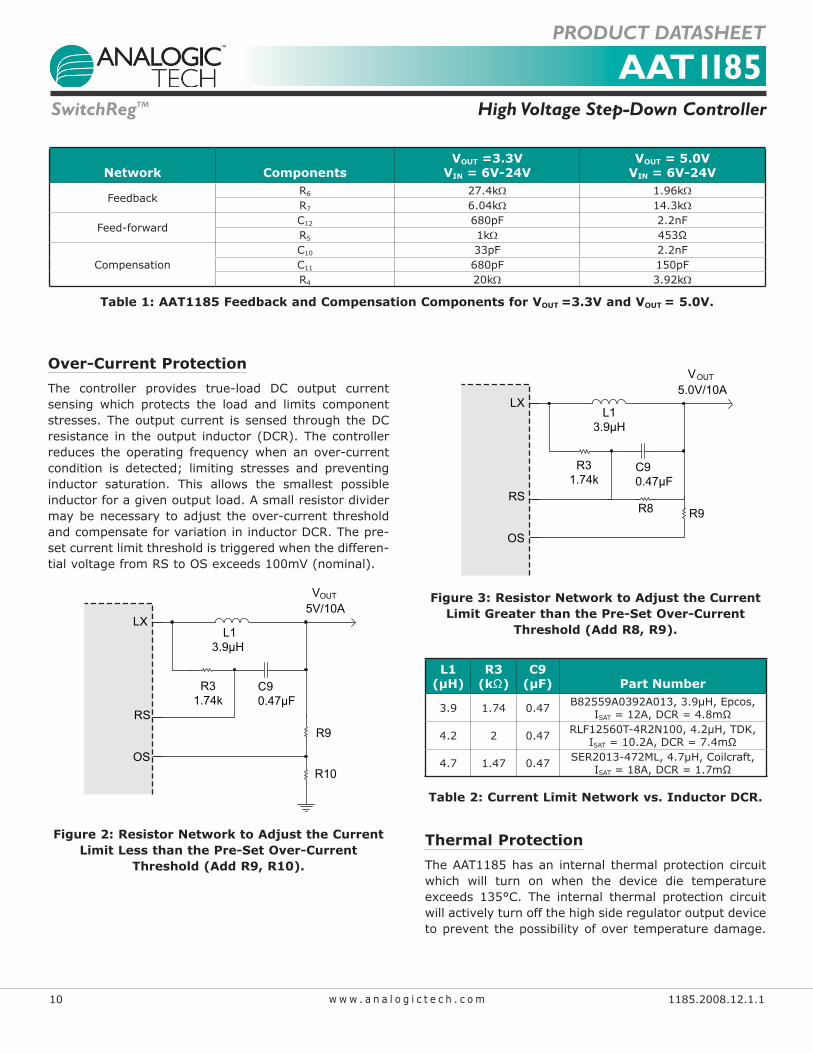
The controller provides true-load DC output current sensing which protects the load and limits component stresses. The output current is sensed through the DC resistance in the output inductor (DCR). The controller reduces the operating frequency when an over-current condition is detected; limiting stresses and preventing inductor saturation. This allows the smallest possible inductor for a given output load. A small resistor divider may be necessary to adjust the over-current threshold and compensate for variation in inductor DCR. The pre-set current limit threshold is triggered when the differen-tial voltage from RS to OS exceeds 100mV (nominal).
R31.74k
C90.47μF
5V/10A
L13.9μH
R9
R10
VOUT
OS
RS
LX
Figure 2: Resistor Network to Adjust the Current Limit Less than the Pre-Set Over-Current
Threshold (Add R9, R10).
R31.74k
C90.47μF
5.0V/10A
L13.9μH
R9R8
VOUT
OS
RS
LX
Figure 3: Resistor Network to Adjust the Current Limit Greater than the Pre-Set Over-Current
Threshold (Add R8, R9).
L1 (μH)
R3 (kΩ)
C9 (μF) Part Number
3.9 1.74 0.47 B82559A0392A013, 3.9μH, Epcos, ISAT = 12A, DCR = 4.8mΩ
4.2 2 0.47 RLF12560T-4R2N100, 4.2μH, TDK, ISAT = 10.2A, DCR = 7.4mΩ
4.7 1.47 0.47 SER2013-472ML, 4.7μH, Coilcraft, ISAT = 18A, DCR = 1.7mΩ
Table 2: Current Limit Network vs. Inductor DCR.
Thermal Protection
The AAT1185 has an internal thermal protection circuit which will turn on when the device die temperature exceeds 135°C. The internal thermal protection circuit will actively turn off the high side regulator output device to prevent the possibility of over temperature damage.
Network ComponentsVOUT =3.3V
VIN = 6V-24V VOUT = 5.0V
VIN = 6V-24V
FeedbackR6 27.4kΩ 1.96kΩR7 6.04kΩ 14.3kΩ
Feed-forwardC12 680pF 2.2nFR5 1kΩ 453Ω
CompensationC10 33pF 2.2nFC11 680pF 150pFR4 20kΩ 3.92kΩ
Table 1: AAT1185 Feedback and Compensation Components for VOUT =3.3V and VOUT = 5.0V.
AAT1185High Voltage Step-Down ControllerSwitchRegTM
PRODUCT DATASHEET
1185.2008.12.1.1 11w w w . a n a l o g i c t e c h . c o m
The Buck regulator output will remain in a shutdown state until the internal die temperature falls back below the 135°C trip point. The combination and interaction between the short circuit and thermal protection sys-tems allows the Buck regulator to withstand indefinite short-circuit conditions without sustaining permanent damage.
Thermal Calculations
There are three types of losses associated with the AAT1185 step-down converter: switching losses, con-duction losses, and quiescent current losses. Conduction losses are associated with the RDS(ON) characteristics of the power output switching devices. Switching losses are dominated by the gate charge of the power output switching devices. At full load, assuming continuous con-duction mode (CCM), a simplified form of the synchro-nous step-down converter and LDO losses is given by:
PTOTALIOUT
2 · (RDS(ON)H · VOUT + RDS(ON)L · [VIN - VOUT])
+ (tSW · FS · IOUT + IQ) · VIN
VIN=
IQ1 is the step-down converter quiescent currents. The term tSW is used to estimate the full load step-down con-verter switching losses.
The power dissipation that relates to the RDS(ON) occurs in the external high side and low side MOSFETs. Therefore, the total package losses for AAT1185 reduce to the fol-lowing equation:
PTOTAL = (tSW · FS · IOUT + IQ1) · VIN1
Since quiescent current, and switching losses all vary with input voltage, the total losses should be investi-gated over the complete input voltage range.
Given the total losses, the maximum junction tempera-ture can be derived from the θJA for the TSOPJW-14 package, which is 140°C/W.
TJ(MAX) = PTOTAL · θJA + TAMB
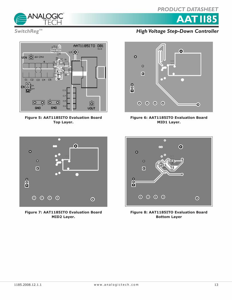
Layout Considerations
The suggested PCB layout for the AAT1185 is shown in Figures 5, 6, 7, and 8. The following guidelines should be used to help ensure a proper layout.
1. The power input capacitors (C3 and C5) should be connected as closely as possible to the high voltage input pin (IN) and power ground.
2. C5, L1, Q1, C13, and C14 should be placed as close-ly as possible to each other to minimize any para-sitic inductance in the switched current path, which generates a large voltage spike during the switching interval. The connection of inductor to switching node should be as short as possible.
3. The feedback trace or FB pin should be separated from any power trace and connected as closely as possible to the load point. Sensing along a high-current load trace will degrade DC load regulation.
4. The resistance of the trace from the load returns to PGND should be kept to a minimum. This will help to minimize any error in DC regulation due to differ-ences in the potential of the internal signal ground and the power ground.
5. Connect unused signal pins to ground to avoid unwanted noise coupling.
6. The critical small signal components, include feed-back components and compensation components, should be placed close to the FB1 and COMP1 pins. The feedback resistors should be located as close as possible to the FB1 pin with its ground tied straight to the signal ground plane, which is separated from the power ground plane.
7. C9 and R3 should be connected as closely as possi-ble to the RS1 and OS1 pins and placed on the bot-tom side of the layout to avoid noise coupling from the inductor.
8. For good thermal coupling, a 4-layer PCB layout is recommended and PCB vias are required from the exposed pad (EP) for the MOSFETs paddle to the middle plane and bottom plane.

AAT1185High Voltage Step-Down ControllerSwitchRegTM
PRODUCT DATASHEET
12 1185.2008.12.1.1w w w . a n a l o g i c t e c h . c o m
C10
R31.74K
R420K
VIN
6V - 24VVOUT
3.3V/10A
C90.47μF
0.1μFC8
C13, C142x47μF
C15, C16open
3.9μH
L1
680pFC12
C72.2μF
BST 4
RS 1GND12
EN3
HV10
VCC11
VCC9 DH 5
COMP14
LX6
DL 8
PGND7 OS 2
FB 13
AAT1185
TSOPJW-14
U1
Si7326DNQ1
Si7326DNQ2
BAS16D1
1kR5
R627.4K
R76.04k
1
2
3
EN
C3470μF25V
C510μF25V
C1, C2,C4, C6open
C11680pF
U1 AAT1185 Analogic Technologies, Hi-Voltage Buck Controller, TSOPJW-14C3 Cap, MLC, 470μF/25V, ElectrolyticC5 Cap, MLC, 10μF/25V, 1210C7 Cap, MLC, 2.2μF/6.3V, 0603C8 Cap, MLC, 0.1μF/6.3V, 0603C9 Cap, MLC, 0.47μF/6.3V, 0603C10, C11, C12 Cap, MLC, misc, 0402C13, C14 Cap, MLC, 47μF/10V, 1210R1-R7 Carbon film resistor, 0402D1 BAS16, Generic, Rectifier, 0.2A/85V, Ultrafast, SOT23Q1, Q2 Si7326DN, Vishay, N-Channel, 30V, 10A, PAK 1212-8 L1 B82559A0392A013, 3.9μH, Epcos, ISAT = 12A, DCR = 4.8mΩL1 RLF12560T-4R2N100, 4.2μH, TDK, ISAT = 10.2A, DCR = 7.4mΩL1 SER2013-472ML, 4.7μH, Coicraft, ISAT = 18A, DCR = 1.7mΩ
3.32
R1
3.32
R2
33pF
Figure 4: AAT1185ITO Evaluation Board Schematic for VIN = 6V-24V and VOUT = 3.3V.
AAT1185High Voltage Step-Down ControllerSwitchRegTM
PRODUCT DATASHEET
1185.2008.12.1.1 13w w w . a n a l o g i c t e c h . c o m
Figure 5: AAT1185ITO Evaluation Board Figure 6: AAT1185ITO Evaluation Board Top Layer. MID1 Layer.
Figure 7: AAT1185ITO Evaluation Board Figure 8: AAT1185ITO Evaluation Board MID2 Layer. Bottom Layer

AAT1185High Voltage Step-Down ControllerSwitchRegTM
PRODUCT DATASHEET
14 1185.2008.12.1.1w w w . a n a l o g i c t e c h . c o m
AAT1185 Design Example
Specifications
VO = 3.3V @ 10A, Pulsed Load ΔILOAD = 10AVIN = 12VFS = 490kHzTAMB = 85°C in TSOPJW-14 Package
Output Inductor
For Epcos inductor B82559A0392A013, 3.9μH, DCR = 4.8mΩ max.
ΔI = · 1 - = · 1 - = 1.25A
IPK1 = IOUT1 + = 10A + 0.6A = 10.6A
PL1 = IOUT12 · DCR = 10.6A2 · 4.8mΩ = 539mW
VOUT
L1 · FS
ΔI2
VOUT
VIN
3.3V12V
3.3V3.9μH · 490kHz
Output Capacitor
VDROOP = 0.6V
12 3
1 3.3V · (24V - 3.3V) 3.9μH · 490kHz · 24V 2 3RMS(MAX) = · I
L · FS · VIN(MAX)·
3 · ΔILOAD
VDROOP · FS
3 · 10A0.6V · 490kHz
COUT = = = 102μF; use 2x47μF
· = 430mARMS·
VOUT · (VIN(MAX) - VOUT) =
PRMS = ESR · IRMS2 = 5mΩ · (430mA)2 = 0.9mW
Input Capacitor
Input Ripple VPP = 60mV
CIN = = = 510μF
1
- ESR · 4 · FSVPP
IOUT
1
- 5mΩ · 4 · 490kHz60mV10A
For low cost applications, a 470μF/25V electrolytic capacitor in parallel with a 10μF/25V ceramic capacitor is used to reduce the ESR.
IOUT1
2RMSI
P = ESR · (IRMS)2 = 5mΩ · (5A)2 = 125mW
= = 5A
AAT1185High Voltage Step-Down ControllerSwitchRegTM
PRODUCT DATASHEET
1185.2008.12.1.1 15w w w . a n a l o g i c t e c h . c o m
Current Limit
Over-current offset voltage VOCP = 100mVTotal trace parasitic resistor and inductor DCR is 6mΩ
100mV ILIMIT = = = 17A6mΩ
VS DCR
In order to sense the inductor current correctly during dynamic operation the R-C network time constant R3 *C9 should match the inductor time constant L1/DCR:
= R3 · C9 L1
DCR
Choose C3 = 0.47μF
L1
DCR · C9R3 =
3.9μH4.8mΩ · 0.47μF
= = 1.74kΩ
AAT1185 Losses
All values assume 25°C ambient temperature and thermal resistance of 140°C/W in the TSOPJW-12 package.
PTOTAL = (tSW · FS · IOUT1 + IQ) · VIN
PTOTAL = (5ns · 490kHz · 10A + 70μA) · 12V
PTOTAL = 295mW
TJ(MAX) = TAMB + ΘJA · PLOSS = 85°C + (140°C/W) · 0.295mW = 126.3°C

AAT1185High Voltage Step-Down ControllerSwitchRegTM
PRODUCT DATASHEET
16 1185.2008.12.1.1w w w . a n a l o g i c t e c h . c o m
AAT1185High Voltage Step-Down ControllerSwitchRegTM
PRODUCT DATASHEET
16 1185.2008.09.1.0w w w . a n a l o g i c t e c h . c o m
Ordering Information
Package Voltage Marking1 Part Number (Tape and Reel)2
TSOPJW-14 Adj (0.6V) 4UXYY AAT1185ITO-0.6-T1
All AnalogicTech products are offered in Pb-free packaging. The term “Pb-free” means semiconductor products that are in compliance with current RoHS standards, including the requirement that lead not exceed 0.1% by weight in homogeneous materials. For more information, please visit our website at http://www.analogictech.com/about/quality.aspx.
Package Information
TSOPJW-142.
40 ±
0.1
0
2.85
± 0
.20
0.40 BSC
0.20 + 0.10 - 0.05
0.15
± 0
.05
0.04 REF
0.45 ± 0.15
2.75 ± 0.25
4° ± 4°
1.05
+ 0
.05
- 0
.00
1.00
+ 0
.000
- 0.0
75
3.05 + 0.05 - 0.10
0.05 + 0.05 - 0.04
Top View
Side View End View
All dimensions in millimeters.
1. XYY = assembly and date code. 2. Sample stock is generally held on part numbers listed in BOLD.
AAT1185High Voltage Step-Down ControllerSwitchRegTM
PRODUCT DATASHEET
1185.2008.12.1.1 17w w w . a n a l o g i c t e c h . c o m
AAT1185High Voltage Step-Down ControllerSwitchRegTM
PRODUCT DATASHEET
1185.2008.09.1.0 17w w w . a n a l o g i c t e c h . c o m
Advanced Analogic Technologies, Inc.3230 Scott Boulevard, Santa Clara, CA 95054Phone (408) 737-4600Fax (408) 737-4611
© Advanced Analogic Technologies, Inc.AnalogicTech cannot assume responsibility for use of any circuitry other than circuitry entirely embodied in an AnalogicTech product. No circuit patent licenses, copyrights, mask work rights, or other intellectual property rights are implied. AnalogicTech reserves the right to make changes to their products or specifi cations or to discontinue any product or service without notice. Except as provided in AnalogicTech’s terms and conditions of sale, AnalogicTech assumes no liability whatsoever, and AnalogicTech disclaims any express or implied warranty relating to the sale and/or use of AnalogicTech products including liability or warranties relating to fi tness for a particular purpose, merchantability, or infringement of any patent, copyright or other intellectual property right. In order to minimize risks associated with the customer’s applications, adequate design and operating safeguards must be provided by the customer to minimize inherent or procedural hazards. Testing and other quality control techniques are utilized to the extent AnalogicTech deems necessary to support this warranty. Specifi c testing of all parameters of each device is not necessarily performed. AnalogicTech and the AnalogicTech logo are trademarks of Advanced Analogic Technologies Incorporated. All other brand and product names appearing in this document are registered trademarks or trademarks of their respective holders.