product introduction: mg3700a vector signal generator · product introduction mg3700a vector signal...
TRANSCRIPT

Product Introduction
MG3700A Vector Signal Generator

Slide 1
MG3700A-E-I-1
Product Introduction
Anritsu Corporation
November 2012
(11.00)
Slide 2
MG3700A-E-I-1
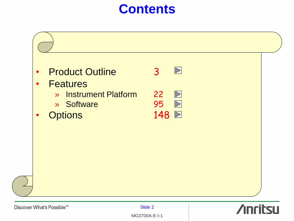
Contents
• Product Outline 3
• Features » Instrument Platform 22
» Software 95
• Options 148

Slide 3
MG3700A-E-I-1
Product Outline
• Product Outline
• Features
• Options
• Market 4
• Product Concept 7
• All-round Applications 19

Slide 4
MG3700A-E-I-1
Best Value Required
Your vector signal generator requirements have never
been tougher, and yet your capital equipment budget has
never been tighter. You need the most value you can get
in a vector signal generator. You need a vector signal
generator that meets today's needs yet can be diverted to
satisfy future requirements without shattering your test
equipment budget. The MG3700A Vector Signal
Generator delivers the best value required today at a
reasonable cost: » Adaptable to next generation markets
» Utilizable to evaluate equipment, baseband chips, and
components for broadband wireless communication

Slide 5
MG3700A-E-I-1
Market Trends
• Mobile communication systems are evolving to higher
speeds and increased wideband modulation. » Cellular phones and WLANs are evolving into new wireless
systems using more information.
• Broadcast and information service systems are
developing toward digitization. » They are changing from analog modulation to digital modulation
for advanced information services and frequency-effective
utilization.
• A wide variety of new wireless systems, such as last mile
and personal communications (WPAN), have appeared. » In order to increase cordless mobility, various new wireless
systems are being introduced.

Slide 6
MG3700A-E-I-1
Major Vector Signal Generator Applications
• Wanted signal source and interference signal source for
receiver testing » Receiver sensitivity test needs a wanted signal source. Receiver
interference response test also needs interference signal
sources.
• Reference signal source for evaluating components and
devices » For components, such as power amplifiers, filters, mixers, and
modulator/demodulators, path performance and distortion
(spectral regrowth) are measured using signal generators and
signal analyzers.
• Reference signal source for verifying baseband chips » Baseband chips are verified their decoding algorithms and
processing flows in physical layer during their development
phase.

Slide 7
MG3700A-E-I-1
Product Concept
• Wideband modulation capability adaptable up to 4G
• Includes an all-round and high-speed arbitrary waveform
(ARB) I/Q baseband generator as standard equipment
• Includes baseband memory and hard disk that store
large-volume baseband signal data as standard
equipment
• Includes BER analyzer required for receiver sensitivity
test as standard equipment
• Fast switching, high reliability, and high level accuracy for
ATE
• Ethernet remote operation to make maintenance
management easy
• Weight saving to increase mobility
• Ecological design
Slide 8
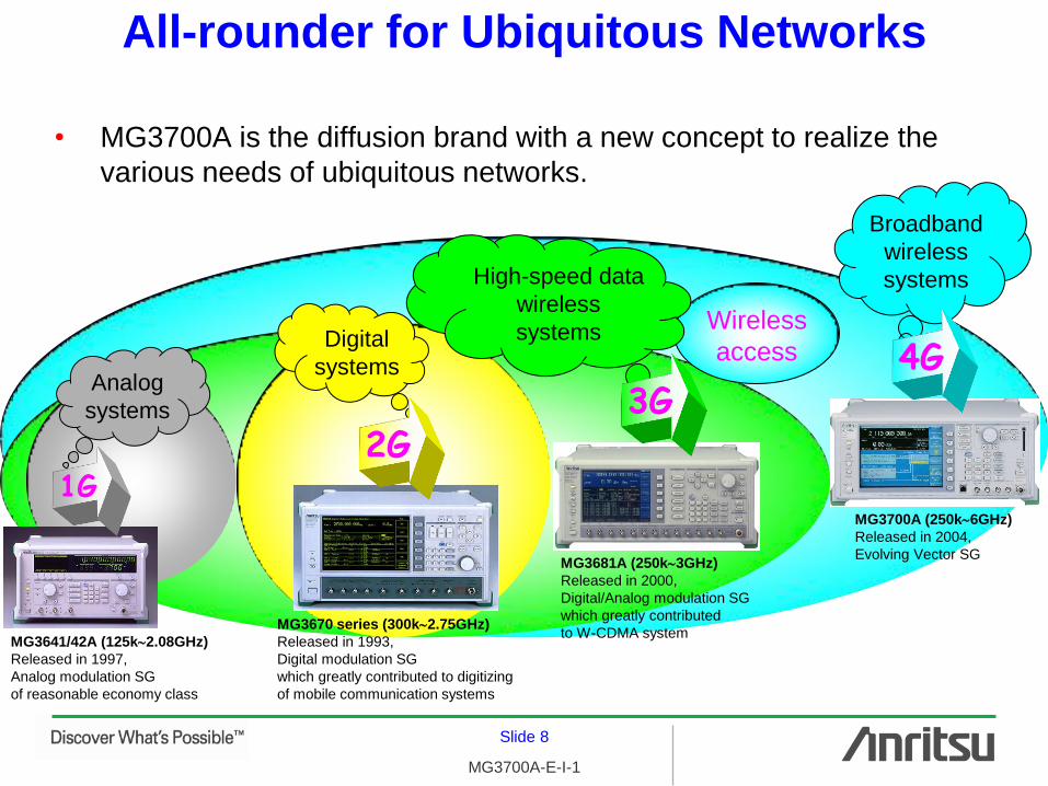
MG3700A-E-I-1
• MG3700A is the diffusion brand with a new concept to realize the
various needs of ubiquitous networks.
All-rounder for Ubiquitous Networks
Digital
systems
2G
MG3670 series (300k2.75GHz)
Released in 1993,
Digital modulation SG
which greatly contributed to digitizing
of mobile communication systems
MG3681A (250k3GHz)
Released in 2000,
Digital/Analog modulation SG
which greatly contributed
to W-CDMA system
Analog
systems
1G
MG3641/42A (125k2.08GHz)
Released in 1997,
Analog modulation SG
of reasonable economy class
Wireless
access
Broadband
wireless
systems
MG3700A (250k6GHz)
Released in 2004,
Evolving Vector SG
High-speed data
wireless
systems
3G 4G

Slide 9
MG3700A-E-I-1
Wideband Modulation Capability Adaptable Up to 4G
• NTT DoCoMo started development of the next generation mobile
communication system for which utilization is expected by 2010.
• High-speed packet data communications with maximum 2.5 Gbps
downlink and maximum 20 Mbps uplink were achieved.
Source: NTT DoCoMo
Experimental
Base Station
Experimental
User Equipment
(in-car)
Downlink
Uplink
f
100MHz bandwidth is divided into 768 carriers, and it transmits in parallel.
VSF-Spread OFDM: Variable Spreading Factor Spread Orthogonal Frequency Division Multiplexing
MIMO: Multiple-Input-Multiple-Output
VSF-Spread OFDM signal
Signal of user 2
Signal of user 1
Signal spread by
user-specific SF
Wireless technology Downlink Uplink
Radio access scheme VSF-Spread OFDM & MIMO VSF-CDMA
Bandwidth 101.5 MHz 40 MHz
Number of sub-carrier 768 (131.836 kHz spacing) 2 (20 MHz spacing)
OFDM symbol length 9.259 ms -
Guard interval length 1.674 ms -
Frame length 0.5 ms 0.5 ms
Data modulation scheme QPSK, 16QAM, 64QAM QPSK, 16QAM, 64QAM
Channel coding (Rate) Turbo coding (1/3 ~ 8/9) Turbo coding (1/3 ~ 1/16)
Spreading factor 1 ~ 128 1 ~ 256

Slide 10
MG3700A-E-I-1
» Simulation using FFT
Wideband Modulation Capability Adaptable Up to 4G
• Spectrum
Slide 11
MG3700A-E-I-1
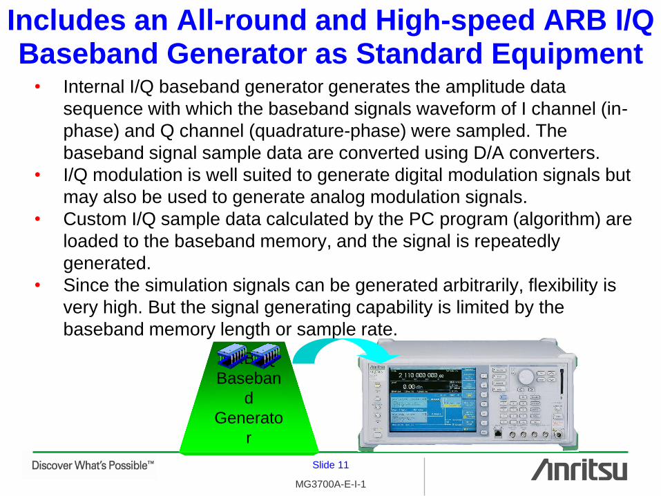
Includes an All-round and High-speed ARB I/Q Baseband Generator as Standard Equipment
• Internal I/Q baseband generator generates the amplitude data
sequence with which the baseband signals waveform of I channel (in-
phase) and Q channel (quadrature-phase) were sampled. The
baseband signal sample data are converted using D/A converters.
• I/Q modulation is well suited to generate digital modulation signals but
may also be used to generate analog modulation signals.
• Custom I/Q sample data calculated by the PC program (algorithm) are
loaded to the baseband memory, and the signal is repeatedly
generated.
• Since the simulation signals can be generated arbitrarily, flexibility is
very high. But the signal generating capability is limited by the
baseband memory length or sample rate.
ARB IQ
Baseban
d
Generato
r

Slide 12
MG3700A-E-I-1
Includes Baseband Memory and Hard Disk that Store Large-volume Baseband Signal Data as Standard
Equipment • Baseband memory
» Memory for generating I/Q
sample data
Dual Baseband memory
• Hard disk drive (HDD) » Hard disk for saving the
signal pattern files which
consist of I/Q sample data
files and signal configuration
files
• CompactFrash (CF) » Removable media
ARB IQ
Baseband
Generator
Max. 2 256 Msample/channel (with Memory upgrade option)
HDD
40 GB

Slide 13
MG3700A-E-I-1
Includes BER Analyzer Required for Receiver Sensitivity Test as Standard Equipment
• Receiver sensitivity test can measure error rate specified by BER. » W-CDMA, GSM, PHS, PDC etc.
• A BERT (Bit Error Rate Tester) installed as standard equipment
contributes to easy receiver testing and space saving.
Mounted BERT

Slide 14
MG3700A-E-I-1
Fast Switching, High Reliability
• Fast testing and high reliability are critical specifications for Auto Test
Equipment (ATE). » Fast switching
– Original frequency synthesizer technique has balanced of cost and
performance.
– Fast switching time employing an electronic step attenuator improves test
throughput.
» High reliability – MTBF has been improved employing an electronic step attenuator instead
of the traditional mechanical step attenuator.
» Free application drivers – National Instruments LabView drivers save time and money in code
generation and maintenance. – The driver can be downloaded free from the Anritsu MG3700A website.
ME7856A RFIC Tester
with three MG3700As

Slide 15
MG3700A-E-I-1
High Level Accuracy
• Output level accuracy leading to the repeatability of measurement
data is a critical specification in order to control the uncertainty of
measured values. – Output level accuracy is derived from the uncertainty of calibrating
instruments, repeatability of ALC (Automatic Level Control), repeatability of
step attenuator, flatness, and impedance mismatch.
» The new automatic fast-acting internal calibration routine executed
quickly achieves high level accuracy 0.5 dB. * CW, 23 5 C – Level error between I/Q modulation and CW 0.2 dB
» The ability to set output level by 0.01 dB resolution in all output level
ranges is useful to improve receiver test accuracy and to adjust level
little by little.

Slide 16
MG3700A-E-I-1
Ethernet Remote Operation to Make Maintenance Management Easy
• ATE or multiple-instrument deployment can be operated efficiently by
management through the network. » Remote operation
– Ethernet control same as GPIB control
(Raw Socket interface)
» File transfer between internal HDD and PC – Transfer with FTP using the instrument accessory PC software (2 MB/s)
LAN
RTOS: VxWORKS

Slide 17
MG3700A-E-I-1
Weight Saving to Increase Mobility
• Weight saving increases mobility for field test usage and for shared
instruments that moves frequently to installation sites.
• 10 kg lighter than traditional instruments » Meets new needs
15 kg

Slide 18
MG3700A-E-I-1
Ecological Design
• Excellent Eco Product • This symbol indicates Anritsu products with industry-leading environmental
friendliness, enough transparency to disclose such information, and conformance
to environment-friendly criteria uniquely set by Anritsu. Anritsu is now promoting
the development of environment-friendly products which impose less burden on
the environment throughout their life cycles (procurement of materials,
manufacturing,distribution, use, and disposal).
• Low power consumption » Energy saving: 2/3 of power consumption compared to previous type.
– 200 VA
• Standby power consumption virtually zero » Standby state has been abolished by employing a reference oscillator
with excellent start-up characteristic. – “Main Power” LED lighting only
• Pb-free soldering » Toxic lead substances are not used.
• Weight saving » Curtails the use of raw material and improves distribution efficiency.

Slide 19
MG3700A-E-I-1
All-round Applications
• Since standard signal pattern files for major applications are saved to
the internal HDD, major signals can be generated immediately after
obtaining MG3700A.
Lineup of Standard Signal Pattern files
– WLAN (IEEE802.11a/b/g)
– W-CDMA
– GSM/EDGE
– CDMA2000 1xEV-DO (Rev.0)
– CDMA2000 1X
– PHS
– PDC
– Bluetooth
– GPS
– Digital Broadcast
Option – TD-SCDMA
HDD

Slide 20
MG3700A-E-I-1
All-round Applications
• PC-based Windows simulation software "IQproducer" optimized to
specific application can be provided in order to generate signal
pattern files, so signal patterns can be customized.
License option IQproducer
– HSPA over W-CDMA
– Universal TDMA
– CDMA2000 1xEV-DO (Rev.0)
– Multi-carrier
– Mobile WiMAX
– DVB-T/H
– Fading
– 3GPP LTE
No license (Standard)
IQproducer – Limited W-CDMA
– AWGN
FTP
Creating Signal
Pattern files
Editing
Signal Pattern
NEW
NEW
Slide 21
MG3700A-E-I-1
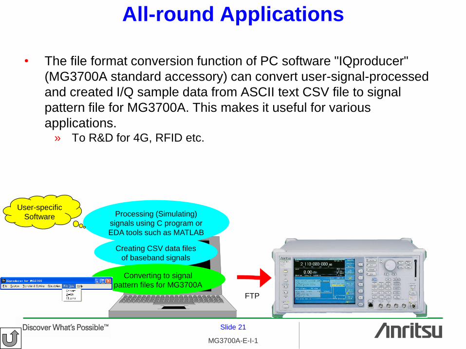
All-round Applications
• The file format conversion function of PC software "IQproducer"
(MG3700A standard accessory) can convert user-signal-processed
and created I/Q sample data from ASCII text CSV file to signal
pattern file for MG3700A. This makes it useful for various
applications. » To R&D for 4G, RFID etc.
Creating CSV data files
of baseband signals
Processing (Simulating)
signals using C program or
EDA tools such as MATLAB
Converting to signal
pattern files for MG3700A
FTP
User-specific
Software

Slide 22
MG3700A-E-I-1
Features
• Product Outline
• Features » Instrument
Platform
» Software
• Options
• Block Diagram 23
• Connectivity 25
• High Level Accuracy 27
• High Spectral Purity 34
• Wideband I/Q Modulation 56
• I/Q Adjustment,
Differential I/Q Output 60
• Advanced High-speed
I/Q Baseband 63
• BER Analyzer 83
• Operability 85
• Remote Operation 89
• Radiated Interference
Leakage 91
• Maintainability 92

Slide 23
MG3700A-E-I-1
INT
EXT
Overall Block Diagram
I/Q
Baseband
Generator ALC
I/Q
Modulator
I Q Q I I Q
Pulse
Modulator
Step
Attenuator
2
100 MHz
Reference
8
YTO
4.8 8 GHz
RF
Pulse
INT
EXT
Burst gate control
- ele
ctr
onic
- M
echanic
al (O
ption
)
D/A
Amplitude Amplitude
D/A
4 GHz
I
Q
250 k 3 GHz
3< 6 GHz
(Option)
DC
offset
DC
offset

Slide 24
MG3700A-E-I-1
Baseband Block Diagram
to I/Q
Modulator
to I/Q
Modulator
Sampling rate 400 MHz
(Internal interpolation)
2 128Msample/channel
2 256Msample/channel (Option)
Baseband
memory B
14 bits
Baseband
memory A
or
Sequence
D/A
D/A
100 kHz
300 kHz
1 MHz
3 MHz
10 MHz
30 MHz
70 MHz
Through
DDS
INT EXT
16,8,4,2,1,1/2,1/4,1/8,1/16
Sample Clock 20 k 160 MHz
f Gain
Amplitude
-8 8 dB
A/B 80 dB
Calibration
source
t
Interpolator
Upsample Clock 160 MHz
Gain
I
Q
Baseband Reference Clock
20 k 40 MHz
100 MHz
Reference

Slide 25
MG3700A-E-I-1
Connectivity Front Panel
100Base-TX
External frame synchronizing trigger External I/Q Input
RF Output
(N connector)
Sequence controlling trigger
Slide 26
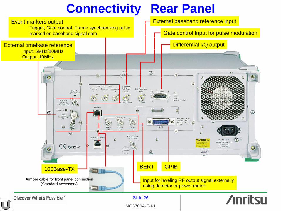
MG3700A-E-I-1
Connectivity Rear Panel
External timebase reference Input: 5MHz/10MHz
Output: 10MHz
Event markers output Trigger, Gate control, Frame synchronizing pulse
marked on baseband signal data Gate control Input for pulse modulation
100Base-TX
Input for leveling RF output signal externally
using detector or power meter
Differential I/Q output
External baseband reference input
BERT GPIB
Jumper cable for front panel connection
(Standard accessory)
Slide 27
MG3700A-E-I-1
High Level Accuracy
• Automatic internal calibration routine » The reference source for internal calibration automatically calibrates at
high-speed from DAC to ALC Loop. – When the change of frequency, output level, and I/Q RMS level (Signal
pattern selection) • The switching time of frequency and output level includes automatic calibration.
» The detector performance of ALC Loop was improved.
• Correction at high resolution per unit » The frequency response, the linearity error of ALC circuitry, and the
attenuation error of the step attenuator are measured using the
ML2437A/38A Power Meter and the ML2530A Calibration Receiver with
wide dynamic range and high linearity, and then the data is inputted to
correction table.
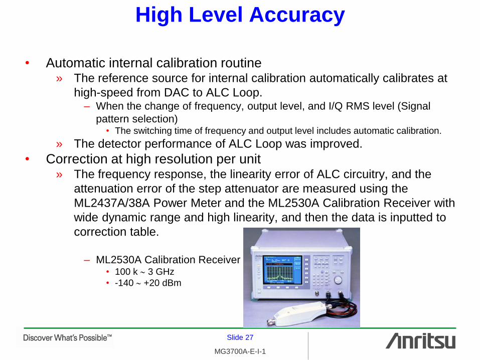
– ML2530A Calibration Receiver
• 100 k 3 GHz
• -140 +20 dBm

Slide 28
MG3700A-E-I-1
• Frequency response » CW
Limits (23 5 C)
» 0.5 dB * 25 M 3 GHz – -120 +6 dBm
– -120 +10 dBm * with Option
Mechanical attenuator
Typical Level Accuracy
• Linearity » CW
– Relative level accuracy
Initial power -11 [dBm] E-ATT
Limits (23 5 C)
» 0.2 dB typ. * 25 M ~ 3 GHz
» 0.3 dB typ. * 3 ~ 6 GHz – -120 -11 dBm
– -120 -7 dBm * with Option
Mechanical attenuator
-0.5
-0.4
-0.3
-0.2
-0.1
0
0.1
0.2
0.3
0.4
0.5
0 1000 2000 3000 4000 5000 6000
Frequency [MHz]
Po
we
r e
rro
r [d
B]
E-ATT: -11 [dBm]
-0.4
-0.3
-0.2
-0.1
0
0.1
0.2
0.3
0.4
-140 -120 -100 -80 -60 -40 -20 0
Output Level [dBm]P
ow
er
err
or
[dB
] 1 GHz
2 GHz
3 GHz
4 GHz
5 GHz
6 GHz

Slide 29
MG3700A-E-I-1
Typical Level Stability
• Aging » CW (ALC: Active)
– 1 GHz, -11 dBm
» Difference 0.035 dB -0.063 -0.028 dB
• Aging » Level continuous mode,
I/Q modulation (ALC: Hold) – 1 GHz, -11 dBm,
W-CDMA UL RMC 12.2kbps
» Difference 0.21 dB -0.069 0.141 dB
-0.1
-0.09
-0.08
-0.07
-0.06
-0.05
-0.04
-0.03
-0.02
-0.01
0
0 2 4 6 8 10 12 14 16 18 20 22 24
Elapsed time [hours]
Pow
er
err
or
[dB
]
-0.2
-0.15
-0.1
-0.05
0
0.05
0.1
0.15
0.2
0 2 4 6 8 10 12 14 16 18 20 22 24
Elapsed time [hours]
Pow
er
err
or
[dB
]

Slide 30
MG3700A-E-I-1
Typical Level Stability
• RF off on (off [on] off [on] ...) » CW
– 2 GHz, -11 dBm
» Difference 0.017 dB -0.007 0.01 dB
• RF off on (off [on] off [on] ...) » I/Q modulation
– 2 GHz, -11 dBm, W-CDMA
» Difference 0.022 dB -0.012 0.01 dB
-0.05
-0.04
-0.03
-0.02
-0.01
0
0.01
0.02
0.03
0.04
0.05
0 50 100 150 200
Elapsed count
Pow
er
err
or
[dB
]
-0.05
-0.04
-0.03
-0.02
-0.01
0
0.01
0.02
0.03
0.04
0.05
0 50 100 150 200
Elapsed count
Pow
er
err
or
[dB
]

Slide 31
MG3700A-E-I-1
Typical Level Stability
• I/Q Modulation CW
(Mod on [off] on [off] ...) – 2 GHz, -11 dBm, W-CDMA
» Difference 0.017 dB -0.009 0.008 dB
• CW I/Q Modulation
(Mod off [on] off [on] off ...) – 2 GHz, -11 dBm, W-CDMA
» Difference 0.023 dB -0.011 0.012 dB
-0.05
-0.04
-0.03
-0.02
-0.01
0
0.01
0.02
0.03
0.04
0.05
0 50 100 150 200
Elapsed count
Pow
er
err
or
[dB
]
-0.05
-0.04
-0.03
-0.02
-0.01
0
0.01
0.02
0.03
0.04
0.05
0 50 100 150 200
Elapsed count
Pow
er
err
or
[dB
]

Slide 32
MG3700A-E-I-1
Typical Level Stability
• Random level [-140 -1 dBm] -11 dBm
(any level [-11] any level [-11] ...) – 2 GHz, I/Q Modulation (W-CDMA)
» Difference 0.023 dB -0.011 0.012 dB
-0.05
-0.04
-0.03
-0.02
-0.01
0
0.01
0.02
0.03
0.04
0.05
0 50 100 150 200
Elapsed count
Pow
er
err
or
[dB
]

Slide 33
MG3700A-E-I-1
Typical Maximum Available Output Level
• Electronic step attenuator (Standard): +13 dBm setting – E-ATT
• Mechanical step attenuator (Option): +19 dBm setting – M-ATT
8
10
12
14
16
18
20
0 1000 2000 3000 4000 5000 6000
Frequency [MHz]
Outp
ut
Pow
er
[dB
m]
E-ATT M-ATT

Slide 34
MG3700A-E-I-1
High Spectral Purity
What type of specification are there for spectral purity?
• Spurious » Harmonics
– 2 fc
– 3 fc
» Non-harmonics – Local Oscillator (LO) leakage: fLO
– Image signal: fimg
– IF signal leakage: fIF
– Mixing signal of Harmonic IF and LO: 2 fIF - fLO
» Sub-harmonics None – 1/2 fc, 3/2 fc
» Power line and Fan rotation (Hum) – fc Harmonics of AC frequency (especially 3rd order)

Slide 35
MG3700A-E-I-1
High Spectral Purity
What type of specification are there for spectral purity?
• SSB Single Side Band phase noise » Phase noise of Reference oscillator (100 MHz) ... (a)
» Loop bandwidth of PLL Phase Locked Loop ... (b)
» Phase noise of YTO YIG Tuned Oscillator ... (c)
» Noise floor ... (d)
fc
(d)
(a)
(b)
(c)
Power spectrum
Noise level in 1 Hz bandwidth
to carrier level
(dBc/Hz)
Offset frequency (log scale)

Slide 36
MG3700A-E-I-1
Spurious
• 4.8 - 8 GHz YTO has been employed as LO. And LO, image signal
and IF leakage were placed out of the range of output frequency. fc LO frequency Image frequency IF
– 250 kHz 3 GHz: fc + 4.8 GHz fc + 9.6 GHz 4.8 GHz
– 3 GHz < 6 GHz : fc + 8.8 GHz fc + 17.6 GHz 8.8 GHz
LO(fLO)
IF(fIF) RF(fc)
fLO
f
fc
fimg
f
fIF fIF
fIF
f 2 fIF
2 fIF - fLO fLO
Overlap on
2.4 GHz (fc 3 GHz)
4.4 GHz (fc > 3 GHz)
fIF
Be careful
Distortion by Mixer
Frequency down conversion
Slide 37
MG3700A-E-I-1
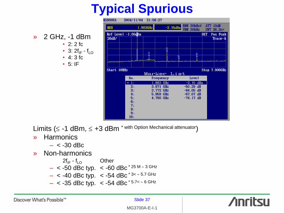
Typical Spurious
» 2 GHz, -1 dBm • 2: 2 fc
• 3: 2fIF - fLO
• 4: 3 fc
• 5: IF
Limits ( -1 dBm, +3 dBm * with Option Mechanical attenuator)
» Harmonics – < -30 dBc
» Non-harmonics 2fIF - fLO Other
– < -50 dBc typ. < -60 dBc * 25 M 3 GHz
– < -40 dBc typ. < -54 dBc * 3< 5.7 GHz
– < -35 dBc typ. < -54 dBc * 5.7< 6 GHz

Slide 38
MG3700A-E-I-1
SSB Phase Noise
In wireless communication, in order to utilize limited radio resources
effectively, there is a strong phase noise requirement for signal
sources. » Alternate channel leakage power ratio which spaces one channel from
adjacent channel is caused by phase noise.
• Optimization of cost performance » The balance between cost and performance was optimized, meeting
present needs.
» A high-speed 14-bit DAC that interpolates internally to a maximum 400
MHz sampling rate has been employed, and the quantization noise
leading to residual noise was reduced.
» A smoothing filter with variable cutoff frequency according to the
modulation bandwidth eliminates alias spurious and noise.
• Employed high-purity YTO » Although the YTO employed as a LO is expensive, it provides all-round
performance by simplifying the circuitry.

Slide 39
MG3700A-E-I-1
Selectable Frequency Switching Time and Phase Noise
• Frequency switching time affects the phase noise.
• The frequency switching time and phase noise profile is changed by
switching the loop bandwidth of the PLL synthesizer. It is useful to
select it according to the wireless system or the usage.
fc 50kHz 1MHz
Normal
Fast
Normal Fast
Frequency switching time 3 GHz
non-cross
3 GHz
cross
3 GHz
Non-cross
3 GHz
cross
f < 1 GHz f 1 GHz
Electronic attenuator 15 ms 20 ms 40 ms 10 ms 40 ms
Mechanical attenuator 80 ms 100 ms 80 ms 100 ms
Phase noise Lower in Offset frequency 50 kHz Lower in Offset frequency < 50 kHz
Slide 40
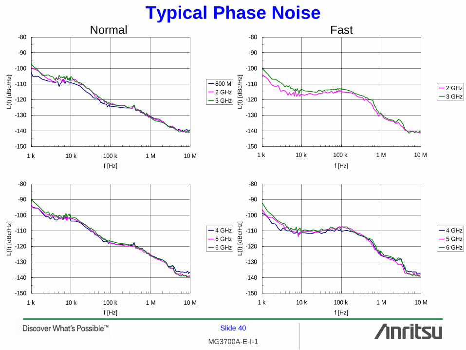
MG3700A-E-I-1
Typical Phase Noise Normal Fast
-150
-140
-130
-120
-110
-100
-90
-80
1000 10000 100000 1000000 10000000
f [Hz]
L(f
) [d
Bc/H
z]
800 M
2 GHz
3 GHz
10 M1 M100 k10 k1 k
-150
-140
-130
-120
-110
-100
-90
-80
1000 10000 100000 1000000 10000000
f [Hz]
L(f
) [d
Bc/H
z]
4 GHz
5 GHz
6 GHz
10 M1 M100 k10 k1 k
-150
-140
-130
-120
-110
-100
-90
-80
1000 10000 100000 1000000 10000000
f [Hz]
L(f
) [d
Bc/H
z]
2 GHz
3 GHz
10 M1 M100 k10 k1 k
-150
-140
-130
-120
-110
-100
-90
-80
1000 10000 100000 1000000 10000000
f [Hz]
L(f
) [d
Bc/H
z]
4 GHz
5 GHz
6 GHz
10 M1 M100 k10 k1 k

Slide 41
MG3700A-E-I-1
Adjacent Channel Leakage Power Ratio (ACLR)
In wireless communication, in order to utilize limited radio resources
effectively, there is a strong ACLR requirement for signal sources. » It is a critical specification for reference signal sources evaluating
transmitter components/devices and for interference signal sources
testing receivers.
» Adjacent channel leakage power ratio of modulated signals is caused
by intermodulation distortion produced by nonlinear elements in signal
generator.
• ACLR specification 800 1000 MHz, 1800 2400 MHz, 23 5C,
W-CDMA Downlink (Test Model 1 64 DPCH) With Option Mechanical attenuator
» 5 MHz offset: -61 dB -62 dB • Output level -4 dBm 0 dBm
» 10 MHz offset: -66 dB typ. -67 dB typ. • Output level -1 dBm +3 dBm
– Alternate channel leakage power ratio is caused by phase noise.
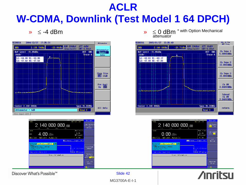
Slide 42
MG3700A-E-I-1
ACLR W-CDMA, Downlink (Test Model 1 64 DPCH)
» -4 dBm » 0 dBm * with Option Mechanical
attenuator
Slide 43
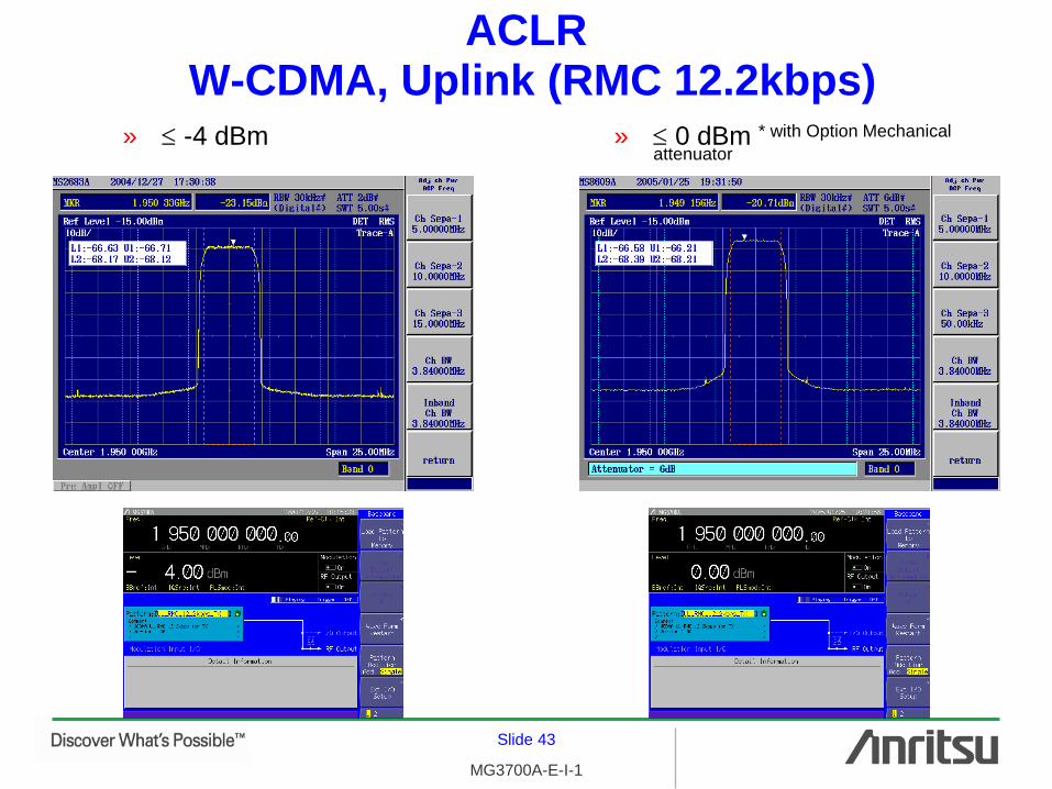
MG3700A-E-I-1
ACLR W-CDMA, Uplink (RMC 12.2kbps)
» -4 dBm » 0 dBm * with Option Mechanical
attenuator

Slide 44
MG3700A-E-I-1
ACLR W-CDMA, Downlink (TM1 64DPCH), 4 Carriers
» -4 dBm
» 0 dBm * with Option Mechanical
attenuator

Slide 45
MG3700A-E-I-1
Spurious Close to Carrier CDMA2000 1X, Forward (RC1-2)
» -4 dBm » 0 dBm * with Option Mechanical
attenuator

Slide 46
MG3700A-E-I-1
Spurious Close to Carrier CDMA2000 1X, Forward (RC3-5)
» -4 dBm » 0 dBm * with Option Mechanical
attenuator

Slide 47
MG3700A-E-I-1
Spurious Close to Carrier CDMA2000 1X, Reverse (RC1-2)
» -4 dBm » 0 dBm * with Option Mechanical
attenuator

Slide 48
MG3700A-E-I-1
Spurious Close to Carrier CDMA2000 1X, Reverse (RC3-4)
» -4 dBm » 0 dBm * with Option Mechanical
attenuator

Slide 49
MG3700A-E-I-1
Spurious Close to Carrier CDMA2000 1xEV-DO, Forward (Active Slot)
» -4 dBm » 0 dBm * with Option Mechanical
attenuator
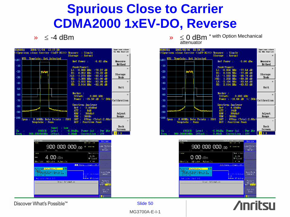
Slide 50
MG3700A-E-I-1
Spurious Close to Carrier CDMA2000 1xEV-DO, Reverse
» -4 dBm » 0 dBm * with Option Mechanical
attenuator
Slide 51
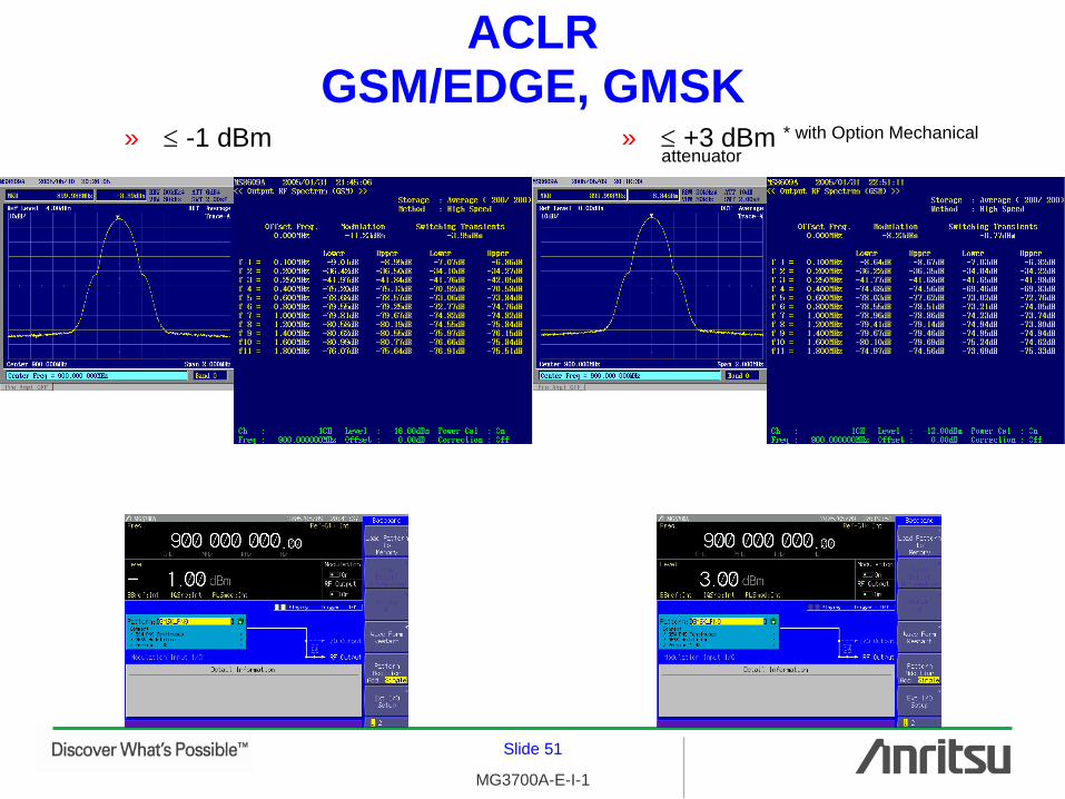
MG3700A-E-I-1
ACLR GSM/EDGE, GMSK
» -1 dBm » +3 dBm * with Option Mechanical
attenuator

Slide 52
MG3700A-E-I-1
ACLR GSM/EDGE, 8PSK
» -1 dBm » +3 dBm * with Option Mechanical
attenuator

Slide 53
MG3700A-E-I-1
» -1 dBm » +3 dBm * with Option Mechanical
attenuator
ACLR PHS

Slide 54
MG3700A-E-I-1
» -1 dBm » +3 dBm * with Option Mechanical
attenuator
ACLR PDC

Slide 55
MG3700A-E-I-1
» -4 dBm » 0 dBm * with Option Mechanical
attenuator
ACLR WLAN IEEE 802.11a

Slide 56
MG3700A-E-I-1
Wideband I/Q Modulation
Modulation bandwidth using internal I/Q
Bandwidth Flatness 3 GHz > 3 GHz
• 20 MHz (10 MHz) < 0.5 dB (0.2 GHz) < 1 dB
• 120 MHz (60 MHz) < 2 dB (1 GHz) < 3 dB
-5
-4
-3
-2
-1
0
1
-60 -40 -20 0 20 40 60
Frequency offset from carrier [MHz]
[dB
] 1 GHz
2 GHz
3 GHz
-5
-4
-3
-2
-1
0
1
-60 -40 -20 0 20 40 60
Frequency offset from carrier [MHz]
[dB
]
3.1 GHz
4 GHz
5 GHz
6 GHz

Slide 57
MG3700A-E-I-1
Wideband I/Q Modulation
Modulation bandwidth using external I/Q
Bandwidth Flatness 3GHz > 3GHz
• 20 MHz (10 MHz) < 0.5 dB (0.2 GHz) < 1 dB
• 150 MHz (75 MHz) < 3 dB (1 GHz) < 5 dB
• 200 MHz (100 MHz) < 6 dB (1 GHz) < 9 dB
-5
-4
-3
-2
-1
0
1
-100 -80 -60 -40 -20 0 20 40 60 80 100
Frequency offset from carrier [MHz]
[dB
] 1 GHz
2 GHz
3 GHz
-5
-4
-3
-2
-1
0
1
-100 -80 -60 -40 -20 0 20 40 60 80 100
Frequency offset from carrier [MHz]
[dB
]
3.1 GHz
4 GHz
5 GHz
6 GHz

Slide 58
MG3700A-E-I-1
External I/Q Input
• It is possible to output RF by inputting external I/Q baseband signals. » Full scale Input (Optimum level):
• Setting
VrmsQI 5.022

Slide 59
MG3700A-E-I-1
Carrier Leakage
• The leakage of the carrier inputted into I/Q modulator stays in RF
signal. » It is quantified by origin offset of signal constellation.
» It deteriorates quality of the modulation and causes problems for
receiver tests.
• Since the leakage adjusted to the minimum level is stable, its
subsequent tune-up is unnecessary. » -40 dBc
Typical
Shift
DAC
DAC
LPF
fc
I
Q
Clock
Carrier
/2
fc
fck
I/Q modulation Block diagram

Slide 60
MG3700A-E-I-1
I/Q Adjustment and Differential I/Q Output
• In order to test I/Q modulators, I/Q adjustment and differential
(balanced) outputs of I,I, Q,Q are required for the signal source. » Vector magnitude
– Amplitude voltage is set as RMS level of I/Q modulator.
» Drive DC voltage – In order to drive I/Q modulator for the single power source, DC offset is set
as drive voltage.
• In order to test I/Q modulators and baseband LSI for balanced
devices, I,I, Q,Q differential (balanced) outputs are required for the
signal source. » In I/Q input device, the balanced input has the advantage which can
reduce the amplitude error and noise compared with I and Q
unbalanced (single-ended) inputs. – Reduction of amplitude error by the ground loop
• The cause is that the grounds of signal source and input device are not equivalent
potential.
– Reduction of signal line noise • The cause is that the environmental noise is picked up on the signal line.

Slide 61
MG3700A-E-I-1
I/Q Output
• Differential I/Q signals can be outputted. » I /Q signals which are reverse signals (amplitude is equal and polarity
is reverse) of I/Q signals are outputted. – D-Sub 15 (Jack), 50
J1277 (Optional accessory)
D-Sub>BNC adapter
• Setting

Slide 62
MG3700A-E-I-1
I/Q Adjustment
• Variable of amplitude voltage of I/Q signals outputs, DC offset » Amplitude voltage
– 0 120%, Resolution 0.1%
» DC offset – I /I, Q /Q common offset: -1 +3 V, Resolution 10 mV
– I /I, Q /Q differential offset: -50 +50 mV, Resolution 0.05 mV
» Amplitude voltage range – Amplitude voltage Common DC offset Differential DC offset:
-3.5 +3.5 V Q
I +1 V
+1 V
Voltage [V]
0 t
Common DC offset
I / Q
I /Q
+3.5
Differential DC offset
Amplitude voltage
Upper Limit
I /Q DC offset: Common DC offset - Differential DC offset /2
I / Q DC offset: Common DC offset + Differential DC offset /2
22 QI
22 QI
Slide 63
MG3700A-E-I-1
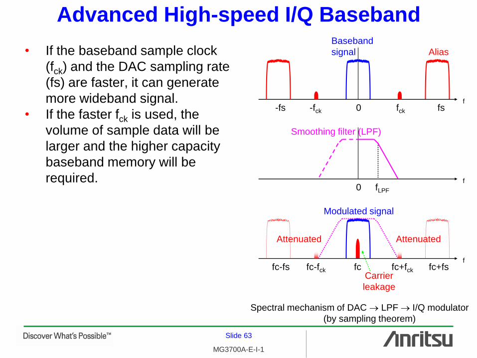
Advanced High-speed I/Q Baseband
• If the baseband sample clock
(fck) and the DAC sampling rate
(fs) are faster, it can generate
more wideband signal.
• If the faster fck is used, the
volume of sample data will be
larger and the higher capacity
baseband memory will be
required.
f
f
f
-fs 0
0
fc-fs fc
Baseband
signal
fLPF
Alias
Modulated signal
Attenuated
Carrier
leakage
Smoothing filter (LPF)
fs
fc+fs
Spectral mechanism of DAC LPF I/Q modulator
(by sampling theorem)
fck -fck
fc+fck fc-fck
Attenuated

Slide 64
MG3700A-E-I-1
High-speed I/Q Baseband
• Sample rate (Fs) » 20 k 160 MHz, Resolution 0.001 Hz
• Upsample clock (fck) » fck = 2n Fs 160 MHz (n: maximum integer)
– at Fs 20 MHz
» Automatic interpolation – Interpolator upsamples the sample clock (fck) to the maximum, and fck is
further kept away from modulated signal frequency.
• DAC Sampling rate (fs) » 400 MHz
– Since the internal interpolation DAC was employed, alias is further kept
away from modulated signal frequency.
» Automatic interpolation fs – 20 < fck 50 MHz: 8 fck
– 50 < fck 100 MHz: 4 fck
– 100 < fck 160 MHz: 2 fck

Slide 65
MG3700A-E-I-1
Dual Baseband Memory
• High-capacity baseband memory can generate high-speed signals
and long term signals » 2 128 Msample/channel (1 GB)
» 2 256 Msample/channel (2 GB) * with Option Memory upgrade – The flash memory had been mainly employed. But since DRAM used for the
main memory in PC was employed, the cost was reduced in spite of high-
capacity and fast-loading.
Channel Event
I , Q (, Marker 1, Marker 2, Marker 3, RF Gate)
Maximum of
256,000,000 sample
512,000,000 sample * with Option
Sample data generates in sample time Ts=1/Fs

Slide 66
MG3700A-E-I-1
Dual Baseband Memory
• Able to generate two signals which mixed digitally the signals of the
baseband memories A and B. » Two signals which mixed the signals of different sample rate (Fs)
cannot be generated correctly. – MX370104A Multi-carrier IQproducer can adjust different Fs.
– e.g. W-CDMA + GSM, IEEE 802.11a/g + 802.11b/g
» Two signals which mixed DL RMC signal for W-CDMA UE receiver test
with full SFN count, and interference signal or AWGN cannot be
generated.
» Two signals which mixed DL RMC 12.2 kbps signal for W-CDMA UE
receiver test with limited SFN count, and interference signal or AWGN
can be generated.
A
B
P-CCPCH 4096 frames with full SFN 11 bit count (0 2047)
DL channel without P-CCPCH CPICH, P-SCH, S-SCH, PICH,
DPCH, OCNS,
HS-SCCH, HS-PDSCH
DL RMC with full SFN count
A
B
DL RMC 12.2 kbps 1022 frames with limited SFN 11 bit count (0 510)
Interference signal, AWGN
Two signals
Two signals
Interference signal, AWGN
Restriction
Restriction

Slide 67
MG3700A-E-I-1
Dual Baseband Memory
• The signals output level of memories A and B can be set as [dBm]
and [dB]. » A/B level ratio: 0 80 dB, Resolution 0.01 dB
• Frequency offset (f) is available. – Shift the A frequency
• Carrier leakage stays on the B frequency.
» 0 (0.8 Fs 2n - Bandwidth)/2 – at Fs 20 MHz
– 2n Fs 160 MHz (n: maximum integer)
» 0 (0.8 Fs - Bandwidth)/2 – at Fs > 20 MHz
– Bandwidth: Modulation rate[cps, sps] = Fs/Oversampling ratio
• Example of W-CDMA: (0.8 4 3.84 MHz 23 - 3.84 MHz)/2 = 47.232 MHz
» Resolution 1 Hz
• Timing offset (t) is available. » 0 (Total sample of A - 1) 9,999,999 , Resolution 1 sample
– Shift the B start timing • It is useful to the signals with same A and B, such as multipath and TX diversity.
Slide 68
MG3700A-E-I-1
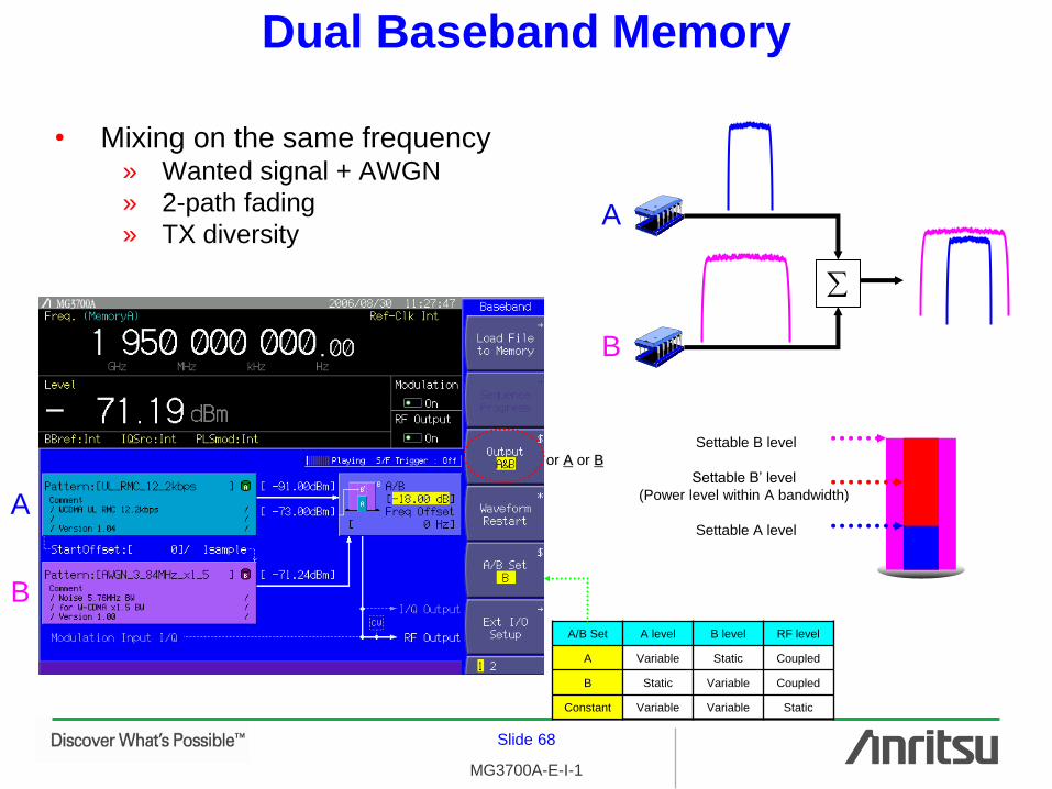
Dual Baseband Memory
• Mixing on the same frequency » Wanted signal + AWGN
» 2-path fading
» TX diversity
Settable A level
Settable B level
Settable B’ level
(Power level within A bandwidth)
A
B
B
A
or A or B
A/B Set A level B level RF level
A Variable Static Coupled
B Static Variable Coupled
Constant Variable Variable Static

Slide 69
MG3700A-E-I-1
Dual Baseband Memory
• Mixing on different frequency » Wanted signal + Interference signal or CW
» AWGN + AWGN
Settable A level
Settable B level
Settable Frequency offset
A
B
Set Frequency
B
A
or A or B
A/B Set A level B level RF level
A Variable Static Coupled
B Static Variable Coupled
Constant Variable Variable Static

Slide 70
MG3700A-E-I-1
• Baseband memories A and B load the I/Q sample data in the saved
signal pattern files from HDD in advance. » Loading time: 14 MB/s (7 MS/s)
» Maximum package/baseband memory: 100
» Maximum pattern/package: 100
» Maximum pattern/baseband memory: 4,096
» Minimum sample/pattern: 1,000
• Baseband memories A and B output I/Q sample data of the selected
signal pattern.
Dual Baseband Memory
Package 2
Pattern 21
Pattern 22
Pattern 23
Package 1
Pattern 11
Pattern 12
Pattern 13
Package 3
Pattern 31
Pattern 32
Pattern 33
Package 4
Pattern 41
Pattern 42
Pattern 43
Baseband
memory B
Baseband
memory A
Package 2
Pattern 21
Package 1
Pattern 11
Pattern 12
Pattern 13
Package 2
Pattern 21
Package 4
Pattern 41
Pattern 43
Pattern 41 Pattern 12 Output
Folder
Signal pattern file HDD

Slide 71
MG3700A-E-I-1
Dual Baseband Memory
• When outputting long term signals with larger capacity than
baseband memory A, the memories of A and B are combined
automatically. » Simulated signal pattern of fading
» Real signal pattern for receiving video and voice test
• W-CDMA 16.66 s (1,666 frame)
33.33 s * with Memory upgrade option – Sample rate (Fs): 4 3.84 Mcps
• VSF-Spread OFDM roughly 4 s * with Memory upgrade option
A+B

Slide 72
MG3700A-E-I-1
Dual Baseband Memory
• When a long term signal is loaded to a baseband memory, all the
memorized patterns are deleted. » Maximum pattern/baseband memories A+B: 1
– The message is displayed when downloading in a baseband memory (A).

Slide 73
MG3700A-E-I-1
Sequence/Combination of Signal Patterns
• The signal pattern sequence can be generated. » Useful to protocol emulation
» Available for digital sweep of output level
• Shortcut operation is served. » Simplification of operation for combination output
» Management of utilized pattern files in custom packages
• The combination files can be created/defined by PC software "IQ producer"
(standard accessory).
Package 1
Pattern 11
Pattern 12
Pattern 21 Pattern 11
Sequence output
HDD
… Pattern 12 … Pattern 22
Combination output
Custom Package
Combination 1
Package 1
Pattern 11
Pattern 12
Combination 1 Main memory
Custom Package
Package 2
Pattern 21
Pattern 22
Custom Package
Combination 2
Combination 2
Package 2
Pattern 22
Package 2
Pattern 21
Custom Package
Nested signal pattern file
Combination file
Baseband
memory B
Baseband
memory A

Slide 74
MG3700A-E-I-1
Sequence of Signal Patterns
• Example of protocol emulation » Play Mode: Auto
– The sequence based on a scenario of
the combination file works. Scenario:
– The repeat count and output level
per element are already defined.
Combination file
Nested signal pattern files
Max.
element
200
Max.
element
repetition
65,535

Slide 75
MG3700A-E-I-1
Sequence of Signal Patterns
• Example of protocol emulation » Play Mode: Manual
– Pattern Trigger input executes
Next Pattern [F1] operation.
or Frame End

Slide 76
MG3700A-E-I-1
Sequence of Signal Patterns
• Example of digital sweep of output level » Dynamic range 80 dB
The scenario of combination file

Slide 77
MG3700A-E-I-1
Combination of Signal Patterns
• Example of shortcut operation
Combination
files
Slide 78
MG3700A-E-I-1
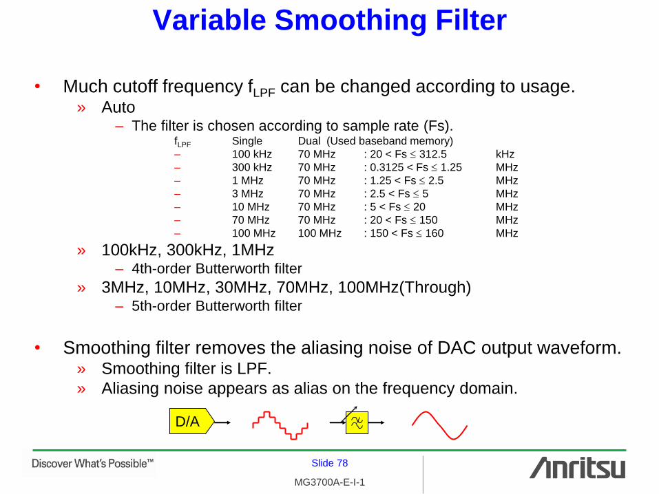
Variable Smoothing Filter
• Much cutoff frequency fLPF can be changed according to usage. » Auto
– The filter is chosen according to sample rate (Fs). fLPF Single Dual (Used baseband memory)
– 100 kHz 70 MHz : 20 < Fs 312.5 kHz
– 300 kHz 70 MHz : 0.3125 < Fs 1.25 MHz
– 1 MHz 70 MHz : 1.25 < Fs 2.5 MHz
– 3 MHz 70 MHz : 2.5 < Fs 5 MHz
– 10 MHz 70 MHz : 5 < Fs 20 MHz
– 70 MHz 70 MHz : 20 < Fs 150 MHz
– 100 MHz 100 MHz : 150 < Fs 160 MHz
» 100kHz, 300kHz, 1MHz – 4th-order Butterworth filter
» 3MHz, 10MHz, 30MHz, 70MHz, 100MHz(Through) – 5th-order Butterworth filter
• Smoothing filter removes the aliasing noise of DAC output waveform. » Smoothing filter is LPF.
» Aliasing noise appears as alias on the frequency domain.
D/A

Slide 79
MG3700A-E-I-1
Behavior of Variable Smoothing Filter
• Although the smoothing filter can be used in order to reduce the
spurious and ACLR, it affects EVM. » Trade-off of the performance
– If fLPF is set lower in order to reduce ACLR, EVM performance will degrade.
• Please select best fLPF according to signal bandwidth, in the case of
the signal generating that prioritizes ACLR performance. For example
» W-CDMA: 3 MHz
» CDMA2000: 1 MHz
» GSM/EDGE: 300 kHz
» PHS: 300 kHz

Slide 80
MG3700A-E-I-1
Tunable Baseband Amplitude
• I/Q amplitude (RMS) of DAC output level i.e. I/Q modulator input level
is tunable. » : -8 +8 dB, Resolution 0.01 dB
Q
I
22 QI
22 QI
22 QI

Slide 81
MG3700A-E-I-1
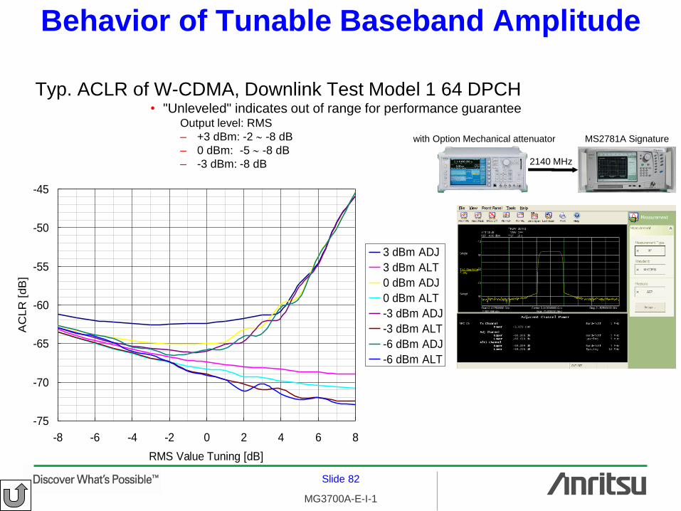
Behavior of Tunable Baseband Amplitude
• I/Q modulator input level affects EVM, origin offset, ACLR, and noise floor. » Trade-off of the performance
– If the level is gained in order to improve the performance of origin offset and noise
floor, the spectral regrowth will be caused, and then ACLR and EVM will degrade.
• Try to decrease RMS level, in the case of the signal generating that
prioritizes the adjacent channel leakage power ratio performance and
intermodulation distortion performance.
• Try to increase RMS level, in the case of the signal generating that
prioritizes the alternate channel leakage power ratio performance. » RMS level tuning changes the performance guarantee range of the output
level. – If RMS level is increased, the lower limits of output level go up the increases.
• For example 1 GHz, RMS +3 dB – Upper limits of output level: +2 dBm
– Lower limits of output level: -140 dBm + 3 dB = -137 dBm
– If RMS level is decreased, the upper limits of output level go down the decreases. • For example 1 GHz, RMS -3 dB
– Upper limits of output level: +2 dBm - 3 dB = -1 dBm
– Lower limits of output level: -140 dBm
Note: RMS level is not initialized to 0 dB, even if the signal pattern is changed.
Slide 82
MG3700A-E-I-1
Behavior of Tunable Baseband Amplitude
Typ. ACLR of W-CDMA, Downlink Test Model 1 64 DPCH • "Unleveled" indicates out of range for performance guarantee
Output level: RMS
– +3 dBm: -2 -8 dB
– 0 dBm: -5 -8 dB
– -3 dBm: -8 dB
with Option Mechanical attenuator MS2781A Signature
-75
-70
-65
-60
-55
-50
-45
-8 -6 -4 -2 0 2 4 6 8
RMS Value Tuning [dB]
AC
LR
[dB
]
3 dBm ADJ
3 dBm ALT
0 dBm ADJ
0 dBm ALT
-3 dBm ADJ
-3 dBm ALT
-6 dBm ADJ
-6 dBm ALT
2140 MHz

Slide 83
MG3700A-E-I-1
BER Analyzer
One MG3700A performs the receiver tests. » Until now a BER analyzer and an interference signal source in addition
to the wanted signal source were required. – Cost was reduced by employing LSI designed for BER analysis, and BER
analyzer was included as standard equipment.
• Clock rate » 1 k 20 MHz * Standard
» 100 120 Mbps * Option
• Data pattern » PN9, 11, 15, 20, 23, ALL0, ALL1, Alternate 01
» PN fixed pattern, Custom pattern * Option only
• Measuring bit/time (after synchronization) » 1,000 4,294,967,295 (223-1) bits
» 0.1 359,999 s (99 h 59 m 59 s), Resolution 0.1 s * Standard only
» 1 2,147,483,647 (231-1) error bits * Option only Data
Clock Wanted signal
+ Interference signal
Wanted signal
+ AWGN

Slide 84
MG3700A-E-I-1
BER Analyzer
• Real-time display » Elapsed time
» Progress rate – Automatic re-synchronization
(Auto Resync) • On: Sync Loss monitoring per 10 ms
– If 6 error bits in 64 bits occurs, Sync Loss
will be displayed and measurement will stop.
• Off: Sync Loss detection ignore
– Measure mode • Single, Continuous, Endless
» BER – Floating point (.e)
– Fixed point (. %)
» Error-bit-count
» Bit count
• Log save – Comparison with previous BER is available.
– Data for BER curve can be saved.
» Save media: HD, CF
» Maximum number of logs: 100

Slide 85
MG3700A-E-I-1
Operability
• Function keys
• Cursor/Edit keys
• Large-screen color LCD – 8.4 inch TFT
» bmp file save (HD, CF) – 640 480 pixel
• Editing menu keys » Frequency
» Output level
» Baseband
» Utility – Internal memory
management • Save/Recall the setting
status
– BERT
– System • Remote operation interface
• Network setting
• Activity log
• Configuration/Version
• Firmware upgrade
• Modulation On/Off
• RF output On/Off

Slide 86
MG3700A-E-I-1
Operability
• Panel key layout » Operability has been improved by using the rotary knob to move the
cursor, as a result of considering smooth operation flow:
[Selecting function][Moving cursor][Editing(select/input)][Enter].
• Operation guidance display » Panel operations include the parameter settings such as item selection,
data input and character input. Available key types are displayed as
guidance in pop-up window during parameter setting to enable
operation without confusion. • Example of Output level setting
Rotary knob , Step keys, ten keys, Resolution keys
• CF slot on front panel » Linking with a PC is easy in environments without a LAN by using
CompactFlash as removable media.

Slide 87
MG3700A-E-I-1
Operability
• Frequency channel setting » If assignment of the channel number is defined as frequency, frequency
will change only by setting the channel number. – Selectable: Frequency display only, Frequency and Channel display,
Channel display only
» The groups up to 19 are edited/saved in the channel table file. – Save to HD, CF
In case of secret frequency

Slide 88
MG3700A-E-I-1
Operability
• Internal memory management » All setting parameters can be saved in up to 100 files.
– File name up to 30 characters can be inputted for easy confirmation. – Save to HD, CF
or CF
Slide 89
MG3700A-E-I-1
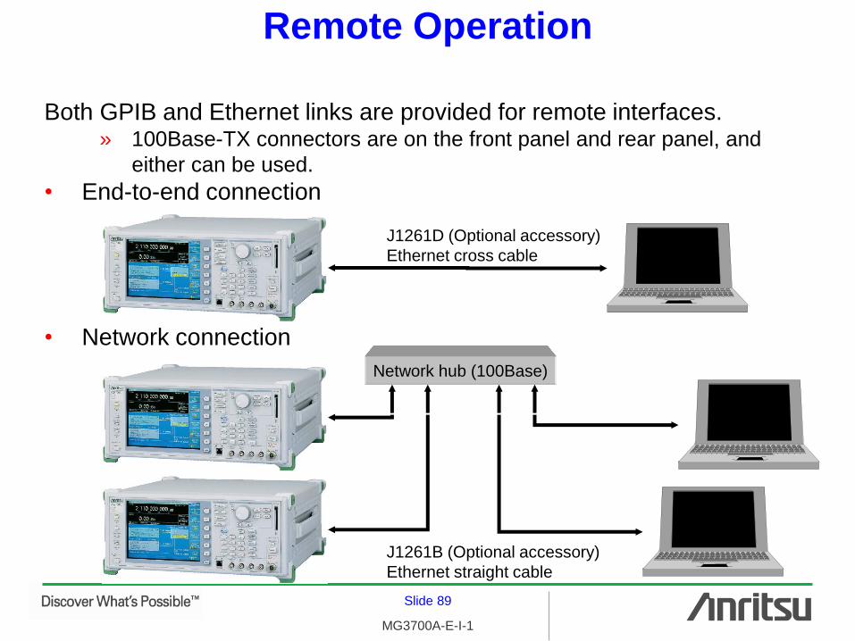
Remote Operation
Both GPIB and Ethernet links are provided for remote interfaces. » 100Base-TX connectors are on the front panel and rear panel, and
either can be used.
• End-to-end connection
J1261D (Optional accessory)
Ethernet cross cable
• Network connection
J1261B (Optional accessory)
Ethernet straight cable
Network hub (100Base)

Slide 90
MG3700A-E-I-1
Remote Operation
Network interface settings
• Ethernet » Socket Port Number: TCP/IP port number 49152 65535
• TCP/IP » Host name 30 character
» Domain name 30 character assigned from DHCP server
» DHCP – Off: IP address
Subnet mask
Default gateway
– On: • DNS server (DHCP use): On, Off
» DNS address Primary, Secondary at DHCP: Off or DNS server: Off
» Ping IP address
• FTP access key using IQproducer » User ID 8 character
» Password 8 character

Slide 91
MG3700A-E-I-1
Radiated Interference Leakage
The signal generator shield is important in minimizing the signal
generator’s radiated interference leakage, which interferes with the
receiver in low level receiver sensitivity tests. » Although MG3700A is lighter, the shielding performance of the circuitry
units has been improved.
» Shielding has been devised for the front panel CF port.
» The display has been equipped with a shielding net.
Horizontal Vertical

Slide 92
MG3700A-E-I-1
Maintainability
Shortening of downtime
• Exchange of internal HDD The signal cannot be outputted if internal HDD breaks down.
» If the HDD breaks down, the user can exchange it on-site via the rear
panel. – MTBF mean time between failures of internal HDD: 20,000 Hours
• Periodical backup of custom files is recommended using "IQproducer" of standard
accessory.
» If the MG3700A breaks down, the HDD for the failed MG3700A can be
installed in a MG3700A loaner. – Resetting is unnecessary.
» Confidential setting can be preserved. – Pull out when shipping for repair.
G0141(Optional accessory)
HDD ASSY assembly
– 2.5 inch for notebook PC
– The files at MG3700A delivery is saved.
Be careful not to damage the connection pins when inserting HDD.

Slide 93
MG3700A-E-I-1
Maintainability
Reliable usage for ATE
• Automatic check for useful life of mechanical step attenuator and
mechanical switch » Warning is released when useful life is exceeded after switching 5
million times.
• Self-check » Automatic alarm at emergence of trouble
– Output level ALC trouble
– Temperature trouble (Internal temperature > 70 C)
» Alarm log file – It can been saved to HD or CF for troubleshooting.

Slide 94
MG3700A-E-I-1
Maintainability
The users can upgrade the firmware.
• The user can visit the Anritsu "Software Download" website to
download the latest firmware and operation manuals (PDF) for free. – User registration is required to use the download service.
or HD
http://www.anritsu.com/

Slide 95
MG3700A-E-I-1
Features
• Product Outline
• Features » Instrument
Platform
» Software
• Options
• IQproducer 96
• Standard Signal Pattern Files
Optional Signal Pattern Files
127
» IQproducer and standard signal
pattern files are MG3700A
standard accessory. – IQproducer is stored in CD
together with Operation
Manuals (PDF).
– Standard signal pattern files
are saved in HDD.
HDD

Slide 96
MG3700A-E-I-1
IQproducer
• Windows software utility operating on PC » User-friendly graphical user interface (GUI)
• Creates pattern files for internal I/Q baseband generator » Sets signal parameters flexibly
– User-friendly GUIs focused on specific signal formats
» Links to EDA tools – Importable ASCII text CSV files of I/Q sample data to the signal pattern files
for MG3700A
» Creates arbitrary AWGN patterns
» Applies peak clipping and bandlimiting filter to pattern file
» Edits scenario for sequence and combination of signal patterns
• Plots simulation of CCDF, FFT spectrum, and time domain
• FTP connection to MG3700A internal HDD » FTP between internal HDD and PC
• Remote operation for signal generation » Loads the pattern files from internal HDD to baseband memory
» Selects the pattern to generate

Slide 97
MG3700A-E-I-1
Hardware Requirements
Personal computer
• OS: Windows 2000, XP
• Memory: 512 MB recommendation
• Display: 1,024 768 pixel
LAN

Slide 98
MG3700A-E-I-1
Creates Pattern Files: Sets Signal Parameters Flexibly
• Since these are recorded on CD of MG3700A standard accessories, the user can
try the functionality before purchase.
• License option » MX370101A HSDPA/HSUPA IQproducer
• Focuses on DL/UL RMC formats for HSPA/W-CDMA
» MX370102A TDMA IQproducer • Focuses on universal TDMA formats for ASK, FSK, PSK, QAM
» MX370103A CDMA2000 1xEV-DO IQproducer • Focuses on Forward/Reverse signal formats for CDMA2000 1xEV-DO (Rev.0)
» MX370104A Multi-carrier IQproducer • Focuses on multi-carrier with any signal formats and Test Model formats for
HSDPA/W-CDMA
» MX370105A Mobile WiMAX IQproducer • Focuses on OFDMA formats for IEEE802.16e
* The other datasheets and literatures show the more information.

Slide 99
MG3700A-E-I-1
Creates Pattern Files: Sets Signal Parameters Flexibly
• Since these are recorded on CD of MG3700A standard accessories, the user can
try the functionality before purchase.
• License option » MX370106A DVB-T/H IQproducer
• Focuses on OFDM broadcast for DVB-T/H
» MX370107A Fading IQproducer • Focuses on universal fading channels containing MIMO
» MX370108A LTE IQproducer • Focuses on DL/UL signal formats for 3GPP LTE
* The other datasheets and literatures show the more information.

Slide 100
MG3700A-E-I-1
Creates Pattern Files: Sets Signal Parameters Flexibly
• Non-license » Limited W-CDMA IQproducer
• Focuses on DL/UL RMC formats for W-CDMA – Limited version for parameter editing of HSDPA/HSUPA IQproducer
* The other datasheets and literatures show the more information.

Slide 101
MG3700A-E-I-1
License Key for MX3701xx IQproducer
• If MX3701xx IQproducer is purchased, CD containing the license key
file on MG3700A serial number will be provided. » The same IQproducer as standard accessory and Operation Manual
(PDF) are also contained in CD.
• In order to download the signal pattern file created using the
MX3701xx IQproducer to baseband memory, installing the license
key file per MG3700A is required. » When MX3701xx IQproducer is purchased together with MG3700A, the
license key file is already installed in MG3700A.
to MG3700A internal memory
Appear on the additional line
or CF

Slide 102
MG3700A-E-I-1
Creates Pattern Files: Links to EDA Tools
EDA tools such as "MATLAB" and "Microwave Office" can save IQ
simulation data to ASCII text CSV files. » It is made easy to compare simulation data and the measured data.
• Importable ASCII text CSV files to the signal pattern files for
MG3700A » ASCII text CSV files
– I channel data
– Q channel data
– Markers data (3 event markers and RF gate flag)
Import » Signal pattern files for MG3700A
– .wvi text file (Header file) • The configuration information of the signal patterns is saved.
– .wvd binary file (IQ sample data file) • The data of I channel, Q channel, markers is saved.

Slide 103
MG3700A-E-I-1
Convertible Files
• Importable file into MG3700A » ASCII text files
– CSV format in which data is saved to one file ASCII1 • I channel, Q channel, Event markers
– CSV format in which data is saved to two files ASCII2 • I channel Q channel
– CSV format in which data is saved to three files ASCII3 • I channel Q channel Event markers
» MS2690 digitized file MS269x Digitizer
» Signal pattern file for MS2690-20 (VSG) MS269x (to MG3700)
• Exportable signal pattern files for MG3700A into MS2690-20 (VSG) » Signal pattern files for MG3700A MG3700 (to MS269x)
– .wvi text file (Header file)
Export » Signal pattern files for MS2690-20
– .wvi text file (Header file)
Source file
Slide 104
MG3700A-E-I-1
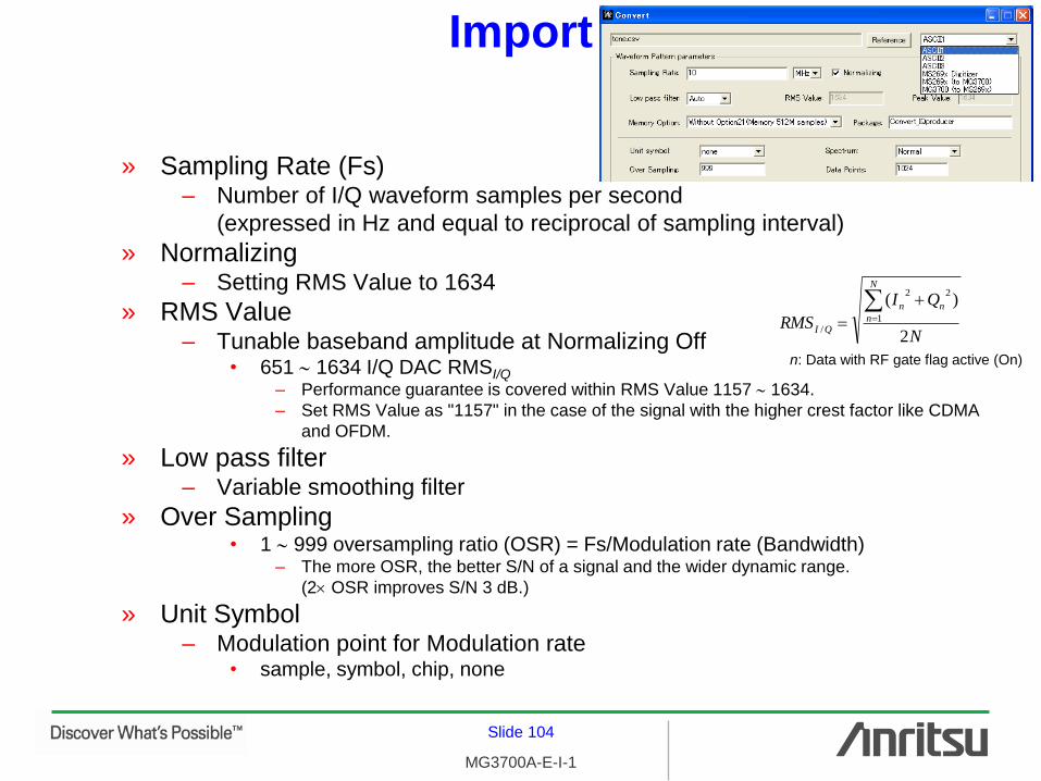
Import
» Sampling Rate (Fs) – Number of I/Q waveform samples per second
(expressed in Hz and equal to reciprocal of sampling interval)
» Normalizing – Setting RMS Value to 1634
» RMS Value – Tunable baseband amplitude at Normalizing Off
• 651 1634 I/Q DAC RMSI/Q – Performance guarantee is covered within RMS Value 1157 1634.
– Set RMS Value as "1157" in the case of the signal with the higher crest factor like CDMA
and OFDM.
» Low pass filter – Variable smoothing filter
» Over Sampling • 1 999 oversampling ratio (OSR) = Fs/Modulation rate (Bandwidth)
– The more OSR, the better S/N of a signal and the wider dynamic range.
(2 OSR improves S/N 3 dB.)
» Unit Symbol – Modulation point for Modulation rate
• sample, symbol, chip, none
N
QI
RMS
N
n
nn
QI2
)(1
22
/
n: Data with RF gate flag active (On)

Slide 105
MG3700A-E-I-1
Import
Burst Setting
– Definition of frame length in use of input frame trigger
– Saving of the baseband memory in the case of a burst signal because burst-off period doesn’t need sample data.
» Frame Length – Frame samples
– Real frame length = Frame Length + Gap Length
» Gap Length – Burst gap samples
– This period holds the final sample data including event markers and RF gate flag in
Frame Length.
Unit Symbol
Frame Length Gap Length
Real frame length
Final sample

Slide 106
MG3700A-E-I-1
Import
RF Gate – This optimizes RF gate flag to scale I/Q data within burst signal for MS2690
digitized file at MS269x Digitizer.
» RF On/Off Threshold – Threshold level for automatic detection of no signal and active/inactive
(On/Off) definition of RF gate flag • 0 100%
– 100% reference level: Peak
» Minimum RF Gate Length – Minimum consecutive samples for automatic detection of no signal and
inactive (Off) definition of RF gate flag • 0 100000 samples
22
nn QI

Slide 107
MG3700A-E-I-1
Effect of RF Gate – Blue trace
• Data with RF Gate – RMSI/Q (0 dB) is
calculated from burst I/Q
data.
– Red trace • Data without RF Gate
– RMSI/Q (0 dB) is
calculated from all I/Q
data.
Peak level
(+12.9892 dB)
RF On/Off Threshold
1% (-40 dB)
Crest Factor
12.9892 dB
RF gate flag
Minimum RF Gate Length
100 samples

Slide 108
MG3700A-E-I-1
Creates Pattern Files: Creates Arbitrary AWGN Patterns
• AWGN pattern file suitable for arbitrary wireless systems can be
created easily.
» Coupled Patten File – The configuration information of the wanted signal to mix is read.
» AWGN BW (B) / Wanted Signal BW (A) • 1, 1.5, 2, 2.5 ratio
» Sampling Rate – Sample rate (Fs) corresponding to the wanted signal to mix
» AWGN BW (B) – Calculated from Wanted Signal BW (A) and AWGN BW (B) / Wanted Signal
BW (A) – BW (B) Fs/2 at BW (B) = 0.001 20 MHz
– BW (B) Fs at BW (B) = 20.001 120 MHz

Slide 109
MG3700A-E-I-1
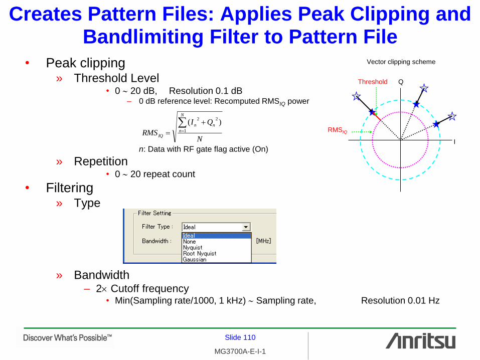
Creates Pattern Files: Applies Peak Clipping and Bandlimiting Filter to Pattern File
• Peak clipping affects spectral regrowth and EVM because of lower
PAR. – It improves the spectral regrowth, but it worsens the EVM.
• Filtering affects spectrum and EVM because of spectral shaping filter
on baseband. – It shapes up the spectrum, but it worsens the EVM.
Peak clipping Filtering Source pattern file Created pattern file
Repetition: Repeat loop
RMS power recomputing 22 QI
Slide 110
MG3700A-E-I-1
Creates Pattern Files: Applies Peak Clipping and Bandlimiting Filter to Pattern File
• Peak clipping » Threshold Level
• 0 20 dB, Resolution 0.1 dB – 0 dB reference level: Recomputed RMSIQ power
n: Data with RF gate flag active (On)
» Repetition • 0 20 repeat count
• Filtering » Type
» Bandwidth – 2 Cutoff frequency
• Min(Sampling rate/1000, 1 kHz) Sampling rate, Resolution 0.01 Hz
N
QI
RMS
N
n
nn
IQ
1
22)(
I
Q Threshold
RMSIQ
Vector clipping scheme

Slide 111
MG3700A-E-I-1
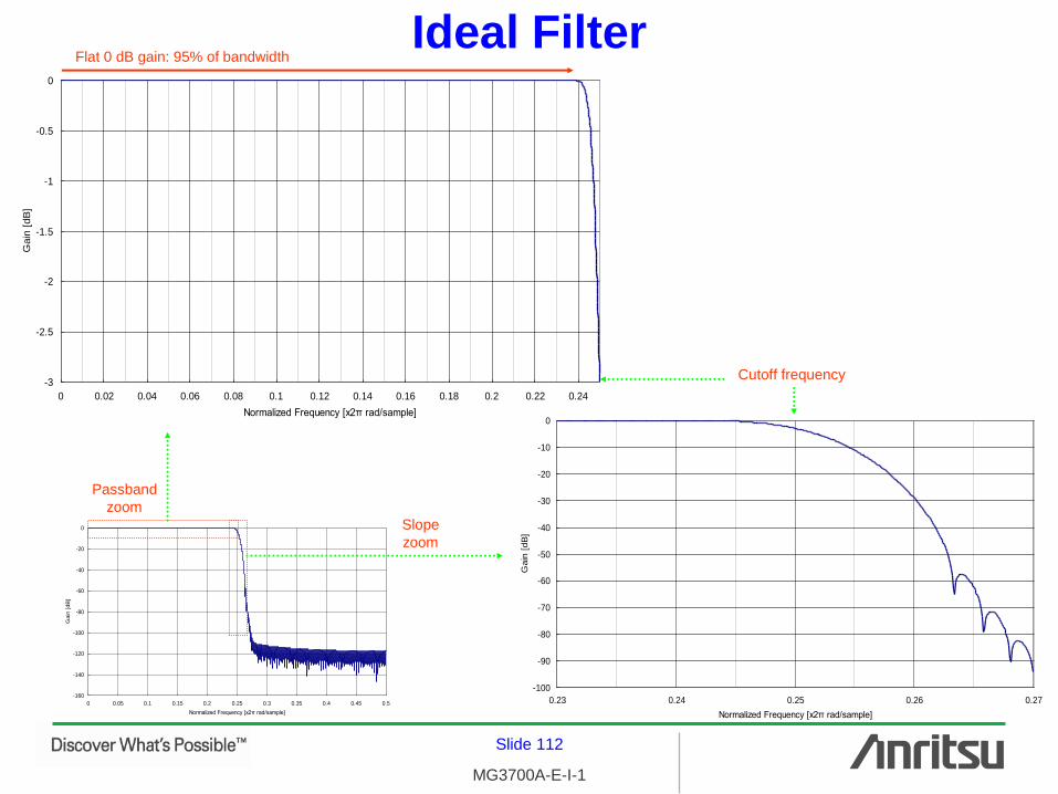
Ideal Filter
• Ideal filter is available to reduce out-of-band noises. » Example of frequency response with bandwidth/sampling rate = 1/2
-160
-140
-120
-100
-80
-60
-40
-20
0
0 0.05 0.1 0.15 0.2 0.25 0.3 0.35 0.4 0.45 0.5
Normalized Frequency [x2π rad/sample]
Gain
[dB
]
Passband Stopband
14-bit DAC S/N
= 86.04 dB
= 6.02 * 14 + 1.76
Frequency [Hz] = Normalized frequency * Sampling rate
Slide 112
MG3700A-E-I-1
Ideal Filter
-160
-140
-120
-100
-80
-60
-40
-20
0
0 0.05 0.1 0.15 0.2 0.25 0.3 0.35 0.4 0.45 0.5
Normalized Frequency [x2π rad/sample]
Gain
[dB
]
-3
-2.5
-2
-1.5
-1
-0.5
0
0 0.02 0.04 0.06 0.08 0.1 0.12 0.14 0.16 0.18 0.2 0.22 0.24
Normalized Frequency [x2π rad/sample]
Gain
[dB
]
Passband
zoom
Slope
zoom
Flat 0 dB gain: 95% of bandwidth
Cutoff frequency
-100
-90
-80
-70
-60
-50
-40
-30
-20
-10
0
0.23 0.24 0.25 0.26 0.27
Normalized Frequency [x2π rad/sample]
Gain
[dB
]

Slide 113
MG3700A-E-I-1
Effect of Peak Clipping and Filtering
» Example of OFDM signal – Blue trace
• Source data
– Red trace • Data with 10 dB clipping
and ideal filtering
Threshold

Slide 114
MG3700A-E-I-1
Creates Pattern Files: Edits Scenario for Sequence and Combination
» Combination file – .wvc text file
– The setting status is
saved.
• Sequence for protocol
emulation » Repeat Count
• 1 65,535 / (endless)
Maximum
element
200

Slide 115
MG3700A-E-I-1
Creates Pattern Files: Edits Scenario for Sequence and Combination
• Sequence for digital sweep of
output level » Level
• -80 0 dB – 0 dB reference level:
MG3700A setting RF
level
• Combination » Add Pattern
– Pattern for baseband
memory B
f
Opening of the existing combination file
t

Slide 116
MG3700A-E-I-1
Plots Simulation of CCDF, FFT Spectrum, Time Domain
• CCDF Complementary Cumulative Distribution Function curve » Plots the cumulative distribution of instantaneous power/mean power
– If PAR Peak to Average power Ratio or Crest Factor of the signal is higher, the
nonlinear elements will cause the spectral regrowth, and will affect ACLR.
• FFT Fast Fourier Transform Spectrum » Plots the frequency spectrum
– Converting time-based signal into frequency domain
• Time domain » Plots the I/Q waveform, markers activity and power trace into time
domain – Available to reconfigure markers data

Slide 117
MG3700A-E-I-1
CCDF
Plots the signal patterns up to 8
Plots the gaussian trace
Adds or deletes CCDF curve
Plots in conjunction with IQproducer
under System menu
Operation of the mouse dragging on graph area
- Cursor motion
- Zoom of the scope of selection

Slide 118
MG3700A-E-I-1
FFT
Select lower value than Data Length
Adds or deletes spectrum
Range of the sample data to compute
Plots in conjunction with IQproducer
under System menu
Operation of the mouse dragging on graph area
- Cursor motion
- Zoom of the scope of selection
Plots the signal patterns up to 4
on same sampling rate

Slide 119
MG3700A-E-I-1
Time Domain
Plots the signal patterns up to 4
Adds or deletes trace
Trace range
I/Q waveform
Power
Operation of the mouse dragging on graph area
- Cursor motion
- Zoom of the scope of selection
Plots in conjunction with IQproducer under System menu
Reconfigurable markers data

Slide 120
MG3700A-E-I-1
Marker Edit
» Start Point
– Offset inactive samples
» Width – Pulse width samples
» Period – Pulse period samples
New pattern file
t
Markers data Active (On)
Inactive (Off)
Start Point Period Period
Width Width Width
I/Q data

Slide 121
MG3700A-E-I-1
FTP Connection to Internal HDD
• Transfer & Setting Panel » Files transfer to multi-MG3700A internal HDD, and backup of HD
• Signal pattern files
• Parameter files
• Channel table files
• BER log files
• Alarm log files
• Screen copy files
• Firmware updated files
» Remote operation for signal generation
• Transfer & Setting Wizard » Step-by-step operation for a pattern file transfer and generating
– Step 1: FTP connection to one MG3700A
– Step 2: Selection of a package for a pattern file to transfer to MG3700A
internal HDD
– Step 3: Remote operation for selection and generation of the pattern file

Slide 122
MG3700A-E-I-1
• Transfer & Setting Panel
» Server based network
connection – Enter the host name of
MG3700A. • Enter the IP address of
MG3700A, when the domain
name is not defined.
» End-to-end connection – Enter the IP address of
MG3700A. • PC has different IP address
with MG3700A.
FTP Connection
• Transfer & Setting Wizard

Slide 123
MG3700A-E-I-1
FTP Connection Connect
Disconnect
Toolbar
Folder
address
PC side SG(MG3700A) side
Saved
package (folder)
MG3700A status bar
Free space / Full capacity
Internal HDD, Baseband memory

Slide 124
MG3700A-E-I-1
Transfer, Remote Operation
PC to SG
SG to PC
PC to All SG
Under
generating
A, B: for signal pattern files(.wvi)
C: for combination files (.wvc) Copy Download to
baseband memory
Delete from
baseband memory
Generate the selected pattern
FTP log

Slide 125
MG3700A-E-I-1
Transfer Wizard
Select the package to copy
PC to SG
Select one pattern file to copy
Download to baseband memory Generate the selected
Pattern file

Slide 126
MG3700A-E-I-1
Release Version Check
• The user can visit the Anritsu "Software Download" website to
download the latest IQproducer and operation manuals (PDF) for
free. – User registration is required to use the download service.
http://www.anritsu.com/

Slide 127
MG3700A-E-I-1
Standard Signal Pattern Files
• Standard signal pattern files are the signal formats based on the
receiver/transmitter test specifications for base stations and terminals
of the major wireless systems.
• Easy operation just selects the signal pattern saved to high-capacity
HDD, without setting the troublesome signal parameters for a
wireless system.
• Useful for production and installation/maintenance application
Lineup • WLAN (IEEE802.11a/b/g)
• W-CDMA
• GSM/EDGE
• CDMA2000 1xEV-DO (Rev.0)
• CDMA2000 1X
• PHS
• PDC
• Bluetooth
• GPS
• Digital Broadcast (BS, CS, CATV, ISDB-T)
* The other datasheets show the more information.

Slide 128
MG3700A-E-I-1
WLAN Outline
• AP/STA transmitter test
• AP/STA receiver test » IEEE802.11a/g OFDM 6 54 Mbps
– 40 MS/s, 16.6 MHz bandwidth
» IEEE802.11b/g DSSS 1, 2 Mbps
CCK 5.5, 11 Mbps – 44 MS/s, 22 MHz bandwidth
» IEEE802.11g (Optional) DSSS-OFDM 6 54 Mbps – 40 MS/s, 16.6 MHz bandwidth

Slide 129
MG3700A-E-I-1
• BS transmitter test » Test Model 1 5
» Multi-carrier • 4 Test Model 1 64DPCH
• 3 Test Model 1 64DPCH
• 2 Test Model 1 64DPCH
– Scrambling Code 0H, 10H
(+5 MHz), 20H(+10 MHz), 30H
(+15 MHz)
– Oversampling 4 3.84 Mcps = 15.36 MS/s
W-CDMA Outline
CF
CF
CF CF CF

Slide 130
MG3700A-E-I-1
W-CDMA Outline
• BS receiver test » UL RMC 12.2 384 kbps
» UL AMR
» UL ISDN
» UL Packet 64 kbps – Scrambling Code 0H
– Oversampling 3 3.84 Mcps = 11.52 MS/s
– UL RMC 12.2 kbps also has Oversampling 4 3.84 Mcps = 15.36 MS/s.
» UL Interferer – Scrambling Code 1H
– Oversampling 3 3.84 Mcps = 11.52 MS/s
Maximum frequency offset (f): 34.944 MHz
– Oversampling 4 3.84 Mcps = 15.36 MS/s
Maximum frequency offset (f): 47.232 MHz

Slide 131
MG3700A-E-I-1
W-CDMA Outline
• UE transmitter test » UL RMC 12.2 kbps
– Scrambling Code 0H – Oversampling 3 3.84 Mcps = 11.52 MS/s
• UE receiver test » DL RMC 12.2 384 kbps *
» DL AMR *
» DL ISDN *
» DL Packet 384 kbps * – Scrambling Code 80H
» DL Interferer – Scrambling Code 0H
– Oversampling 4 3.84 Mcps = 15.36 MS/s
*: To mix P-CCPCH (4096 frames) with full SFN 11 bit count (0 2047)

Slide 132
MG3700A-E-I-1
GSM/EDGE Outline
• BS/MS transmitter test » No timeslot format PN9 (And also for interference signal)
» No burst format TN0
» No channel coding NB Normal burst TN0, TN0 7 (All slots)
• BS/MS receiver test » TCH/FS Full rate Speech TCH TN0
» CS-1, CS-4 GPRS PDTCH TN0
» MCS-1, MCS-5 EGPRS PDTCH TN0
» MCS-9 EGPRS PDTCH TN0, TN0 3
– Oversampling 8 270.833 ksps = 2,166.7 kS/s
*TN: Timeslot Number
GMSK 8PSK
8PSK GMSK

Slide 133
MG3700A-E-I-1
CDMA2000 1xEV-DO Outline
• AN/AT transmitter test
• AN/AT receiver test » Forward 38.4 2,457.6 kbps (Active slot), Idle slot
» Reverse 9.6 153.6 kbps – Long Code Mask (42 bits)
• MI: 3FF00000000H
• MQ: 3FF00000001H
– Oversampling 4 1.2288 Mcps = 4.9152 MS/s

Slide 134
MG3700A-E-I-1
CDMA2000 1X Outline
• BS/MS transmitter test
• BS receiver test » Forward RC 1/2 (6 FCH 19.2 ksps)
RC 3/4/5 (6 FCH 38.4 ksps) – No coding
» Reverse RC 1 FCH 9.6 kbps
RC 2 FCH 14.4 kbps
RC 3 PICH + FCH 9.6 kbps
PICH + FCH 9.6 kbps + SCH 9.6 kbps
PICH + DCCH 9.6 kbps
RC 4 PICH + FCH 14.4 kbps – Long Code Mask (42 bits) 00000000000H
– Oversampling 4 1.2288 Mcps = 4.9152 MS/s

Slide 135
MG3700A-E-I-1
PHS, PDC Outline
PHS
• CS/PS transmitter test » No /4DQPSK slot format PN9, All’0’
• CS/PS receiver test » /4DQPSK TCH Slot 1
» No /4DQPSK slot format PN15 – Oversampling 8 192 ksps = 1,536 kS/s
PDC
• BS/MS transmitter test » No slot format PN9
• BS/MS receiver test » TCH full rate Slot 0
» TCH half rate Slot 0
» PDC-P Slot 0, Slot 0/1 *Downlink, Slot 0/1/2 *Downlink
» No slot format PN15 – Oversampling 8 21 ksps = 168 kS/s

Slide 136
MG3700A-E-I-1
Bluetooth Outline
• Transmitter test
• Receiver test » No packet format PN9, PN15 GFSK, /4DQPSK, 8DPSK
» DH1, DH3, DH5 Basic Rate GFSK Payload
» 2-DH1, 2-DH3, 2-DH5 EDR /4DQPSK Payload
» 3-DH1, 3-DH3, 3-DH5 EDR 8DPSK Payload
» POLL System packet for functionality test
» 2/3-DH1/3/5 dirty signals EDR /4DQPSK, 8DPSK Payload
– Oversampling 12 1 Msps = 12 MS/s
Transmission
Packets
Carrier
Offset
Frequency
Symbol
Timing
Error
1 20 Packets 0 kHz 0 ppm
2 20 Packets +65 kHz +20 ppm
3 20 Packets -65 kHz -20 ppm 1 slot t
DH1
2-DH1
3-DH1
POLL
DH3
2-DH3
3-DH3
DH5
2-DH5
3-DH5
DH3_3SlotOff
2-DH3_3SlotOff
3-DH3_3SlotOff
DH5_5SlotOff
2-DH5_5SlotOff
3-DH5_5SlotOff
Burst slots map

Slide 137
MG3700A-E-I-1
GPS Outline
• GPS receiver test » No subframe format PN9
» Subframe for parity detection PARITY – Subframe ID 1
» Subframe for sensitivity test TLM – Subframe ID 1
» Frame for sensitivity test TLM_PARITY – Subframe ID 1 5
– Oversampling 4 1.023 Mcps = 4.092 MS/s
Trigger delay setting ability 244 ns 1/4.092 us
• Satellite ID 1
240 bits

Slide 138
MG3700A-E-I-1
GPS Outline
• A-GPS receiver test » Subframe for time calibration SYNC_ADJ
It is used use when synchronizing with PP2S.
– Subframe ID 1
– Oversampling 100 1.023 Mcps = 102.3 MS/s
Trigger delay setting ability 9.8 ns 1/102.3 us
• Satellite ID 1
Combination file
Nested signal pattern files
240 bits

Slide 139
MG3700A-E-I-1
GPS Outline 300 bits 6 s

Slide 140
MG3700A-E-I-1
Digital Broadcast Outline
• Transmitter test » Digital BS (ISDB-S) QPSK Roll-off 0.35
– 144.3 MS/s, 34.5 MHz bandwidth
» Digital CS QPSK Roll-off 0.35 – 147.672 MS/s, 27 MHz bandwidth
» CATV (ITU-T J83 Annex C) 64QAM Roll-off 0.13 – 42.192 MS/s, 6 MHz bandwidth
» ISDB-T TSPA(13 segments) 64QAM
TSPA(1 segment) QPSK + TSPB(12 segments) 64QAM • Mode 3, GI 1/8
– 16.253968 254 MS/s, 5.572 MHz bandwidth

Slide 141
MG3700A-E-I-1
Digital Broadcast Outline
• ISDB-T receiver test » TSPA(1 segment) QPSK 2/3 + TSPB(12 segments) 64QAM 3/4 or 7/8
– TSPA/TSPB Payload: Video + Audio
– 40 frames length (9.3 s)
» TSPA(1 segment) QPSK 2/3 or 1/2, 16QAM 1/2
+ TSPB(12 segments) 64QAM 3/4 or 7/8 – TSPA/TSPB Payload: PN23 initialized at start of 4 frames
– 4 frames length (0.9 s) • Mode 3, GI 1/8
– 16.253968 254 MS/s, 5.572 MHz bandwidth
f
Segment 11 9 7 5 3 1 0 2 4 6 8 10 12
HDTV (High Definition TV) or SDTV (Standard Definition TV)
Handheld TV
64QAM 64QAM 64QAM 64QAM 64QAM 64QAM 64QAM 64QAM 64QAM 64QAM 64QAM 64QAM
QPSK
or
16QAM
6 MHz
TSPB
TSPA

Slide 142
MG3700A-E-I-1
Digital Broadcast Outline
• ISDB-Tsb receiver test » TSPA(1 segment) QPSK 1/2 + TSPB(2 segments) QPSK 1/2
– TSPA/TSPB Payload: Video + Audio
– 68 frames length (15.7 s)
» TSPA(1 segment) QPSK 1/2 or 2/3, 16QAM 1/2
+ TSPB(2 segments) 16QAM 1/2 – TSPA/TSPB Payload: PN23 initialized at start of 4 frames
– 4 frames length (0.9 s) • Mode 3, GI 1/8
– 8.126984 17 MS/s, 3.429563 49 MHz bandwidth
f
Segment 1 2 3 4 5 6 7 8
1 segment receiving
QPSK
or
16QAM
QPSK
or
16QAM
QPSK
or
16QAM
QPSK
or
16QAM
QPSK
or
16QAM
QPSK
or
16QAM
QPSK
or
16QAM
QPSK
or
16QAM
4 MHz
3 segments receiving
TSPB
TSPA TSPA TSPA TSPA TSPA TSPA

Slide 143
MG3700A-E-I-1
AWGN Outline
• For W-CDMA » 1.5 3.84 MHz = 5.76 MHz bandwidth
» 2 3.84 MHz = 7.68 MHz bandwidth – Oversampling 3 3.84 Mcps = 11.52 MS/s
• For CDMA2000 » 1.5 1.2288 MHz = 1.8432 MHz bandwidth
» 2 1.2288 MHz = 2.4576 MHz bandwidth – Oversampling 4 1.2288 Mcps = 4.9152 MS/s

Slide 144
MG3700A-E-I-1
Optional Signal Pattern Files
• Optional signal pattern files are the signal formats based on the
receiver/transmitter test specifications for base stations and terminals
of specific wireless systems.
• License option » MX370001A TD-SCDMA waveform pattern
– DL/UL RMC of 3GPP TS 25.142/102 1.28 Mcps TDD option • DVD stored together with Operation Manual (PDF) is provided.
* The other datasheets show the more information.

Slide 145
MG3700A-E-I-1
License Key for Optional Signal Pattern Files
• If optional signal pattern files are purchased, CD (DVD) containing
the license key file on MG3700A serial number will be provided.
• In order to download the optional signal pattern files to baseband
memory, installing the license key file per MG3700A is required. » When optional signal pattern files are purchased together with
MG3700A, the license key file is already installed in MG3700A.
to MG3700A internal memory
or CF
Appear on the additional line

Slide 146
MG3700A-E-I-1
TD-SCDMA Outline
• BS transmitter test » DL 1 DPCH, 8 DPCH, 10 DPCH, P-CCPCH
– Scrambling Code 0H
• BS receiver test/ UE transmitter test » UL RMC 12.2 384 kbps
– Scrambling Code 0H
• UE receiver test » DL RMC 12.2 384 kbps
– Scrambling Code 0H
– Oversampling 4 1.28 Mcps = 5.12 MS/s

Slide 147
MG3700A-E-I-1
Updated Signal Pattern Files
• The user can visit the Anritsu "Software Download" website to
download the updated latest pattern files and operation manuals
(PDF) for free. – User registration is required to use the download service.
– The pattern files are deleted two months after an announcement due to bulk files.
• All the latest pattern files are provided
by DVD for a fee. • Z0777 (optional accessory)
Standard waveform pattern upgrade kit
http://www.anritsu.com/

Slide 148
MG3700A-E-I-1
Option
• Product Outline
• Features
• Options
• MG3700A-002 (102) 149 » Mechanical Attenuator
MG3700A- (103) » Electronic Attenuator
• MG3700A-011 (111) 151 » Upper Frequency 6 GHz
• MG3700A-021 (121) 152 » ARB Memory Upgrade
512 Msample/channel
• MG3700A-031 (131) 153 » High-speed BER Test function
• MG3700A-0: Initial order
• MG3700A-1: Retrofit order
• Key optional accessories list 160

Slide 149
MG3700A-E-I-1
MG3700A-002 Mechanical Attenuator
• In order to change the RF output level widely, the step attenuator
controls the output level.
• There are two types of step attenuators. An electronic attenuator is
provided as standard. Please determine needs according to usage,
since there are trade-off relationships regarding advantages.
» Electronic step attenuator Standard
– Switches the attenuation elements using a semiconductor switch
– 5 dB step, 135 dB range
– Advantage: high-speed, long life, no wear
Better for ATE
» Mechanical step attenuator Option – Switches the contacts of a multi-fixed attenuator of different values and
through paths using a mechanical switch
– 2 dB step, 142 dB range, Switching useful life 5 million times
– Advantage: low loss, no variation of temperature
Better for high power output, high C/N, field site use

Slide 150
MG3700A-E-I-1
Different Attenuator Specifications
Electronic attenuator Mechanical attenuator MG3681A Mechanical
attenuator for reference
Frequency Switching time * Frequency switching = Normal:
15 ms (3 GHz non-cross, f < 1 GHz)
20 ms (3 GHz non-cross, f 1 GHz)
40 ms (3 GHz cross)
* Frequency switching = Fast:
10 ms (3 GHz non-cross)
40 ms (3 GHz cross)
80 ms (3 GHz non-cross)
100 ms (3 GHz cross)
20 ms
Output level Settable range -140 ~ +13 dBm -140 ~ +19 dBm -143 ~ +17 dBm
Accuracy
CW, 23 5 C CW, 23 5 C CW (0 ~ 50 C)
Switching time 10 ms ( 25 MHz)
15 ms (< 25 MHz)
80 ms 50 ms
VSWR 1.3 ( 3 GHz)
1.55 (> 3 GHz)
1.25 ( 3 GHz)
1.35 (> 3 GHz)
Vector mod. W-CDMA Test Model 1 64DPCH
I/Q mod.
ACLR 5 MHz Offset -61 dBc/3.84 MHz
-63 dBc/3.84 MHz typ.
-62 dBc/3.84 MHz
-64 dBc/3.84 MHz typ.
-66 dBc/3.84 MHz typ.
ACLR 10 MHz Offset -66 dBc/3.84 MHz typ. -67 dBc/3.84 MHz typ. -67 dBc/3.84 MHz typ.
Slide 151
MG3700A-E-I-1
MG3700A-011 Upper Frequency 6 GHz
• Upper frequency reaches 6 GHz by mounting RF unit for
3 GHz < frequency 6 GHz Standard Option
» Frequency range 250 k 3 GHz 250 k 6 GHz
• The frequency switch between RF unit for frequency 3 GHz and RF
unit for 3 GHz < frequency 6 GHz is made using a mechanical
switch. » Switching useful life 5 million times

Slide 152
MG3700A-E-I-1
MG3700A-021 ARB Memory Upgrade 512 Msample/channel
• Upgradable baseband memory capacity » Doubles the I/Q sample data sequence length
» Increases the loadable number of signal patterns – Although the data loading speed from HDD to baseband memory is 14
MB/s, the change of the signal pattern within the memory is the instant.
Better for W-CDMA and broadcast receiver test
Standard Option
» Memory capacity 2 128 M 2 256 M sample/channel
(1 GB) (2 GB)

Slide 153
MG3700A-E-I-1
MG3700A-031 High-speed BER Test Function
• Upgradable features by mounting PCB for Faster BER analyzer
Standard Option
Data rate 1 k 20 Mbps 100 120 Mbps
Data pattern PN9, 11, 15, 20, 23, ALL0, ALL1, Alternate 01
PN fixed pattern, Custom pattern
Measuring bit * after synchronization 1,000 4,294,967,295 (223-1)
Measuring time * after synchronization 0.1 359,999 s (99 h 59 m 59 s)
Resolution 0.1 s
Measuring error bit * after synchronization 1 2,147,483,647 (231-1)
Automatic re-synchronization (Auto Resync) On: Sync Loss monitoring per 10 ms
Sync Loss behavior Measurement stop (Sync Loss error) Re-synchronization (Sync Loss count)
Sync Loss threshold 6 error bits
64 bits
1 Error bits for half of bits
500 or 5,000 or 50,000 bits
Off: Sync Loss detection ignore
Input level TTL 0 5 V
Input threshold 0.8 2.4 V for TTL 0.2 3 V Resolution 0.05 V
Input impedance High impedance High impedance, 50
Input timing adjustment Data, Enable: -1 +15 clock

Slide 154
MG3700A-E-I-1
Advanced BER Analyzer
Auto Resync
described later
PN fixed pattern
Custom pattern
described later

Slide 155
MG3700A-E-I-1
PN Fixed Pattern
• The PN in PN sequence stands for pseudo noise, which is just
another name for PRBS. » PRBS: Pseudorandom binary (bit) sequence
• Pseudorandom sequences are generated using a binary shift
register. » PN(n) sequences are 2n-1 bits period
– PN9: 511 bits period
– PN11: 2,047 bits period
– PN15: 32,767 bits period
– PN20: 1,048,575 bits period
– PN23: 8,388,607 bits period
The signal pattern file created with these bits periods for BER test will
be a large file.
In order to reduce the pattern file size

Slide 156
MG3700A-E-I-1
PN Fixed Pattern
• PN fixed pattern is a data pattern initialized at the start of the frame
etc.

Slide 157
MG3700A-E-I-1
Custom Pattern
• Arbitrary data patterns can be defined on PC. » 8 1,024 bits period
Text file
00000000
11111111
01010101
00001111 Ethernet

Slide 158
MG3700A-E-I-1
Automatic Re-synchronization (Auto Resync)
• On » The error bits more than
threshold occurred after
synchronization is judged to
Sync Loss, and then the data
pattern is re-synchronized.
• Off » Sync Loss is not detected.
Recommended setting
Threshold of other models
– MP1201C
200/512
– MD6420A default
200/512
– MT8820A (W-CDMA)
23/64
Auto Resync On Auto Resync Off
Error rate Threshold 50/500 Threshold 200/500
0.3 % Not recommended Optimum Applicable
< 0.3 % Optimum Applicable Applicable
Start of BER measurement
Synchronization
(Sync Loss?)
Count (10 ms)
Stop?
Stop of count
Measure Mode?
End
Yes
No
Yes
No
Single
Endless
Continuous
Display
Synchronizing
Measuring
Stop
Slide 159
MG3700A-E-I-1
Synchronization
Standard
• Conditions » Error-free bits detection
• Probability » Probability that Error-free
(50 + n) bits occur
Option
» Probability that Error-free
(2 n) bits occur
Error rate PN9 PN15 PN23 Error rate PN9 PN15 PN23
10 % 0.22 % 0.11 % 0.046 % 10 % 15 % 4.2 % 0.79 %
3 % 17.1 % 13.8 % 10.8 % 3 % 57.8 % 40.1 % 24.6 %
1 % 55.8 % 52 % 48 % 1 % 83.5 % 74 % 63 %
0.1 % 94.4 % 93.7 % 93 % 0.1 % 98.2 % 97 % 95.5 %
PN(n) 50 + n bits PN(n) 2 n bits
ALL0, ALL1, Alternate 01 48 bits ALL0, ALL1, Alternate 01 10 bits
PN fixed pattern 2 n bits >> Last bit >> First n bits
Custom pattern 8 bits customer-defined
In PN(n) sequence with random error bits

Slide 160
MG3700A-E-I-1
Key Optional Accessories List
– Various operation manuals
(booklet) • PDF files are stored in CDs
for MG3700A standard
accessories and option
software.
– J1277 IQ output adapter • D-Sub/BNC
– G0141 HDD ASSY • for internal HDD exchange
– J1261B Ethernet cable
(shield type) • Straight, 3 m
– J1261D Ethernet cable
(shield type) • Cross, 3 m
– B0329C Front cover
– B0331C Front panel handle
kit
– B0333C Rack mount kit
– MA1612A Four-port junction
pad • 5 M 3 GHz
– MP752A Termination • DC 12.4 GHz, 50
– MA2512A Band Pass Filter • 1.92 2.17 GHz

• United StatesAnritsu Company1155 East Collins Blvd., Suite 100, Richardson, TX 75081, U.S.A.Toll Free: 1-800-267-4878Phone: +1-972-644-1777Fax: +1-972-671-1877
• CanadaAnritsu Electronics Ltd.700 Silver Seven Road, Suite 120, Kanata, Ontario K2V 1C3, CanadaPhone: +1-613-591-2003 Fax: +1-613-591-1006
• Brazil Anritsu Eletrônica Ltda.Praça Amadeu Amaral, 27 - 1 Andar01327-010 - Bela Vista - São Paulo - SP - BrazilPhone: +55-11-3283-2511Fax: +55-11-3288-6940
• MexicoAnritsu Company, S.A. de C.V.Av. Ejército Nacional No. 579 Piso 9, Col. Granada11520 México, D.F., MéxicoPhone: +52-55-1101-2370Fax: +52-55-5254-3147
• United KingdomAnritsu EMEA Ltd.200 Capability Green, Luton, Bedfordshire, LU1 3LU, U.K.Phone: +44-1582-433200 Fax: +44-1582-731303
• FranceAnritsu S.A.12 avenue du Québec, Bâtiment Iris 1- Silic 612,91140 VILLEBON SUR YVETTE, FrancePhone: +33-1-60-92-15-50Fax: +33-1-64-46-10-65
• GermanyAnritsu GmbHNemetschek Haus, Konrad-Zuse-Platz 1 81829 München, Germany Phone: +49-89-442308-0 Fax: +49-89-442308-55
• ItalyAnritsu S.r.l.Via Elio Vittorini 129, 00144 Roma, ItalyPhone: +39-6-509-9711 Fax: +39-6-502-2425
• SwedenAnritsu ABBorgarfjordsgatan 13A, 164 40 KISTA, SwedenPhone: +46-8-534-707-00 Fax: +46-8-534-707-30
• FinlandAnritsu ABTeknobulevardi 3-5, FI-01530 VANTAA, FinlandPhone: +358-20-741-8100Fax: +358-20-741-8111
• DenmarkAnritsu A/S (Service Assurance)Anritsu AB (Test & Measurement)Kay Fiskers Plads 9, 2300 Copenhagen S, DenmarkPhone: +45-7211-2200Fax: +45-7211-2210
• RussiaAnritsu EMEA Ltd. Representation Office in RussiaTverskaya str. 16/2, bld. 1, 7th floor.Russia, 125009, MoscowPhone: +7-495-363-1694Fax: +7-495-935-8962
• United Arab EmiratesAnritsu EMEA Ltd.Dubai Liaison OfficeP O Box 500413 - Dubai Internet CityAl Thuraya Building, Tower 1, Suit 701, 7th FloorDubai, United Arab EmiratesPhone: +971-4-3670352Fax: +971-4-3688460
• IndiaAnritsu India Private Limited2nd & 3rd Floor, #837/1, Binnamangla 1st Stage, Indiranagar, 100ft Road, Bangalore - 560038, IndiaPhone: +91-80-4058-1300Fax: +91-80-4058-1301
• SingaporeAnritsu Pte. Ltd.60 Alexandra Terrace, #02-08, The Comtech (Lobby A)Singapore 118502Phone: +65-6282-2400Fax: +65-6282-2533
• P.R. China (Shanghai)Anritsu (China) Co., Ltd.Room 1715, Tower A CITY CENTER of Shanghai, No.100 Zunyi Road, Chang Ning District, Shanghai 200051, P.R. ChinaPhone: +86-21-6237-0898Fax: +86-21-6237-0899
• P.R. China (Hong Kong)Anritsu Company Ltd.Unit 1006-7, 10/F., Greenfield Tower, Concordia Plaza,No. 1 Science Museum Road, Tsim Sha Tsui East, Kowloon, Hong Kong, P.R. ChinaPhone: +852-2301-4980Fax: +852-2301-3545
• JapanAnritsu Corporation8-5, Tamura-cho, Atsugi-shi, Kanagawa, 243-0016 JapanPhone: +81-46-296-1221Fax: +81-46-296-1238
• KoreaAnritsu Corporation, Ltd.502, 5FL H-Square N B/D, 681Sampyeong-dong, Bundang-gu, Seongnam-si, Gyeonggi-do, 463-400 KoreaPhone: +82-31-696-7750Fax: +82-31-696-7751
• AustraliaAnritsu Pty. Ltd.Unit 21/270 Ferntree Gully Road, Notting Hill, Victoria 3168, AustraliaPhone: +61-3-9558-8177Fax: +61-3-9558-8255
• TaiwanAnritsu Company Inc.7F, No. 316, Sec. 1, NeiHu Rd., Taipei 114, TaiwanPhone: +886-2-8751-1816Fax: +886-2-8751-1817
Specifications are subject to change without notice.
1209
Printed on Recycled Paper
Please Contact:
No. MG3700A-E-I-1-(11.00) Printed in Japan 2012-11 MG