product overview - mini-circuits
TRANSCRIPT

Page 1 of 10Mini-Circuits®
www.minicircuits.com P.O. Box 35166, Brooklyn, NY 11235-0003 (718) 934-4500 [email protected]
SPI-SP8T-6G
Key Features
SPI RF SP8T Switch50Ω 1 to 6000 MHz
Case Style: PM2656
Feature Advantages
Daisy chain SPI control Allows connecting up to 50 units in series to a single power supply and 3 wire SPI control.
RF SP8T absorptive switch Wideband (1 to 6000 MHz) with high isolation (80 dB typ.), and high power rating (+27 dBm through path).
High Linearity (IP3 +50 dBm typ.) Results in little or negligible inter-modulation generation, meeting requirements for digital communications signals
Solid state switch Provides high speed (6 µs typ) switching with no wear on the switch as with electro-mechanical designs
DC Blocking No need for external DC blocking circuitry
SMP connectors Snap on RF connectors allow quick assembly and disassembly and the small size of SMP connectors makes tighter assemblies possible
Product OverviewMini-Circuits’ SPI-SP8T-6G is a low cost, high speed solid state RF SP8T absorptive switch, with control and power via a Hirose DF11 connector. The model contains an electronic, high speed (6 µs typ switching time), high linearity (IP3 50 dBm typ), SP8T switch. The RF switch is operated using a 3-wire SPI interface compatible with TTL and LVTTL voltages and allows connecting up to 50 units in series to the same control line in a ‘Daisy Chain’ configuration. The RF switch operates over a wide frequency band from 1 to 6000 MHz with high isolation (80 dB typical) making the switch perfectly suitable for a wide variety of RF applications.
The SPI-SP8T-6G is constructed in a compact, rugged metal case (3.68” x 3.27” x 0.40”) with 9 SMP(M) connectors (COM, and J1 to J8), and two Hirose DF11 connectors providing SPI control and power, one for input and one for output when connecting multiple units in series.
The Big Deal• Daisy Chain SPI Control• High Isolation (80 dB typ)• High speed switching (6 µs typ)• High power handling (+27 dBm max)• SMP snap-on RF connectors
Solid state
Generic photo used for illustration purposes only
Page 2 of 10Mini-Circuits®
www.minicircuits.com P.O. Box 35166, Brooklyn, NY 11235-0003 (718) 934-4500 [email protected]
Features• High speed switching (6 µs typ)• 1 to 6000 MHz SP8T absorptive RF switch • High power handling, +27 dBm• High linearity (IP3 +50 dBm)• High isolation (80 dB typ)• SPI control• Daisy-chain up to 50 switches to control through a
single interface (see pages 4-5)• Easy installation and operation
Rev. AM176996EDR-11677SPI-SP8T-6GRAV200427
50Ω 1 to 6000 MHzSPI RF SP8T Switch SPI-SP8T-6G
RoHS CompliantSee our web site for RoHS Compliance methodologies and qualifications
Case Style: PM2656
Applications• R&D • Automated Test equipment• Controlling RF signal paths
Solid state
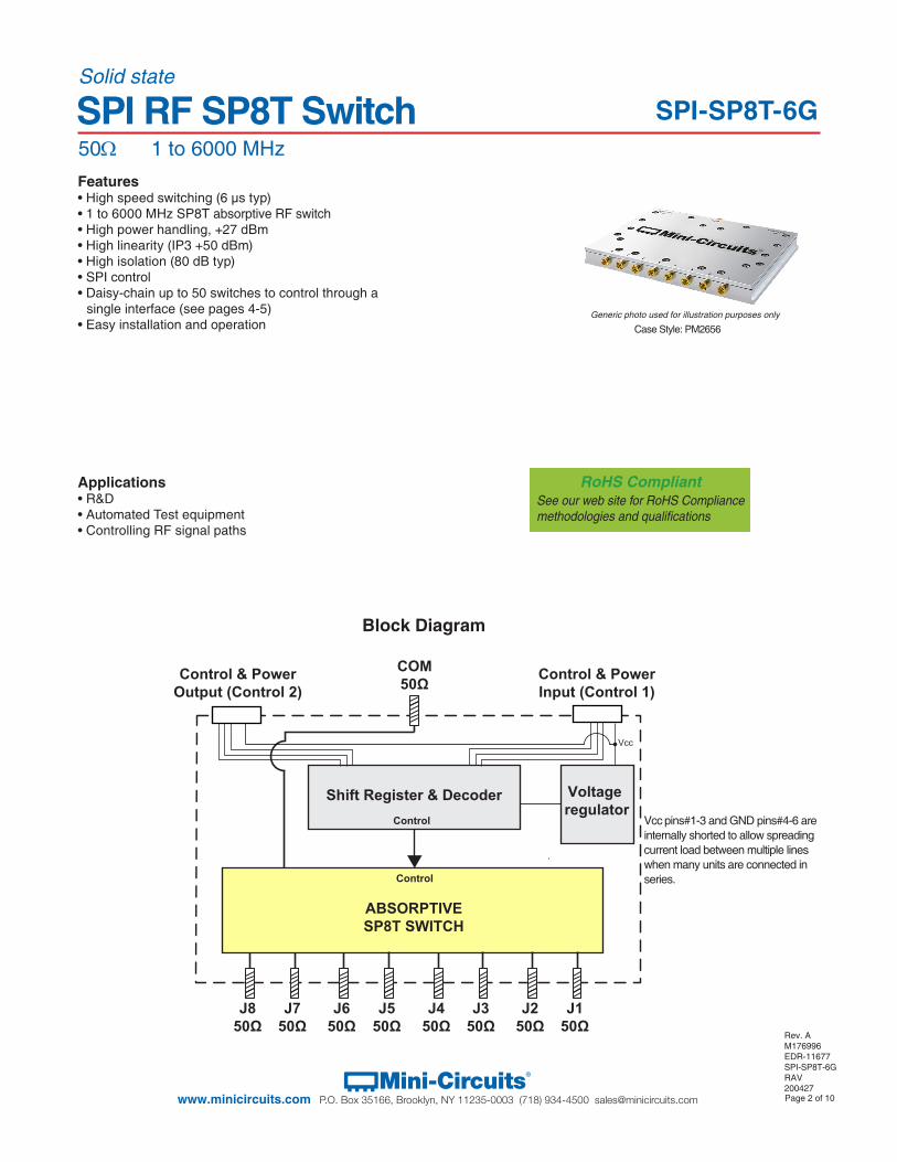
T:\catalog spec\Portable Test Equipment\RFSW\Visio files\xxxx-63 diagrams\SPI-SP8T-63_Diagram_X1.ai
Control & PowerInput (Control 1)
Shift Register & DecoderControl
COM50ΩControl & Power
Output (Control 2)
Voltage regulator
J850Ω
J750Ω
J550Ω
J650Ω
J450Ω
J350Ω
J250Ω
J150Ω
Control
ABSORPTIVESP8T SWITCH
Vcc
Block Diagram
Vcc pins#1-3 and GND pins#4-6 are internally shorted to allow spreading current load between multiple lines when many units are connected in series.
Generic photo used for illustration purposes only

Page 3 of 10Mini-Circuits®
www.minicircuits.com P.O. Box 35166, Brooklyn, NY 11235-0003 (718) 934-4500 [email protected]
SPI-SP8T-6GSPI RF SP8T Switch
Parameter Port Conditions Min. Typ. Max. Units
Operating Frequency 1 6000 MHz
Insertion Loss COM to active ports 1-81 to 3000 MHz − 3.2 5.0
dB3000 to 6000 MHz − 4.7 6.5
Isolation
Between any two ports of J1 to J8
1 to 3000 MHz 70 95 −
dB3000 to 6000 MHz 65 90 −
COM to any terminated port1 to 3000 MHz 65 90 −
3000 to 6000 MHz 60 85 −
VSWR
COM port 1 to 3000 MHz − 1.25 −
:1
3000 to 6000 MHz − 1.40 −
Any port connected to COM1 to 3000 MHz − 1.25 −
3000 to 6000 MHz − 1.45 −
Any terminated port1 to 3000 MHz − 1.10 −
3000 to 6000 MHz − 1.25 −
Power Input @1 dB Compression 1,2 COM to any active port 1 to 6000 MHz 30 − − dBm
IP3 3 COM to any active port 10 to 6000 MHz − 50 − dBm
Switching time 4 − 1 to 6000 MHz − 6 − µs
Operating RF Input Power
COM to any active port Hot Switching − − +17
dBmAny terminated port − − − +17
COM to any active port Through path 1 − − +27
Control Control is via SPI in at Control In port. Control Out can be used to connect multiple units in a ‘Daisy chain’ without additional controls
RF Electrical Specifications @ +25°C
Absolute Maximum RatingsOperating Temperature 0°C to 50°C
Storage Temperature -20°C to 60°C
DC supply voltage max. 26V
Control input line max. 6V
Max supply current per pin 800 mA
RF power @ into inactive (internal termination) port +20 dBm
RF power @ 1 -10 MHz into COM or active port +25 dBm
RF power @ 10 -6000 MHz into COM or active port +30 dBm
DC voltage @ RF Ports 16V
Permanent damage may occur if any of these limits are exceeded. Operating in the range between operating power limits and absolute maximum ratings for extended periods of time may result in reduced life and reliability.
ConnectionsRF Switch (J1 to J8, COM) (SMP male)
Power & Control in (Control in)* (Hirose DF11 10 pin Connector) 5
Power & Control out (Control out)** (Hirose DF11 10 pin Connector) 5
Pin Number Function
1 - 3 Vcc In
4 - 6 GND
7 Data In
8 Clock In
9 LE In
10 Lock in
* Control in Pin Connections
Pin Number Function
1 - 3 Vcc out
4 - 6 GND
7 Data Out
8 Clock Out
9 LE Out
10 Lock Out
** Control out Pin Connections
DC Electrical SpecificationsParameter Min. Typ. Max. Units
Vcc, Supply Voltage 5 — 24 VLoad on Vcc between In and Out ports — 0.05 — Ω
Icc, Supply Current
@24V — 7 —mA
@5V — 7 —Control Input Low -0.3 — +0.6 VControl Input High 2.0 — 5.5 VControl Current — 400 — µA
1 Max operating power degrades linearly below 10 MHz to +22 dBm at 1 MHz. 2 Note absolute maximum ratings in table below3 Tested with 1 MHz span between signals, +5 dBm per tone.4 Tested Latch Enable(LE) signal to 90% RF signal at RF port
5 Mating connector is Hirose DF11-10DS-2C(20)

Page 4 of 10Mini-Circuits®
www.minicircuits.com P.O. Box 35166, Brooklyn, NY 11235-0003 (718) 934-4500 [email protected]
SPI-SP8T-6GSPI RF SP8T Switch
Table 1: Switch Logic TableA0 A1 A2 A3 Switch State1 0 1 0 Com<->J1
1 0 1 1 Com<->J2
1 0 0 1 Com<->J3
1 0 0 0 Com<->J4
0 0 1 0 Com<->J5
0 0 1 1 Com<->J6
0 0 0 1 Com<->J7
0 0 0 0 Com<->J8
The SPI-SP8T-6G serial interface consists of 4 control bits per unit that select the desired switch state, as shown in Table 1: Switch Logic Table.
The serial interface is a 4-bit serial in, parallel-out shift register buffered by a transparent latch.It is controlled by three-wire SPI protocol using Data, Clock, and Latch Enable (LE) and an additional Lock for added noise immunity and increased exibility in controlling the units. All signal voltages are compatible with TTL and LVTTL. The Data and Clock inputs allow data to be serially entered into the shift register, a process that is independent of the state of the LE input.
The LE input controls the latch. When LE is HIGH, the latch is transparent and the contents of the serial shift reg-ister control the switch. When LE is brought LOW, data in the shift register is latched.
Lock is used to lock the current state of the switch regardless of LE state or shift register, while allowing the LE to pass to other switches in the chain. If Lock is at logic HIGH the switch will respond to LE normally, when Lock is at logic LOW the switch will not respond to LE. If Lock is not required it can be kept constantly at logic high.
The shift register should be loaded while LE is held LOW to prevent the switch state from changing as data is en-tered. If multiple units are connected in series, data for all units should be entered before raising the LE to prevent switches assuming unanticipated states. Thus for example if three units are connected in daisy chain all 12 bits of control should be entered before raising the LE (see figures 2-4 for connecting units in daisy chain).
The LE input should then be toggled HIGH and brought LOW again, latching the new data. The timing for this operation is defined by Figure 1: Serial Interface Timing Diagram and Table 2: Serial Interface AC Characteristics.
Note: 1. LE is connected in parallel to all units in a daisy chain using the switches internal buffers to prevent control current from increasing as more units are connected.
Control Interface
Figure 1: Serial Interface Timing Diagram
LE
Clock
Data A0
tLESUP
tSDSUP
tLLEPW
tSDHLD
A1A2A3
Table 2. Serial Interface AC Characteristics
Symbol Parameter Min. Max. Units
fclk Serial data clock frequency 20 MHz
tclkH Serial clock HIGH time 8 ns
tclkL Serial clock LOW time 14 ns
tLESUP LE set-up time after last clock rising edge 8 ns
tLEPW LE minimum pulse width 8 ns
tSDSUPSerial data set-up time before clock rising edge 8 ns
tSDHLDSerial data hold time after clock falling edge 1 ns

Page 5 of 10Mini-Circuits®
www.minicircuits.com P.O. Box 35166, Brooklyn, NY 11235-0003 (718) 934-4500 [email protected]
SPI-SP8T-6GSPI RF SP8T Switch
J1 to J8
SPI-SP8T-6G (Switch 1)
Control in Control out
J1 to J8
SPI-SP8T-6G (Switch 2)
J1 to J8
SPI-SP8T-6G (Switch 3)
J1 to J8
SPI-SP8T-6G (Switch 50)
Control in Control out Control in Control out Control in Control out
SPI
Power
SPI
Power
SPI
Power
COM COM COM COM
5V / 24V DC power supply
SPI Master
Figure 2: Connection diagram for multiple units in series
A0(SW3)
LE
Clock
Data A1(SW3)A2(SW3)A3(SW3)A0(SW2)A1(SW2)A2(SW2)A3(SW2)A0(SW1)A1(SW1)A2(SW1)A3(SW1)
Command for Switch 1 Command for Switch 2 Command for Switch 3
Figure 3: Serial Interface Timing Diagram for 3 units in series
Figure 4: Example of command for 3 switches in series
1
LE
Clock
Data 00000110 10 1
Set Switch 3 to COM->1 state Set Switch 2 to COM->8 state Set Switch 1 to COM->4 state
Control Interface (Daisy Chain)

Page 6 of 10Mini-Circuits®
www.minicircuits.com P.O. Box 35166, Brooklyn, NY 11235-0003 (718) 934-4500 [email protected]
SPI-SP8T-6GSPI RF SP8T Switch
Typical Performance Curves
1.0
2.0
3.0
4.0
5.0
6.0
0 1000 2000 3000 4000 5000 6000
Inse
rtio
n Lo
ss (d
B)
Frequency (MHz)
Insertion Loss over Temperature
@0°C@+25°C@+50°C
1.0
2.0
3.0
4.0
5.0
6.0
0 1000 2000 3000 4000 5000 6000
Inse
rtio
n Lo
ss (d
B)
Frequency (MHz)
Insertion Loss at Ports J1-J8 vs. Frequency
J1 J2
J3 J4
J5 J6
J7 J8
Frequency (MHz) Frequency (MHz)
1.0
1.2
1.4
1.6
1.8
2.0
0 1000 2000 3000 4000 5000 6000
VS
WR
(:1)
Frequency (MHz)
Internal Term. VSWR over Temp.
@0°C@+25°C@+50°C
Frequency (MHz)Frequency (MHz)
Frequency (MHz)
1.0
1.2
1.4
1.6
1.8
2.0
0 1000 2000 3000 4000 5000 6000
VS
WR
(:1)
Frequency (MHz)
Common Port VSWR over Temp.
@0°C@+25°C@+50°C
1.0
1.2
1.4
1.6
1.8
2.0
0 1000 2000 3000 4000 5000 6000
VS
WR
(:1)
Frequency (MHz)
Active Port VSWR over Temp.
@0°C@+25°C@+50°C

Page 7 of 10Mini-Circuits®
www.minicircuits.com P.O. Box 35166, Brooklyn, NY 11235-0003 (718) 934-4500 [email protected]
SPI-SP8T-6GSPI RF SP8T Switch
Typical Performance Curves (Continued)
Frequency (MHz)Frequency (MHz)
Frequency (MHz) Frequency (MHz)
Frequency (MHz)
40
60
80
100
120
140
0 1000 2000 3000 4000 5000 6000
Isol
atio
n (d
B)
Frequency (MHz)
Isolation Com to Port J1 with J2 active over Temp.
@0°C@+25°C@+50°C
40
60
80
100
120
140
0 1000 2000 3000 4000 5000 6000
Isol
atio
n (d
B)
Frequency (MHz)
Isolation Com to Port J1-J8 vs. Frequency
J1 J2 J3 J4
J5 J6 J7 J8
40
60
80
100
120
140
0 1000 2000 3000 4000 5000 6000
Isol
atio
n (d
B)
Frequency (MHz)
Isolation Port 2 to Port 1 Isolation over temp.
@0°C@+25°C@+50°C
40
60
80
100
120
140
0 1000 2000 3000 4000 5000 6000
Isol
atio
n (d
B)
Frequency (MHz)
Isolation Port to Port vs. Frequency
port 2 to 1 port 3 to 2 port 4 to 3 port 5 to 4
port 6 to 5 port 7 to 6 port 8 to 7 port 1 to 8
40
45
50
55
60
65
0 1000 2000 3000 4000 5000 6000
Isol
atio
n (d
B)
Frequency (MHz)
Input IP3
@ Port 8
@ Port 1

Page 8 of 10Mini-Circuits®
www.minicircuits.com P.O. Box 35166, Brooklyn, NY 11235-0003 (718) 934-4500 [email protected]
SPI-SP8T-6GSPI RF SP8T Switch
Outline Drawing (PM2656)
inchmmOutline Dimensions ( )
A B C D E F G H J KWT.
GRAMS
3.270 3.680 0.400 0.205 0.450 0.190 0.500 2.560 0.060 0.100180
83.06 93.47 10.16 5.21 11.43 4.83 12.70 65.02 1.52 2.54
98-PM Rev. D May 03, 2020 M171688 (R94372) File: 98-PM(D).doc Sheet 2 of 3 This document and its contents are the property of Mini-Circuits
Case Style PMOutline Dimensions
PM2656
Notes: 1. Case material: Aluminum alloy. 2. Case finish for RoHS Case Styles: Clear chemical conversion coating, non-chrome or trivalent chrome based.
CASE# A B C D E F G H J K WT.
PM2656 3.270 (83.06)
3.680 (93.47)
.400 (10.16)
.205 (5.21)
.450 (11.43)
.190 (4.83)
.500 (12.70)
2.560 (65.02)
.060 (1.52)
.100 (2.54) 180
Dimensions are in inches (mm). Tolerances: 2PL. +/- .03; 3PL. +/- .015

Page 9 of 10Mini-Circuits®
www.minicircuits.com P.O. Box 35166, Brooklyn, NY 11235-0003 (718) 934-4500 [email protected]
SPI-SP8T-6GSPI RF SP8T SwitchRecommended AccessoriesSeveral optional cable accessories with and without interface connector are available with the SPI-SP8T-6G.
Cable P/N Cable Length Wire Gauge Cable connectors Recommended useCBL-DF11-3FFD+ 3 ft (0.91 m) 30 AWG Hirose DF11-10DS-2C(20) on each end Connect between switches in series
CBL-DF11-3FPD+ 3 ft (0.91 m) 30 AWG Hirose DF11-10DS-2C(20) on one end, pigtail (bare wires) on the other
Connect SPI-SP8T-6G switch to customer control board and power
All cables are shielded and can handle the power draw of up to 50 switches in series.
CBL-DF11-3FPD+ Control Cable
Pin Number Function Description Pigtail Wire Color
1 Vcc Supply Voltage WHITE2 Vcc Supply Voltage BLACK3 Vcc Supply Voltage RED4 GND Ground connection GREEN5 GND Ground connection YELLOW6 GND Ground connection BLUE7 Data Data for SPI BROWN
8 Clock Clock for SPI ORANGE
9 LE Latch Enable for SPI GRAY10 Lock Lock for SPI VIOLET
J1
CBL-DF11-3FFD+ Control Cable
J1 Pin Number
J2 Pin Number Function Description
1 1 Vcc Supply Voltage2 2 Vcc Supply Voltage3 3 Vcc Supply Voltage4 4 GND Ground connection5 5 GND Ground connection6 6 GND Ground connection7 7 Data Data for SPI
8 8 Clock Clock for SPI
9 9 LE Latch Enable for SPI 10 10 Lock Lock for SPI
J2J1

Page 10 of 10Mini-Circuits®
www.minicircuits.com P.O. Box 35166, Brooklyn, NY 11235-0003 (718) 934-4500 [email protected]
SPI-SP8T-6GSPI RF SP8T Switch
Ordering, Pricing & Availability Information see our web site
Model DescriptionSPI-SP8T-6G SPI RF SP8T Switch
Additional NotesA. Performance and quality attributes and conditions not expressly stated in this specification document are intended to be excluded and do not form a part of this
specification document. B. Electrical specifications and performance data contained in this specification document are based on Mini-Circuit’s applicable established test performance criteria and
measurement instructions. C. The parts covered by this specification document are subject to Mini-Circuits standard limited warranty and terms and conditions (collectively, “Standard Terms”);
Purchasers of this part are entitled to the rights and benefits contained therein. For a full statement of the Standard Terms and the exclusive rights and remedies thereunder, please visit Mini-Circuits’ website at www.minicircuits.com/MCLStore/terms.jsp
Optional Accessories DescriptionCBL-DF11-3FFD+ 3 ft. Hirose DF11 (female-female) cable assembly (SPI)
CBL-DF11-3FPD+ 3 ft. Hirose DF11 (female-pigtail) cable assembly (SPI)
SMPF-SF50+ SMP Female to SMA Female Adapter