product specification g1212x03 series - cct.com.my · product specification g1212x03 series crystal...
TRANSCRIPT
Product Specification
G1212X03 series
Crystal Clear Technology sdn. bhd. 16Jalan TP5—Taman Perindustrian Sime UEP 47600 Subang Jaya—Selangor DE Malaysia. T: +603 80247099 F: +603 80247098
CRYSTAL CLEAR TECHNOLOGY SDN. BHD.
Spec. No: G1212x03xxx00 REV 1.0
1
1.0 Table of Contents
Page
1. Table of Contents 1
2. Record of revision 2
3. General specification 3
4. Absolute maximum ratings 4
5. Electrical characteristics 4
6. Environmental requirement 4
7. LCD specification 5 ~ 7
8. Interface 8
9. Functional Description 9 ~ 25
10. Quality assurance 25 ~ 31
11. Precautions in use LCM 32 ~ 33
12. Outline drawing 24 ~ 35
CRYSTAL CLEAR TECHNOLOGY SDN. BHD.
Spec. No: G1212x03xxx00 REV 1.0
2
2.0 Record of revision
Rev Date Item Page Comment Originator Checked By
1.0
21/03/09 Initial Release
Khairiah
Azhar
CRYSTAL CLEAR TECHNOLOGY SDN. BHD.
Spec. No: G1212x03xxx00 REV 1.0
3
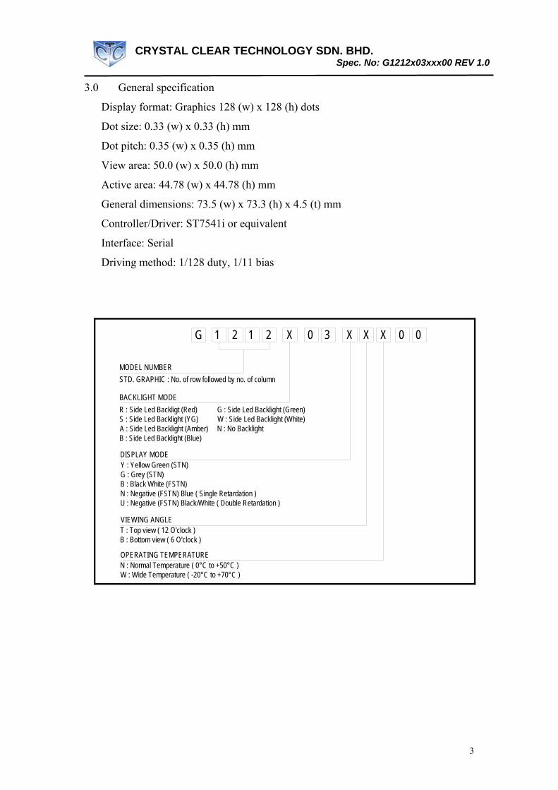
3.0 General specification
Display format: Graphics 128 (w) x 128 (h) dots
Dot size: 0.33 (w) x 0.33 (h) mm
Dot pitch: 0.35 (w) x 0.35 (h) mm
View area: 50.0 (w) x 50.0 (h) mm
Active area: 44.78 (w) x 44.78 (h) mm
General dimensions: 73.5 (w) x 73.3 (h) x 4.5 (t) mm
Controller/Driver: ST7541i or equivalent
Interface: Serial
Driving method: 1/128 duty, 1/11 bias
OPERATING TEMPERATUREN : Normal Temperature ( 0°C to +50°C )W : Wide Temperature ( -20°C to +70°C )
STD. GRAPHIC : No. of row followed by no. of column
Y : Yellow Green (STN)G : Grey (STN)B : Black White (FSTN)N : Negative (FSTN) Blue ( Single Retardation )U : Negative (FSTN) Black/White ( Double Retardation )
BACKLIGHT MODE
B : Bottom view ( 6 O'clock )T : Top view ( 12 O'clock )
DISPLAY MODE
VIEWING ANGLE
MODEL NUMBER
G 1 2 1 2 X 0 3 X X X 0 0
G : Side Led Backlight (Green)W : Side Led Backlight (White)N : No Backlight
R : Side Led Backligt (Red)S : Side Led Backlight (YG)A : Side Led Backlight (Amber)B : Side Led Backlight (Blue)
CRYSTAL CLEAR TECHNOLOGY SDN. BHD.
Spec. No: G1212x03xxx00 REV 1.0
4
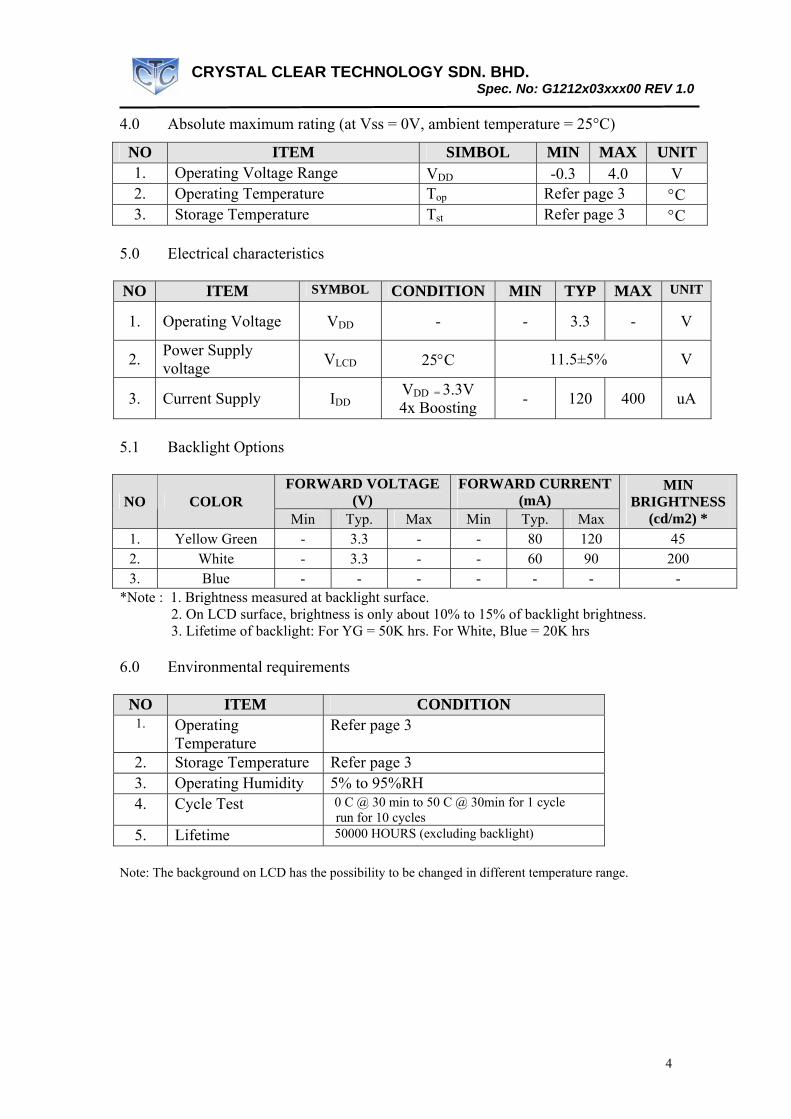
4.0 Absolute maximum rating (at Vss = 0V, ambient temperature = 25°C)
NO ITEM SIMBOL MIN MAX UNIT 1. Operating Voltage Range VDD -0.3 4.0 V 2. Operating Temperature Top Refer page 3 °C 3. Storage Temperature Tst Refer page 3 °C
5.0 Electrical characteristics
NO ITEM SYMBOL CONDITION MIN TYP MAX UNIT
1. Operating Voltage VDD - - 3.3 - V
2. Power Supply voltage VLCD 25°C 11.5±5% V
3. Current Supply IDD VDD = 3.3V 4x Boosting - 120 400 uA
5.1 Backlight Options
FORWARD VOLTAGE
(V) FORWARD CURRENT
(mA) NO COLOR Min Typ. Max Min Typ. Max
MIN BRIGHTNESS
(cd/m2) * 1. Yellow Green - 3.3 - - 80 120 45 2. White - 3.3 - - 60 90 200 3. Blue - - - - - - -
*Note : 1. Brightness measured at backlight surface. 2. On LCD surface, brightness is only about 10% to 15% of backlight brightness. 3. Lifetime of backlight: For YG = 50K hrs. For White, Blue = 20K hrs 6.0 Environmental requirements
NO ITEM CONDITION
1. Operating Temperature
Refer page 3
2. Storage Temperature Refer page 3 3. Operating Humidity 5% to 95%RH 4. Cycle Test 0 C @ 30 min to 50 C @ 30min for 1 cycle
run for 10 cycles 5. Lifetime 50000 HOURS (excluding backlight)
Note: The background on LCD has the possibility to be changed in different temperature range.

CRYSTAL CLEAR TECHNOLOGY SDN. BHD.
Spec. No: G1212x03xxx00 REV 1.0
5
7.0 LCD specification 7.1 Electro-optical characteristics (at ambient temperature = 25°C)
LCD TYPE UNIT
NO ITEM SYMBOL CONDITION STN YG
STN GREY
STN -VE
BLUE
FSTN +VE B/W
FSTN –VE
BLUE
FSTN -VE
TRUE B/W
FSTN -VE TRI
AXIS
REF.
1 Operating Voltage (Volt)
VLCD θ = 0 Cr = max 8.0 ± 5% 7.1.1
θ x 1 +25 +20 +35 +25 +35 +35 +40 θ x 2 -25 -20 -35 -25 -35 -40 -40 θ y 1 -30 -25 -35 -30 -35 -35 -50
2 Viewing
Angle (Deg)
θ y 2
CR ≥ 2 VLCD = 14.7V
+30 +25 +35 +30 +35 +35 +30
7.1.2
3 Contrast Ratio CR
θ = 00 VLCD
=14.7V 3.0 2.3 6.0 3.0 6.0 20 20 7.1.3
Rise Time (Tr)
θ = 00 200
4 Response
Time (msec) Decay
Time (Td)
θ = 00 250
7.1.4
Note:
1. Viewing angle data is based on bottom view product by default. Should it be a top view product, values are then swap.
2. Contrast ratio is based on typical data when using white colour as backlight. 3. Equipment Used Eldim; Ez Contrast 120R , Spot Size = 2mm

CRYSTAL CLEAR TECHNOLOGY SDN. BHD.
Spec. No: G1212x03xxx00 REV 1.0
6
NO CHARACTERISTICS DEFINITIONS 7.1.1
Definition of Operating Voltage (VLCD)
VLCD 1/F VLCD : Operating Voltage F : Frame Frequency
7.1.2
Definition of Viewing Angle
TOP θ REAR LEFT RIGHT FRONT BOTTOM REAR (θy2) LEFT(θx2) RIGHT(θx1) FRONT (θy1)

CRYSTAL CLEAR TECHNOLOGY SDN. BHD.
Spec. No: G1212x03xxx00 REV 1.0
7
7.1.3
Definition of Contrast Ratio
NON-SELECT WAVE BRIGHTNESS (%) SELECT WAVE b a OPERATION VOLTAGE Contrast Ratio = Brightness of non-selected state (b) Brightness of selected state (a) Conditions (a) Operating Voltage: VLCD (b) Temperature: 25°C (c) Viewing Angle, θ = 0o
7.1.4
Response Time
Luminance (%) 90 10 Tr: Measured between 10% and 90% of LCD segment maximum response with VON. Td: With voltage switches to zero and the instant LCD segment reaches 10% of its maximum response.
Td TrTime

CRYSTAL CLEAR TECHNOLOGY SDN. BHD.
Spec. No: G1212x03xxx00 REV 1.0
8
8.0 Interface
8.1 Display Driver ST7541 OR EQUIVALENT
8.3 Pin No Symbol Description
1 A Backlight Supply
2 K Backlight Ground
3 RST Reset pin
4 SDA IIC Data bus
5 SCL IIC Clock bus
6 VDD Logic Power Supply
7 VSS Ground
8 VOUT Booster Output Voltage
9 V4 LCD Driving Voltage
10 V3 LCD Driving Voltage
11 V2 LCD Driving Voltage
12 V1 LCD Driving Voltage
13 V0 LCD Driving Voltage
CRYSTAL CLEAR TECHNOLOGY SDN. BHD.
Spec. No: G1212x03xxx00 REV 1.0
9
9.0 Functional Descriptions
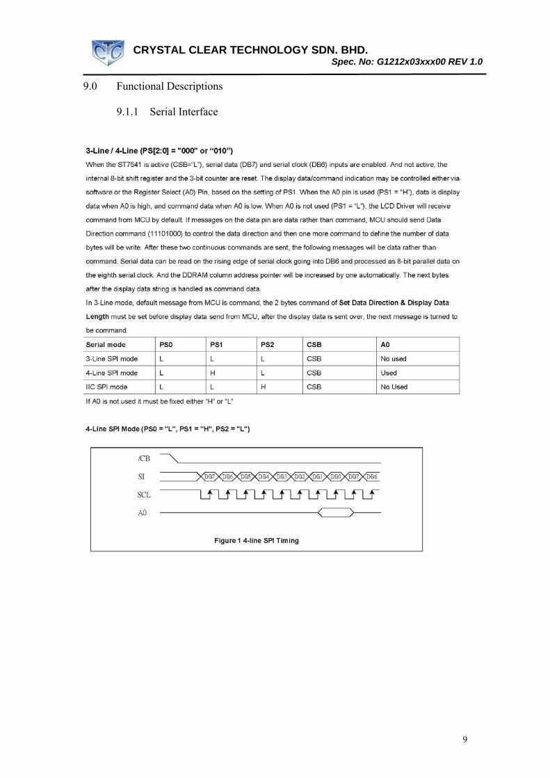
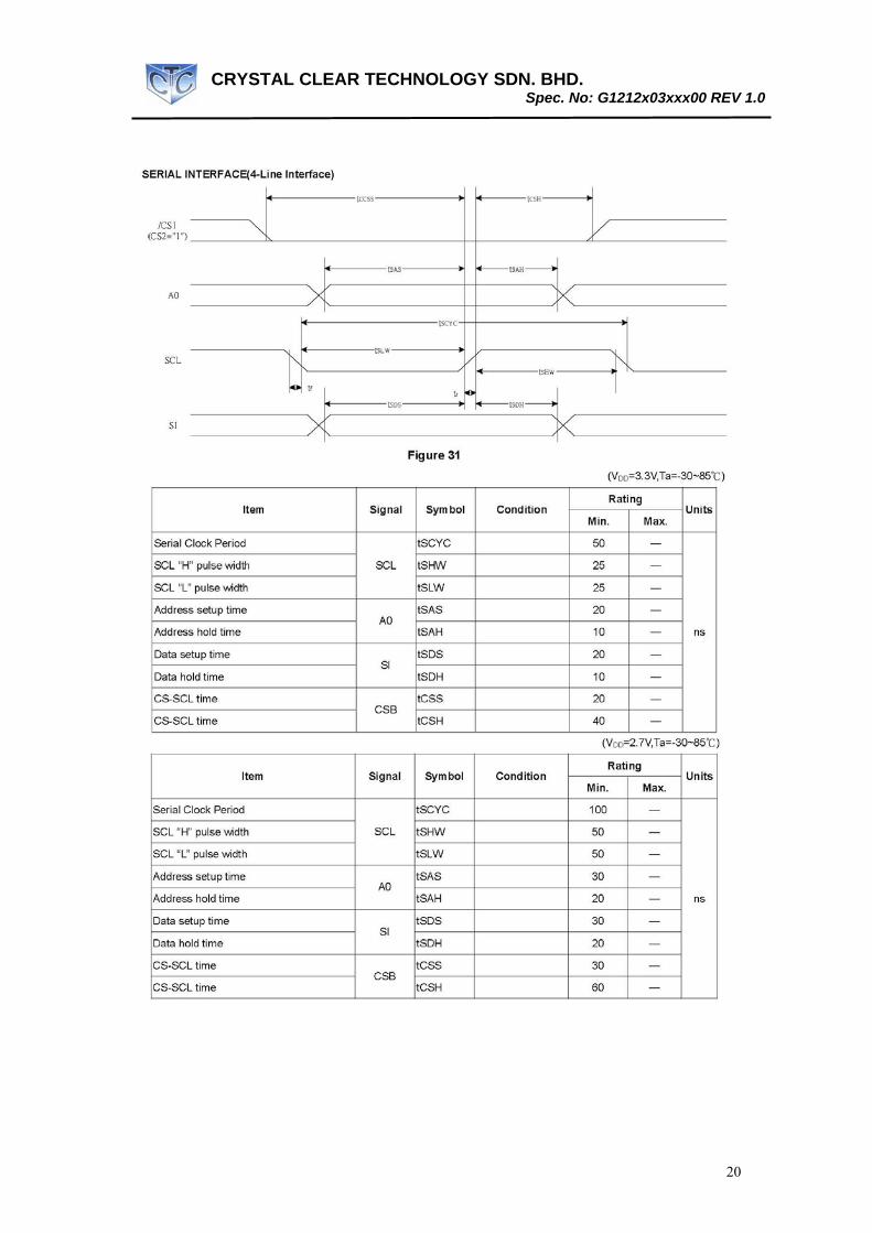
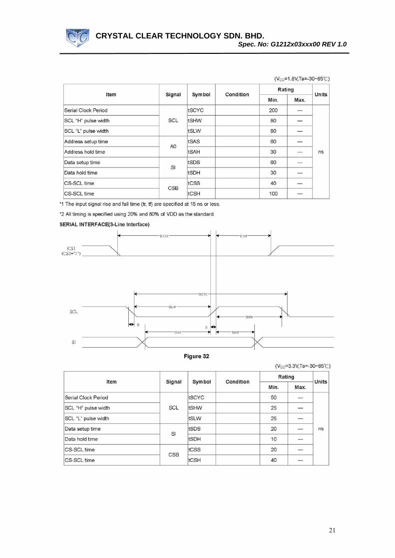
9.1.1 Serial Interface

CRYSTAL CLEAR TECHNOLOGY SDN. BHD.
Spec. No: G1212x03xxx00 REV 1.0
10

CRYSTAL CLEAR TECHNOLOGY SDN. BHD.
Spec. No: G1212x03xxx00 REV 1.0
11
9.1.2 IIC Interface (PS0= ‘L’, PS1 = ‘L’, PS2 = ‘H’)
CRYSTAL CLEAR TECHNOLOGY SDN. BHD.
Spec. No: G1212x03xxx00 REV 1.0
12
CRYSTAL CLEAR TECHNOLOGY SDN. BHD.
Spec. No: G1212x03xxx00 REV 1.0
13
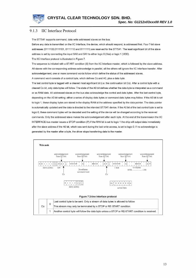
9.1.3 IIC Interface Protocol
CRYSTAL CLEAR TECHNOLOGY SDN. BHD.
Spec. No: G1212x03xxx00 REV 1.0
14
CRYSTAL CLEAR TECHNOLOGY SDN. BHD.
Spec. No: G1212x03xxx00 REV 1.0
15
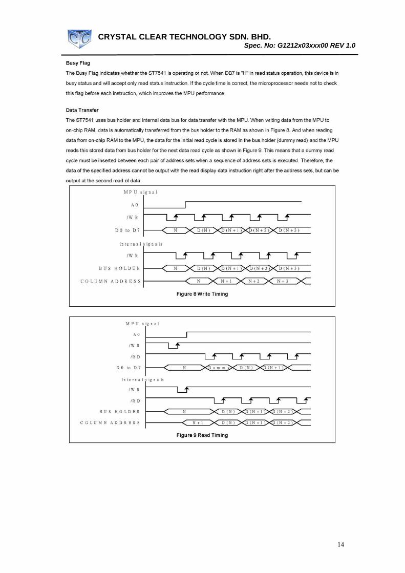
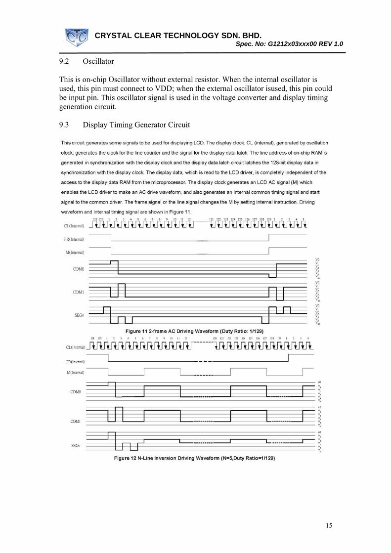
9.2 Oscillator This is on-chip Oscillator without external resistor. When the internal oscillator is used, this pin must connect to VDD; when the external oscillator isused, this pin could be input pin. This oscillator signal is used in the voltage converter and display timing generation circuit. 9.3 Display Timing Generator Circuit
CRYSTAL CLEAR TECHNOLOGY SDN. BHD.
Spec. No: G1212x03xxx00 REV 1.0
16
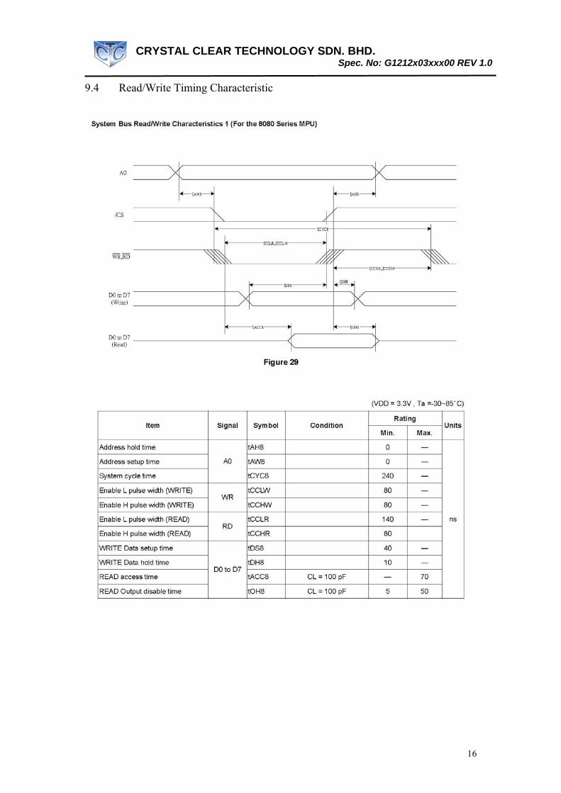
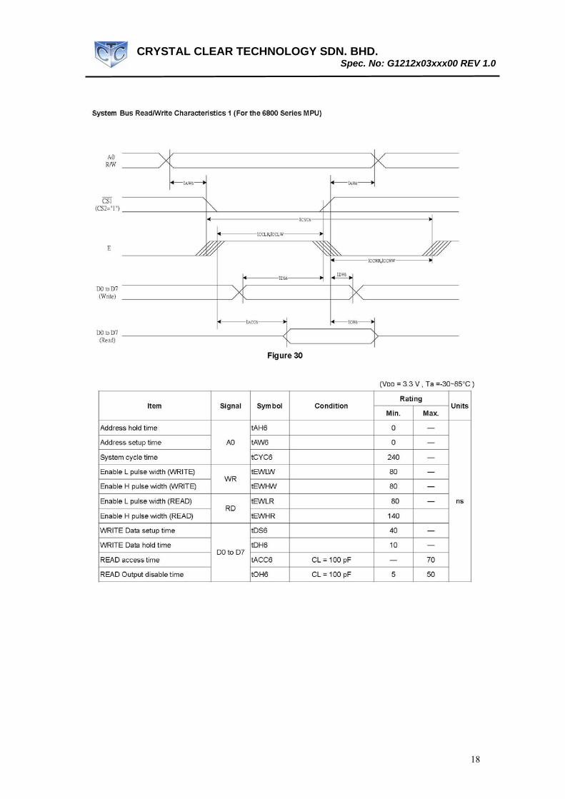
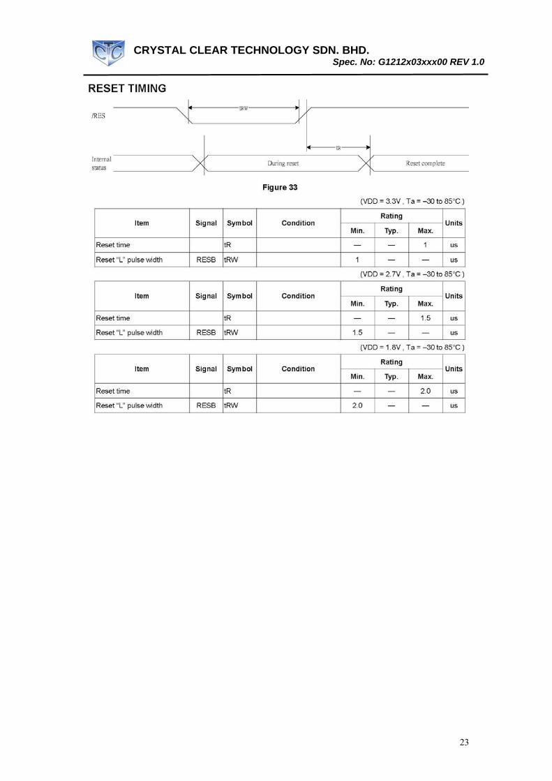
9.4 Read/Write Timing Characteristic

CRYSTAL CLEAR TECHNOLOGY SDN. BHD.
Spec. No: G1212x03xxx00 REV 1.0
17
CRYSTAL CLEAR TECHNOLOGY SDN. BHD.
Spec. No: G1212x03xxx00 REV 1.0
18

CRYSTAL CLEAR TECHNOLOGY SDN. BHD.
Spec. No: G1212x03xxx00 REV 1.0
19
CRYSTAL CLEAR TECHNOLOGY SDN. BHD.
Spec. No: G1212x03xxx00 REV 1.0
20
CRYSTAL CLEAR TECHNOLOGY SDN. BHD.
Spec. No: G1212x03xxx00 REV 1.0
21

CRYSTAL CLEAR TECHNOLOGY SDN. BHD.
Spec. No: G1212x03xxx00 REV 1.0
22
CRYSTAL CLEAR TECHNOLOGY SDN. BHD.
Spec. No: G1212x03xxx00 REV 1.0
23

CRYSTAL CLEAR TECHNOLOGY SDN. BHD.
Spec. No: G1212x03xxx00 REV 1.0
24
9.5 Application Circuit

CRYSTAL CLEAR TECHNOLOGY SDN. BHD.
Spec. No: G1212x03xxx00 REV 1.0
25
10.0 Quality Assurance 10.1 ZONE DEFINITION
10.2 REJECTION CRITERIA
10.2.1 DIMENSIONAL DEFECTS
Defect Category
Defect Description Criterion Drawing Specification
Glass Size Dimensions of LCD, do not conform to the drawing
Reject Refer to LCD Physical Dimension Drawing
Perimeter Seal Extension
Perimeter seal epoxy enters the effective viewing area
Reject
End Seal Size
Size of end seal does not meet drawing specification
Reject Refer to LCD Physical Dimension Drawing
EFFECTIVE VIEWING AREA ZONE A ZONE B (Outside Viewing Area) ZONE C (Sealing Area)

CRYSTAL CLEAR TECHNOLOGY SDN. BHD.
Spec. No: G1212x03xxx00 REV 1.0
26
10.2.2 VISUAL DEFECTS
Defect Category Defect Description Criterion Drawing Specification
Fracture A type of glass breakage containing running cracks. Inspectors should attempt to remove it with fingernail. If removed, evaluate as chip
Reject – if the size is > 30% of the contact ledge width.
Defect Category Defect Description Criterion Drawing Specification
Chip Chip in cross over area
1) Reject - if the chip causes crossover dot to be exposed 2) Chip on outside edge of the glass plate but is greater than 50% of glass thickness at crossover dot is reject able.
Chip Chip in contact pad area
Accept if:- a) X ≤ 2.0mm b) Y ≤ 0.5mm c) Z disregard
Chip in non-contact pad area
Accept if:- a) X ≤ 6.0mm b) Y ≤ 1.0mm c) Z disregard
Chip
Epoxy of crossover dot exposed
X
Y Z
Y
X
Y
ZX

CRYSTAL CLEAR TECHNOLOGY SDN. BHD.
Spec. No: G1212x03xxx00 REV 1.0
27
Chip in perimeter seal area
Accept if:- a) Y ≤ 1/3 of perimeter seal width (W) b) X ≤ 3.0mm c) Z disregard d) X and Y not touch crossover dot
Corner Chip Corner chip within seal area
Accept if:- a) X ≤ 1/3 of perimeter seal width (W) b) Y ≤ 1/3 of perimeter seal width (W) c) Z disregard
Defect Category Defect Description Criterion Drawing Specification
Corner chip not effecting contact pad / ITO
Accept if:- a) XY ≤ 4mm2 AND b) Y ≤ D and X ≤ 2.0mm c) Z disregard
Corner chip effecting contact pad / ITO
A) Accept if:- a) XY ≤ 4mm2 AND b) Y ≤ D and X ≤ 2.0mm B) Accept if:- a) X1 ≤ 2.0mm b) Y1 ≤ 0.5mm Z disregard
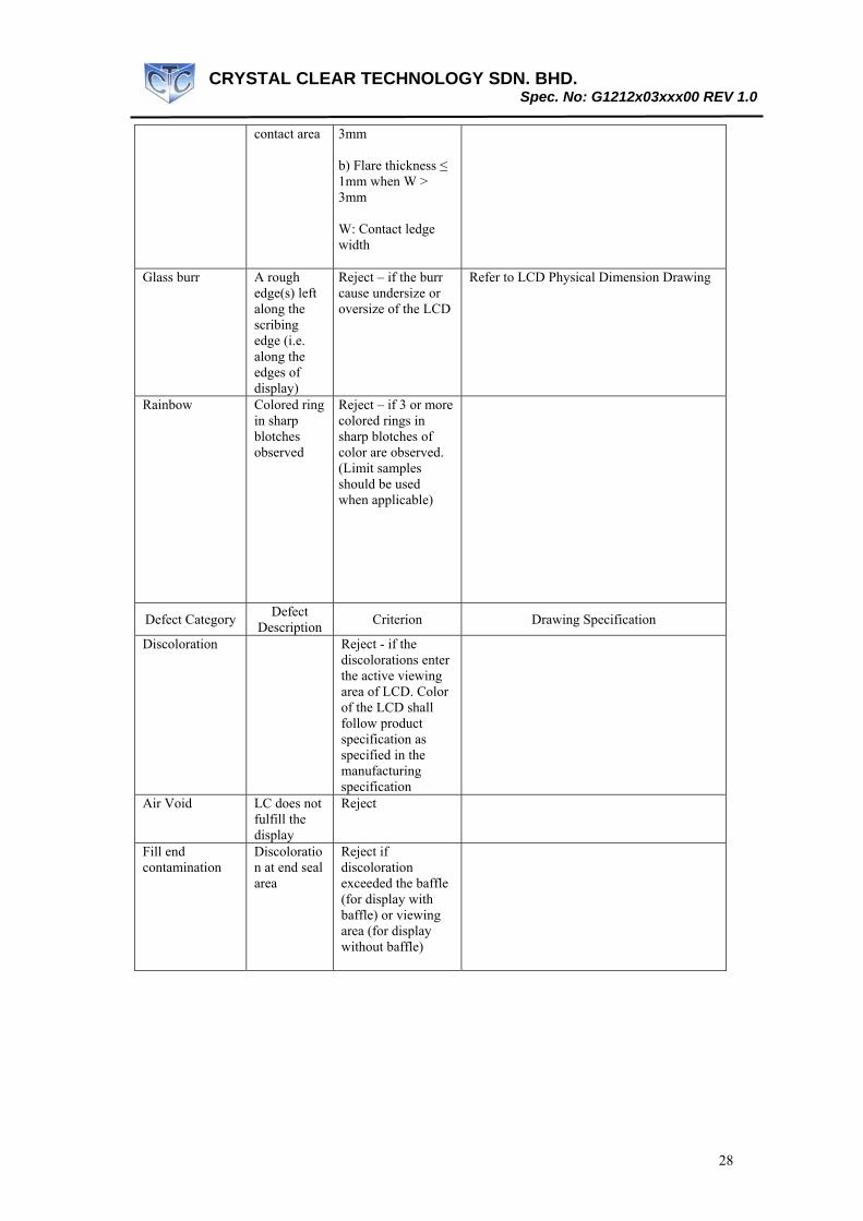
Glass flare A thin layer of glass flare at
Accept if:- a) Flare thickness ≤ ¼ W when W ≤
Z
X Y
W
Z
Y
X
Y X
Z
W
Y X
D
Z
D
X
X1 Y Y1
A B
Z
CRYSTAL CLEAR TECHNOLOGY SDN. BHD.
Spec. No: G1212x03xxx00 REV 1.0
28
contact area 3mm b) Flare thickness ≤ 1mm when W > 3mm W: Contact ledge width
Glass burr A rough edge(s) left along the scribing edge (i.e. along the edges of display)
Reject – if the burr cause undersize or oversize of the LCD
Refer to LCD Physical Dimension Drawing
Rainbow Colored ring in sharp blotches observed
Reject – if 3 or more colored rings in sharp blotches of color are observed. (Limit samples should be used when applicable)
Defect Category Defect Description Criterion Drawing Specification
Discoloration Reject - if the discolorations enter the active viewing area of LCD. Color of the LCD shall follow product specification as specified in the manufacturing specification
Air Void LC does not fulfill the display
Reject
Fill end contamination
Discoloration at end seal area
Reject if discoloration exceeded the baffle (for display with baffle) or viewing area (for display without baffle)
CRYSTAL CLEAR TECHNOLOGY SDN. BHD.
Spec. No: G1212x03xxx00 REV 1.0
29
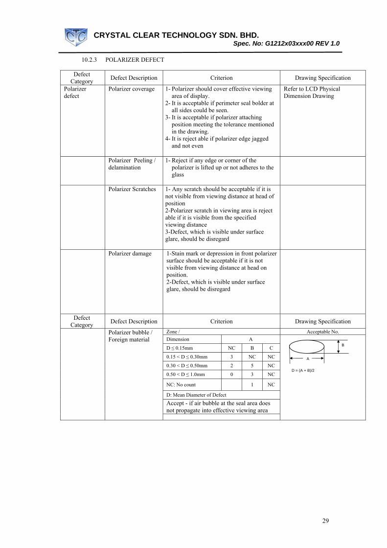
10.2.3 POLARIZER DEFECT
Defect Category Defect Description Criterion Drawing Specification
Polarizer defect
Polarizer coverage 1- Polarizer should cover effective viewing area of display.
2- It is acceptable if perimeter seal bolder at all sides could be seen.
3- It is acceptable if polarizer attaching position meeting the tolerance mentioned in the drawing.
4- It is reject able if polarizer edge jagged and not even
Refer to LCD Physical Dimension Drawing
Polarizer Peeling / delamination
1- Reject if any edge or corner of the polarizer is lifted up or not adheres to the glass
Polarizer Scratches 1- Any scratch should be acceptable if it is not visible from viewing distance at head of position 2-Polarizer scratch in viewing area is reject able if it is visible from the specified viewing distance 3-Defect, which is visible under surface glare, should be disregard
Polarizer damage 1-Stain mark or depression in front polarizer surface should be acceptable if it is not visible from viewing distance at head on position. 2-Defect, which is visible under surface glare, should be disregard
Defect Category Defect Description Criterion Drawing Specification
Zone / Acceptable No. Dimension A
D ≤ 0.15mm NC B C
0.15 < D ≤ 0.30mm 3 NC NC
0.30 < D ≤ 0.50mm 2 5 NC
0.50 < D ≤ 1.0mm 0 3 NC
NC: No count 1 NC
D: Mean Diameter of Defect Accept - if air bubble at the seal area does not propagate into effective viewing area
Polarizer bubble / Foreign material
A
B
D = (A + B)/2
CRYSTAL CLEAR TECHNOLOGY SDN. BHD.
Spec. No: G1212x03xxx00 REV 1.0
30
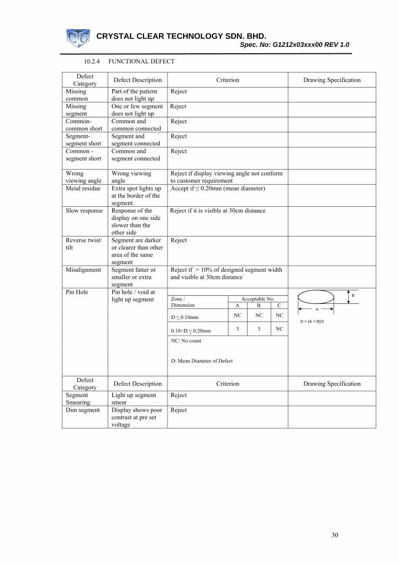
10.2.4 FUNCTIONAL DEFECT
Defect Category Defect Description Criterion Drawing Specification
Missing common
Part of the pattern does not light up
Reject
Missing segment
One or few segment does not light up
Reject
Common-common short
Common and common connected
Reject
Segment-segment short
Segment and segment connected
Reject
Common – segment short
Common and segment connected
Reject
Wrong viewing angle
Wrong viewing angle
Reject if display viewing angle not conform to customer requirement
Metal residue Extra spot lights up at the border of the segment.
Accept if ≤ 0.20mm (mean diameter)
Slow response Response of the display on one side slower than the other side
Reject if it is visible at 30cm distance
Reverse twist/ tilt
Segment are darker or clearer than other area of the same segment
Reject
Misalignment Segment fatter or smaller or extra segment
Reject if > 10% of designed segment width and visible at 30cm distance
Acceptable No. Zone /
Dimension A B C
D < 0.10mm NC NC NC
0.10<D < 0.20mm 3 3 NC
NC: No count
Pin Hole Pin hole / void at light up segment
D: Mean Diameter of Defect
Defect Category Defect Description Criterion Drawing Specification
Segment Smearing
Light up segment smear
Reject
Dim segment Display shows poor contrast at pre set voltage
Reject
A
B
D = (A + B)/2
CRYSTAL CLEAR TECHNOLOGY SDN. BHD.
Spec. No: G1212x03xxx00 REV 1.0
31
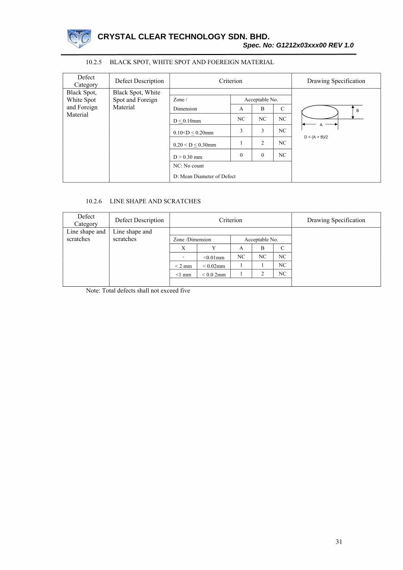
10.2.5 BLACK SPOT, WHITE SPOT AND FOEREIGN MATERIAL
Defect Category Defect Description Criterion Drawing Specification
Zone / Acceptable No.
Dimension A B C
D < 0.10mm NC NC NC
0.10<D < 0.20mm 3 3 NC
0.20 < D < 0.30mm 1 2 NC
D > 0.30 mm 0 0 NC
NC: No count
Black Spot, White Spot and Foreign Material
Black Spot, White Spot and Foreign Material
D: Mean Diameter of Defect
10.2.6 LINE SHAPE AND SCRATCHES
Defect Category Defect Description Criterion Drawing Specification
Zone /Dimension Acceptable No.
X Y A B C - <0.01mm
NC NC NC
< 2 mm
< 0.02mm
1 1 NC
<1 mm
< 0.0 2mm
1 2 NC
Line shape and scratches
Line shape and scratches
Note: Total defects shall not exceed five
A
B
D = (A + B)/2

CRYSTAL CLEAR TECHNOLOGY SDN. BHD.
Spec. No: G1212x03xxx00 REV 1.0
32
13. Precaution for using LCM
1. Liquid Crystal Display (LCD)
LCD is made up of glass, organic sealant, organic fluid and
polymer based polarizers. The following precautions should
be taken when handling.
b) Keep the temperature within the range of use and
storage. Excessive temperature and humidity
could cause polarization degredation, polarizer
peel off or bubble.
c) Do not contact the exposed polarizer with
anything harder than HB pencil lead. To clean
dust off the display surface, wipe gently with
cotton, chamois or other soft material soaked in
petroleum benzin.
d) Wipe off saliva or water drops immediately.
Contact with water over a long period of time
may cause polarizer deformation or colour
fading, while an active LCD with water
condensation on its surface will cause corrosion
of ITO electrodes.
e) Glass can be easily chipped or cracked from
rough handling, especially at corners and edges.
f) Do not drive LCD with DC voltage.
2. Liquid Crystal Display Modules.
2.1 Mechanical Considerations
LCM are assembled and adjusted with a high
degree of precision. Avoid excessive shocks and
do not make any alterations or modification. The
following should be noted.
a) Do not tamper in any way with the tabs
on the metal frame.
b) Do not modify the PCB by drilling
extra holes, changing its outline,
moving its component or modifying its
pattern.
c) Do not touch the elastomer connector,
especially insert a backlight panel (for
example, EL)
d) When mounting a LCM make sure that
the PCB is not under any stress such as
bending or twisting. Elastomer contacts
are very delicate and missing pixels
could result from slight dislocation of
any of the elements.
a) Avoid pressing on the metal bezel,
otherwise the elastomer connector
could be deformed and lose contact,
resulting in missing pixels.
2.2 Static Electricity
LCM contains CMOS LSI’s and the same
precaution for such devices should apply, namely
a) The operator should be grounded whenever
he/she comes into contact with the module.
Never touch any of the conductive parts
such as the LSI pads, the copper leads on the
PCB and the interface terminals with any
parts of the human body.
b) The modules should be kept in antistatic
bags or other containers to static for storage.
c) Only properly grounded soldering irons
should be used.
d) If an electric screwdriver is used, it should
be well grounded and shielded from
commutator spark.
e) The normal static prevention measures
should be observed for work clothes and
working benches, the latter conductive
(rubber) mat is recommended.
f) Since dry air is inductive to statics, a relative
humidity of 50-60% is recommended.
2.3 Soldering
a) Solder only to the I/O terminals.
b) Use only soldering irons with proper
grounding and no leakage.
c) Soldering temperature: 280 °C
d) Soldering time: 3 to 4 sec
e) Use eutectic solder with resin flux fill.
f) If flux is used, the LCD surface should be
covered to avoid flux spatters. Flux residue
should be removed afterwards.

CRYSTAL CLEAR TECHNOLOGY SDN. BHD.
Spec. No: G1212x03xxx00 REV 1.0
33
2.4 Operation
a) The contras can be adjusted by varying the
LCD driving voltage V0
b) Driving voltage should be kept within
specified range, excess voltage shortens
display life.
c) Response time increases with decrease in
temperature.
d) Display may turn black or dark blue at
temperature above its operational range, this
is (however not pressing on the viewing
area) may cause the segments to appear
“fractured”.
e) Mechanical disturbance during operation (
such as pressing on the viewing area) may
cause the segments to appear “fractured”.
2.5 Storage
If any fluid leaks out of the damage glass cell,
wash off any human part that comes into contact
with soap and water. Never swallow the fluid.
The toxicity is extremely low but caution should
be exercised at all the time.
2.6 Limited Warranty
Unless otherwise agreed between Crystal Clear
Technology and customer, Crystal Clear
Technology will replace or repair any of its LCD
and LCM which is found to be defective
electrically and visually when inspected in
accordance with Crystal Clear Technology
acceptance standards, for a period of one year
from date of shipment. Confirmation of such date
shall be based on freight documents. The
warranty liability of Crystal Clear Technology is
limited to repair and/or replacement on the terms
set forth above. Crystal Clear Technology will
not responsible for any subsequent or
consequential events.

CRYSTAL CLEAR TECHNOLOGY SDN. BHD.
Spec. No: G1212x03xxx00 REV 1.0
34
CRYSTAL CLEAR TECHNOLOGY SDN. BHD.
Spec. No: G1212x03xxx00 REV 1.0
35
Crystal Clear Technology 16 Jalan TP5—Taman Perindustrian Sime UEP
47600 Subang Jaya—Selangor DE Malaysia