product specification lp150e07 liquid crystal display ver. 0.4jul. 20. 2006 1 / 24 specification for...
TRANSCRIPT

Product Specification
1 / 24
LP150E07Liquid Crystal Display
Ver. 0.4 Jul. 20. 2006
SPECIFICATION
FOR
APPROVAL
Title 15.0” SXGA+ TFT LCD
BUYER Lenovo
MODEL
SUPPLIER LG.Philips LCD Co., Ltd.
*MODEL LP150E07
Suffix TL03
*When you obtain standard approval, please use the above model name without suffix
SIGNATURE DATE
/
/
/
Please return 1 copy for your confirmation withyour signature and comments.
( ◆ ) Preliminary Specification
( ) Final Specification
J. H. Lee / S.Manager
Product Engineering Dept.LG. Philips LCD Co., Ltd
APPROVED BY Signaure
REVIEWED BY
PREPARED BY
K.K.Jang / Manager
N.J. Seong / Engineer
Product Specification
2 / 24
LP150E07Liquid Crystal Display
Ver. 0.4 Jul. 20. 2006
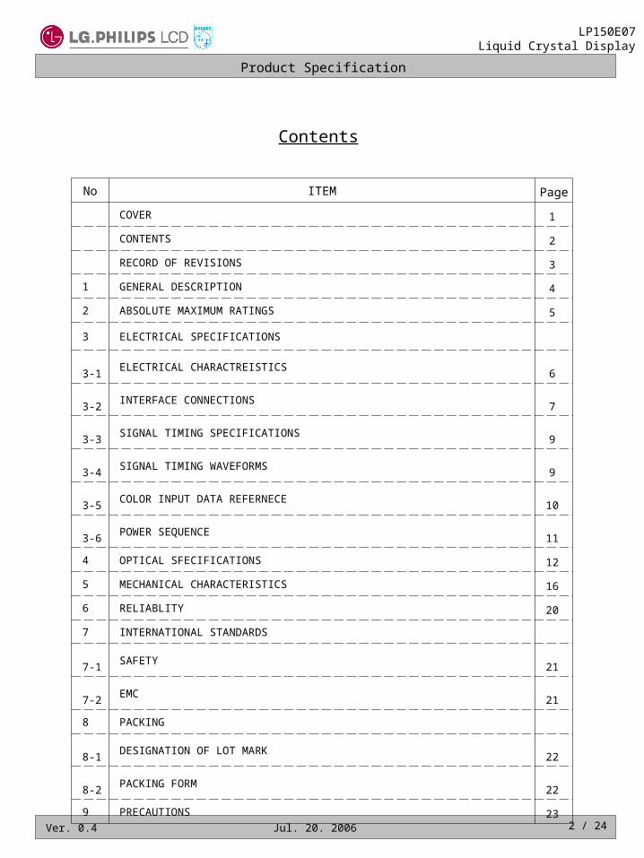
Contents
No ITEM Page
COVER 1
CONTENTS 2
RECORD OF REVISIONS 3
1 GENERAL DESCRIPTION 4
2 ABSOLUTE MAXIMUM RATINGS 5
3 ELECTRICAL SPECIFICATIONS
3-1 ELECTRICAL CHARACTREISTICS 6
3-2 INTERFACE CONNECTIONS 7
3-3 SIGNAL TIMING SPECIFICATIONS 9
3-4 SIGNAL TIMING WAVEFORMS 9
3-5 COLOR INPUT DATA REFERNECE 10
3-6 POWER SEQUENCE 11
4 OPTICAL SFECIFICATIONS 12
5 MECHANICAL CHARACTERISTICS 16
6 RELIABLITY 20
7 INTERNATIONAL STANDARDS
7-1 SAFETY 21
7-2 EMC 21
8 PACKING
8-1 DESIGNATION OF LOT MARK 22
8-2 PACKING FORM 22
9 PRECAUTIONS 23

Product Specification
3 / 24
LP150E07Liquid Crystal Display
Ver. 0.4 Jul. 20. 2006
RECORD OF REVISIONS
Revision No Revision Date Page Description Note
0.0 Nov 01 2005 - First Draft
0.1 Feb 09 2006 p 12 Change of Contrast Ratio
- 200:1 (min) 200:1(min), 300:1(typ)
p 12 Change of Viewing Angle (Up/Down)
- 45/45/15/35 (typ) 45/45/20/40 (typ)
P16~17 Change of Outline Dimension
- 317.2(H) × 241.4(V) 317.3(H) × 241.4(V)
p 19 Update specification of side mounting screw
- Screw Torque : 2.3~2.5kgf cm 2.5kgf cm (max)
- Screw Length : 2.5 (max), 2.3 (min)
0.2 Feb 24 2006 p 4 Add the typical weight
- 535g (max) 520g (typ) 535 (max)
0.3 Feb 28 2006 p 6 Change of Lamp operating voltage
p 17 Specify the CCFL exit position
0.4 Jul 20 2006 p18 Adding Pet PAD near the User Connector(Rear View Schematic)

Product Specification
4 / 24
LP150E07Liquid Crystal Display
Ver. 0.4 Jul. 20. 2006
1. General Description
General Features
Active Screen Size 15.0 inches(38. 1cm) diagonal
Outline Dimension 317.3(H) × 241.4(V) × 6.0(D) mm (Max.)
Pixel Pitch 0.2175 mm × 0.2175 mm
Pixel Format 1400 horiz. By 1050 vert. Pixels RGB strip arrangement
Color Depth 6-bit, 262,144 colors
Luminance, White 200cd/m2(Tpy.), 170 cd/m2(Min.), 1p
Power Consumption Total 5.6 W (Typ.) ( 1.6W Logic / 4.0W Backlight )
Weight 520g (Typ.) 535g (Max)
Display Operating Mode Transmissive mode, normally white
Surface Treatment Hard coating(3H) Maker:Nitto Denco ARC150T
The LP150E07 is a Color Active Matrix Liquid Crystal Display with an integral Cold Cathode Fluorescent Lamp (CCFL) backlight system. The matrix employs a-Si Thin Film Transistor as the active element. It is a transmissive type display operating in the normally white mode. This TFT-LCD has 15.0 inches diagonally measured active display area with SXGA+ resolution(1050 vertical by 1400 horizontal pixel array). Each pixel is divided into Red, Green and Blue sub-pixels or dots which are arranged in vertical stripes. Gray scale or the brightness of the sub-pixel color is determined with a 6-bit gray scale signal for each dot, thus, presenting a palette of more than 262,144 colors. The LP150E07 has been designed to apply the interface method that enables low power, high speed, low EMI. The LP150E07 is intended to support applications where thin thickness, low power are critical factors and graphic displays are important. In combination with the vertical arrangement of the sub-pixels, the LP150E07 characteristics provide an excellent flat display for office automation products such as Notebook PC.
CN
1
LVDS &
Timing ControlBlock
Power Block
Column Driver Circuit
Row D
irver Circuit
TFT-LCD(1400 X 1050)
J1
:Control & Data :Power
B/L Inverter J2 Backlight Ass'yJ3

Product Specification
5 / 24
LP150E07Liquid Crystal Display
Ver. 0.4 Jul. 20. 2006
2. Absolute Maximum Ratings
The following are maximum values which, if exceeded, may cause faulty operation or damage to the unit.
Table 1. ABSOLUTE MAXIMUM RATINGS
Storage
Operation
10 20 30 40 50 60 70 800-20
Dry Bulb Temperature [ ]℃
10%
20%
40%
60%
90% 80%
010
20
30
40
50
60
Wet BulbTemperature [ ]℃
Hu
mid
ity[(%)R
H]
Values
Parameter Symbol Units NotesMin Max
-0.3 4.0
Operating Temperature TOP 0 50 C 1
Storage Temperature TST -20 60 C 1
Operating Ambient Humidity HOP 10 90 %RH 1
Storage Humidity HST 10 90 %RH 1Note : 1. Temperature and relative humidity range are shown in the figure below. Wet bulb temperature should be 39C Max, and no condensation of water.

Product Specification
6 / 24
LP150E07Liquid Crystal Display
Ver. 0.4 Jul. 20. 2006
3. Electrical Specifications
3-1. Electrical CharacteristicsThe LP150E07 requires two power inputs. One is employed to power the LCD electronics and to drive the TFT array and liquid crystal. The second input which powers the CCFL, is typically generated by an inverter. The inverter is an external unit to the LCD.
Table 2. ELECTRICAL CHARACTERISTICS
Note : The design of the inverter must have specifications for the lamp in LCD Assembly. The performance of the Lamp in LCM, for example life time or brightness, is extremely influenced by the characteristics of the DC-AC inverter. So all the parameters of an inverter should be carefully designed so as not to produce too much leakage current from high-voltage output of the inverter. When you design or order the inverter, please make sure unwanted lighting caused by the mismatch of the lamp and the inverter(no lighting, flicker, etc) never occurs. When you confirm it, the LCD – Assembly should be operated in the same condition as installed in you instrument. 1. The specified current and power consumption are under the VCC=3.3V, 25C, fV=60Hz condition whereas Windows XP Bliss pattern is displayed and fV is the frame frequency.
< Windows xp Bliss pattern >
Parameter SymbolValues
Unit NotesMin Typ Max
MODULE :
Power Supply Input Voltage VCC 3.0 3.3 3.6 Vdc
Power Supply Input Current Window XP Bliss ICC - 480 552 mA 1
Mosaic - 420 483 mA
Power Consumption Window XP Bliss Pc - 1.6 2.0 Watt 1
Differential Impedance Zm 90 100 110 ohm 2
LAMP :
Operating Voltage VBL 648 665 805 VRMS 3
Operating Current IBL 3.0 6.0 6.5 mARMS
Established Starting Voltage Vs 4
at 25 C - - 1165 VRMS
at 0 C - - 1400 VRMS
Operating Frequency fBL 50 65 80 kHz 5
Discharge Stabilization Time TS - - 3 Min 7
Power Consumption PBL - 4.0 4.4 Watt 8
Life Time 10,000 - - Hrs 9
Product Specification
7 / 24
LP150E07Liquid Crystal Display
Ver. 0.4 Jul. 20. 2006
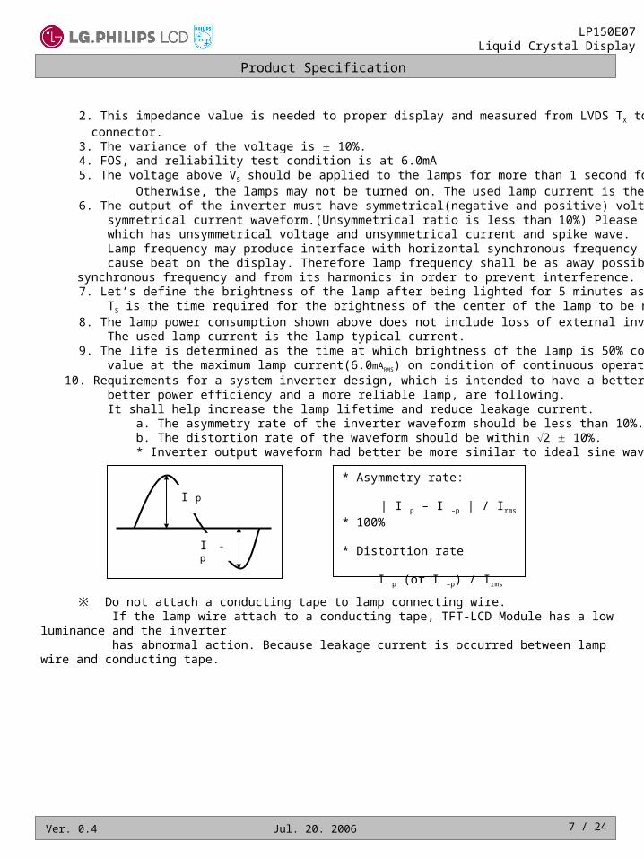
2. This impedance value is needed to proper display and measured from LVDS TX to the mating connector. 3. The variance of the voltage is 10%. 4. FOS, and reliability test condition is at 6.0mA 5. The voltage above VS should be applied to the lamps for more than 1 second for start-up. Otherwise, the lamps may not be turned on. The used lamp current is the lamp typical current. 6. The output of the inverter must have symmetrical(negative and positive) voltage waveform and symmetrical current waveform.(Unsymmetrical ratio is less than 10%) Please do not use the inverter which has unsymmetrical voltage and unsymmetrical current and spike wave. Lamp frequency may produce interface with horizontal synchronous frequency and as a result this may cause beat on the display. Therefore lamp frequency shall be as away possible from the horizontal
synchronous frequency and from its harmonics in order to prevent interference. 7. Let’s define the brightness of the lamp after being lighted for 5 minutes as 100%. TS is the time required for the brightness of the center of the lamp to be not less than 95%. 8. The lamp power consumption shown above does not include loss of external inverter. The used lamp current is the lamp typical current. 9. The life is determined as the time at which brightness of the lamp is 50% compared to that of initial value at the maximum lamp current(6.0mARMS) on condition of continuous operating at 25 2C 10. Requirements for a system inverter design, which is intended to have a better display performance, a better power efficiency and a more reliable lamp, are following. It shall help increase the lamp lifetime and reduce leakage current. a. The asymmetry rate of the inverter waveform should be less than 10%. b. The distortion rate of the waveform should be within 2 10%. * Inverter output waveform had better be more similar to ideal sine wave.
※ Do not attach a conducting tape to lamp connecting wire. If the lamp wire attach to a conducting tape, TFT-LCD Module has a low luminance and the inverter has abnormal action. Because leakage current is occurred between lamp wire and conducting tape.
I p
I -p
* Asymmetry rate: | I p – I –p | / Irms * 100%
* Distortion rate
I p (or I –p) / Irms

Product Specification
8 / 24
LP150E07Liquid Crystal Display
Ver. 0.4 Jul. 20. 2006
3-2. Interface Connections
Table 3. MODULE CONNECTOR PIN CONFIGURATION (CN1)
NotesDescriptionSymbolPin
The interface connections are compatible with ISP (Industry Standard Panels) 15.0” Mounting and Top Level Interface Requirements (Version2, June,2000) defined by SPWG (Standard Panels Working Group). This LCD employs two interface connections, a 30 pin connector is used for the module electronics and the other connector is used for the integral backlight system.The electronics interface connector is a model GT101-30S-HR11 manufactured by LG Cable. The pin configuration for the connector is shown in the table below.
Note: All GND(ground) pins should be connected together and to GND which should also be connected to the LCD’s metal frame. All VCC (power input) pins should be connected together.
The backlight interface connector is a model BHSR-02VS-1, manufactured by JST or Compatible.The mating connector part number is SM02B-BHSS-1 or equivalent.
Table 4. BACKLIGHT CONNECTOR PIN CONFIGURATION (J1)
Notes : 1. The high voltage side terminal is colored pink and the low voltage side terminal is Green.
Pin Symbol Description Notes
1 HV Power supply for lamp (High voltage side) 1
2 LV Power supply for lamp (Low voltage side) 1
130+LVDS differential clock(odd pixels)18
Ground19
-LVDS differential data (even pixels R0-R5, G0)20
Power Supply, 3.3V Typ.VCC2
Power Supply, 3.3V Typ.VCC3
for VEDIDVEDID4
For supplier test pointNC5
for ClkEDIDClkEDID6
for DataEDIDDATAEDID7
-LVDS differential data (odd pixels R0-R5, G0)Odd_RIN0-8
+LVDS differential data (odd pixels R0-R5, G0 )9
GroundVSS10
-LVDS differential data (odd pixels G1-G5, B0-B1 )11
+LVDS differential data (odd pixels G1-G5, B0-B1 )12
GroundVSS13
-LVDS differential data (odd pixels B2-B5, HS, VS, DE)14
+LVDS differential data (odd pixels B2-B5, HS, VS, DE)15
GroundVSS16
-LVDS differential clock (odd pixels)17
VSS Ground1
Ground28
-LVDS differential clock (even pixels)29
+LVDS differential clock (even pixels)30
+LVDS differential data (even pixels R0-R5, G0 )21
Ground22
-LVDS differential data (even pixels G1-G5, B0-B1 )23
+LVDS differential data (even pixels G1-G5, B0-B1 )24
Ground25
-LVDS differential data (even pixels B2-B5, HS, VS, DE)26
+LVDS differential data (even pixels B2-B5, HS, VS, DE)27
Odd_RIN0+
Odd_RIN1-
Odd_RIN1+
Odd_RIN2-
Odd_RIN2+
Odd_ClkIN-
Odd_ClkIN+
Even_RIN0-
VSS
VSS
VSS
Even_RIN0+
Even_RIN1-
Even_RIN1+
Even_RIN2-
Even_RIN2+
Even_ClkIN-
VSS
Even_ClkIN+
1, Interface chips 1.1 LCD : KZ4E064R11(LCD Controller) including LVDS Receiver 1.2 System : THC63LVDF823A or equivalent * Pin to Pin compatible with TI LVDS
2. Connector 2.1 LCD : FI-XB30SR-HF11, JAE or equivalent. 2.2 Mating : FI-X30M or equivalent. 2.3 Connector pin arrangement

Product Specification
9 / 24
LP150E07Liquid Crystal Display
Ver. 0.4 Jul. 20. 2006
3-3. Signal Timing Specifications
Table 5. Timing Table
ITEM SYMBOL MIN TYP MAX UNIT NOTES
Dclk Frequency - 36 54 54.5 MHz
HsyncPeriod tHP 732 800 848
tCLKWidth tWH 8 - -
Vsync
Period tVP 1060 1125 1150 tHP
Frequency fV 40 60
Width tWV 2 - -
Hz
tHP
DE(Data
Enable)
Horizontal Valid tHV 700 700 700
tCLK
Horizontal Back Porch tHBP 8 - -
Horizontal Front Porch tHFP 8 - -
Vertical Valid tVV
Vertical Back Porch tVBP
Vertical Front Porch tVFP
1050 1050 1050
tHP3 - -
1 - -
This is the signal timing required at the input of the User connector. All of the interface signal timing should be satisfied with the following specifications and specifications of LVDS Tx/Rx for it’s proper operation.
tHP
tHBP tHV tHFP
tVP
tWV
tVBP tVV tVFP
HSync
VSync
DE(Data Enable)
DE(Data Enable)
tWH
tCLK0.5 VccDCLK
3-4. Signal Timing Waveforms
High : 0.7Vcc
Low : 0.3Vcc
Hsync, Vsync, DE, Data
1)
1) 60 at Normal mode, 50,40 at Power save mode. Don’t care Flicker level.

Product Specification
10 / 24
LP150E07Liquid Crystal Display
Ver. 0.4 Jul. 20. 2006
3-5. Color Input Data Reference
The brightness of each primary color (red,green and blue) is based on the 6-bit gray scale data input for thecolor ; the higher the binary input, the brighter the color. The table below provides a reference for color versus data input.
Table 7. COLOR DATA REFERENCE
Color
Input Color Data
RED
MSB LSB
GREEN
MSB LSB
BLUE
MSB LSB
R5 R4 R3 R2 R1 R0 G5 G4 G3 G2 G1 G0 B5 B4 B3 B2 B1 B0
Basic
Color
Black 0 0 0 0 0 0 0 0 0 0 0 0 0 0 0 0 0 0
Red 1 1 1 1 1 1 0 0 0 0 0 0 0 0 0 0 0 0
Green 0 0 0 0 0 0 1 1 1 1 1 1 0 0 0 0 0 0
Blue 0 0 0 0 0 0 0 0 0 0 0 0 1 1 1 1 1 1
Cyan 0 0 0 0 0 0 1 1 1 1 1 1 1 1 1 1 1 1
Magenta 1 1 1 1 1 1 0 0 0 0 0 0 1 1 1 1 1 1
Yellow 1 1 1 1 1 1 1 1 1 1 1 1 0 0 0 0 0 0
White 1 1 1 1 1 1 1 1 1 1 1 1 1 1 1 1 1 1
RED
RED (00) 0 0 0 0 0 0 0 0 0 0 0 0 0 0 0 0 0 0
RED (01) 0 0 0 0 0 1 0 0 0 0 0 0 0 0 0 0 0 0
… … … …
RED (62) 1 1 1 1 1 0 0 0 0 0 0 0 0 0 0 0 0 0
RED (63) 1 1 1 1 1 1 0 0 0 0 0 0 0 0 0 0 0 0
GREEN
GREEN (00) 0 0 0 0 0 0 0 0 0 0 0 0 0 0 0 0 0 0
GREEN (01) 0 0 0 0 0 0 0 0 0 0 0 1 0 0 0 0 0 0
... … … …
GREEN (62) 0 0 0 0 0 0 1 1 1 1 1 0 0 0 0 0 0 0
GREEN (63) 0 0 0 0 0 0 1 1 1 1 1 1 0 0 0 0 0 0
BLUE
BLUE (00) 0 0 0 0 0 0 0 0 0 0 0 0 0 0 0 0 0 0
BLUE (01) 0 0 0 0 0 0 0 0 0 0 0 0 0 0 0 0 0 1
… … … …
BLUE (62) 0 0 0 0 0 0 0 0 0 0 0 0 1 1 1 1 1 0
BLUE (63) 0 0 0 0 0 0 0 0 0 0 0 0 1 1 1 1 1 1
Product Specification
11 / 24
LP150E07Liquid Crystal Display
Ver. 0.4 Jul. 20. 2006
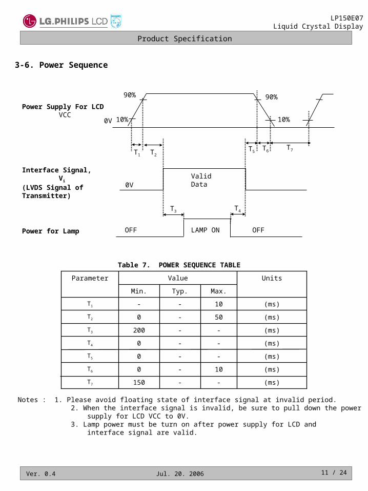
3-6. Power Sequence
T6
Interface Signal, Vi
(LVDS Signal of Transmitter)
Power for Lamp
Power Supply For LCD VCC
90%
10%10%0V
90%
T1 T2T5
Valid Data0V
OFFOFF LAMP ON
T7
T3 T4
Notes : 1. Please avoid floating state of interface signal at invalid period. 2. When the interface signal is invalid, be sure to pull down the power supply for LCD VCC to 0V. 3. Lamp power must be turn on after power supply for LCD and interface signal are valid.
(ms)--150T7
(ms)10-0T6
(ms)--0T5
(ms)--0T4
(ms)--200T3
(ms)50-0T2
(ms)10--T1
Max.Typ.Min.
UnitsValueParameter
Table 7. POWER SEQUENCE TABLE

Product Specification
12 / 24
LP150E07Liquid Crystal Display
Ver. 0.4 Jul. 20. 2006
4. Optical Specification
FIG. 1 Optical Characteristic Measurement Equipment and Method
Table 9. OPTICAL CHARACTERISTICS
Ta=25C, VCC=3.3V, fV=60Hz,Iout = 6.0mA
Parameter SymbolValues
Units NotesMin Typ MAx
Contrast Ratio CR 200 300 - 1
Surface Luminance, white LWH (at 6.0mA) 170 200 - cd/m2 2
Luminance Variation WHITE - - 55 % 3
Response Time Tr(TrR+ TrD) - 30 45 ms 4
Color Coordinates
RED RX 0.558 0.588 0.618
RY 0.313 0.343 0.373
GREEN GX 0.290 0.320 0.350
GY 0.510 0.540 0.570
BLUE BX 0.125 0.155 0.185
BY 0.110 0.140 0.170
WHITE WX 0.285 0.313 0.341
WY 0.309 0.329 0.349
Viewing Angle 5
x axis, right(=0) r 40 45 - degree
x axis, left (=180) l 40 45 - degree
y axis, up (=90) u 10 20 - degree
y axis, down (=270) d 30 40 - degree
Color Gamut 45 - %
LCD ModuleOptical Stage(x,y)
Pritchard 880 orequivalent
50cm
Optical characteristics are determined after the unit has been ‘ON’ and stable for approximately 30 minutes in a dark environment at 25C. The values specified are at an approximate distance 50cm from the LCD surface at a viewing angle of and equal to 0.FIG. 1 presents additional information concerning the measurement equipment and method.
Product Specification
13 / 24
LP150E07Liquid Crystal Display
Ver. 0.4 Jul. 20. 2006
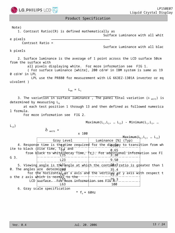
Note) 1. Contrast Ratio(CR) is defined mathematically as Surface Luminance with all white pixels Contrast Ratio = Surface Luminance with all black pixels
2. Surface luminance is the average of 1 point across the LCD surface 50cm from the surface with all pixels displaying white. For more information see FIG 1. ( For surface Luminance [white], 200 cd/m2 in IBM system is same as 190 cd/m2 in LPL LPL use the PR880 for measurement with LG 663EZ-1301A inverter or equivalent )
LWH = L1
3. The variation in surface luminance , The panel total variation ( WHITE) is determined by measuring LN
at each test position 1 through 13 and then defined as followed numerical formula. For more information see FIG 2.
Maximum(L1,L2, … L13) - Minimum(L1,L2, … L13) WHITE = x 100 Maximum(L1,L2, … L13)
4. Response time is the time required for the display to transition from white to black (rise time, TrR) and from black to white(Decay Time, TrD). For additional information see FIG 3.
5. Viewing angle is the angle at which the contrast ratio is greater than 10. The angles are determined for the horizontal or x axis and the vertical or y axis with respect to the z axis which is normal to the LCD surface. For more information see FIG 4.
6. Gray scale specification * fV = 60HzGray Level Luminance [%] (Typ)
L0 0.20
L7 0.65
L15 3.30
L23 9.50
L31 20.3
L39 35.4
L47 53.0
L55 79.3
L63 100

Product Specification
14 / 24
LP150E07Liquid Crystal Display
Ver. 0.4 Jul. 20. 2006
FIG. 3 Response Time
The response time is defined as the following figure and shall be measured by switching the input signal for “black” and “white”.
TrR TrD
100
90
100
%
Optical
Response
whiteblack
white
FIG. 2 Luminance
<measuring point for surface luminance & measuring point for luminance variation>
H
A
V
B
L4 L5
L1
L2 L3
Center Point
D
C H,V : ACTIVE AREAA : H/4 mmB : V/4 mmC : 10 mmD : 10 mmPOINTS : 13 POINTS
L12
L7
L9 L10
L6
L11 L13
L8

Product Specification
15 / 24
LP150E07Liquid Crystal Display
Ver. 0.4 Jul. 20. 2006
FIG. 4 Viewing angle
<Dimension of viewing angle range>
Normal
YEye
= 0 ,Right
= 180 ,Left
= 270 ,Down
= 90 , Up
Product Specification
16 / 24
LP150E07Liquid Crystal Display
Ver. 0.4 Jul. 20. 2006
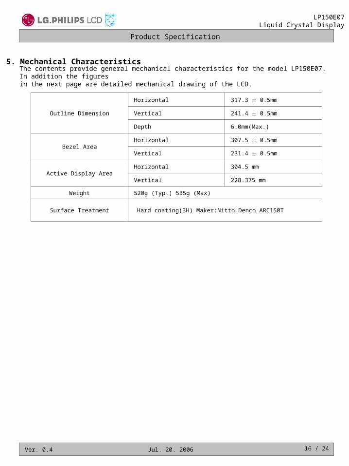
5. Mechanical CharacteristicsThe contents provide general mechanical characteristics for the model LP150E07. In addition the figuresin the next page are detailed mechanical drawing of the LCD.
Outline Dimension
Horizontal 317.3 0.5mm
Vertical 241.4 0.5mm
Depth 6.0mm(Max.)
Bezel AreaHorizontal 307.5 0.5mm
Vertical 231.4 0.5mm
Active Display AreaHorizontal 304.5 mm
Vertical 228.375 mm
Weight 520g (Typ.) 535g (Max)
Surface Treatment Hard coating(3H) Maker:Nitto Denco ARC150T

Product Specification
17 / 24
LP150E07Liquid Crystal Display
Ver. 0.4 Jul. 20. 2006
<FRONT VIEW> Note) Unit:[mm], General tolerance: 0.5mm

Product Specification
18 / 24
LP150E07Liquid Crystal Display
Ver. 0.4 Jul. 20. 2006
<REAR VIEW> Note) Unit:[mm], General tolerance: 0.5mm

Product Specification
19 / 24
LP150E07Liquid Crystal Display
Ver. 0.4 Jul. 20. 2006
[ DETAIL DESCRIPTION OF SIDE MOUNTING SCREW ]
* Screw Torque : 2.5kgf.cm Max* Screw Hole Depth (“A”) : Max 2.5mm* Screw Penetration Length (“B”) : Max 2.5, Min 2.3

Product Specification
20 / 24
LP150E07Liquid Crystal Display
Ver. 0.4 Jul. 20. 2006
6. Reliability
Environment test condition
{ Result Evaluation Criteria } There should be no change which might affect the practical display function when the display qualitytest is conducted under normal operating condition.
No. Test Item Conditions
1 High temperature storage test Ta= 60C, 240h
2 Low temperature storage test Ta= -20C, 240h
3 High temperature operation test Ta= 50C, 50%RH, 240h
4 Low temperature operation test Ta= 0C, 240h
5 Vibration test (non-operating) Sine wave, 10 ~ 500 ~ 10Hz, 1.5G, 0.37oct/min3 axis, 1hour/axis
6 Shock test (non-operating) Half sine wave, 180G, 2msone shock of each six faces(I.e. run 180G 2msfor all six faces)
7 Altitude operating storage / shipment
0 ~ 10,000 feet (3,048m) 24Hr0 ~ 40,000 feet (12,192m) 24Hr

Product Specification
21 / 24
LP150E07Liquid Crystal Display
Ver. 0.4 Jul. 20. 2006
7. International Standards
7-1. Safety
a) UL 60950, Third Edition, Underwriters Laboratories, Inc., Dated Dec. 11, 2000. Standard for Safety of Information Technology Equipment, Including Electrical Business Equipment.
b) CAN/CSA C22.2, No. 60950, Third Edition, Canadian Standards Association, Dec. 1, 2000. Standard for Safety of Information Technology Equipment, Including Electrical Business Equipment.
c) EN 60950 : 2000, Third Edition IEC 60950 : 1999, Third Edition European Committee for Electrotechnical Standardization(CENELEC) EUROPEAN STANDARD for Safety of Information Technology Equipment Including Electrical Business Equipment.
7-2. EMC
a) ANSI C63.4 “Methods of Measurement of Radio-Noise Emissions from Low-Voltage Electrical and Electrical Equipment in the Range of 9kHZ to 40GHz. “American National Standards Institute(ANSI),
1992b) C.I.S.P.R “Limits and Methods of Measurement of Radio Interface Characteristics of Information
Technology Equipment.“ International Special Committee on Radio Interference.c) EN 55022 “Limits and Methods of Measurement of Radio Interface Characteristics of Information
Technology Equipment.“ European Committee for Electrotechnical Standardization.(CENELEC), 1998 ( Including A1: 2000 )
Product Specification
22 / 24
LP150E07Liquid Crystal Display
Ver. 0.4 Jul. 20. 2006
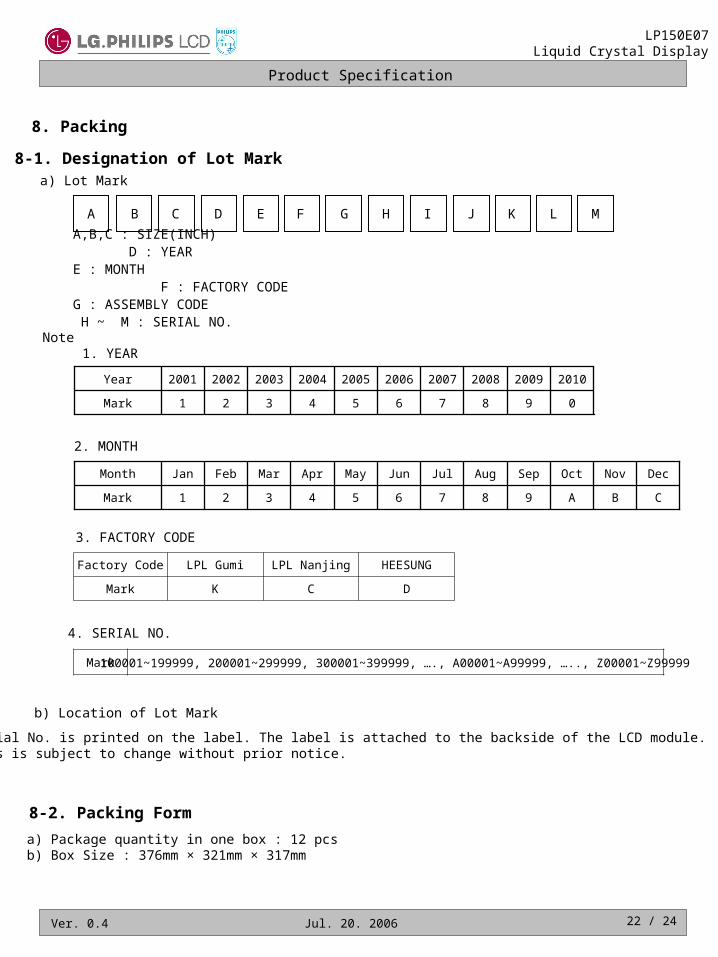
8. Packing
8-2. Packing Form
a) Package quantity in one box : 12 pcsb) Box Size : 376mm × 321mm × 317mm
8-1. Designation of Lot Marka) Lot Mark
A B C D E F G H I J K L M
A,B,C : SIZE(INCH) D : YEAR E : MONTH F : FACTORY CODE G : ASSEMBLY CODE H ~ M : SERIAL NO.
Note 1. YEAR
2. MONTH
4. SERIAL NO.
Mark
Year
0
2010
6
2006
7
2007
8
2008
9
2009
4
2004
5
2005
321
200320022001
B
Nov
Mark
Month
A
Oct
6
Jun
7
Jul
8
Aug
9
Sep
4
Apr
5
May
C321
DecMarFebJan
3. FACTORY CODE
Factory Code LPL Gumi LPL Nanjing HEESUNG
Mark K C D
b) Location of Lot Mark
Serial No. is printed on the label. The label is attached to the backside of the LCD module.This is subject to change without prior notice.
Mark 100001~199999, 200001~299999, 300001~399999, …., A00001~A99999, ….., Z00001~Z99999
Product Specification
23 / 24
LP150E07Liquid Crystal Display
Ver. 0.4 Jul. 20. 2006
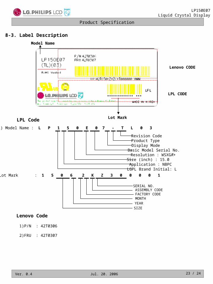
8-3. Label Description
Model Name
LPL Code
1)P/N : 42T0306
2)FRU : 42T0307
Lenovo Code
(1) Model Name : L P 1 5 0 E 0 7 - T L 0 3
Revision CodeProduct TypeDisplay ModeBasic Model Serial No.Resolution : WSXGA+Size (inch) : 15.0”Application : NBPCLGPL Brand Initial: L
Lot Mark
(2) Lot Mark : 1 5 0 6 2 K Z 3 0 0 0 0 1
SERIAL NO.ASSEMBLY CODE
MONTHYEARSIZE
FACTORY CODE
LPL CODE
Lenovo CODE

Product Specification
24 / 24
LP150E07Liquid Crystal Display
Ver. 0.4 Jul. 20. 2006
9. PRECAUTIONS
Please pay attention to the followings when you use this TFT LCD module.
9-1. MOUNTING PRECAUTIONS
(1) You must mount a module using holes arranged in four corners or four sides.(2) You should consider the mounting structure so that uneven force (ex. Twisted stress) is not applied to the module. And the case on which a module is mounted should have sufficient strength so that external
force is not transmitted directly to the module.(3) Please attach the surface transparent protective plate to the surface in order to protect the polarizer. Transparent protective plate should have sufficient strength in order to the resist external force.(4) You should adopt radiation structure to satisfy the temperature specification.(5) Acetic acid type and chlorine type materials for the cover case are not desirable because the former generates corrosive gas of attacking the polarizer at high temperature and the latter causes circuit break
by electro-chemical reaction.(6) Do not touch, push or rub the exposed polarizers with glass, tweezers or anything harder than HB pencil lead. And please do not rub with dust clothes with chemical treatment. Do not touch the surface of polarizer for bare hand or greasy cloth.(Some cosmetics are detrimental to the polarizer.)(7) When the surface becomes dusty, please wipe gently with absorbent cotton or other soft materials like
chamois soaks with petroleum benzene. Normal-hexane is recommended for cleaning the adhesives used to attach front / rear polarizers. Do not use acetone, toluene and alcohol because they cause chemical damage to the polarizer.
(8) Wipe off saliva or water drops as soon as possible. Their long time contact with polarizer causes deformations and color fading.
(9) Do not open the case because inside circuits do not have sufficient strength.
9-2. OPERATING PRECAUTIONS
(1) The spike noise causes the mis-operation of circuits. It should be lower than following voltage : V=± 200mV(Over and under shoot voltage)
(2) Response time depends on the temperature.(In lower temperature, it becomes longer.)(3) Brightness depends on the temperature. (In lower temperature, it becomes lower.) And in lower temperature, response time(required time that brightness is stable after turned on) becomes longer.(4) Be careful for condensation at sudden temperature change. Condensation makes damage to polarizer or
electrical contacted parts. And after fading condensation, smear or spot will occur.(5) When fixed patterns are displayed for a long time, remnant image is likely to occur.(6) Module has high frequency circuits. Sufficient suppression to the electromagnetic interference shall be
done by system manufacturers. Grounding and shielding methods may be important to minimized the interference.

Product Specification
25 / 24
LP150E07Liquid Crystal Display
Ver. 0.4 Jul. 20. 2006
Since a module is composed of electronic circuits, it is not strong to electrostatic discharge. Make certain that treatment persons are connected to ground through wrist band etc. And don’t touch interface pin directly.
9-3. ELECTROSTATIC DISCHARGE CONTROL
Strong light exposure causes degradation of polarizer and color filter.
9-4. PRECAUTIONS FOR STRONG LIGHT EXPOSURE
9-5. STORAGE
(1) The protection film is attached to the bezel with a small masking tape. When the protection film is peeled off, static electricity is generated between the film and polarizer. This should be peeled off slowly and carefully by people who are electrically grounded and with well ion-blown equipment or in such a condition, etc.(2) When the module with protection film attached is stored for a long time, sometimes there remains a very small amount of glue still on the bezel after the protection film is peeled off.(3) You can remove the glue easily. When the glue remains on the bezel surface or its vestige is recognized, please wipe them off with absorbent cotton waste or other soft material like chamois soaked with normal-hexane.
9-6. HANDLING PRECAUTIONS FOR PROTECTION FILM
When storing modules as spares for a long time, the following precautions are necessary.
(1) Store them in a dark place. Do not expose the module to sunlight or fluorescent light. Keep the temperature between 5C and 35C at normal humidity.
(2) The polarizer surface should not come in contact with any other object. It is recommended that they be stored in the container in which they were shipped.
Product Specification
26 / 24
LP150E07Liquid Crystal Display
Ver. 0.4 Jul. 20. 2006
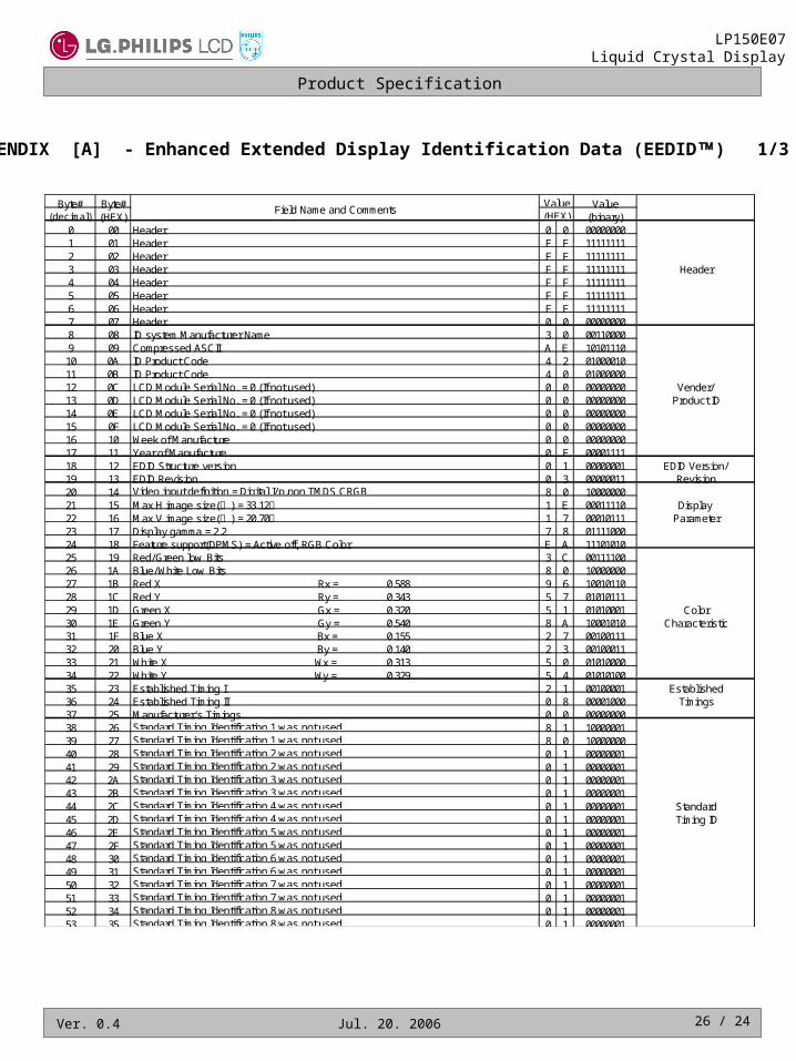
APPENDIX [A] - Enhanced Extended Display Identification Data (EEDID) 1/3
Byte# Byte# Value(decimal) (HEX) (binary)
0 00 Header 0 0 000000001 01 Header F F 111111112 02 Header F F 111111113 03 Header F F 11111111 Header4 04 Header F F 111111115 05 Header F F 111111116 06 Header F F 111111117 07 Header 0 0 000000008 08 ID system Manufacturer Name 3 0 001100009 09 Compressed ASCII A E 1010111010 0A ID Product Code 4 2 0100001011 0B ID Product Code 4 0 0100000012 0C LCD Module Serial No. = 0 (If not used) 0 0 00000000 Vender/13 0D LCD Module Serial No. = 0 (If not used) 0 0 00000000 Product ID14 0E LCD Module Serial No. = 0 (If not used) 0 0 0000000015 0F LCD Module Serial No. = 0 (If not used) 0 0 0000000016 10 Week of Manufacture 0 0 0000000017 11 Year of Manufacture 0 F 0000111118 12 EDID Structure version 0 1 00000001 EDID Version/19 13 EDID Revision 0 3 00000011 Revision20 14 8 0 1000000021 15 Max H image size( ) = 33.12㎝ ㎝ 1 E 00011110 Display 22 16 Max V image size( ) = 20.70㎝ ㎝ 1 7 00010111 Parameter23 17 Display gamma = 2.2 7 8 0111100024 18 Feature support(DPMS) = Active off, RGB Color E A 1110101025 19 Red/Green low Bits 3 C 0011110026 1A Blue/White Low Bits 8 0 1000000027 1B Red X Rx = 0.588 9 6 1001011028 1C Red Y Ry = 0.343 5 7 0101011129 1D Green X Gx = 0.320 5 1 01010001 Color30 1E Green Y Gy = 0.540 8 A 10001010 Characteristic31 1F Blue X Bx = 0.155 2 7 0010011132 20 Blue Y By = 0.140 2 3 0010001133 21 White X Wx = 0.313 5 0 0101000034 22 White Y Wy = 0.329 5 4 0101010035 23 Established Timing I 2 1 00100001 Established36 24 Established Timing II 0 8 00001000 Timings37 25 Manufacturer's Timings 0 0 0000000038 26 8 1 1000000139 27 8 0 1000000040 28 0 1 0000000141 29 0 1 0000000142 2A 0 1 0000000143 2B 0 1 0000000144 2C 0 1 00000001 Standard45 2D 0 1 00000001 Timing ID46 2E 0 1 0000000147 2F 0 1 0000000148 30 0 1 0000000149 31 0 1 0000000150 32 0 1 0000000151 33 0 1 0000000152 34 0 1 0000000153 35 0 1 00000001
Standard Timing Identification 4 was not used
Standard Timing Identification 6 was not used
Standard Timing Identification 8 was not usedStandard Timing Identification 8 was not used
Standard Timing Identification 5 was not used
Standard Timing Identification 7 was not used
Standard Timing Identification 3 was not usedStandard Timing Identification 3 was not used
Standard Timing Identification 1 was not usedStandard Timing Identification 1 was not usedStandard Timing Identification 2 was not usedStandard Timing Identification 2 was not used
Value(HEX)
Field Name and Comments
Video input definition = Digital I/p,non TMDS CRGB
Standard Timing Identification 4 was not used
Standard Timing Identification 7 was not used
Standard Timing Identification 6 was not usedStandard Timing Identification 5 was not used

Product Specification
27 / 24
LP150E07Liquid Crystal Display
Ver. 0.4 Jul. 20. 2006
Byte# Byte# Value(decimal) (HEX) (binary)
54 36 Pixel Clock/10,000 (LSB) 3 0 0011000055 37 Pixel Clock/10,000 (MSB) / 2 A 0010101056 38 Horizontal Active 7 8 0111100057 39 Horizontal Blanking 2 0 0010000058 3A Horizontal Active : Horizontal Blanking 5 1 0101000159 3B Vertical Avtive 1 A 0001101060 3C Vertical Blanking 1 0 00010000 Detailed61 3D Vertical Active : Vertical Blanking 4 0 01000000 Timing62 3E Horizontal Sync. Offset 3 0 00110000 Description63 3F Horizontal Sync Pulse Width 7 0 01110000 #164 40 Vertical Sync Offset : Sync Width 1 3 0001001165 41 Horizontal Vertical Sync Offset/Width upper 2bits = 0 0 0 0000000066 42 Horizontal Image Size 3 0 0011000067 43 Vertical Image Size E 4 1110010068 44 Horizontal & Vertical Image Size 1 0 0001000069 45 Horizontal Border = 0 0 0 0000000070 46 Vertical Border = 0 0 0 0000000071 47 Non- interlaced,Normal display,no stereo,Digital separate sync,H/V pol negatives 1 8 0001100072 48 Pixel Clock/10,000 (LSB) 50Hz 2 5 0010010173 49 Pixel Clock/10,000 (MSB) / 50Hz 2 3 0010001174 4A Horizontal Active 7 8 0111100075 4B Horizontal Blanking 2 0 0010000076 4C Horizontal Active : Horizontal Blanking 5 1 0101000177 4D Vertical Avtive 1 A 0001101078 4E Vertical Blanking 1 0 00010000 Detailed79 4F Vertical Active : Vertical Blanking 4 0 01000000 Timing80 50 Horizontal Sync. Offset 3 0 00110000 Description81 51 Horizontal Sync Pulse Width 7 0 01110000 #282 52 Vertical Sync Offset : Sync Width 1 3 0001001183 53 Horizontal Vertical Sync Offset/Width upper 2bits = 0 0 0 0000000084 55 Horizontal Image Size 3 0 0011000085 55 Vertical Image Size E 4 1110010086 56 Horizontal & Vertical Image Size 1 0 0001000087 57 Horizontal Border = 0 0 0 0000000088 58 Vertical Border = 0 0 0 0000000089 59 Non-interlaced,Normal display,no stereo,Digital separate sync,H/V pol negatives 1 8 0001100090 5A Detailed Timing Descriptor #3 0 0 0000000091 5B 0 0 0000000092 5C 0 0 0000000093 5D 0 F 0000111194 5E 0 0 0000000095 5F (Horizontal active pixel /8)-31 9 0 1001000096 60 Image Aspect Ratio(16:10) 4 3 01000011 Detailed97 61 Low Refresh Rate #1(50Hz) 3 2 00110010 Timing98 62 (Horizontal active pixel /8)-31 9 0 10010000 Description99 63 Image Aspect Ratio(16:10) 4 3 01000011 #3100 64 Low Refresh Rate #2(40Hz) 2 8 00101000101 65 Brightness(1/10nit) 1 4 00010100102 66 Feature flag(TN mode) 0 1 00000001103 67 Reserved 00h 0 0 00000000104 68 EISA manufacturer code(3 Character ID) 3 2 00110010105 69 Compressed ASCII 0 C 00001100106 6A Panel Supplier Reserved - Product code 5 3 01010011107 6B (Hex, LSB first) 2 1 00100001
ASCII Data String Tag (Supplier Name)
Field Name and Comments(HEX)Value
APPENDIX [A] - Enhanced Extended Display Identification Data (EEDID) 2/3

Product Specification
28 / 24
LP150E07Liquid Crystal Display
Ver. 0.4 Jul. 20. 2006
APPENDIX [A] - Enhanced Extended Display Identification Data (EEDID) 3/3
Byte# Byte# Value(decimal) (HEX) (binary)
108 6C Detailed Timing Descriptor #4 0 0 00000000109 6D 0 0 00000000110 6E 0 0 00000000111 6F F E 11111110112 70 0 0 00000000113 71 L 4 C 01001100114 72 P 5 0 01010000 Detailed115 73 1 3 1 00110001 Timing116 74 5 3 5 00110101 Description117 75 0 3 0 00110000 #4118 76 E 4 5 01000101119 77 0 3 0 00110000120 78 7 3 7 00110111121 79 - 2 D 00101101122 7A T 5 4 01010100123 7B L 4 C 01001100124 7C 0 3 0 00110000125 7D 3 3 3 00110011126 7E Extension flag = 00 0 0 00000000 Extension Flag127 7F Checksum C A 11001010 Checksum
ASCII Data String Tag (Supplier S/N)
Field Name and Comments(HEX)Value