prof. j. raynien kwo department of physics national tsing...
TRANSCRIPT
Introduction to Nanophysics
Prof. J. Raynien Kwo
Department of Physics
National Tsing Hua University Feb. 21, 2013

1
One (nm) equals to 1/1000000000 (10-9) meter
What is the size for a “nano” ?
10-3 m , Macro
10-6 m , Micro
10-9 m , Meso

2
“ There’s plenty of
room at the bottom ! ”
in 1959.
R. Feymann Already Knew about this !
3
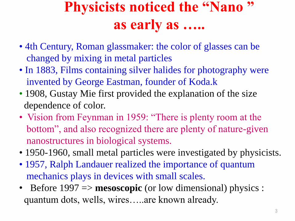
Physicists noticed the “Nano ”
as early as …..
• 4th Century, Roman glassmaker: the color of glasses can be
changed by mixing in metal particles • In 1883, Films containing silver halides for photography were
invented by George Eastman, founder of Koda.k
• 1908, Gustay Mie first provided the explanation of the size
dependence of color.
• Vision from Feynman in 1959: “There is plenty room at the
bottom”, and also recognized there are plenty of nature-given
nanostructures in biological systems.
• 1950-1960, small metal particles were investigated by physicists.
• 1957, Ralph Landauer realized the importance of quantum
mechanics plays in devices with small scales.
• Before 1997 => mesoscopic (or low dimensional) physics :
quantum dots, wells, wires…..are known already.

4
Nano
Materials
Nano
Science and
Technology
Nanoproducts
(Devices and
Systems)
Nano Processing
and
Characterization
Major Topics of Nanoscience and Technology

5
What is the Nano Technology?
Science and Technology Down scaling to size under100 nm: Via the “Top-down” lithographic pattering. -- Moore’s law !
Manipulate the atomic and molecular structures:“Bottom-up” nano materials, growth and assembly. Feymann: There’s plenty of room at the bottom

6
Major Driving Force pushing for Nano
Moore‘s Law : A 30% decrease in the size of
printed dimensions every two years.
Is due to the bottle neck met in Microelectronics


8
1960 Kahng and Atalla, First MOSFET
1970 First IC, 1 kbit, 750 khz microprocessor
Metal-Oxide-Feld Effect Transistor


11
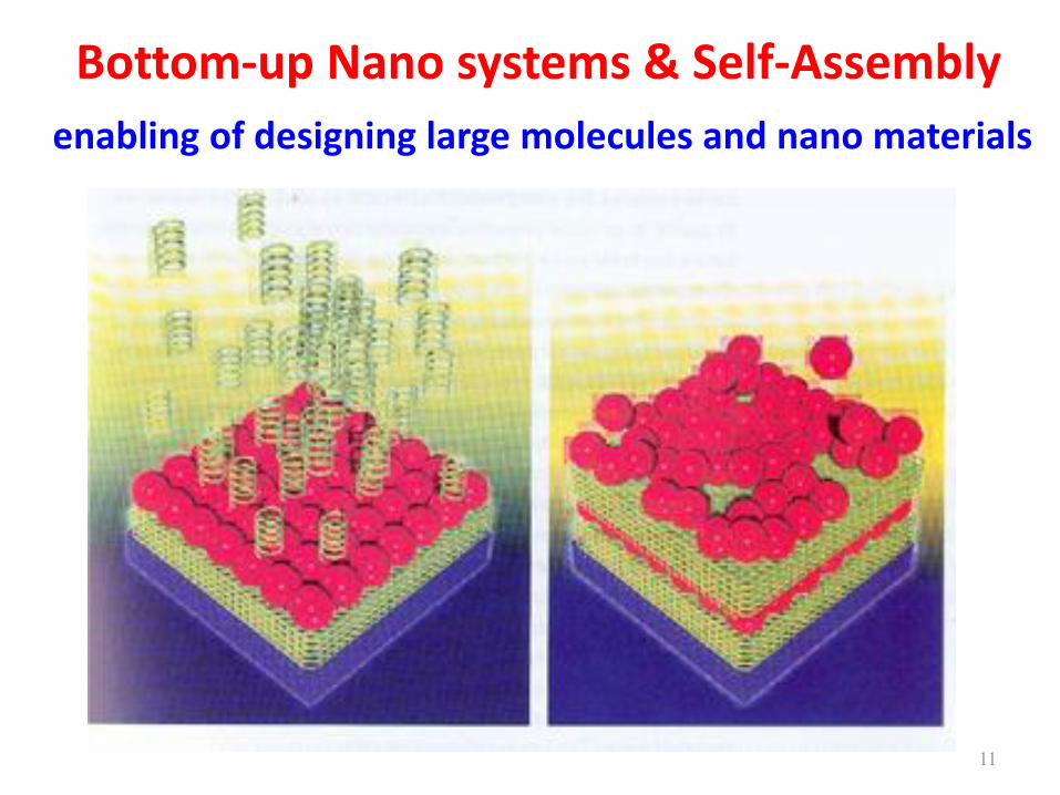
Bottom-up Nano systems & Self-Assembly
enabling of designing large molecules and nano materials

12
The First Lesson :
Bulk-to-nano Transition

13
Ex: size-dependence of melting temperature
Ph. Buffat and J-P. Borel, Phys. Rev. A13, 2287 (1976)
Ag

14
powered cadmium selenide
larger
smaller
Ex: size-dependence of color

15
Ex: size-dependence of magnetism
A. J. Cox et al. Phys. Rev. B49, 12295 (1994)

16
• The ability of growing the nano scale
materials and structures
• The ability of detecting and manipulating
on the nano scale.
The Second Lesson :

17
(I) Advance in thin film growth:
Such as Molecular Beam Epitaxy, atomic layer
depostion, laser MBE, etc…
For Nano electronics in metals, oxides, and
semiconductors
(II) Detection at nano scale : STM, AFM,
MFM, STEM, Cs-TEM
In 1982, Binning, and Rohrer in IBM invented
scanning tunneling microscope.
In 1986, Binning, Quate, and Gerber invented the
atomic force microscope AFM.

18
Now located in the Nano
Technology Center, ITRI,
Hsin Chu, Taiwan
For Metal, Oxide and
Semiconductor Films
On the Nano scale
Integrated MBE Multi-chamber System

19
Scanning Tunneling Microscope (STM)
20
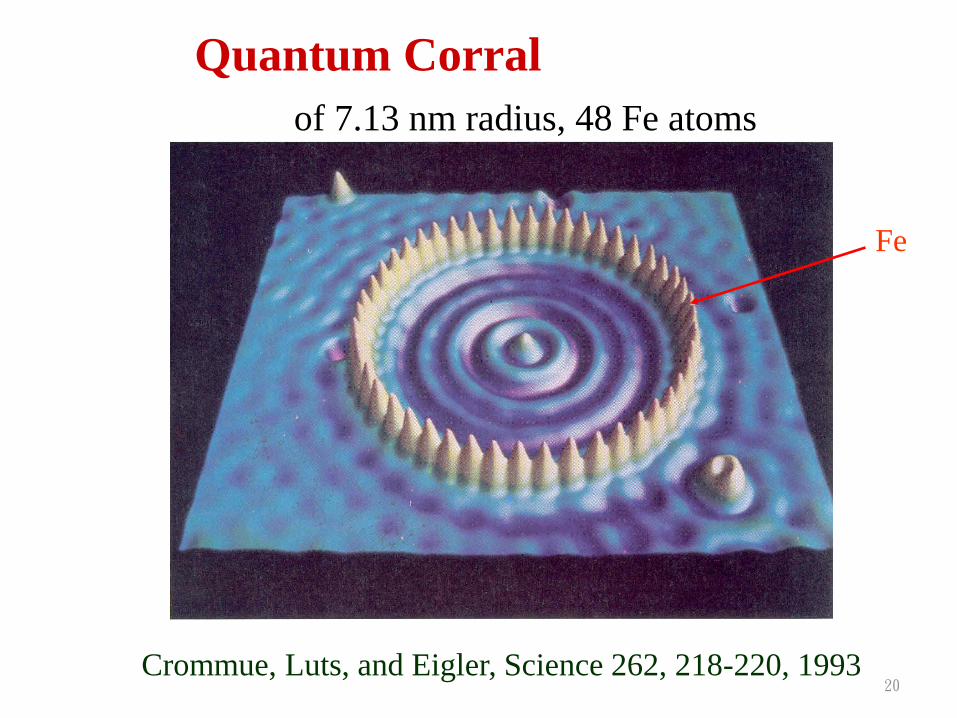
Quantum Corral
Crommue, Luts, and Eigler, Science 262, 218-220, 1993
Fe
of 7.13 nm radius, 48 Fe atoms

EDX
EELS
Cs
corrector
EELS
Electron
Mono-
chromator
Scanning Transmission Electron Microscope Laboratory
2-Å STEM 1-Å STEM
E~0.2 eV E~0.9 eV
Prof. C. H. Chen and
Dr. M.-W. Chu.

Spherical Aberration Corrected (球面相差)
Cs-STEM by C. H. Chen at CCMS, NTU
Cs
corrector
JEOL 2100;
2009四月底裝機完成
Cs
corrector
Cs
lens
Cs corrected
lens sample
sample
focus confusion!

High-Angle ADF: Si dumbbell, 1.36 Å spacing
15s exposure
Si [110]
60s exposure
Drift ~1Å /min !!
(004):
1.36Å
(440);
0.96Å
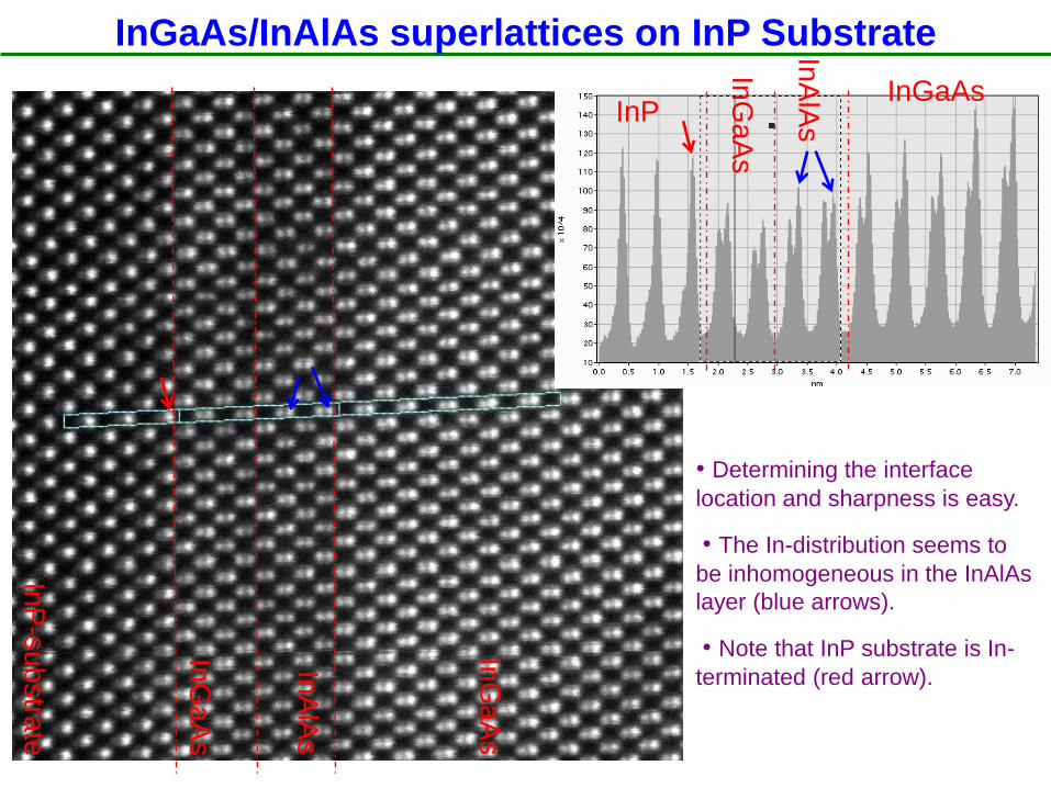
InP
-su
bstra
te
InG
aA
s
InA
lAs
InG
aA
s
• Determining the interface
location and sharpness is easy.
• The In-distribution seems to
be inhomogeneous in the InAlAs
layer (blue arrows).
• Note that InP substrate is In-
terminated (red arrow).
InGaAs/InAlAs superlattices on InP Substrate
InG
aA
s
InA
lAs
InGaAs InP

2-Å Electron Probe SrTiO3
Z-contrast
cubic; a = 3.905 Å
Sr Ti
O
Atomic Resolution STEM Imaging: Z-contrast
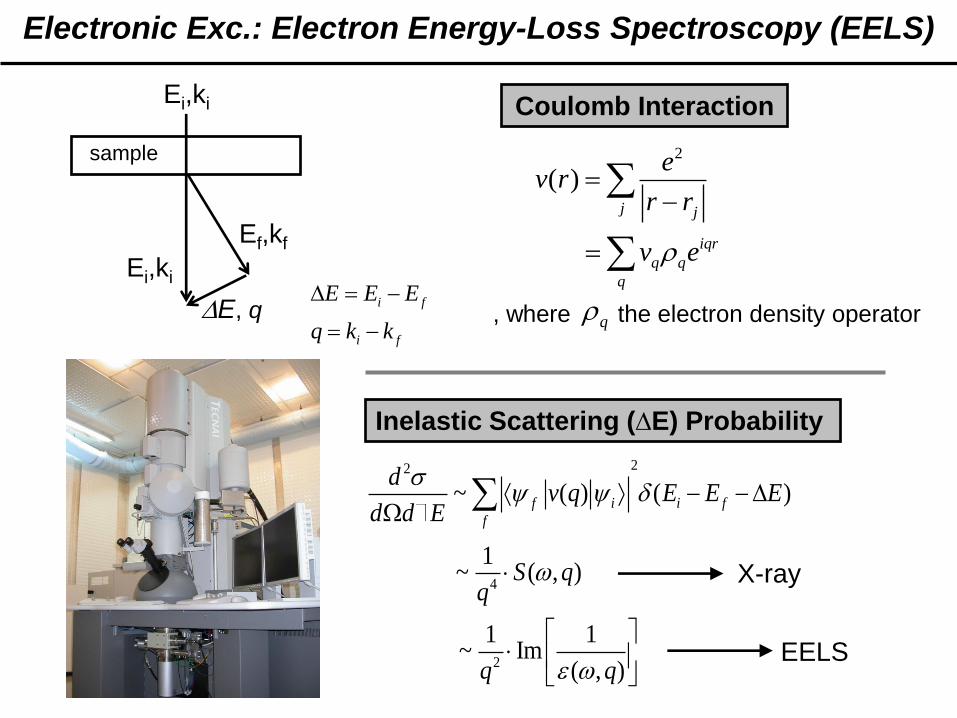
Electronic Exc.: Electron Energy-Loss Spectroscopy (EELS)
sample
Ei,ki
Ei,ki
E, q
Ef,kf
i f
i f
E E E
q k k
Coulomb Interaction
2
( )j j
ev r
r r
iqr
q q
q
v e
q, where the electron density operator
Inelastic Scattering (∆E) Probability
22
~ ( ) ( )f i i f
f
dv q E E E
d d E
4
1~ ( , )S q
q
2
1 1~ Im
( , )q q
X-ray
EELS

Spectral Imaging at Ultimate Spatial Resolution
27 nm
81 nm
8 nm
2.38 eV Bright Mode
1.82 eV Dark Mode
Au Au
Plasmonic Mapping:
STEM-EELS (2-Å Probe)
Chemical Mapping:
STEM-EDX (1-Å Probe)
1.47 Å
M.-W. Chu et al., Nano Lett. 9, 399 (2009). M.-W. Chu et al., Phys. Rev. Lett. 104, 196101 (2010).

28
The Third Lesson:
The importance of
Quantum Physics

29
The cause for variation of scaling
• Influence of Boundary --Increase of proportion of boundaries --Existence of surface / edge modes --Geometrical reconstruction
• Decrease of the number of particles decrease of confinement , increase of purturbation • Different scaling for different physical entity
Quantum Effect:
=> Most likely to have new breakthough !

The connection of materials wave
with mechanics
h = Planck constant (6.62610-34 joule-sec)
DeBroglie:
= h/p
Einstein:
E=h=p2/2m
(300 ) 6.2
(300 ) 0.
:
( 10 100
2
自由電子
半導體
原子:
中 )
th
th
nm
K
nm
K nm
nm
Wave length Free electrons
Semiconductors
Atoms

31
Bulk Limit Nano Limit
L
Bulk
materials
<< L
Nano ~ L
32
Major Qauntum Effect
at the nano scale
• Interference
• Quantization
• Tunneling
• Quantum Spin

33
(I) Interference

34
Classical mechanics
?
The wonder of electron in waves
Electron source

35
The wave property of electrons

36
Electron source
Double Slit Interference of Electrons
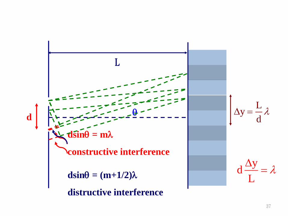
37
d
dsin = m
constructive interference
L
yd
L
Ly
d
dsin = (m+1/2)
distructive interference

38
Ly
d
7mm
1L m
1 410 10d mm m 700nm
y 1.7 m
~~
~
~ ~ ~ 0.17nm

39
(II) Quantization

40
Standing Wave
Confinement of the materials wave
Quantizations

41
The Qauntization of Energy
L
n
2L
n 1
n 2
n 3
2
h nhp
L
2 2
2
2
2 8 n
p n hE
mLm
21/ E L

42
Quantum well: 1D confinement
2D electron Gas
二維電子氣
AlGaAs
GaAs
FE
MOSFET:
e
AlGaAs
GaAs

43
Quantum wire: 2 D-Confinement
z
y
x
SEM images of MoOx nanowires on graphite surfaces Science 290, 2120-2123, (2000)
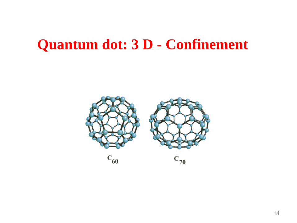
44
Quantum dot: 3 D - Confinement

45
Quantum Dots of various shape

46
powdered Cadmium Selenide
larger
smaller
0
2/ 1/ E hc L
Absorption in scattering From red to yellow
larger


The Advent of Carbon Era ?


50
Carbon Nanotube

51
Carbon Nanotube
Carbon Nanotube based Transistors / Electronics


Exfoliated Graphene
Monolayers and Bilayers
Monolayer Bilayer
Reflecting microscope images.
K. S. Novoselov et al., Science 306, 666 (2004).
20 m


Relativistic Dirac fermion.
Band Structure near K Points
~10 eV

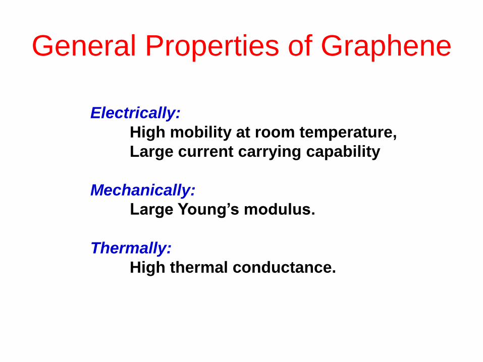
Electrically:
High mobility at room temperature,
Large current carrying capability
Mechanically:
Large Young’s modulus.
Thermally:
High thermal conductance.
General Properties of Graphene

-Quantum Hall effect
-Barry Phase
-Ballistic transport
-Klein’s paradox
-Others
.
.
Exotic Behaviors

Quantum Hall Effect
Y. Zhang et al, Nature 438, 201(2005)

As the potential approaches infinity, the reflection diminishes,
the electron always transmittes
(1929)
Electron scattering from a potential barrier
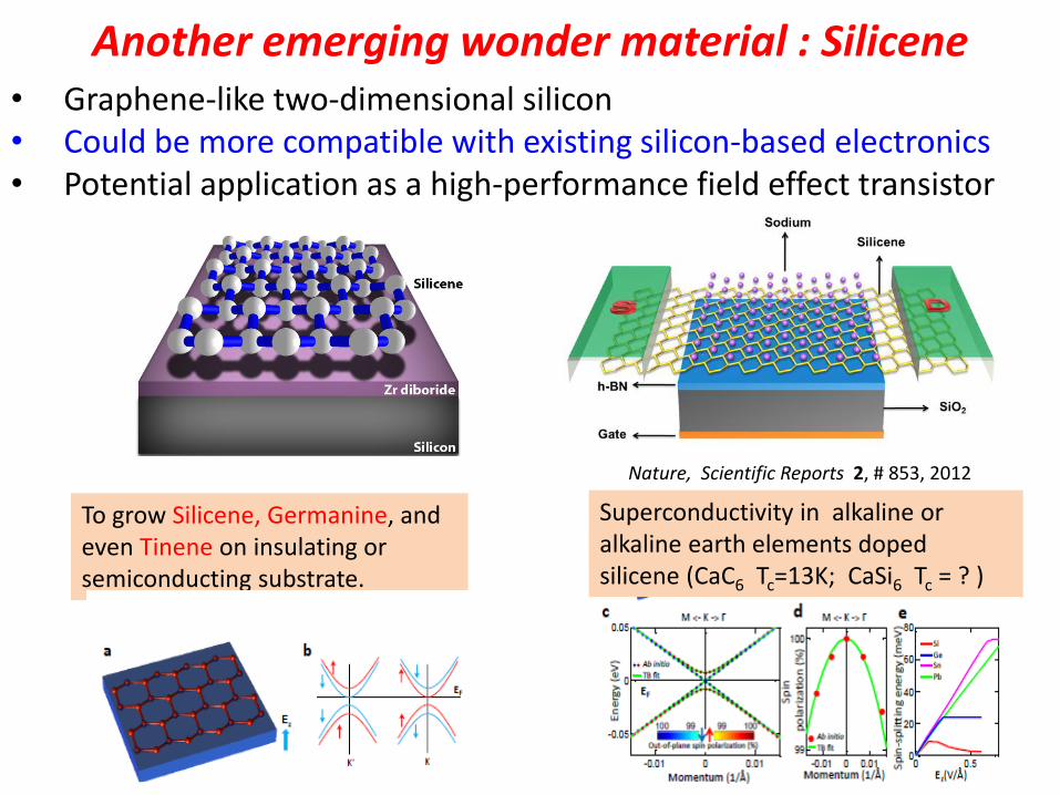
Another emerging wonder material : Silicene • Graphene-like two-dimensional silicon • Could be more compatible with existing silicon-based electronics • Potential application as a high-performance field effect transistor
Nature, Scientific Reports 2, # 853, 2012
To grow Silicene, Germanine, and even Tinene on insulating or semiconducting substrate.
Superconductivity in alkaline or alkaline earth elements doped silicene (CaC6 Tc=13K; CaSi6 Tc = ? )

Combined spectroscopic and microscopic study underway
Synchrotron radiation core level photoemission from NSRRC
Scanning Tunneling Microscopy
60s = 1 ML
67
(III) Tunneling

68
nm

69
Quantum Tunneling is the major effect
for the failure of Transistor at nano scale
70
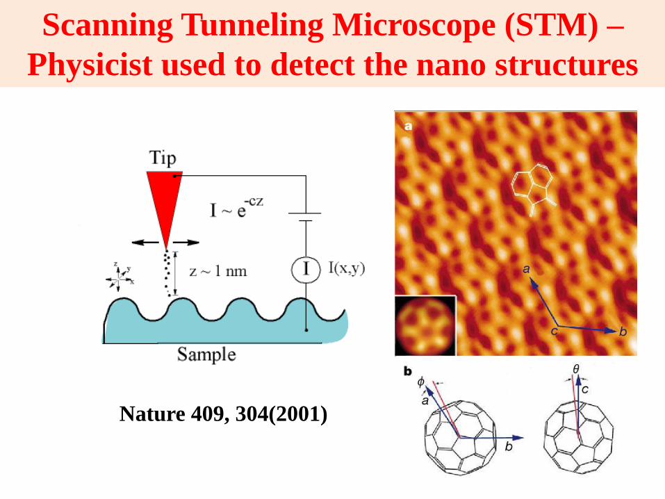
Scanning Tunneling Microscope (STM) –
Physicist used to detect the nano structures
Nature 409, 304(2001)

C60/Cu(111) case: “optimal” doping (e.g., 3 e- per C60) achieved purely through interface reconstruction. Combined techniques of STS, STM, PES, LEED I-V, and ab-initio theory are used in this study.
Naïve case! thought to be true
Reality… structure-doping correlation
Doping-structure correlation at fullerene/metal interface (interface engineering)
W. W. Pai et al., Phys. Rev. Lett. 104, 036103 (2010)
Implication: electronic property of molecule-electrode contact must consider structural details at the interface
72
(IV) Quantum Spin

73
Spin and Nano technology
Electron Spin is the smallest unit of magetism, Came from Quantum Mechanics
N
S

74
Often being used for magnetic recording ~30 billion market
Spintronics Electronics

New generation of computer
75
Compulttion and storage
in one shot
When turn-on,
it is ready!
76
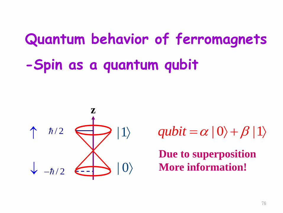
Quantum behavior of ferromagnets
-Spin as a quantum qubit
/ 2
|1
| 0
z
/ 2 | 0 |1qubit
Due to superposition
More information!

Can we take the “charge” out of Spintronics ?
To generate pure spin current ! Courtesy Claude Chappert, Université Paris Su, INTERMAG 2008, Madrid, Spain

Spintronics vs Electronics
Reducing the heat generated in traditional electronics is
a major driving force for developing spintronics.
Spin-based transistors do not strictly rely on the raising or
lowering of electrostatic barriers, hence it may overcome
scaling limits in charge-based transistors.
Spin transport in semiconductors may lead to
dissipationless transfer of information by pure spin currents.
Allow computer speed and power consumption to move
beyond limitations of current technologies.
78

Reliable generation of pure spin currents !
Spin Hall effect (2004)
Spin Pumping (2006)
Inverse Spin Hall effect (2006)
Spin Seebeck effect (2008)
Spin Caloritronics (2010)
79

80
Major Qauntum Effect
at the nano scale
• Interference
• Quantization
• Tunneling
• Quantum Spin

The Fourth Lesson:
Innovations of
nano structures and
nano materials
for various applications

Au NP @ SiOx NW
Color-selective Optical
Switch, SPR-enhanced
Sensor
Ag NP on Si NT
SERS:
Molecule/Bio-sensing
GaN Nanobridge
100 nm
Pt-Ru NP on CNx NT
High-gain Photo-detector,
Solar Cells, Bio-sensor
Fuel Cells,
Supercapacitors
Overview of Advanced Materials Laboratory
Li-Chyong Chen
Center for Condensed Matter Sciences
National Taiwan University

Core-shell
Nanotip
Wire/Rod
Tube
Belt
Peapod Adv. Mater. 14, 1847 (2002)
Nature Mater. 5, 102 (2006)
JACS 123, 2791 (2001) APL 81, 22 (2002)
JACS 127, 2820 (2005)
APL 88, 241905 (2006)
APL 90, 213104 (2007)
Adv. Func. Mater. 18, 938 (2008)
Small 4, 925 (2008)
Analytical Chem. 81, 36 (2009)
APL 79, 3179 (2001)
APL 81, 4189 (2002)
Adv. Func. Mater. 12, 687 (2002)
APL 86, 203119 (2005)
Chem. Mater. 17, 3749 (2005)
JACS 128, 8368 (2006)
PRB 75, 195429 (2007)
JACS 130, 3543 (2008)
APL 81, 1312 (2002)
Nano. Lett. 3, 537 (2003)
Chapter 9, pp. 259-309,
Nanowires and nanobelts, Z.L.
Wang Ed., Kluwer (2004)
Adv. Func. Mater. 16, 537 (2006)
APL 90, 123109 (2007)
Adv. Mater. 19, 4524 (2007)
APL 83, 1420 (2003)
Nano. Lett. 4, 471 (2004)
Chem. Mater. 17, 553 (2005)
Adv. Func. Mater. 15, 783 (2005)
APL 86, 203119 (2005)
US Patent 6,960,528,B2
APL 89, 143105 (2006)
Nature Nanotech. 2, 170 (2007)
Nano Lett. 9, 1839 (2009
Brush
Adv. Func. Mater. 14, 233 (2004)
Other Thin Films:
APL 86, 21911 (2005)
APL 86, 83104 (2005)
APL 86, 161901 (2005)
APL 87, 261915 (2005)
JVST B 24, 87 (2006)
APL 88, 73515 (2006)
Adv. Mater. 21, 759 (2009)
The Nano-world at CCMS-AML:
a Fruitful Research Field with Technology Implications

Si Nanotips-Array and their Hetero-junctions:
On-chip, IC-compatible * Antireflection:
Broadband (uv-terahertz), Omnidirectional (>70o)
* Electroluminescence in ZnO/SiNTs:
IR emission, x10 higher; turn-on ~3V, x2 lower than film
* Magneto-resistance in LSMO/SiNTs:
Room-temp. MR at lower bias and magnetic field
H
ZnO/SiNT IR-LED
Nature-Nanotechnology
2 (2007) 770
Nano Letters
9 (2009) 1839
Promising high-density memory:
On-going
n-Si
p-CMR
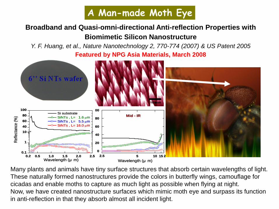
Broadband and Quasi-omni-directional Anti-reflection Properties with
Biomimetic Silicon Nanostructure
Y. F. Huang, et al., Nature Nanotechnology 2, 770-774 (2007) & US Patent 2005
Featured by NPG Asia Materials, March 2008
0
20
40
60
80
1004000 3000 2000 1000
2.5
500
20
Y A
xis
Titl
e
X Axis Title
Si substrate
SiNTs , L= 1.6 m
SiNTs , L= 5.5 m
SiNTs , L= 16 m
5 10 15
Mid - IR
Wavenumber (cm-1)
Wavelength (μ m)
Re
flect
ance
(%
)
0
20
40
60
80
1004000 3000 2000 1000
2.5
500
20
Y A
xis
Titl
e
X Axis Title
Si substrate
SiNTs , L= 1.6 m
SiNTs , L= 5.5 m
SiNTs , L= 16 m
5 10 15
Mid - IR
Wavenumber (cm-1)
Wavelength (μ m)
Re
flect
ance
(%
)
0.5 1.0 1.5 2.0 2.5
0.1
1
10
40
60
80
100
0.2
UV-VIS-NIR
Si substrate
SiNTs , L= 1.6 m
SiNTs , L= 5.5 m
SiNTs , L= 16.0 m
Ref
lect
ance
(%
)
Wavelength ( m)
Si-Wafer-N+
ECR 833-SiNTs -N+-R%
ECR 852 SiNTs-N+
ECR 835-SiNTs-N+
Re
flect
ance
(%
)
Wavelength (μ m)0.5 1.0 1.5 2.0 2.5
0.1
1
10
40
60
80
100
0.2
UV-VIS-NIR
Si substrate
SiNTs , L= 1.6 m
SiNTs , L= 5.5 m
SiNTs , L= 16.0 m
Ref
lect
ance
(%
)
Wavelength ( m)
Si-Wafer-N+
ECR 833-SiNTs -N+-R%
ECR 852 SiNTs-N+
ECR 835-SiNTs-N+
Re
flect
ance
(%
)
Wavelength (μ m)
Many plants and animals have tiny surface structures that absorb certain wavelengths of light.
These naturally formed nanostructures provide the colors in butterfly wings, camouflage for
cicadas and enable moths to capture as much light as possible when flying at night.
Now, we have created nanostructure surfaces which mimic moth eye and surpass its function
in anti-reflection in that they absorb almost all incident light.
A Man-made Moth Eye

On-chip Fabrication of Well Aligned and Contact Barrier-Free GaN
Nanobridge Devices with Ultrahigh Photocurrent Responsivity
R. S. Chen, et al., Small 4, 925-929 (2008)
5μm
GaN nano-bridge
wafer process
doped GaN
c-plane Sapphire
Ni GaN NW
W probe
h
e- h+
Building a Nano-scale Bridge On-chip
• Nanowire: Naturally formed core-shell structure, 1D electron gas-like property
• On-chip process for building GaN nanobridge devices, which provide a large
surface area, short transport path, and high responsivity for next-generation
sensors and detectors
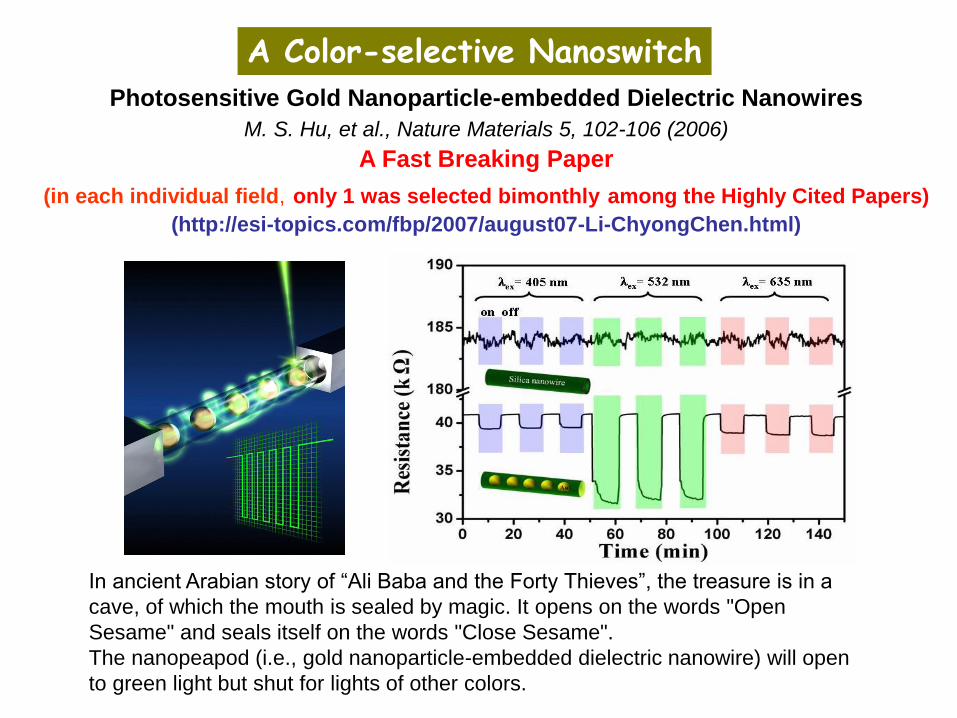
Photosensitive Gold Nanoparticle-embedded Dielectric Nanowires
M. S. Hu, et al., Nature Materials 5, 102-106 (2006)
A Fast Breaking Paper
(in each individual field, only 1 was selected bimonthly among the Highly Cited Papers)
(http://esi-topics.com/fbp/2007/august07-Li-ChyongChen.html)
In ancient Arabian story of “Ali Baba and the Forty Thieves”, the treasure is in a
cave, of which the mouth is sealed by magic. It opens on the words "Open
Sesame" and seals itself on the words "Close Sesame".
The nanopeapod (i.e., gold nanoparticle-embedded dielectric nanowire) will open
to green light but shut for lights of other colors.
A Color-selective Nanoswitch

Ultrafine Pt Nanoparticles Uniformly Dispersed on Arrayed Carbon Nanotubes
with High Electrochemical Activity at Low Loading of Precious Metal
C. L. Sun, et al., Chemistry of Materials 17, 3749-3753 (2005)
C. H. Wang, et al., J. Power Sources 171, 55-62 (2007)
1.4 1.6 1.8 2.0 2.2 2.4 2.6 2.8 3.0 3.2 3.40
5
10
15
20
Num
ber
Diameter(nm)
2 nm
• Direct methanol fuel cell is promising power generator with a wide range of
applications from portable electronic devices to automobiles.
• Nanotubes-Pt/Ru composites are highly efficient in loading precious metals.
Only one tenth of metal loading, in comparison to the conventional, is needed.
Next-generation Energy Solution (I): Fuel Cell with Low-loading of Precious Metals
0 100 200 300 400 500 6000
20
40
60
80
100 0.4 mg/cm2 Pt-Ru/CNT-carbon cloth
3.0 mg/cm2 60% Pt-Ru/C (ETEK)
4.0 mg/cm2 30% Pt-Ru/C (Home made)
4.0 mg/cm2 20% Pt-Ru/CNT (Home made)
P /
mW
/cm
2
j / mA/cm2

RuO2on N-doped
CNT composites (BEI)
(SEI)
• 4 fold increase in capacitance
• Optimal capacitance of 1380 F/g at 600 mV/s
(theory: 1450 F/g)
• Output current as high as 23 mA/cm2
• Stable at high scan rate
• 10 fold increase in charge-discharge rate
Next-generation Energy Solution (II): High-performance Supercapacitor
Ultrafast Charging-discharging Capacitive Property of RuO2 Nanoparticles on
Carbon Nanotubes Using Nitrogen Incorporation
W. C. Fang, et al., Electrochemistry Communications 9, 239-244 (2007)
W. C. Fang, et al., J. Electrochemical Society 155, K15-K18 (2008)
0.0 0.2 0.4 0.6 0.8 1.0-70
0
70
Scan rate = 600 mV/s
Cap
acit
an
ce (
mF
/cm
2)
E (V vs. Ag/AgCl)
CNx NTs
RuO2 films
CNx NTs-RuO
2
0 5 10 15 20
0.00
0.75
1.50I = 23 mA/cm
2
Scan rate = 600 mV/s
Po
ten
tial (V
vs. A
g/A
gC
l)
Time (s)
Nanocomposites
RuO2 films

The Fifth Lesson:
Nano photonics
and
Bio-applications

Dr. Juen-Kai Wang, CCMS, NTU
Nano-photonics and Plasmonics
Near-field examination of blue-ray discs
Scattering-type SNOM reveals sub-10 nm optical signature.
The optical contrasts of the dark and the bright regions in near-field image of phase-
change layer correspond to amorphous and polycrystalline AgInSbTe, respectively.
Small bright spots with a size of ~30 nm emerge within the dark region, corresponding to
the nano-sized ordered domains in the TEM image.
s-SNOM provides a direct optical probe in nanometer scale for high density optical
storage media.
J. Y. Chu et al., Appl. Phys. Lett. 95, 103105 (2009).
S-SNOM setup

Dr. Juen-Kai Wang, CCMS, NTU
Creating Monodispersed Ordered Arrays of Surface-Magic-Clusters
and Anodic Alumia Nanochannels by Constrained Self-organization
Prof. Yuh-Lin Wang 王玉麟 IAMS Academia Sinica, Taiwan

Dr. Juen-Kai Wang, CCMS, NTU
93
A High Sensitivity and High Speed Biomedical Diagnostic
Technology using SERS
Prof. Yuh-Lin Wang 王玉麟 IAMS Academia Sinica, Taiwan

Dr. Juen-Kai Wang, CCMS, NTU
SERS detection of bacterial cell wall
Sensitive and stable SERS profiles based on our substrates readily reflect different
bacterial cell walls found in Gram-positive, Gram-negative, and mycobacteria group.
Characteristic changes in SERS profile are recognized in the drug-sensitive bacteria of
antibiotic exposure, which could be used to differentiate them from the drug-resistant ones.
H.-H. Wang et al., Adv. Mater. 18, 491 (2006); T.-T. Liu et al., PLoS ONE 4, e5470 (2009).

The End