programmable single-phase energy metering ic with tamper ... fileenergy in a power line system using...
TRANSCRIPT
This is information on a product in full production.
January 2013 Doc ID 17728 Rev 4 1/53
53
STPM10
Programmable single-phase energy metering ICwith tamper detection
Datasheet − production data
Features■ Measures active, reactive, and apparent
energies
■ Current, voltage RMS and instantaneous measurement
■ Frequency measurement
■ Ripple-free active energy pulsed output
■ Live and neutral monitoring for tamper detection
■ Fast and simple one-point digital calibration over the whole current range
■ Integrated linear voltage regulators for digital and analog supply
■ Selectable RC or crystal oscillator
■ Supports 50 - 60 Hz - IEC62052-11, IEC62053-2x specifications
■ Less than 0.1% error in the 1000:1 range
■ Precision voltage reference: 1.23 V with 30 ppm/°C max
DescriptionThe STPM10 is designed for effective measurement of active, reactive and apparent energy in a power line system using current transformer and shunt sensors. The device can be implemented for peripheral measurement in a microcontroller-based single-phase or poly-phase energy meter. The STPM10 consists of two main sections: analog and digital. The analog part is composed of preamplifier and first-order sigma-delta A/D converter blocks, a band-gap voltage
reference and low-drop voltage regulator. The digital part is composed of system control,
oscillator, hard-wired DSP and SPI interface. There is also an internal volatile memory, which is controlled through the SPI by means of a dedicated command set. The configured bits are used for configuration and calibration purposes. From a pair of sigma-delta output signals produced by the analog section, the DSP unit computes the amount of active, reactive and apparent energy consumed, as well as the RMS and instantaneous voltage and current values. The results of the computation are available as pulse frequencies and states on the digital outputs of the device, or as data bits in a data stream, which can be read from the device by means of the SPI interface. The system bus interface is also used for temporary programming of bits of internal volatile memory. The STPM10 generates an output signal with a pulse frequency proportional to the energy, and this signal is used in the calibration phase of the energy metering application.
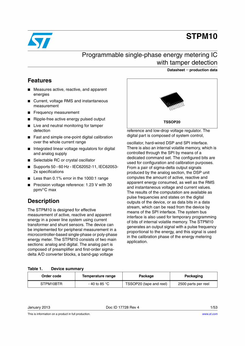
TSSOP20
Table 1. Device summary
Order code Temperature range Package Packaging
STPM10BTR - 40 to 85 °C TSSOP20 (tape and reel) 2500 parts per reel
www.st.com
Contents STPM10
2/53 Doc ID 17728 Rev 4
Contents
1 Schematic diagram . . . . . . . . . . . . . . . . . . . . . . . . . . . . . . . . . . . . . . . . . . 6
2 Pin configuration . . . . . . . . . . . . . . . . . . . . . . . . . . . . . . . . . . . . . . . . . . . 7
3 Maximum ratings . . . . . . . . . . . . . . . . . . . . . . . . . . . . . . . . . . . . . . . . . . . . 8
4 Electrical characteristics . . . . . . . . . . . . . . . . . . . . . . . . . . . . . . . . . . . . . 9
5 Terminology . . . . . . . . . . . . . . . . . . . . . . . . . . . . . . . . . . . . . . . . . . . . . . . 12
5.1 Measurement error . . . . . . . . . . . . . . . . . . . . . . . . . . . . . . . . . . . . . . . . . . 12
5.2 ADC offset error . . . . . . . . . . . . . . . . . . . . . . . . . . . . . . . . . . . . . . . . . . . . 12
5.3 Gain error . . . . . . . . . . . . . . . . . . . . . . . . . . . . . . . . . . . . . . . . . . . . . . . . . 12
5.4 Power supply DC and AC rejection . . . . . . . . . . . . . . . . . . . . . . . . . . . . . 12
5.5 Conventions . . . . . . . . . . . . . . . . . . . . . . . . . . . . . . . . . . . . . . . . . . . . . . . 12
6 Typical performance characteristics . . . . . . . . . . . . . . . . . . . . . . . . . . . 13
7 Theory of operation . . . . . . . . . . . . . . . . . . . . . . . . . . . . . . . . . . . . . . . . 16
7.1 General operation description . . . . . . . . . . . . . . . . . . . . . . . . . . . . . . . . . 16
7.2 Analog inputs . . . . . . . . . . . . . . . . . . . . . . . . . . . . . . . . . . . . . . . . . . . . . . 16
7.3 ΣΔ A/D converters . . . . . . . . . . . . . . . . . . . . . . . . . . . . . . . . . . . . . . . . . . 18
7.4 Zero-crossing detection . . . . . . . . . . . . . . . . . . . . . . . . . . . . . . . . . . . . . . 19
7.5 Period and line voltage measurement . . . . . . . . . . . . . . . . . . . . . . . . . . . 19
7.6 Power supply . . . . . . . . . . . . . . . . . . . . . . . . . . . . . . . . . . . . . . . . . . . . . . 21
7.7 Load monitoring . . . . . . . . . . . . . . . . . . . . . . . . . . . . . . . . . . . . . . . . . . . . 21
7.8 Error detection . . . . . . . . . . . . . . . . . . . . . . . . . . . . . . . . . . . . . . . . . . . . . 22
7.9 Tamper detection module . . . . . . . . . . . . . . . . . . . . . . . . . . . . . . . . . . . . . 22
7.9.1 Detailed operational description . . . . . . . . . . . . . . . . . . . . . . . . . . . . . . 23
7.10 Phase compensation . . . . . . . . . . . . . . . . . . . . . . . . . . . . . . . . . . . . . . . . 24
7.11 Clock generator . . . . . . . . . . . . . . . . . . . . . . . . . . . . . . . . . . . . . . . . . . . . 25
7.11.1 RC startup procedure . . . . . . . . . . . . . . . . . . . . . . . . . . . . . . . . . . . . . . 25
7.12 Resetting the STPM10 . . . . . . . . . . . . . . . . . . . . . . . . . . . . . . . . . . . . . . . 26
7.13 Using the STPM10 in microcontroller-based meters . . . . . . . . . . . . . . . . 26

STPM10 Contents
Doc ID 17728 Rev 4 3/53
7.14 Energy to frequency conversion . . . . . . . . . . . . . . . . . . . . . . . . . . . . . . . . 27
7.15 Status bits . . . . . . . . . . . . . . . . . . . . . . . . . . . . . . . . . . . . . . . . . . . . . . . . 28
7.16 Programming the STPM10 . . . . . . . . . . . . . . . . . . . . . . . . . . . . . . . . . . . . 29
7.16.1 Data records . . . . . . . . . . . . . . . . . . . . . . . . . . . . . . . . . . . . . . . . . . . . . 29
7.17 Configuration bits . . . . . . . . . . . . . . . . . . . . . . . . . . . . . . . . . . . . . . . . . . . 29
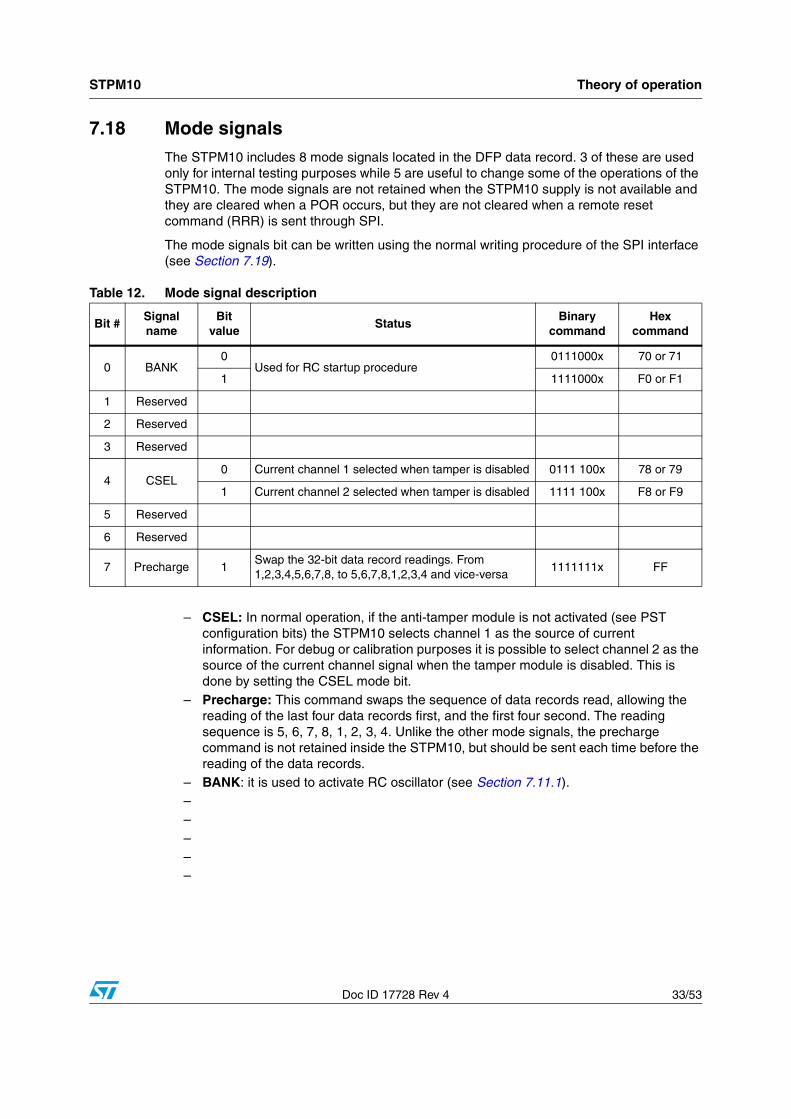
7.18 Mode signals . . . . . . . . . . . . . . . . . . . . . . . . . . . . . . . . . . . . . . . . . . . . . . 33
7.19 SPI interface . . . . . . . . . . . . . . . . . . . . . . . . . . . . . . . . . . . . . . . . . . . . . . . 34
7.20 Remote reset . . . . . . . . . . . . . . . . . . . . . . . . . . . . . . . . . . . . . . . . . . . . . . 35
7.21 Reading data records . . . . . . . . . . . . . . . . . . . . . . . . . . . . . . . . . . . . . . . . 35
7.22 Writing procedure . . . . . . . . . . . . . . . . . . . . . . . . . . . . . . . . . . . . . . . . . . . 37
7.22.1 Interfacing the standard 3-wire SPI with the STPM10 SPI . . . . . . . . . . 38
7.23 Energy calculation algorithm . . . . . . . . . . . . . . . . . . . . . . . . . . . . . . . . . . 39
7.23.1 Active power . . . . . . . . . . . . . . . . . . . . . . . . . . . . . . . . . . . . . . . . . . . . . 39
7.23.2 Reactive power . . . . . . . . . . . . . . . . . . . . . . . . . . . . . . . . . . . . . . . . . . . 41
7.23.3 Apparent power and RMS values . . . . . . . . . . . . . . . . . . . . . . . . . . . . . 42
7.24 STPM10 calibration . . . . . . . . . . . . . . . . . . . . . . . . . . . . . . . . . . . . . . . . . 43
8 Application design . . . . . . . . . . . . . . . . . . . . . . . . . . . . . . . . . . . . . . . . . 46
9 Package mechanical data . . . . . . . . . . . . . . . . . . . . . . . . . . . . . . . . . . . . 48
10 Revision history . . . . . . . . . . . . . . . . . . . . . . . . . . . . . . . . . . . . . . . . . . . 52

List of tables STPM10
4/53 Doc ID 17728 Rev 4
List of tables
Table 1. Device summary . . . . . . . . . . . . . . . . . . . . . . . . . . . . . . . . . . . . . . . . . . . . . . . . . . . . . . . . . . 1Table 2. Pin description . . . . . . . . . . . . . . . . . . . . . . . . . . . . . . . . . . . . . . . . . . . . . . . . . . . . . . . . . . . 7Table 3. Absolute maximum ratings . . . . . . . . . . . . . . . . . . . . . . . . . . . . . . . . . . . . . . . . . . . . . . . . . . 8Table 4. Thermal data. . . . . . . . . . . . . . . . . . . . . . . . . . . . . . . . . . . . . . . . . . . . . . . . . . . . . . . . . . . . . 8Table 5. Electrical characteristics . . . . . . . . . . . . . . . . . . . . . . . . . . . . . . . . . . . . . . . . . . . . . . . . . . . . 9Table 6. Gain of voltage and current channels . . . . . . . . . . . . . . . . . . . . . . . . . . . . . . . . . . . . . . . . . 17Table 7. Configuration of current sensors. . . . . . . . . . . . . . . . . . . . . . . . . . . . . . . . . . . . . . . . . . . . . 17Table 8. No-load detection thresholds . . . . . . . . . . . . . . . . . . . . . . . . . . . . . . . . . . . . . . . . . . . . . . . 22Table 9. LED pin configuration . . . . . . . . . . . . . . . . . . . . . . . . . . . . . . . . . . . . . . . . . . . . . . . . . . . . . 27Table 10. Status bit description . . . . . . . . . . . . . . . . . . . . . . . . . . . . . . . . . . . . . . . . . . . . . . . . . . . . . 28Table 11. Configuration bit map . . . . . . . . . . . . . . . . . . . . . . . . . . . . . . . . . . . . . . . . . . . . . . . . . . . . . 30Table 12. Mode signal description . . . . . . . . . . . . . . . . . . . . . . . . . . . . . . . . . . . . . . . . . . . . . . . . . . . 33Table 13. Working point settings . . . . . . . . . . . . . . . . . . . . . . . . . . . . . . . . . . . . . . . . . . . . . . . . . . . . 44Table 14. Device constants . . . . . . . . . . . . . . . . . . . . . . . . . . . . . . . . . . . . . . . . . . . . . . . . . . . . . . . . 44Table 15. Resistor divider ratio . . . . . . . . . . . . . . . . . . . . . . . . . . . . . . . . . . . . . . . . . . . . . . . . . . . . . . 46Table 16. Current channel typical components . . . . . . . . . . . . . . . . . . . . . . . . . . . . . . . . . . . . . . . . . 46Table 17. Footprint data . . . . . . . . . . . . . . . . . . . . . . . . . . . . . . . . . . . . . . . . . . . . . . . . . . . . . . . . . . . 51Table 18. Document revision history . . . . . . . . . . . . . . . . . . . . . . . . . . . . . . . . . . . . . . . . . . . . . . . . . 52

STPM10 List of figures
Doc ID 17728 Rev 4 5/53
List of figures
Figure 1. Block diagram . . . . . . . . . . . . . . . . . . . . . . . . . . . . . . . . . . . . . . . . . . . . . . . . . . . . . . . . . . . . 6Figure 2. Pin connections (top view) . . . . . . . . . . . . . . . . . . . . . . . . . . . . . . . . . . . . . . . . . . . . . . . . . . 7Figure 3. Supply current vs. supply voltage, TA = 25 °C (f = 4.194MHz, 8.192MHz) . . . . . . . . . . . . 13Figure 4. RC oscillator frequency vs. VCC,
R = 12 kW, TA = 25 °C . . . . . . . . . . . . . . . . . . . . . . . . . . . . . . . . . . . . . . . . . . . . . . . . . . . . 13Figure 5. RC oscillator: frequency jitter vs. temperature . . . . . . . . . . . . . . . . . . . . . . . . . . . . . . . . . . 13Figure 6. Analog voltage regulator: line - load regulation . . . . . . . . . . . . . . . . . . . . . . . . . . . . . . . . . 13Figure 7. Digital voltage regulator: line - load regulation . . . . . . . . . . . . . . . . . . . . . . . . . . . . . . . . . . 14Figure 8. Voltage channel linearity at different VCC voltages . . . . . . . . . . . . . . . . . . . . . . . . . . . . . . 14Figure 9. Power supply AC rejection vs. VCC . . . . . . . . . . . . . . . . . . . . . . . . . . . . . . . . . . . . . . . . . . 14Figure 10. Power supply DC rejection vs. VCC . . . . . . . . . . . . . . . . . . . . . . . . . . . . . . . . . . . . . . . . . . 14Figure 11. Error over dynamic range gain dependence. . . . . . . . . . . . . . . . . . . . . . . . . . . . . . . . . . . . 14Figure 12. Primary current channel linearity at different VCC . . . . . . . . . . . . . . . . . . . . . . . . . . . . . . . 14Figure 13. Gain response of ΣΔ A/D converters . . . . . . . . . . . . . . . . . . . . . . . . . . . . . . . . . . . . . . . . . 15Figure 14. First-order ΣΔ A/D converter . . . . . . . . . . . . . . . . . . . . . . . . . . . . . . . . . . . . . . . . . . . . . . . . 18Figure 15. ZCR signal . . . . . . . . . . . . . . . . . . . . . . . . . . . . . . . . . . . . . . . . . . . . . . . . . . . . . . . . . . . . . 19Figure 16. LIN and BFR signals . . . . . . . . . . . . . . . . . . . . . . . . . . . . . . . . . . . . . . . . . . . . . . . . . . . . . . 20Figure 17. Band-gap temperature variation . . . . . . . . . . . . . . . . . . . . . . . . . . . . . . . . . . . . . . . . . . . . . 21Figure 18. Timings of tamper module - primary channel selected . . . . . . . . . . . . . . . . . . . . . . . . . . . . 23Figure 19. Timings of tamper module - secondary channel selected. . . . . . . . . . . . . . . . . . . . . . . . . . 24Figure 20. Different oscillator circuits with (a) quartz, (b) internal oscillator, (c) external source . . . . . 25Figure 21. STPM10 data record map. . . . . . . . . . . . . . . . . . . . . . . . . . . . . . . . . . . . . . . . . . . . . . . . . . 29Figure 22. Timing for providing remote reset request . . . . . . . . . . . . . . . . . . . . . . . . . . . . . . . . . . . . . 35Figure 23. Data record reconstruction . . . . . . . . . . . . . . . . . . . . . . . . . . . . . . . . . . . . . . . . . . . . . . . . . 36Figure 24. Timing for data record reading . . . . . . . . . . . . . . . . . . . . . . . . . . . . . . . . . . . . . . . . . . . . . . 36Figure 25. Timing for writing configuration and mode bits . . . . . . . . . . . . . . . . . . . . . . . . . . . . . . . . . . 37Figure 26. Active energy computation diagram . . . . . . . . . . . . . . . . . . . . . . . . . . . . . . . . . . . . . . . . . . 40Figure 27. STPM10 reference schematic with one current transformer and one shunt. . . . . . . . . . . . 47Figure 28. TSSOP20 footprint recommended data . . . . . . . . . . . . . . . . . . . . . . . . . . . . . . . . . . . . . . . 51
Schematic diagram STPM10
6/53 Doc ID 17728 Rev 4
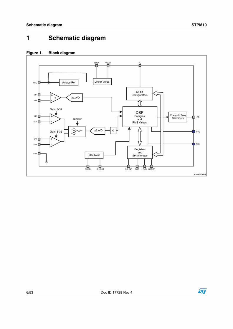
1 Schematic diagram
Figure 1. Block diagram
VDDA VDDD VO
LED
WDG
ZCR
SDA/TDSYNSCSSCL/NCCLKOUTCLKIN
VSS
IIN2
IIP2
IIN1
IIPI
VIN
VIP
VCC Voltage Ref Linear Vregs
56-bitConfigurators
DSPEnergies
andRMS Values
Energy to FreqConverters
Registersand
SPI InterfaceOscillator
ΔΣ A/D
+
-
Gain: 8-32
Tamper+
-
+
-
ΔΣ A/D
Gain: 8-32
4
φ
AM00176v1
STPM10 Pin configuration
Doc ID 17728 Rev 4 7/53
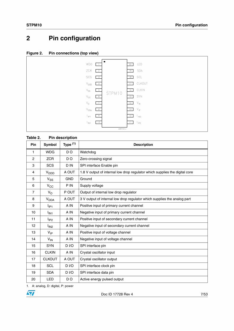
2 Pin configuration
Figure 2. Pin connections (top view)
Table 2. Pin description
Pin Symbol Type (1) Description
1 WDG D O Watchdog
2 ZCR D O Zero-crossing signal
3 SCS D IN SPI interface Enable pin
4 VDDD A OUT 1.8 V output of internal low drop regulator which supplies the digital core
5 VSS GND Ground
6 VCC P IN Supply voltage
7 VO P OUT Output of internal low drop regulator
8 VDDA A OUT 3 V output of internal low drop regulator which supplies the analog part
9 IIP1 A IN Positive input of primary current channel
10 IIN1 A IN Negative input of primary current channel
11 IIP2 A IN Positive input of secondary current channel
12 IIN2 A IN Negative input of secondary current channel
13 VIP A IN Positive input of voltage channel
14 VIN A IN Negative input of voltage channel
15 SYN D I/O SPI interface pin
16 CLKIN A IN Crystal oscillator input
17 CLKOUT A OUT Crystal oscillator output
18 SCL D I/O SPI interface clock pin
19 SDA D I/O SPI interface data pin
20 LED D O Active energy pulsed output
1. A: analog, D: digital, P: power

Maximum ratings STPM10
8/53 Doc ID 17728 Rev 4
3 Maximum ratings
Note: Absolute maximum ratings are those values beyond which damage to the device may occur. Functional operation under these condition is not implied.
Table 3. Absolute maximum ratings
Symbol Parameter Value Unit
VCC DC input voltage -0.3 to 6 V
IPIN Current on any pin (sink/source) ± 150 mA
VIDInput voltage at digital pins (SCS, ZCR, WDG, SYN, SDA, SCL, LED)
-0.3 to VCC + 0.3 V
VIA Input voltage at analog pins (IIP1, IIN1, IIP2, IIN2, VIP, VIN) -0.7 to 0.7 V
ESD Human body model (all pins) ± 3.5 kV
TOP Operating ambient temperature - 40 to 85 °C
TJ Junction temperature - 40 to 150 °C
TSTG Storage temperature range - 55 to 150 °C
Table 4. Thermal data
Symbol Parameter Value Unit
RthJA Thermal resistance junction-to-ambient 114.5 (1) °C/W
1. This value is based on a single-layer PCB, JEDEC standard test board.

STPM10 Electrical characteristics
Doc ID 17728 Rev 4 9/53
4 Electrical characteristics
VCC = 5 V, TA = 25 °C,100 nF to 1 µF between VDDA and VSS, 100 nF to 1 µF between VDDD and VSS, 100 nF to 1 µF between VCC and VSS unless otherwise specified.
Table 5. Electrical characteristics
Symbol Parameter Test conditions Min. Typ. Max. Unit
Energy measurement accuracy
fBW Effective bandwidth Limited by digital filtering (-3 dB) 4 800 Hz
eAW Accuracy of active power Over 1 to 1000 of dynamic range 0.1 %
eRW Accuracy of reactive powerOver 1 to 1000 of dynamic range
0.1 %
eSW Accuracy of apparent power Over 1 to 500 of dynamic range 0.1 %
SNR Signal-to-noise ratio Over the entire bandwidth 52 db
PSRRDC Power supply DC rejection
Voltage signal: 200 mVrms/50HzCurrent signal: 10 mVrms/50HzfCLK= 4.194 MHzVCC=3.3V±10%, 5V±10%
0.2 %
PSRRAC Power supply AC rejection
Voltage signal: 200 mVrms/50 HzCurrent signal: 10 mVrms/50 HzfCLK= 4.194 MHzVCC=3.3 V+0.2 Vrms1@100 HzVCC=5.0 V+0.2 Vrms1@100 Hz
0.1 %
General section
VCC Operating supply voltage 3.165 5.5 V
ICCSupply current. Configuration registers cleared
4 MHz; VCC=5 V 3 4 mA
8 MHz; VCC=5 V 5 6 mA
POR Power on reset on VCC 2.5 V
VDDA Analog supply voltage 2.85 3.00 3.15 V
VDDD Digital supply Voltage 1.725 1.80 1.875 V
fCLK Oscillator clock frequencyMDIV bit=0 4.000 4.194 MHz
MDIV bit=1 8.000 8.192 MHz
fLINE Nominal line frequency 45 65 Hz
ILATCHCurrent injection latch-up immunity
300 mA
Analog inputs (IIP1, IIN1, IIP2, IIN2, VIP, VIN)
VMAX Maximum input signal levels
Voltage channel -0.3 +0.3 V
Current channels:Gain 8X -0.15 +0.15 V
Gain 32X -0.035 +0.035
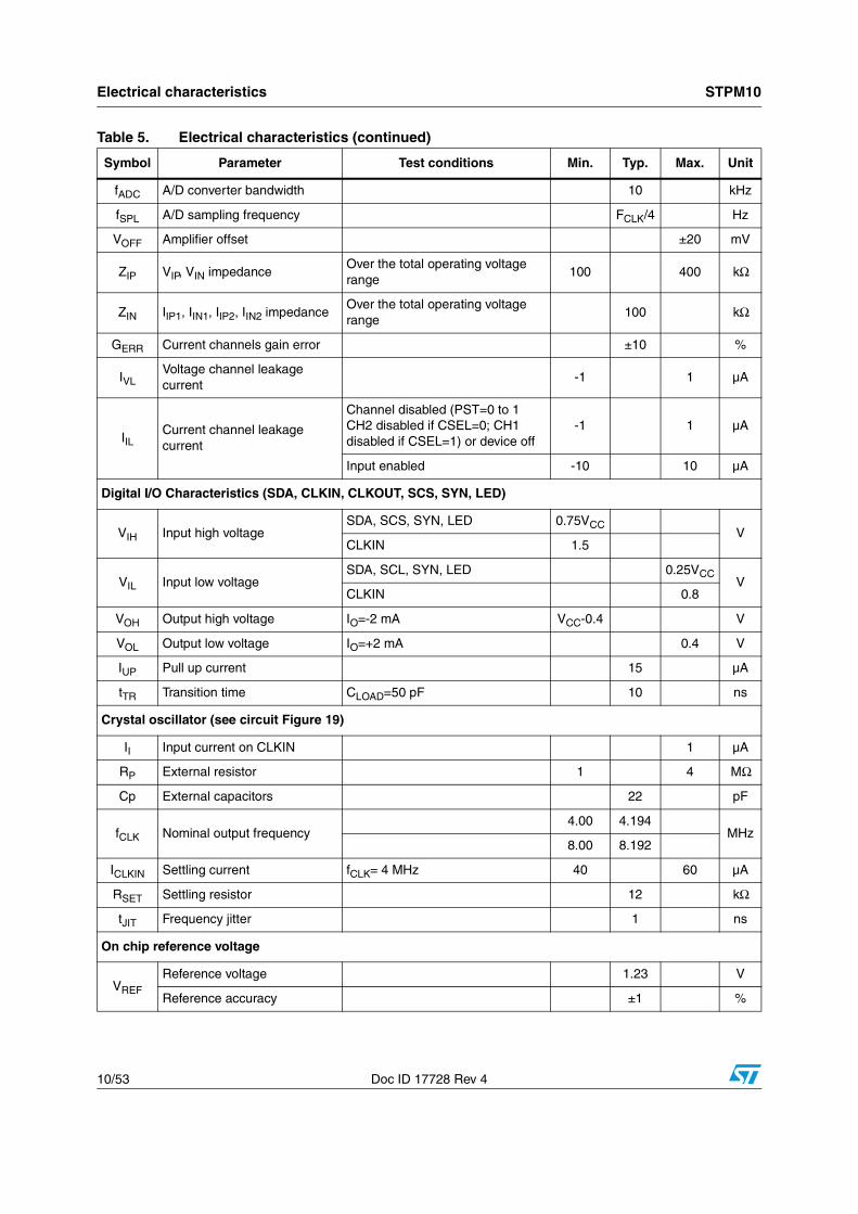
Electrical characteristics STPM10
10/53 Doc ID 17728 Rev 4
fADC A/D converter bandwidth 10 kHz
fSPL A/D sampling frequency FCLK/4 Hz
VOFF Amplifier offset ±20 mV
ZIP VIP, VIN impedanceOver the total operating voltage range
100 400 kΩ
ZIN IIP1, IIN1, IIP2, IIN2 impedanceOver the total operating voltage range
100 kΩ
GERR Current channels gain error ±10 %
IVLVoltage channel leakage current
-1 1 µA
IILCurrent channel leakage current
Channel disabled (PST=0 to 1 CH2 disabled if CSEL=0; CH1 disabled if CSEL=1) or device off
-1 1 µA
Input enabled -10 10 µA
Digital I/O Characteristics (SDA, CLKIN, CLKOUT, SCS, SYN, LED)
VIH Input high voltageSDA, SCS, SYN, LED 0.75VCC
VCLKIN 1.5
VIL Input low voltageSDA, SCL, SYN, LED 0.25VCC
VCLKIN 0.8
VOH Output high voltage IO=-2 mA VCC-0.4 V
VOL Output low voltage IO=+2 mA 0.4 V
IUP Pull up current 15 µA
tTR Transition time CLOAD=50 pF 10 ns
Crystal oscillator (see circuit Figure 19)
II Input current on CLKIN 1 µA
RP External resistor 1 4 MΩ
Cp External capacitors 22 pF
fCLK Nominal output frequency4.00 4.194
MHz8.00 8.192
ICLKIN Settling current fCLK= 4 MHz 40 60 µA
RSET Settling resistor 12 kΩ
tJIT Frequency jitter 1 ns
On chip reference voltage
VREF
Reference voltage 1.23 V
Reference accuracy ±1 %
Table 5. Electrical characteristics (continued)
Symbol Parameter Test conditions Min. Typ. Max. Unit

STPM10 Electrical characteristics
Doc ID 17728 Rev 4 11/53
TC Temperature coefficient After calibration 30 50ppm/°C
SPI interface timing
FSCLKr Data read speed After calibration 32 MHz
FSCLKw Data write speed 100 kHz
tDS Data setup time 20 ns
tDH Data hold time 0 ns
tON Data driver on time 20 ns
tOFF Data driver off time 20 ns
tSYN SYN active width 2/fCLK s
Table 5. Electrical characteristics (continued)
Symbol Parameter Test conditions Min. Typ. Max. Unit
Terminology STPM10
12/53 Doc ID 17728 Rev 4
5 Terminology
5.1 Measurement errorThe error associated with the energy measurement made by the STPM10 is defined as: Percentage error = [STPM10 (reading) - true energy] / true energy
5.2 ADC offset errorThis is the error due to the DC component associated with the analog inputs of the A/D converters. Due to the internal automatic DC offset cancellation, the STPM10 measurement is not affected by DC components in the voltage and current channel. The DC offset cancellation is implemented in the DSP.
5.3 Gain errorThe gain error is gain due to the signal channel gain amplifiers. This is the difference between the measured ADC code and the ideal output code. The difference is expressed as percentage of the ideal code.
5.4 Power supply DC and AC rejectionThis parameter quantifies the STPM10 measurement error as a percentage of the reading when the power supplies are varied. For the PSRRAC measurement, a reading at two nominal supply voltages (3.3 and 5 V) is taken. A second reading is obtained with the same input signal levels when an AC (200 mVRMS/100 Hz) signal is introduced on the supplies. Any error introduced by this AC signal is expressed as a percentage of the reading. For the PSRRDC measurement, a reading at two nominal supply voltages (3.3 and 5 V) is taken. A second reading is obtained with the same input signal levels when the supplies are varied ± 10%. Any error introduced is again expressed as a percentage of the reading.
5.5 ConventionsThe lowest analog and digital power supply voltage is called VSS, which represents system ground (GND). All voltage specifications for digital input/output pins are referred to GND.
Positive currents flow into a pin. Sinking current refers to the current flowing into the pin, and thus it is positive. Sourcing current means that the current is flowing out of the pin, so it is negative.
Timing specifications of signals treated by the digital control part are relative to CLKOUT. This signal is provided by the 4.194 MHz nominal-frequency crystal oscillator or from the internal RC oscillator. An external source of 4.194 MHz or 8.192 MHz can also be used.
Timing specifications of signals from the SPI interface are relative to the SCL, and there is no direct relationship between the clock (SCL) of the SPI interface and the clock of the DSP block. A positive logic convention is used in all equations.
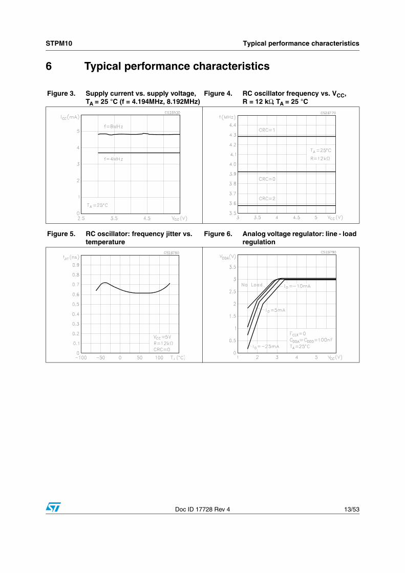
STPM10 Typical performance characteristics
Doc ID 17728 Rev 4 13/53
6 Typical performance characteristics
Figure 3. Supply current vs. supply voltage, TA = 25 °C (f = 4.194MHz, 8.192MHz)
Figure 4. RC oscillator frequency vs. VCC,R = 12 kΩ, TA = 25 °C
Figure 5. RC oscillator: frequency jitter vs. temperature
Figure 6. Analog voltage regulator: line - load regulation
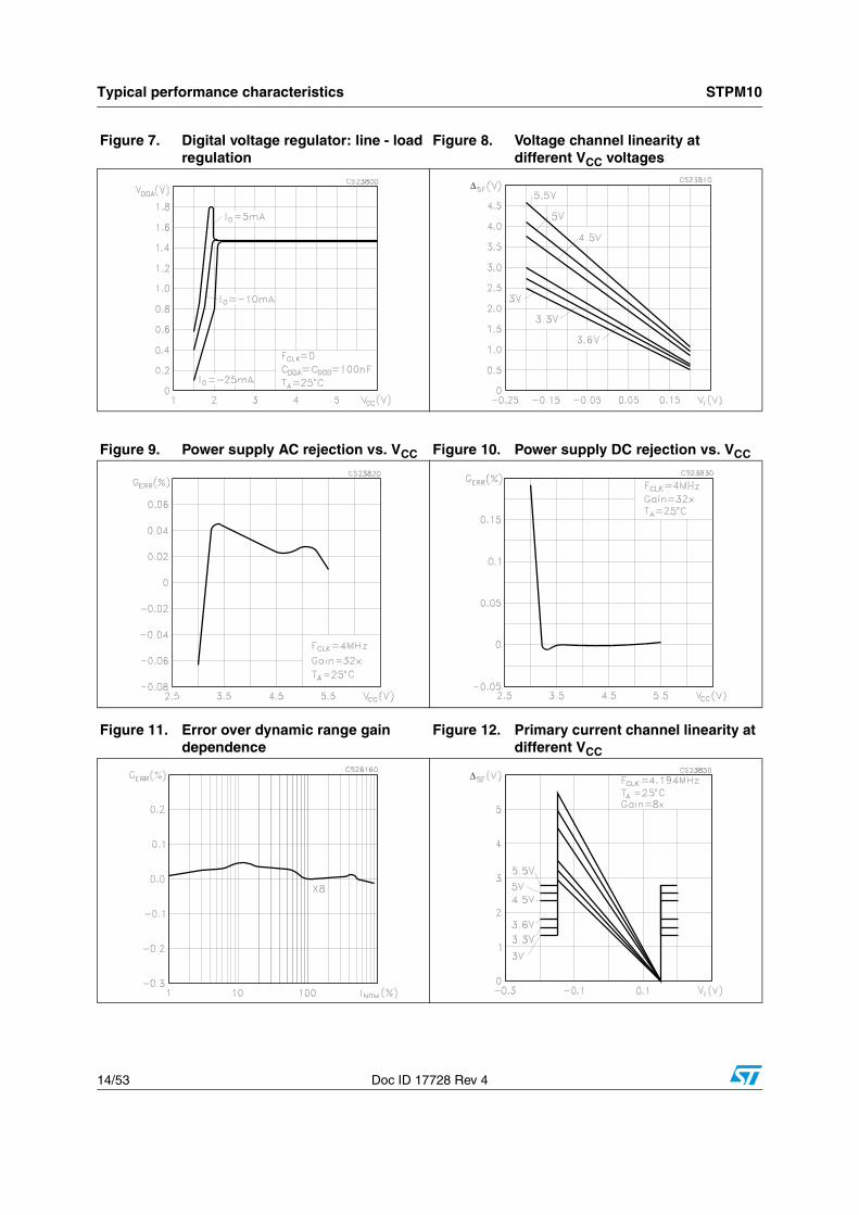
Typical performance characteristics STPM10
14/53 Doc ID 17728 Rev 4
Figure 7. Digital voltage regulator: line - load regulation
Figure 8. Voltage channel linearity at different VCC voltages
Figure 9. Power supply AC rejection vs. VCC Figure 10. Power supply DC rejection vs. VCC
Figure 11. Error over dynamic range gain dependence
Figure 12. Primary current channel linearity at different VCC
STPM10 Typical performance characteristics
Doc ID 17728 Rev 4 15/53
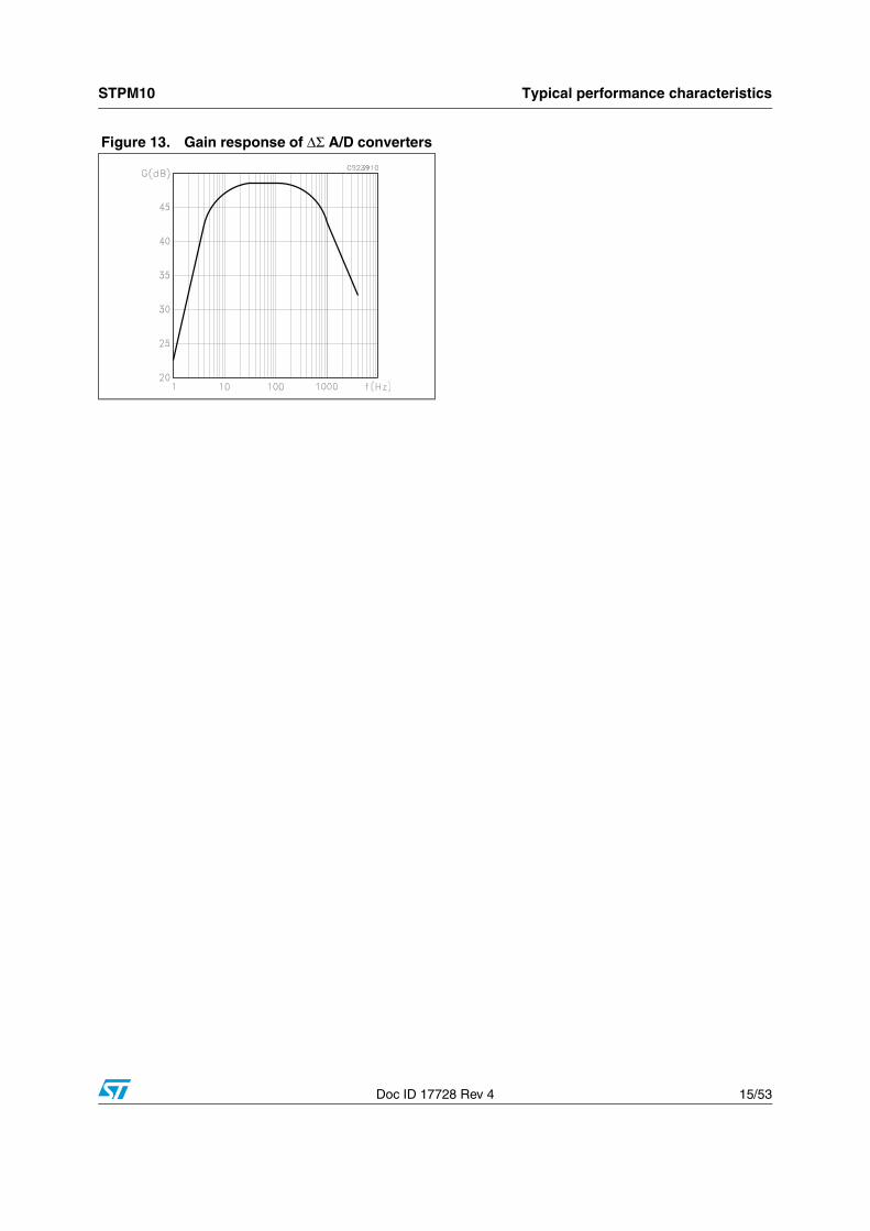
Figure 13. Gain response of ΔΣ A/D converters

Theory of operation STPM10
16/53 Doc ID 17728 Rev 4
7 Theory of operation
7.1 General operation descriptionThe STPM10 is capable of performing measurements of active, reactive and apparent energy, RMS and instantaneous voltage and current values, and line frequency information.
Most of the functions are fully programmable using internal configuration bits accessible through the SPI interface. The STPM10 works as a peripheral in microcontroller-based metering systems. The ZCR and WDG pins are used to provide zero-crossing and watch-dog information, and the SPI pins are used to communicate with the microcontroller.
The STPM10 includes volatile internal registers that hold the useful information for the metering system. Two kinds of active energy are available: wide-band active energy (AW) which includes all harmonic content (also called type 0) and fundamental active energy (AF), limited to the 1st harmonic (also called type 1). This latter energy value is obtained by filtering type 0 active energy. Both the two active energies are stored in up-down counting accumulator registers with a 20-bit length. Reactive and apparent energies are also available with a 20-bit accumulation.
The STPM10 also provides the RMS values for voltage and current. Due to the modest dynamic variation of the voltage, the RMS value is stored with a resolution of 11 bits, while the RMS current value has a resolution of 16 bits. The instantaneous (momentary) sampled value of voltage and current are also available with a resolution of 11 and 16 bits, respectively. The line frequency value is stored with a resolution of 14 bits.
Due to the proprietary energy computation algorithm, the STPM10 calibration is quick and simple, allowing calibration at only one point over the entire current range.
The configuration and calibration parameters must be downloaded in the internal non-volatile memory of STPM10 at power-up.
7.2 Analog inputs
Input amplifiers
The STPM10 has one fully differential voltage input channel and two fully differential current input channels.
The voltage channel consists of a differential amplifier with a gain of 4. The maximum differential input voltage for the voltage channel is ± 0.3 V.
The two current channels are multiplexed (see Section 7.9 for details) to provide a single input to a preamplifier with a gain of 4. The output of this preamplifier is connected to the input of a programmable gain amplifier (PGA) with possible gain selections of 2 and 8. The total gain of the current channels are then 8 and 32. The gain selections are made by writing to the gain register, and they can be different for the two current channels. If the tamper function is not used, the secondary current can be disabled.
The maximum differential input voltage is dependent on the selected gain, in accordance with Table 6.

STPM10 Theory of operation
Doc ID 17728 Rev 4 17/53
The gain register is included in the device configuration register with the address name PST. The table below shows the gain configuration according to the register values:
Note: If the device is used in configuration PST = 1, TMP = 1 (primary channel with CT, secondary channel with Shunt), the shunt Ks must always be equal to one fourth of the current transformer Ks.
Both the voltage and current channels implement an active offset correction architecture which provides the benefit of avoiding any offset compensation.The analog voltage and current signals are processed by the Σ Δ analog-to-digital converters, which feed the hard-wired DSP. The DSP implements an automatic digital offset cancellation that makes it possible to avoid any manual offset calibration on the analog inputs.
Table 6. Gain of voltage and current channels
Voltage channels Current channels
Gain Max input voltage (V) Gain Max input voltage (V)
4 ±0.308X ±0.15
32X ±0.035
Table 7. Configuration of current sensors
Primary SecondaryConfiguration
BitsConfiguration
Bits
Gain Sensor Gain Sensor PST TMP
8 CT Disabled Disabled 0 0
32 Shunt Disabled Disabled 1 0
8CT
8 CT 0 1
8 32 Shunt 1 1

Theory of operation STPM10
18/53 Doc ID 17728 Rev 4
7.3 ΣΔ A/D convertersAnalog-to-digital conversion in the STPM10 is carried out using two first-order Σ Δ converters. The device performs A/D conversions of analog signals on two independent channels in parallel. The current channel is multiplexed as a primary or secondary current channel in order to perform the tamper function, if enabled. The converted Σ Δ signals are supplied to the internal hard-wired DSP unit, which filters and integrates these signals in order to boost the resolution and to yield all the necessary signals for the computations.
A Σ Δ modulator converts the input signal into a continuous serial stream of 1’s and 0’s at a rate determined by the sampling clock. In the STPM10, the sampling clock is equal to fCLK/4.
The 1-bit DAC in the feedback loop is driven by the serial data stream. The DAC output is subtracted from the input signal. If the loop gain is high enough, the average value of the DAC output (and therefore the bit stream) can approach that of the input signal level. When a large number of samples are averaged, a very precise value for the analog signal is obtained. This averaging is carried out in the DSP section, which implements decimation, integration and DC offset cancellation of the supplied Σ Δ signals. The gain of the decimation filters is 1.004 for the voltage channel and 0.502 for the current channel. The resulting signal has a resolution of 11 bits per voltage channel and 16 bits per current channel.
Figure 14. First-order ΣΔ A/D converter
DAC
-
+
Integrator
fCLK/4
Input analog signal
Output digital signal
Σ ∫
STPM10 Theory of operation
Doc ID 17728 Rev 4 19/53
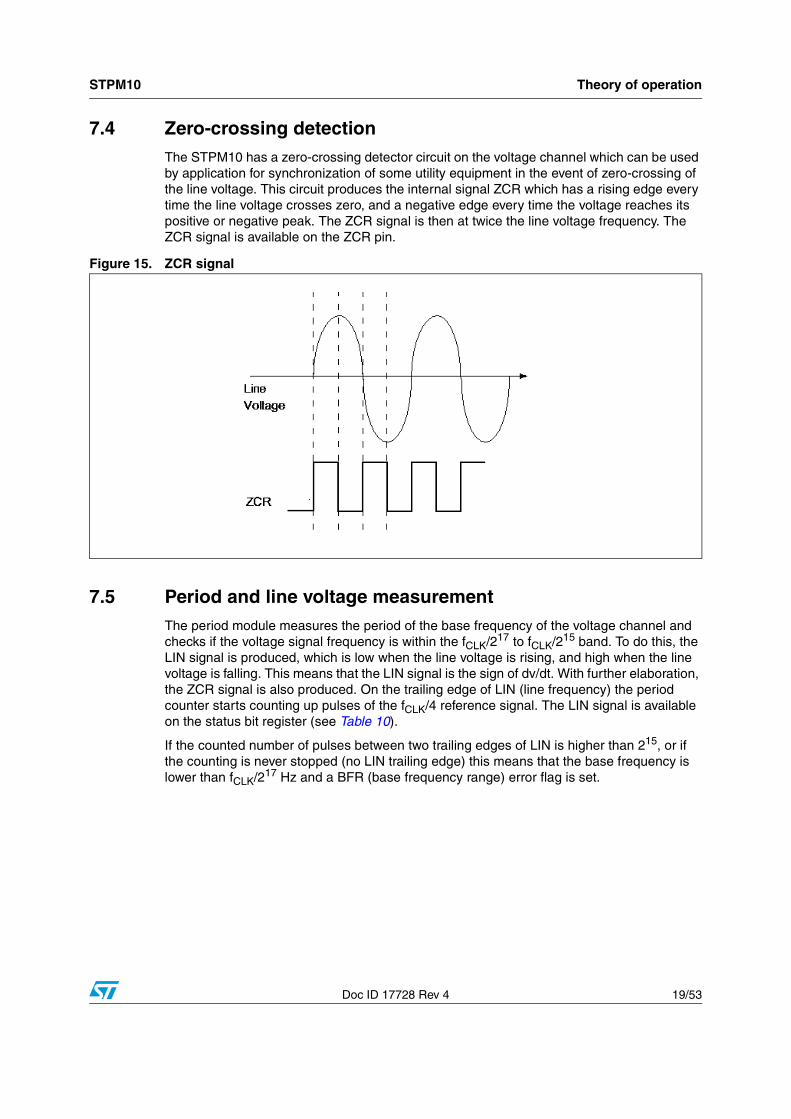
7.4 Zero-crossing detectionThe STPM10 has a zero-crossing detector circuit on the voltage channel which can be used by application for synchronization of some utility equipment in the event of zero-crossing of the line voltage. This circuit produces the internal signal ZCR which has a rising edge every time the line voltage crosses zero, and a negative edge every time the voltage reaches its positive or negative peak. The ZCR signal is then at twice the line voltage frequency. The ZCR signal is available on the ZCR pin.
7.5 Period and line voltage measurementThe period module measures the period of the base frequency of the voltage channel and checks if the voltage signal frequency is within the fCLK/217 to fCLK/215 band. To do this, the LIN signal is produced, which is low when the line voltage is rising, and high when the line voltage is falling. This means that the LIN signal is the sign of dv/dt. With further elaboration, the ZCR signal is also produced. On the trailing edge of LIN (line frequency) the period counter starts counting up pulses of the fCLK/4 reference signal. The LIN signal is available on the status bit register (see Table 10).
If the counted number of pulses between two trailing edges of LIN is higher than 215, or if the counting is never stopped (no LIN trailing edge) this means that the base frequency is lower than fCLK/217 Hz and a BFR (base frequency range) error flag is set.
Figure 15. ZCR signal

Theory of operation STPM10
20/53 Doc ID 17728 Rev 4
If the number of pulses counted between two trailing edges of LIN is lower than 213, the base frequency exceeds the limit (this means it is higher than fCLK/215). In this case, the error must be repeated three consecutive times in order to set the BFR error flag.
For example, with a 4.194304 MHz oscillator frequency and MDIV bit clear (or 8.192 MHz with MDIV set), fCLK/4 is 1.048576 MHz. If the line frequency is 30 Hz, the counted fCLK/4 pulses between two LIN trailing edges are 34952, more than 215 (32768 pulses).
The BFR low frequency limit is then:
fCLK/217 = 4194304/131072 = 32 Hz
With the same clock frequency, if the line frequency is 130 Hz, the fCLK/4 pulses between two LIN trailing edges are 8066, less than 213 (8192). The BFR high frequency limit is then:
fCLK/215 = 4194304/32768 = 128 Hz.
The BFR flag is also set if the register value of the RMS voltage drops below 64. BFR is cleared when the register value goes above 128. The BFR, then, also gives information about the presence of the line voltage within the meter.
When the BFR error is set, the computation of power is zero unless the FRS bit is set.
In fact, the effect of the BFR bit can be overridden by setting FRS configuration bit.
Figure 16. LIN and BFR signals
STPM10 Theory of operation
Doc ID 17728 Rev 4 21/53
It means that if FRS is set and BFR is also set, all the energy computation is carried on as BFR was cleared. In this case then p=u*i, where u could be zero or not (if BFR was set because voltage RMS register value is below 64).
When the line frequency re-enters the nominal band, the BFR flag is automatically reset. This BFR error flag is also assembled as part of the 8-bit status register (see Table 10).
7.6 Power supplyThe main STPM10 supply pin is the VCC pin. From the VCC pin two linear regulators provide the necessary voltage for the analog part VDDA (3 V) and for the digital part VDDD (1.8 V).
The VSS pin represents the reference point for all the internal signals. A 100 nF low ESR capacitor should be connected between VCC and VSS, VDDA and VSS, VDDD and VSS. All these capacitors must be located very close to the device.
The STPM10 contains a power on reset (POR) detection circuit. If the VCC supply is less than 2.5 V, then the STPM10 goes into an inactive state, all the functions are blocked and a reset condition is asserted. This is useful to ensure correct device operation at power-up and during power-down. The power supply monitor has built-in hysteresis and filtering, which give a high degree of immunity from false triggering due to noisy supplies.
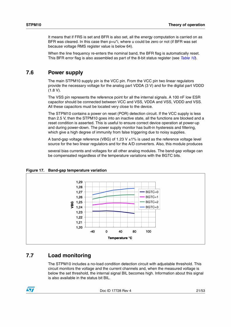
A band-gap voltage reference (VBG) of 1.23 V ±1% is used as the reference voltage level source for the two linear regulators and for the A/D converters. Also, this module produces
several bias currents and voltages for all other analog modules. The band-gap voltage can be compensated regardless of the temperature variations with the BGTC bits.
7.7 Load monitoringThe STPM10 includes a no-load condition detection circuit with adjustable threshold. This circuit monitors the voltage and the current channels and, when the measured voltage is below the set threshold, the internal signal BIL becomes high. Information about this signal is also available in the status bit BIL.
Figure 17. Band-gap temperature variation
1,20
1,21
1,22
1,23
1,24
1,25
1,26
1,27
1,28
1,29
-40 0 40 80
Temperature °C
VB
G
BGTC=0
BGTC=1
BGTC=2
BGTC=3
1001,20
1,21
1,22
1,23
1,24
1,25
1,26
1,27
1,28
1,29
-40 0 40 80
Temperature °C
VB
G
BGTC=0
BGTC=1
BGTC=2
BGTC=3
100
Theory of operation STPM10
22/53 Doc ID 17728 Rev 4
The no-load condition occurs when the product of the VRMS and IRMS register values is below a given value. This value can be set with the LTCH configuration bits. Four different no-load threshold values can be chosen according to the two configuration bits LTCH (see Table 8).
When a no-load condition occurs (BIL=1) the integration of power is suspended and the tamper module is disabled. The BIL signal can be accessed only through the SPI interface.
7.8 Error detectionIn addition to the no-load condition and the line frequency band, the integration of power can also be suspended due to an error detected on the source signals.
There are two kinds of error-detection circuits involved. The first checks all the Σ Δ signals from the analog part if any is stacked at 1 or 0 within the 1/128 of fCLK period of observation.
In case of a detected error, the corresponding Σ Δ signal is replaced with an idle Σ Δ signal, which represents a constant value of 0. All error and other resolved flags are treated as bits of a device status and can be read out by means of the SPI interface.
Another error condition occurs if LED pin output signals are different from the internal signals that drive them. This can occur if some of these pins are forced to GND or to some other imposed voltage value. In this case, the internal status bit PIN is activated, providing the information that some hardware problem has been detected.
7.9 Tamper detection moduleThe STPM10 is able to measure the current in both live and neutral wire with a time domain multiplexing approach on a unique sigma delta modulator. This mechanism is adopted to implement anti-tamper function. If this function is selected (see Table 7), the live and neutral wire currents are monitored; when the difference between the two measurements exceeds a rated threshold the STPM10 enters the "tamper state", while in "normal state" the two measurements are below the threshold.
In particular, both channels are not observed all the time, rather a time multiplex mechanism is used. During the observation time of each channel, its active energy is calculated. A tamper condition occurs when the absolute value of the difference between the two active energy values is greater than a certain percentage of the averaged energy during the activated tamper module (see Equation 1).
This percentage value can be selected between two different values (12.5 % and 6.25 %) according to the value of the configuration bit CRIT.
The tamper condition is detected when the following formula is satisfied:
Table 8. No-load detection thresholds
LTCH KLTCH
0 800
1 1600
2 3200
3 6400

STPM10 Theory of operation
Doc ID 17728 Rev 4 23/53
Equation 1
EnergyCH1 - EnergyCH2 > KCRIT (EnergyCH1 + EnergyCH2)/2;
where KCRIT can be 12.5 % or 6.25 %.
The detection threshold is much higher than the accuracy difference of the current channels, which should be less than 0.2 %, but, some headroom should be left for possible transition effect, due to accidental synchronism of actual load current change with the rhythm of taking the energy samples.
The tamper circuit works if the energies associated with the two current channels are both positive or negative, if the two energies have different sign, the tamper is on all the time however, the channel with the associated higher power is selected for the final computation of energy.
When internal signals are not good enough to perform the calculations, i.e. line period is out or range or ΔΣ signals from analog section are stacked at high or low logic level, or no load condition is activated, the tamper module is disabled and its state is preset to normal.
7.9.1 Detailed operational description
The meter is initially set to normal state, i.e. tamper not detected.In this condition the primary channel is selected for final integration of energy. In such state the values of both load currents should not differ more than the accuracy difference of the channels does. Sixty-four periods of line voltage is used as a tamper checking period.
After 24 periods of line voltage two internal signals MUX and INH are changed in order to enable secondary current channel and to freeze the last power and RMS values of primary current channel. The following 16 periods of line frequency are used for tamper detection integration. During this gap, the final energy calculation does not use the signal from selected channel but the frozen values.
Four line periods after the INH switch, the integration of power from secondary current channel is started and lasts four periods. Additional four line periods later MUX signal is switched back to primary current channel and the integration for tamper detection is started.
The timings of MUX and INH signals are shown in Figure 18 below.
Figure 18. Timings of tamper module - primary channel selected
MUX Ch 1 Ch 2 Ch 1 Ch 1
INH
Tamper power integrators B A
Cycles 4 4 4 424 24AM16596v1

Theory of operation STPM10
24/53 Doc ID 17728 Rev 4
When the secondary channel is selected to be integrated by the final energy integrator, the MUX and INH signals change according to Figure 19 below.
This means that energy of four periods from secondary channel followed by energy of four periods from primary channel is sampled within the tamper module. From these two samples, called B and A respectively, the criteria of tamper is calculated and the channel with higher current is selected, resulting in a new tamper state. If four consecutive new results of criteria happen, i.e. after elapsed 5.12 s at 50 Hz, the meter will enter into tamper state. Thus, the channel with the higher current will be selected for the energy calculation. If samples of power A and B would have different signs, the Tamper would be on all the time but, the channel with bigger power would be still selected for the final integration of energy.
If a tamper status has been detected, the multiplex ratio will be 56:8 if the primary channel energy is greater than the secondary one, otherwise it will be 8:56.
The detected tamper condition is stored in the BIT status bit. If BIT = 0 tamper is not detected, if BIT = 1 a tamper condition has been detected. In standalone mode the BIT flag is also available in the SDATD pin.
7.10 Phase compensationThe STPM10 does not introduce any phase shift between the voltage and current channel. However, the voltage and current signals come from transducers, which could have inherent phase errors. For example, a phase error of 0.1° to 0.3° is not uncommon for a current transformer (CT). These phase errors can vary from part to part, and they must be corrected in order to perform accurate power calculations. The errors associated with phase mismatch are particularly noticeable at low power factors. The STPM10 provides a means of digitally calibrating these small phase errors by introducing delays on the voltage or current signal. The amount of phase compensation can be set using the 4 bits of the phase calibration register (CPH).
The default value of this register is at a value of 0, which gives 0° phase compensation. When the 4 bits give a CPH of 15 (1111) the compensation introduced is +0.576°. This compensates the phase shift usually introduced by the current sensor, while the voltage sensor, normally a resistor divider, does not introduce any delay. The resolution step of the phase compensation is 0.038°.
Figure 19. Timings of tamper module - secondary channel selected

STPM10 Theory of operation
Doc ID 17728 Rev 4 25/53
7.11 Clock generatorAll the internal timing of the STPM10 is based on the CLKOUT signal. This signal can be generated in three different ways:
1. RC: this oscillator mode can be selected using the RC configuration bit. If RC = 1, the STPM10 runs using the RC oscillator. A resistor connected between CLKIN and ground sets the RC current. For 4 MHz operation, the recommended settling resistor is 12 kΩ. The oscillator frequency can be compensated using the CRC configuration bit.
2. Quartz: If RC = 0, the oscillator works with an external crystal. The recommended circuit is depicted in Figure 20 (b).
3. External clock: by keeping RC=0, it is also possible to feed the CLKOUT pin with an external oscillator signal.
The clock generator is powered from an analog supply and is responsible for two tasks. The first is to retard the turn-on of some function blocks after POR in order to help smooth the start of the external power supply circuitry by keeping off all major loads. The second task of the clock generator is to provide all necessary clocks for the analog and digital parts. During this task, the MDIV configuration bit is used to inform the device about the nominal frequency value of CLKOUT. Two nominal frequency ranges are expected to be from 4.000 MHz to 4.194 MHz (MDIV = 0) or from 8.000 MHz to 8.192 MHz (MDIV = 1).
7.11.1 RC startup procedure
To use the device with RC oscillator the configuration bit RC (see Table 11) must be set. Since the default configuration is for a crystal oscillator, when a RC oscillator is used instead and the device is supplied for the very first time it is not internally clocked and consequently the DSP is inactive. In this condition it is not possible to set RC or any other configuration bit.
The following SPI procedure can be run in order to set the RC bit and provide the clock to the device:
● Set the mode signal BANK;
● Perform a software reset;
● Read the registers: BANK mode signal should be checked and the records should show something (not 000000F0);
● Clear the mode signal BANK;
● DO NOT perform a reading, and write configuration bit RC;
Figure 20. Different oscillator circuits with (a) quartz, (b) internal oscillator, (c) external source
Theory of operation STPM10
26/53 Doc ID 17728 Rev 4
In this way the RC oscillator is started. If the registers are read again, it can be seen that RC bit is set and BANK is cleared. Once the RC startup procedure is complete, the device is clocked and active. For details on mode signals refer to Section 7.18, for SPI operations refer to Section 7.19.
7.12 Resetting the STPM10The STPM10 has no reset pin. The device is automatically reset by the POR circuit when the VCC crosses the 2.5 V value, but it can also be reset through the SPI interface by providing a dedicated command (see Section 7.19 for remote reset command details).
In case of reset caused by the POR circuit, all clocks and both DC buffers in the analog part are kept off for about 30 ms, as well as all blocks of the digital part, except for the SPI interface, which is held in a reset state for about 125 ms after a reset condition.
When a reset is performed through SPI, no delayed turn-on is generated.
Resetting the STPM10 causes all the functional modules of the STPM10 to be cleared, including the volatile memory.
The reset through SPI (remote reset request) normally takes place during production testing.
7.13 Using the STPM10 in microcontroller-based metersThe STPM10 can be used in microcontroller-based energy meters.
The SPI pins (SCS, SCL, SDA, SYN) are used for communication purposes, allowing the microcontroller to write and read the internal STPM10 registers.
The zero-crossing signal is available at the ZCR pin (see Section 7.4 for details about the ZCR signal).
The WDG pin provides the watchdog signal (DOG). The DOG signal generates a 16 ms long positive pulse every 1.6 seconds. Generation of these pulses can be suspended if data are read in intervals shorter than 1.6 s. The DOG signal is actually a watchdog reset signal which can be used to control operation of an on-board microcontroller. It is set to high whenever the VDDA voltage is below 2.5 V, but after VDDA goes above 2.5 V this signal starts running.
It is expected that an application microcontroller should access the data in the metering device on a regular basis at least 1/s (recommended is 32/s). Every latching of results in the metering device requested from the microcontroller also resets the watchdog. If latching requests are not 1.6 seconds from one another, an active high pulse on WDG is produced, because the device assumes that the microcontroller is not operating properly. An application can use this signal either to control the reset pin of its microcontroller, or it can be tied to an interrupt pin. The latter option is recommended for a battery-backup application which can enter a sleep mode due to power-down conditions, and should not be reset by a metering device as it would exit from sleep mode.

STPM10 Theory of operation
Doc ID 17728 Rev 4 27/53
7.14 Energy to frequency conversionThe STPM10 provides energy to frequency conversion both for calibration and energy readout purposes. In fact, one convenient way to verify the meter calibration is to provide a pulse train signal with 50% duty cycle whose frequency signal is proportional to the active energy under steady load conditions. In this case, the user chooses a certain number of pulses on the LED pin that correspond to 1 kWh. This value is called P.
Let us consider the case in which the LED pin is configured to be driven from internal signal AW (active energy) whose frequency is proportional to the active energy. The signal AW is taken from the 11th bit of the active energy register, and consequently a relationship between the LSB value of the active energy register and the number of pulses provided per each kWh (P) can be defined as:
Equation 2
Due to the innovative and proprietary power calculation algorithm, the frequency signal is not affected by any ripple at twice the line frequency. This feature strongly reduces the calibration time of the meter.
In a practical example where the desired P is 64000 pulses/kWh (=17.7 Hz*kW), we have:
Equation 3
kAW=7.63*10-6 Wh
This means that the reading of 0x00001 in the active energy register represents 7.63 µWh, while 0xFFFFF represents 8 Wh.
The LED pin can be driven from AW (active energy wide band), AF (active energy limited at fundamental), RW (reactive energy) or SW (apparent energy) according to the value of the KMOT bit.
In this case, since the LED pin is driven by signals different from that of AW, some other relationship between the LSB of the register and the number of pulses per kWh provided by the meter (P) must be defined:
Equation 4
kAF = 4*kAW [Wh]
kRW = 2*kAW [VARh]
kSW = kAW [VAh]
Table 9. LED pin configuration
KMOT (2 bits) Signal available on LED pin # of pulses
0 AW Type0* P [kWh]
1 AF Type1* P [kWh]
2 RW P [kVARh]
3 SW P [kVAh]
KAW1000
211 P⋅-------------------- Wh[ ]=

Theory of operation STPM10
28/53 Doc ID 17728 Rev 4
7.15 Status bitsThe STPM10 includes 8 status bits which provide information about the current status of the meter. The status bits are the following:
All these signal can be read through the SPI interface. See Section 7.15: Status bits for details on the status bit location in the STPM10 data records.
Table 10. Status bit description
Bit # Name Description Condition
0 BIL No-load conditionBIL = 0: No-load condition not detected
BIL = 1: No-load condition detected
1 BCF Σ Δ signals statusBCF = 0: Σ Δ signals active
BCF = 1: One or both Σ Δ signals are stacked
2 BFR Line frequency rangeBFR = 0: Line frequency within the 45 Hz - 65 Hz range
BFR = 1: Line frequency out of range
3 BIT Tamper conditionBIT = 0: Tamper not detected
BIT = 1: Tamper detected
4 MUX Current channel selection
MUX = 0: Primary current channels selected by the tamper module
MUX = 1: Secondary current channels selected by the tamper module
5 LIN Trend of the line voltage
LIN = 0: Line voltage going from the minimum to the maximum value. (dv/dt > 0)
LIN = 1: Line voltage going from the maximum to the minimum value. (dv/dt < 0)
6 PIN Output pin check
PIN = 0: Output pins are consistent with the data
PIN = 1: Output pins are different with the data, this means an output pin is forced to 1 or 0
7 HLT Data validity
HLT = 0: Data records reading are valid.
HLT = 1: Data records are not valid. A reset occurred and a restart is in progress

STPM10 Theory of operation
Doc ID 17728 Rev 4 29/53
7.16 Programming the STPM10
7.16.1 Data records
The STPM10 has 8 internal data record registers. Every data record consists of a 4-bit parity code and 28-bit data value where the parity code is computed from the data value, which makes a total of 32 bits, or 4 bytes.
Figure 21 shows the data record structure with the name of the contained information. Each bit of parity nibble is defined as odd parity of all seven corresponding bits of data nibbles.
The first 6 registers are read-only, except for the 8-bit mode signals in the DFP register (the mode signals are described later in this paragraph). The last two registers are CFL and CFH.
7.17 Configuration bitsAll the configuration bits that control the operation of the device (CFL and CFH data records) can be written in a temporary way. The configuration bit values are written in the so-called volatile memory, which are simple latches that hold the configuration data until the power is on or until a reset condition occurs (both POR and remote reset).
As indicated in the data records table, the configuration bits are 56.
Figure 21. STPM10 data record map
upper f(u)0 1
mode signals
p
p
iRMSuRMS
iMOMuMOM
1bit1bit 1bit
20 bit20 bit 8 bit
6 bit
11 bit 16 bit
DAP
DRP
DSP
CFH
DFP
DEV
DMV
CFL
reactive energy
type0 active energy
apparent energy
type 1 energy
lower part of configurators
upper part of configurators
Status
lower f(u)
parity
parity
parity
parity
parity
parity
parity
parity
4 bit
msb lsb

Theory of operation STPM10
30/53 Doc ID 17728 Rev 4
Each configuration bit can be written by sending a byte command to STPM10 through its SPI interface. The procedure to write the configuration bits is described in Section 7.19: SPI interface.
Table 11. Configuration bit map
Address
Namen. of bits
Description (1)6-bit
binaryDEC
000000 0 - 1 Reserved
000001 1 MDIV 1Measurement frequency range selection:- MDIV=0: 4.000 MHz to 4.194 MHz - MDIV=1: 8.000 MHz to 8.192 MHz
000010 2 RC 1Type of internal oscillator selection:- RC=0:crystal oscillator,- RC=1:RC oscillator
000011 3 - 1 Reserved
000100 4 - 1 Reserved
000101 5 PST 1
Current channel sensor type and gain:If TMP=0PST=0: primary is CT x8, secondary is not used, no tamperPST=1: primary is shunt x32, secondary is not used, no tamper
If TMP=1PST=0: primary is CT x8, secondary is CT x8, tamperPST=1: primary is CT x8, secondary is shunt x32, tamper
000110 6 - 1 Reserved
000111 7 TMP 1 Tamper enable
001000 8 FRS 1Power calculation when BFR=1 - FRS=0: energy accumulation is frozen, power is set to zero;- FRS=1: normal energy accumulation and power computation (p=u*i);
001001 9 MSBF 1Bit sequence output during record data reading selection:- MSBF=0: MSB first - MSBF=1: LSB first
001010 10 FUND 1
This bit swaps the information stored in the type0 (first 20 bits of DAP register) and type1 (first 20 bits of DFP register) active energy.- FUND = 0: type 0 contains wide-band active energy, type1 contains fundamental active energy- FUND = 1: type 0 contains fundamental active energy, type1 contains wide- band active energy
001100 12
LTCH 2
No-load condition threshold as product between VRMS and IRMS:LTCH=0 800LTCH=1 1600LTCH=2 3200LTCH=3 6400
001101 13 (1)

STPM10 Theory of operation
Doc ID 17728 Rev 4 31/53
001110 14
KMOT 2
Selection of pulses for LED:KMOT=0 Type 0 Active EnergyKMOT=1 Type 1 Active EnergyKMOT=2 Reactive EnergyKMOT=3 Apparent Energy
001111 15 (1)
010000 16 - 1 Reserved
1 Reserved010001 17 -
010010 18BGTC 2 Band-gap temperature compensation bits. See Figure 17 for details.
010011 19 (1)
010100 20
CPH 44-bit unsigned data for compensation of phase error, 0°+0.576°.16 values are possible with a compensation step of 0.0384°. When CPH=0 the compensation is 0°, when CPH=15 the compensation is 0.576°.
010101 21
010110 22
010111 23 (1)
011000 24
CHV 8
8-bit unsigned data for voltage channel calibration.256 values are possible. When CHV is 0 the calibrator is at -12.5% of the nominal value. When CHV is 255 the calibrator is at +12.5%. The calibration step is then 0.098%.
011001 25
011010 26
011011 27
011100 28
011101 29
011110 30
011111 31 (1)
100000 32
CHP 8
8-bit unsigned data for primary current channel calibration.256 values are possible. When CHP is 0 the calibrator is at -12.5% of the nominal value. When CHP is 255 the calibrator is at +12.5%. The calibration step is then 0.098%.
100001 33
100010 34
100011 35
100100 36
100101 37
100110 38
100111 39 (1)
Table 11. Configuration bit map (continued)
Address
Namen. of bits
Description (1)6-bit
binaryDEC

Theory of operation STPM10
32/53 Doc ID 17728 Rev 4
As indicated above, the STPM10 includes 56 CFG bits. The CFG bits are not retained when the STPM10 supply is not available and they are cleared when a POR occurs, but they are not cleared when a remote reset command (RRR) is sent through SPI.
Normally, some of these bits must be loaded during power-up of the application. From the microcontroller, it could also reload the configuration and calibration values after power-on restart.
101000 40
CHS 8
8-bit unsigned data for secondary current channel calibration.256 values are possible. When CHS is 0 the calibrator is at -12.5% of the nominal value. When CHS is 255 the calibrator is at +12.5%. The calibration step is then 0.098%.
101001 41
101010 42
101011 43
101100 44
101101 45
101110 46
101111 47 (1)
110000 48
CRC 2
2-bit unsigned data for calibration of RC oscillator. (see Table 5)CRC=0, or CRC=3 cal=0%CRC=1, cal=+10%;CRC=2, cal=-10%.
110001 49 (1)
110010 50 - 1 Reserved
110011 51 - 1 Reserved
110100 52 - 1 Reserved
110101 53 CRIT 1Selection of tamper threshold:CRIT=0: 12,5% / CRIT=1: 6,25%
110110 54 - 1 Reserved
110111 55 - 1 Reserved
1. IMPORTANT: This bit represents the MSB of the decimal value indicated in the description column.
Table 11. Configuration bit map (continued)
Address
Namen. of bits
Description (1)6-bit
binaryDEC
STPM10 Theory of operation
Doc ID 17728 Rev 4 33/53
7.18 Mode signalsThe STPM10 includes 8 mode signals located in the DFP data record. 3 of these are used only for internal testing purposes while 5 are useful to change some of the operations of the STPM10. The mode signals are not retained when the STPM10 supply is not available and they are cleared when a POR occurs, but they are not cleared when a remote reset command (RRR) is sent through SPI.
The mode signals bit can be written using the normal writing procedure of the SPI interface (see Section 7.19).
– CSEL: In normal operation, if the anti-tamper module is not activated (see PST configuration bits) the STPM10 selects channel 1 as the source of current information. For debug or calibration purposes it is possible to select channel 2 as the source of the current channel signal when the tamper module is disabled. This is done by setting the CSEL mode bit.
– Precharge: This command swaps the sequence of data records read, allowing the reading of the last four data records first, and the first four second. The reading sequence is 5, 6, 7, 8, 1, 2, 3, 4. Unlike the other mode signals, the precharge command is not retained inside the STPM10, but should be sent each time before the reading of the data records.
– BANK: it is used to activate RC oscillator (see Section 7.11.1).–––––
Table 12. Mode signal description
Bit #Signal name
Bit value
StatusBinary
commandHex
command
0 BANK0
Used for RC startup procedure0111000x 70 or 71
1 1111000x F0 or F1
1 Reserved
2 Reserved
3 Reserved
4 CSEL0 Current channel 1 selected when tamper is disabled 0111 100x 78 or 79
1 Current channel 2 selected when tamper is disabled 1111 100x F8 or F9
5 Reserved
6 Reserved
7 Precharge 1Swap the 32-bit data record readings. From 1,2,3,4,5,6,7,8, to 5,6,7,8,1,2,3,4 and vice-versa
1111111x FF

Theory of operation STPM10
34/53 Doc ID 17728 Rev 4
7.19 SPI interfaceThe SPI interface supports a simple serial protocol, which is implemented to enable communication between some master system (microcontroller or PC) and the device.
Three tasks can be performed with this interface:
– remote resetting of the device
– reading data records
– writing the mode bits and the configuration bits
Four pins of the device are dedicated to this purpose: SCS, SYN, SCL and SDA.
SCS, SYN and SCL are all input pins, while SDA can be input or output according to whether the SPI is in write or read mode. A high-level signal for these pins means a voltage level higher than 0.75 x VCC, while a low-level signal means a voltage value lower than 0.25 x VCC.
The internal registers are not directly accessible. Instead, 32 bits of transmission latches are used to pre-load the data before being read or written to the internal registers.
The condition in which SCS, SYN and SCL inputs are set to high level determines the idle state of the SPI interface, and no data transfer occurs.
– SCS: enables SPI operation when low.
– SYN: operates different functions according to the status of the SCS pin. When SCS is low, the SYN pin status selects if the SPI is in read (SYN = 1) or write mode (SYN = 0). When the SCS is high and SYN is also high, the results of the input or output data are transferred to the transmission latches.
– SCL: basically the clock pin of the SPI interface. This pin function is also controlled by the SCS status. If SCS is low, SCL is the input of the serial bit synchronization clock signal. When SCS is high, SCL is also high, determining the idle state of the SPI.
– SDA: the data pin. If SCS is low, the operation of SDA is dependent on the status of the SYN pin. If SYN is high, SDA is the output of the serial bit data (read mode). If SYN is low, SDA is the input of the serial bit data signal (write mode). If SCS is high, SDA is the input of the idle signal.
Any pin above has an internal weak pull-up mechanism of nominal 15 µA. This means that when a pin is not forced by external signals, the state of the pin is logic high. A high state of any input pin described above is considered an idle (not active) state. For the SPI to operate correctly, the STPM10 must be correctly supplied as described in Section 7.6: Power supply. An idle state of the SPI module is recognized when the signals of pins SYN, SCS, SCL and SDA are in a logic high state. Any SPI operation should start from this idle state.
When SCS is active (low), signal SDATD should change its state at trailing edge of signal SCLNLC and the signal SDATD should be stable at next leading edge of signal SCLNLC. The first valid bit of SDATD is always started with activation of signal SCLNLC.

STPM10 Theory of operation
Doc ID 17728 Rev 4 35/53
7.20 Remote resetThe timing diagram of this operation is shown in Figure 22. The time step can be as short as 30 ns.
The internal reset signal is called RRR. Unlike the POR, the RRR signal does not cause the 30 ms delayed restart of the analog module, and the 120 ms delay in the restart of the digital module. This signal does not clear the mode signals.
7.21 Reading data recordsA microcontroller is able to read all measurement results and all system signals (configuration, calibration, status, mode). Again, the time step can be as short as 30 ns. There are two phases of reading, called latching and shifting.
Latching is used to sample results into transmission latches. The transmission latches are the flip-flops that hold the data in the SPI interface. This is done with the active pulse on SYN when SCS is idle. The length of the pulse on SYN must be longer than 2 periods of the measurement clock, i.e. more than 500 ns at 4 MHz.
The shifting starts when SCS become active. In the beginning of this phase, another much shorter pulse (30 ns) on SYN should be applied in order to ensure that an internal transmission serial clock counter is reset to zero. An alternative way is to extend the pulse on SYN into the second phase of reading. After this reset is done, a 32 serial clocks-per-data record should be applied. Up to 8 data records can be read this way. This procedure can be aborted at any time through deactivation of SCS (see Figure 24).
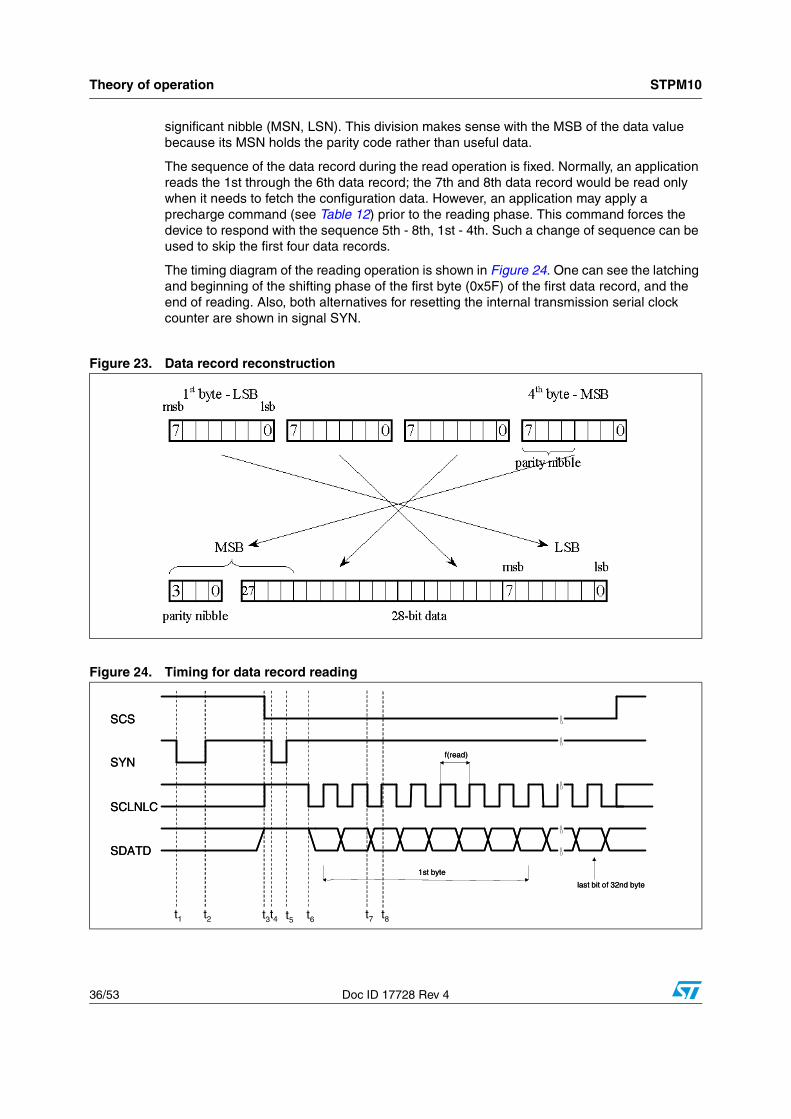
The first read-out byte of the data record is the least significant byte (LSB) of the data value and, of course, the fourth byte is the most significant byte (MSB) of the data value. Each byte can be further divided into a pair of 4-bit nibbles, referred to as the most and least
Figure 22. Timing for providing remote reset request (1)
1. All time intervals must be longer than 30 ns. t7 → t8 is the reset time; this interval must be longer than 30 ns also.
t1 t2 t3 t4 t5 t6 t7 t8 t9 t10
SCS
SYN
SCLNLC
SDATD
SCS
SYN
SCLNLC
SDATD
Theory of operation STPM10
36/53 Doc ID 17728 Rev 4
significant nibble (MSN, LSN). This division makes sense with the MSB of the data value because its MSN holds the parity code rather than useful data.
The sequence of the data record during the read operation is fixed. Normally, an application reads the 1st through the 6th data record; the 7th and 8th data record would be read only when it needs to fetch the configuration data. However, an application may apply a precharge command (see Table 12) prior to the reading phase. This command forces the device to respond with the sequence 5th - 8th, 1st - 4th. Such a change of sequence can be used to skip the first four data records.
The timing diagram of the reading operation is shown in Figure 24. One can see the latching and beginning of the shifting phase of the first byte (0x5F) of the first data record, and the end of reading. Also, both alternatives for resetting the internal transmission serial clock counter are shown in signal SYN.
Figure 23. Data record reconstruction
Figure 24. Timing for data record reading
t1 t2 t3t4 t5 t6 t7 t8
SCLNLC
SDATD
SYN
SCS
1st byte
last bit of 32nd byte
f(read)
SCLNLC
SDATD
SYN
SCS
1st byte
last bit of 32nd byte
f(read)
STPM10 Theory of operation
Doc ID 17728 Rev 4 37/53
t1 → t2: Latching phase. Interval value > 2/fCLK
t2 → t3: Data latched, SPI idle. Interval value > 30 ns
t3 → t4: Enable SPI for read operation. Interval value > 30 ns
t4 → t5: Serial clock counter is reset. Interval value > 30 ns
t5 → t6: SPI reset and enabled for read operation. Interval value > 30 ns
t7: Internal data transferred to SDA
t8: SDA data is stable and can be read
The system that reads the data record from the STPM10 should check the integrity of each data record. If the check fails, the reading should be repeated, but this time only the shifting should be applied. Otherwise, new data would be latched into transmission latches and the one incorrectly read would be lost.
Normally, each byte is read out as the most significant bit (MSB) first. But this can be changed by setting the MSBF configuration bit in the STPM10 CFL data record. If this is done, each byte is read out as the least significant bit (LSB) first.
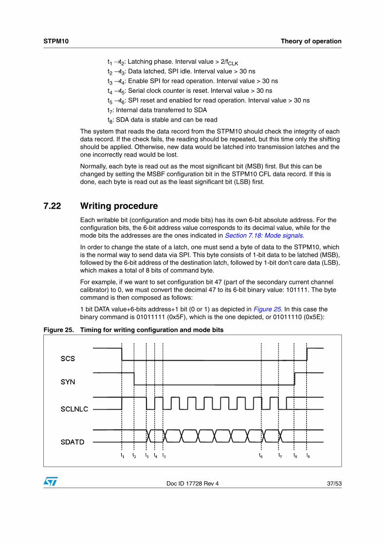
7.22 Writing procedureEach writable bit (configuration and mode bits) has its own 6-bit absolute address. For the configuration bits, the 6-bit address value corresponds to its decimal value, while for the mode bits the addresses are the ones indicated in Section 7.18: Mode signals.
In order to change the state of a latch, one must send a byte of data to the STPM10, which is the normal way to send data via SPI. This byte consists of 1-bit data to be latched (MSB), followed by the 6-bit address of the destination latch, followed by 1-bit don't care data (LSB), which makes a total of 8 bits of command byte.
For example, if we want to set configuration bit 47 (part of the secondary current channel calibrator) to 0, we must convert the decimal 47 to its 6-bit binary value: 101111. The byte command is then composed as follows:
1 bit DATA value+6-bits address+1 bit (0 or 1) as depicted in Figure 25. In this case the binary command is 01011111 (0x5F), which is the one depicted, or 01011110 (0x5E):
Figure 25. Timing for writing configuration and mode bits
Theory of operation STPM10
38/53 Doc ID 17728 Rev 4
t1 → t2 (> 30 ns): SPI out of idle state
t2 → t3 (> 30 ns): SPI enabled for write operation
t3: data value is placed in SDA
t4: SDA value is stable and shifted into the device
t3 → t5 (> 10 µs): writing clock period
t3 → t5: 1 bit data value
t5 → t6: 6 bit address of the destination latch
t6 → t7: 1 bit EXE command
t8: end of SPI writing
t9: SPI enters idle state
The same procedure should be applied for the mode signals, but in this case the 6-bit address must be taken from Table 12.
The LSB of the command is also called the EXE bit because instead of the data bit value, the corresponding serial clock pulse is used to generate the necessary latching signal. This way the writing mechanism does not need the measurement clock in order to operate, which makes the operation of SPI module of STPM10 completely independent from the rest of device logic except for the signal POR.
Commands for changing system signals should be sent during active signals SCS and SYN, as shown in Figure 25. The SYN must be put low in order to disable the SDA output driver of the STPM10 and make the SDA an input pin. A string of commands can be sent within one period of active SCS and SYN signals, or a command can be followed by reading the data record. However, in this case, the SYN should be deactivated in order to enable the SDA output driver, and a SYN pulse should be applied before activation of the SCS in order to latch the data.
7.22.1 Interfacing the standard 3-wire SPI with the STPM10 SPI
Due to the fact that a 2-wire SPI is implemented in the STPM10, it is clear that sending any command from a standard 3-wire SPI would require a 3-wire to 2-wire interface, which should produce a proper signal on SDA from host signals SDI, SDO and SYN. The need for a single-gate 3-state buffer could be avoided through an emulation of SPI just to send some commands. On a microcontroller this would be done by performing the following steps:
1. Disable the SPI module
2. Set the SDI pin, which is connected to SDA as an output
3. Activate SYN first, and then SCS
4. Apply a new bit value to SDI, and activate SCL
5. Deactivate SCL
6. Repeat the previous two steps seven times to complete a one byte transfer
7. Repeat the previous three steps for any remaining byte transfers
8. Set the SDI pin as an input
9. Deactivate SCS and SYN
10. Enable the SPI module

STPM10 Theory of operation
Doc ID 17728 Rev 4 39/53
In case of a precharge command (0xFF), the emulation above is not necessary. Due to the pull-up device on the SDA pin of the STPM10, the processor needs to perform the following steps:
1. Activate SYN first in order to latch the results
2. After at least 1 µs, activate SCS
3. Write one byte to the transmitter of SPI (this produces 8 pulses on SCL with SDI=1)
4. Deactivate SYN
5. Optionally read the data records (the sequence of reading is altered)
6. Deactivate SCS
7.23 Energy calculation algorithmWithin the STPM10, the computing section of the measured active power uses a completely new patented signal processing approach. This approach allows the device to reach high a level of performance in terms of accuracy.
The signals, coming from the sensors, for the instantaneous voltage are calculated as follows:
Equation 5
v(t) = V•sin ωt
where V is the peak voltage and ω is related to the line frequency.
The instantaneous current is calculated using:
Equation 6
i(t) = I • sin (ωt + ϕ)
where I is the peak current, ω is related to the line frequency and ϕ is the phase difference between voltage and current.
7.23.1 Active power
In the STPM10, after the pre-conditioning and the A/D conversion, the digital voltage signal (which is dynamically more stable with respect to the current signal) is processed by a differentiator stage which transforms:
Equation 7
v(t) → v’(t) = dv/dt = V ⋅ ω ⋅ cos ωt − [see Figure 26 - 5]
the resulting signal, together with the pre-processed and digitalized current signal:
Equation 8
i(t) = I ⋅ sin(ωt + ϕ); [see Figure 26 - 6]
are then available for the calculation process. These digital signals are also provided to two additional stages, which then integrate of themselves, obtaining:

Theory of operation STPM10
40/53 Doc ID 17728 Rev 4
Equation 9
dv/dt → v(t) = V ⋅ sin ωt; [see Figure 26 - 7]
Equation 10
i(t) →
[see Figure 26 - 8]
At this point four signals are available. By combining (pairing) them by means of two multiplying stages, two results are obtained:
Equation 11
[see Figure 26 - 9]
I t( ) i∫ t( ) dtIω-- wt ϕ+( )cos⋅–=⋅=
Figure 26. Active energy computation diagram
p1 t( )dv
dt----- i∫ t( ) dt⋅ ⋅ V I ϕcos⋅ ⋅
2--------------------------------- V I 2wt ϕ+( )cos⋅ ⋅
2-------------------------------------------------------––= =
STPM10 Theory of operation
Doc ID 17728 Rev 4 41/53
Equation 12
[see Figure 26 - 10]
After these two operations, another stage performs the subtraction between the results p2 and p1 and a division by 2, obtaining the active power:
Equation 13
[see Figure 26 - 11]
In this way, the AC part V•I•cos(2ωt + ϕ)/2 has been removed from the instantaneous power.
The absence of any AC component allows for a very fast calibration procedure. It requires only the setting of (using the internal device programming registers) the voltage and current sensor conversion constants, using the effective voltage and current (Vrms, Irms) readings provided by the device’s built-in communication port, avoiding the time-averaged readings of the active power or the need for line synchronization.
7.23.2 Reactive power
The reactive power is produced using the previously-computed signals. In case of shunt sensor the voltage signal is derived while the current signal is not. A first computation is to multiply the DS value of the integrated voltage channel with the value of the integrated current channel, which yields:
Equation 14
The second is to multiply the filtered DS value of the voltage channel with the value of the filtered current channel:
Equation 15
From the above results, Q1(t) is proportional to 1/ω, while Q2(t) is proportional to ω. The correct reactive power would result from the following formula:
p2 t( ) v t( ) i t( )⋅ V I ϕcos⋅ ⋅2
--------------------------------- V I 2wt ϕ+( )cos⋅ ⋅2
-------------------------------------------------------––= =
p t( )p2 t( ) p1 t( )–( )
2------------------------------------ V I ϕcos⋅ ⋅
2---------------------------------= =
Q1 t( ) v t( )dt I⋅ t( ) v t( ) I t( )⋅= V ωtsin( ) Iω-- ωt ϕ+( )cos–⎝ ⎠
⎛ ⎞ VI2ω------ ϕsin 2ωt ϕ+( )sin–( )⋅=⋅=∫=
Q2 t( ) v t( ) I⋅ t( ) vω ωtcos I⋅= ωt ϕ+( )sinVI2------ ω ϕsin((⋅ 2ωt ϕ+( ) )sin+⋅==
Theory of operation STPM10
42/53 Doc ID 17728 Rev 4
Equation 16
Since the above computation would need significant additional circuitry, the reactive power in the STPM10 is calculated using only the Q1(t) multiplied by ω, which means:
Equation 17
The reactive power, then, presents a ripple at twice the line frequency. Since the average value of a sinusoid is 0, this ripple does not contribute to the reactive energy calculation over time. Moreover, in the STPM10 the reactive power is not used for meter calibration or to generate the stepper pulses, so this ripple does not affect the overall system performance.
7.23.3 Apparent power and RMS values
The RMS values are calculated starting from the following formulas:
Equation 18
Multiplying Equation 18 by ω , the IRMS value is obtained:
Equation 19
The RMS voltage value is obtained by:
Equation 20
Q12--- Q1 t( ) ω Q2 t( ) 1
ω---
VI2------ ϕsin=⋅+⋅ ⋅=
Q3 t( ) 12--- Q1 t( ) ω VI
2------ ϕsin 2ωt ϕ+( )sin–( )⋅=⋅ ⋅=
1T--- I2 t( ) td
0
T
∫ I
ω 2⋅-----------------=
IRMSI
2-------=
VRMS1T--- v2 t( ) td
0
T
∫ V
2-------= =
STPM10 Theory of operation
Doc ID 17728 Rev 4 43/53
For the apparent power, another value is produced:
Equation 21
Multiplying Equation 18 and Equation 21, the apparent power is produced:
Equation 22
The DSP then performs the integration of the computed powers into energies. These integrators are implemented as up/down counters and they can roll over. 20-bit output buses of the counters are assigned as the most significant part of the energy data records. It is the responsibility of an application to read the counters at least every second, to avoid missing any rollover.
7.24 STPM10 calibrationEnergy meters based on the STPM10 device can be calibrated in a fast and simple way. The calibration is essentially based on the single calibration of the voltage and current channel considering their RMS values rather than on the frequency of the output pulse signal. When the two channels are calibrated, all the other measurements are calibrated too. This allows the calibration to be performed in only one point, thereby shortening the production time of the meter.
This procedure is possible due to the following key factors:
● The device comprises two independent meter channels for line voltage and current, respectively. Each channel includes its own digital calibrator, to adjust the RMS in the range of ±12.5% in 256 steps, and a digital filter, to remove any signal DC component. None of the final results are subject to the calibration procedure because they are achieved from such corrected signals by mathematical modules implemented by hard-wired DSP.
● The device computes different kinds of energies: active, reactive and apparent. The active energy is produced without the 2nd harmonic of the line frequency. It also computes RMS values of measured voltage and current.
● The device produces an energy output pulse signal, but information can also be read through the serial port interface (SPI) and communication channel.
● The device has an embedded memory of 56 bits, used for configuration and calibration purposes. The values of these bits can be read, or they can be changed temporarily through the SPI communication channel.
1T--- v2 t( ) td
0
T
∫ V ω⋅2
--------------=
SI
ω 2⋅----------------- V ω⋅
2-------------- VI
2------=⋅=
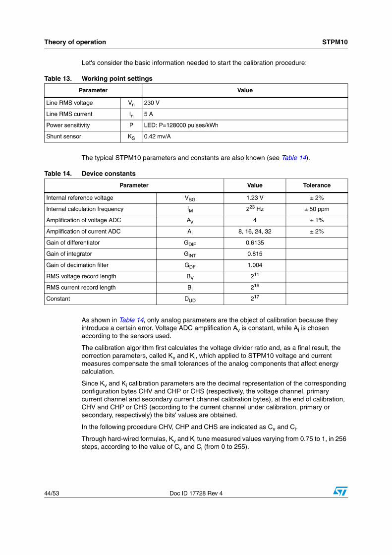
Theory of operation STPM10
44/53 Doc ID 17728 Rev 4
Let's consider the basic information needed to start the calibration procedure:
The typical STPM10 parameters and constants are also known (see Table 14).
As shown in Table 14, only analog parameters are the object of calibration because they introduce a certain error. Voltage ADC amplification Av is constant, while Ai is chosen according to the sensors used.
The calibration algorithm first calculates the voltage divider ratio and, as a final result, the correction parameters, called Kv and Ki, which applied to STPM10 voltage and current measures compensate the small tolerances of the analog components that affect energy calculation.
Since Kv and Ki calibration parameters are the decimal representation of the corresponding configuration bytes CHV and CHP or CHS (respectively, the voltage channel, primary current channel and secondary current channel calibration bytes), at the end of calibration, CHV and CHP or CHS (according to the current channel under calibration, primary or secondary, respectively) the bits' values are obtained.
In the following procedure CHV, CHP and CHS are indicated as Cv and Ci.
Through hard-wired formulas, Kv and Ki tune measured values varying from 0.75 to 1, in 256 steps, according to the value of Cv and Ci (from 0 to 255).
Table 13. Working point settings
Parameter Value
Line RMS voltage Vn 230 V
Line RMS current In 5 A
Power sensitivity P LED: P=128000 pulses/kWh
Shunt sensor KS 0.42 mv/A
Table 14. Device constants
Parameter Value Tolerance
Internal reference voltage VBG 1.23 V ± 2%
Internal calculation frequency fM 223 Hz ± 50 ppm
Amplification of voltage ADC AV 4 ± 1%
Amplification of current ADC AI 8, 16, 24, 32 ± 2%
Gain of differentiator GDIF 0.6135
Gain of integrator GINT 0.815
Gain of decimation filter GDF 1.004
RMS voltage record length BV 211
RMS current record length BI 216
Constant DUD 217
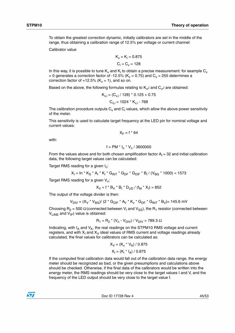
STPM10 Theory of operation
Doc ID 17728 Rev 4 45/53
To obtain the greatest correction dynamic, initially calibrators are set in the middle of the range, thus obtaining a calibration range of 12.5% per voltage or current channel:
Calibrator value
Kv = Ki = 0.875
Ci = Cv = 128
In this way, it is possible to tune Kv and Ki to obtain a precise measurement: for example Cv = 0 generates a correction factor of -12.5% (Kv = 0.75) and Cv = 255 determines a correction factor of +12.5% (Kv = 1), and so on.
Based on the above, the following formulas relating to Kv,i and Cv,i are obtained:
Kv,i = (Cv,i / 128) * 0.125 + 0.75
Cv,i = 1024 * Kv,i - 768
The calibration procedure outputs Cv and Ci values, which allow the above power sensitivity of the meter.
This sensitivity is used to calculate target frequency at the LED pin for nominal voltage and current values:
XF = f * 64
with:
f = PM * In * Vn / 3600000
From the values above and for both chosen amplification factor AI = 32 and initial calibration data, the following target values can be calculated:
Target RMS reading for a given In:
XI = In * KS * AI * Ki * GINT * GDF * GDIF * BI / (VBG * 1000) = 1573
Target RMS reading for a given Vn:
XV = f * BV * BI * DUD / (fM * XI) = 852
The output of the voltage divider is then:
VDIV = (XV * VBG)/ (2 * GDIF * AV * Kv * GDF * GINT * BV)= 145.6 mV
Choosing R2 = 500 Ω (connected between VI and VSS), the R1 resistor (connected between VLINE and VIP) value is obtained:
R1 = R2 * (Vn - VDIV) / VDIV = 789.3 Ω
Indicating, with IA and VA, the real readings on the STPM10 RMS voltage and current registers, and with XI and XV ideal values of RMS current and voltage readings already calculated, the final values for calibrators can be calculated as:
XV = (Kv * VA) / 0.875
XI = (Ki * IA) / 0.875
If the computed final calibration data would fall out of the calibration data range, the energy meter should be recognized as bad, or the given presumptions and calculations above should be checked. Otherwise, if the final data of the calibrators would be written into the energy meter, the RMS readings should be very close to the target values I and V, and the frequency of the LED output should be very close to the target value f.

Application design STPM10
46/53 Doc ID 17728 Rev 4
8 Application design
The choice of the external components in the transduction section of the application is a crucial point in the application design, affecting the precision and the resolution of the whole system.
Among the several considerations, a compromise has to be found between the following needs:
1. Maximize the signal to noise ratio in the voltage channel,
2. Choose the current to voltage conversion ratio Ks and the voltage divider ratio in a way that calibration can be achieved (please refer to AN2299)
3. Choose Ks to take advantage of the whole current dynamic range according to desired maximum current and resolution.
To maximize the signal to noise ratio of the current channel the voltage divider resistors ratio should be as close as possible to those shown in Table 15.
The Figure 27 below shows a reference schematic for an application with the following properties:
● P = 64000 imp/kWh
● INOM = 5 A
● IMAX = 60 A.
Typical values for the current sensors sensitivity, also used in the reference schematic below, are shown in Table 16.
Note: If the device is used in configuration PST = 1, TMP = 1 (primary channel with CT, secondary channel with Shunt), the shunt Ks must always be equal to one fourth of the current transformer Ks.
Additional considerations on the application design, suggestions for noise and crosstalk reduction can be found in the AN2317.
Table 15. Resistor divider ratio
Function Component Parameter Value Unit
Line voltage interface Resistor dividerR to R ratio VRMS=230V 1650
V/VR to R ratio VRMS=110V 830
Table 16. Current channel typical components
Function Component Parameter Value Unit
Line current interface
Current shunt
Current to voltage conversion ratio Ks
0.425
mV/ACurrent transformer 1.7
Rogowsky coil 0.13
STPM10 Application design
Doc ID 17728 Rev 4 47/53
Figure 27. STPM10 reference schematic with one current transformer and one shunt

Package mechanical data STPM10
48/53 Doc ID 17728 Rev 4
9 Package mechanical data
In order to meet environmental requirements, ST offers these devices in different grades of ECOPACK® packages, depending on their level of environmental compliance. ECOPACK® specifications, grade definitions and product status are available at: www.st.com. ECOPACK® is an ST trademark.

STPM10 Package mechanical data
Doc ID 17728 Rev 4 49/53
Dim.mm. inch.
Min. Typ. Max. Min. Typ. Max.
A 1.2 0.047
A1 0.05 0.15 0.002 0.004 0.006
A2 0.8 1 1.05 0.031 0.039 0.041
b 0.19 0.30 0.007 0.012
c 0.09 0.20 0.004 0.0079
D 6.4 6.5 6.6 0.252 0.256 0.260
E 6.2 6.4 6.6 0.244 0.252 0.260
E1 4.3 4.4 4.48 0.169 0.173 0.176
e 0.65 BSC 0.0256 BSC
K 0° 8° 0° 8°
L 0.45 0.60 0.75 0.018 0.024 0.030
TSSOP20 mechanical data
c Eb
A2A
E1
D
1PIN 1 IDENTIFICATION
A1LK
e
0087225C
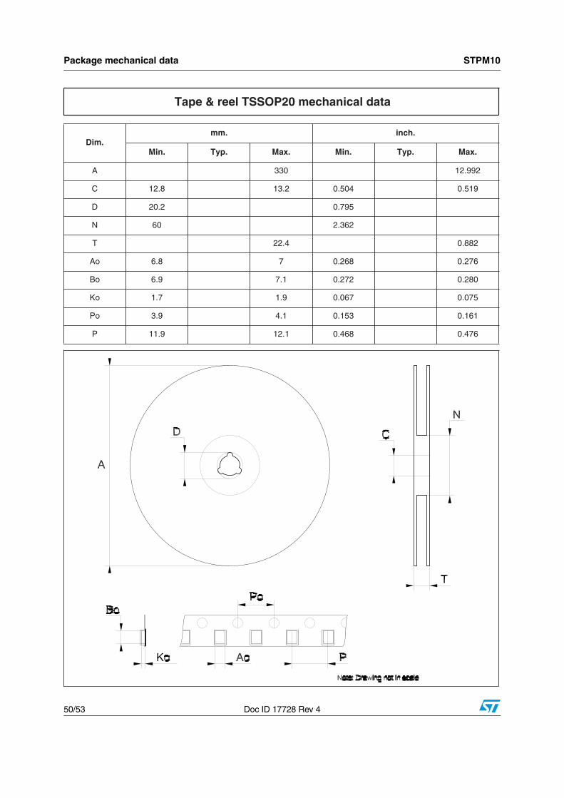
Package mechanical data STPM10
50/53 Doc ID 17728 Rev 4
Dim.mm. inch.
Min. Typ. Max. Min. Typ. Max.
A 330 12.992
C 12.8 13.2 0.504 0.519
D 20.2 0.795
N 60 2.362
T 22.4 0.882
Ao 6.8 7 0.268 0.276
Bo 6.9 7.1 0.272 0.280
Ko 1.7 1.9 0.067 0.075
Po 3.9 4.1 0.153 0.161
P 11.9 12.1 0.468 0.476
Tape & reel TSSOP20 mechanical data
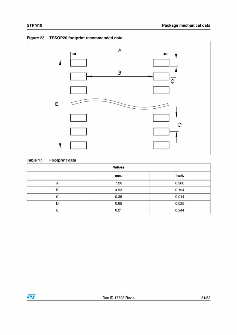
STPM10 Package mechanical data
Doc ID 17728 Rev 4 51/53
Figure 28. TSSOP20 footprint recommended data
Table 17. Footprint data
Values
mm. inch.
A 7.26 0.286
B 4.93 0.194
C 0.36 0.014
D 0.65 0.025
E 6.21 0.244
Revision history STPM10
52/53 Doc ID 17728 Rev 4
10 Revision history
Table 18. Document revision history
Date Revision Changes
31-Aug-2010 1 Initial release.
25-Nov-2010 2Modified: Table 5 on page 9, 7.9: Tamper detection module on page 22.Added: 7.11.1: RC startup procedure on page 25 and 8: Application design on page 46.
09-Jun-2011 3 Updated Table 5.
29-Jan-2013 4 Updated Table 9.
STPM10
Doc ID 17728 Rev 4 53/53
Please Read Carefully:
Information in this document is provided solely in connection with ST products. STMicroelectronics NV and its subsidiaries (“ST”) reserve theright to make changes, corrections, modifications or improvements, to this document, and the products and services described herein at anytime, without notice.
All ST products are sold pursuant to ST’s terms and conditions of sale.
Purchasers are solely responsible for the choice, selection and use of the ST products and services described herein, and ST assumes noliability whatsoever relating to the choice, selection or use of the ST products and services described herein.
No license, express or implied, by estoppel or otherwise, to any intellectual property rights is granted under this document. If any part of thisdocument refers to any third party products or services it shall not be deemed a license grant by ST for the use of such third party productsor services, or any intellectual property contained therein or considered as a warranty covering the use in any manner whatsoever of suchthird party products or services or any intellectual property contained therein.
UNLESS OTHERWISE SET FORTH IN ST’S TERMS AND CONDITIONS OF SALE ST DISCLAIMS ANY EXPRESS OR IMPLIEDWARRANTY WITH RESPECT TO THE USE AND/OR SALE OF ST PRODUCTS INCLUDING WITHOUT LIMITATION IMPLIEDWARRANTIES OF MERCHANTABILITY, FITNESS FOR A PARTICULAR PURPOSE (AND THEIR EQUIVALENTS UNDER THE LAWSOF ANY JURISDICTION), OR INFRINGEMENT OF ANY PATENT, COPYRIGHT OR OTHER INTELLECTUAL PROPERTY RIGHT.
UNLESS EXPRESSLY APPROVED IN WRITING BY TWO AUTHORIZED ST REPRESENTATIVES, ST PRODUCTS ARE NOTRECOMMENDED, AUTHORIZED OR WARRANTED FOR USE IN MILITARY, AIR CRAFT, SPACE, LIFE SAVING, OR LIFE SUSTAININGAPPLICATIONS, NOR IN PRODUCTS OR SYSTEMS WHERE FAILURE OR MALFUNCTION MAY RESULT IN PERSONAL INJURY,DEATH, OR SEVERE PROPERTY OR ENVIRONMENTAL DAMAGE. ST PRODUCTS WHICH ARE NOT SPECIFIED AS "AUTOMOTIVEGRADE" MAY ONLY BE USED IN AUTOMOTIVE APPLICATIONS AT USER’S OWN RISK.
Resale of ST products with provisions different from the statements and/or technical features set forth in this document shall immediately voidany warranty granted by ST for the ST product or service described herein and shall not create or extend in any manner whatsoever, anyliability of ST.
ST and the ST logo are trademarks or registered trademarks of ST in various countries.
Information in this document supersedes and replaces all information previously supplied.
The ST logo is a registered trademark of STMicroelectronics. All other names are the property of their respective owners.
© 2013 STMicroelectronics - All rights reserved
STMicroelectronics group of companies
Australia - Belgium - Brazil - Canada - China - Czech Republic - Finland - France - Germany - Hong Kong - India - Israel - Italy - Japan - Malaysia - Malta - Morocco - Philippines - Singapore - Spain - Sweden - Switzerland - United Kingdom - United States of America
www.st.com