programmer’s reference manual - versalogic.com · programming information for hardware interfaces...
TRANSCRIPT

Programmer’s Reference Manual DOC. REV. 12/09/2015
Fox (VL-EPM-19) DMP Vortex86DX2 SoC-based SBC with dual Ethernet, Video, USB, SATA, Counter/Timers, Mini PCIe, microSD, GPIO, SPX, and PC/104-Plus Interface

EPM-19 Programmer’s Reference Manual ii
WWW.VERSALOGIC.COM
12100 SW Tualatin Road Tualatin, OR 97062-7341
(503) 747-2261 Fax (971) 224-4708
Copyright © 2015 VersaLogic Corp. All rights reserved.
Notice: Although every effort has been made to ensure this document is error-free, VersaLogic makes no representations or warranties with respect to this product and specifically disclaims any implied warranties of merchantability or fitness for any particular purpose.
VersaLogic reserves the right to revise this product and associated documentation at any time without obligation to notify anyone of such changes.
PC/104 and the PC/104 logo are trademarks of the PC/104 Consortium.

EPM-19 Programmer’s Reference Manual iii
Product Release Notes Release 1 First release of this document.
Support The EPM-19 support page, at http://www.versalogic.com/private/foxsupport.asp contains additional information and resources for this product including:
Reference Manual (PDF format)
Operating system information and software drivers
VersaAPI Version 1.2.0 and later
Data sheets and manufacturers’ links for chips used in this product
BIOS information and upgrades
Utility routines and benchmark software
This is a private page for EPM-19 users that can be accessed only be entering this address directly. It cannot be reached from the VersaLogic homepage.
The VersaTech KnowledgeBase is an invaluable resource for resolving technical issues with your VersaLogic product.
VersaTech KnowledgeBase
EPM-19 Programmer’s Reference Manual iv
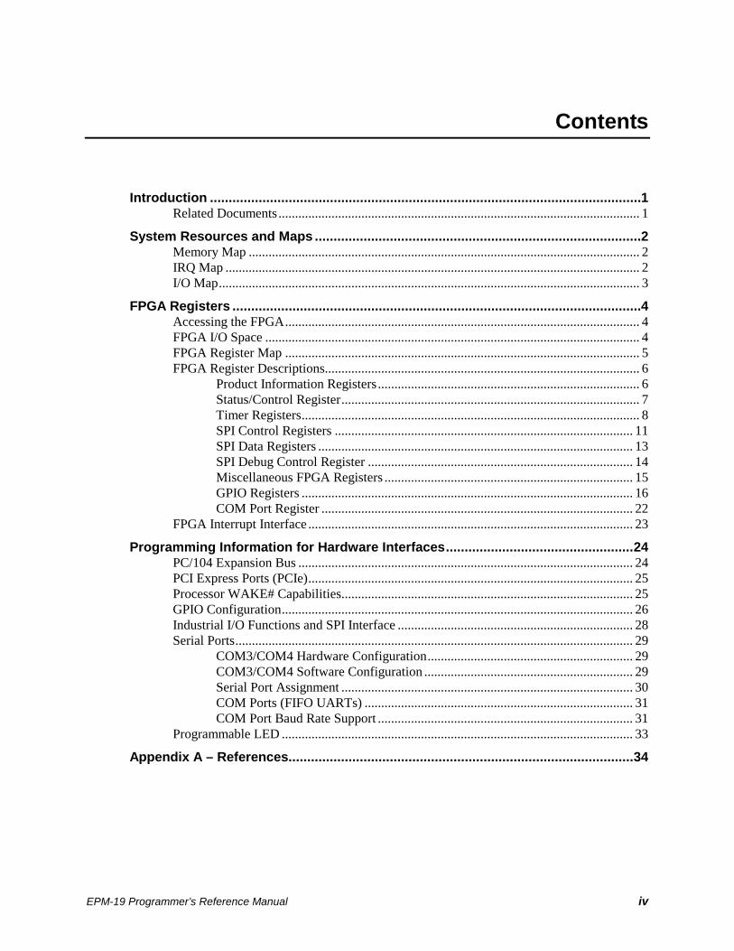
Contents
Introduction ................................................................................................................... 1 Related Documents ............................................................................................................. 1
System Resources and Maps ....................................................................................... 2 Memory Map ...................................................................................................................... 2 IRQ Map ............................................................................................................................. 2 I/O Map ............................................................................................................................... 3
FPGA Registers ............................................................................................................. 4 Accessing the FPGA ........................................................................................................... 4 FPGA I/O Space ................................................................................................................. 4 FPGA Register Map ........................................................................................................... 5 FPGA Register Descriptions............................................................................................... 6
Product Information Registers ............................................................................... 6 Status/Control Register .......................................................................................... 7 Timer Registers ...................................................................................................... 8 SPI Control Registers .......................................................................................... 11 SPI Data Registers ............................................................................................... 13 SPI Debug Control Register ................................................................................ 14 Miscellaneous FPGA Registers ........................................................................... 15 GPIO Registers .................................................................................................... 16 COM Port Register .............................................................................................. 22
FPGA Interrupt Interface .................................................................................................. 23
Programming Information for Hardware Interfaces .................................................. 24 PC/104 Expansion Bus ..................................................................................................... 24 PCI Express Ports (PCIe) .................................................................................................. 25 Processor WAKE# Capabilities........................................................................................ 25 GPIO Configuration .......................................................................................................... 26 Industrial I/O Functions and SPI Interface ....................................................................... 28 Serial Ports ........................................................................................................................ 29
COM3/COM4 Hardware Configuration .............................................................. 29 COM3/COM4 Software Configuration ............................................................... 29 Serial Port Assignment ........................................................................................ 30 COM Ports (FIFO UARTs) ................................................................................. 31 COM Port Baud Rate Support ............................................................................. 31
Programmable LED .......................................................................................................... 33
Appendix A – References............................................................................................ 34

Contents
EPM-19 Programmer’s Reference Manual v
Tables
Table 1: Memory Map ........................................................................................................ 2 Table 2: IRQ Map ............................................................................................................... 2 Table 3: I/O Map ................................................................................................................. 3 Table 4: FPGA I/O Map ...................................................................................................... 4 Table 5: FPGA Register Map.............................................................................................. 5 Table 6: PCR – Product Code and LED Register ............................................................... 6 Table 7: PSR – Product Status Register .............................................................................. 6 Table 8: SCR –Status/Control Register .............................................................................. 7 Table 9: TICR – 8254 Timer Interrupt Control Register .................................................... 8 Table 10: TISR – 8254 Timer Interrupt Status Register ..................................................... 9 Table 11: TCR – 8254 Timer Control Register ................................................................ 10 Table 12: SPI Control Register ......................................................................................... 11 Table 13: SPI Status Register............................................................................................ 12 Table 14: SPI – SPI Debug Control Register .................................................................... 14 Table 15: MISCR1 – Misc. Control Register #1 .............................................................. 15 Table 16: MISCSR2 – Misc. Control Register #2 ............................................................ 15 Table 17: AUXDIR – Auxiliary GPIO Direction Control Register .................................. 16 Table 18: AUXPOL – Auxiliary GPIO Polarity Control Register .................................... 17 Table 19: AUXOUT – Auxiliary GPIO I/O Output Value Register ................................. 18 Table 20: AUXIN – Auxiliary GPIO Input Value Register .............................................. 19 Table 21: AUXIMASK – Auxiliary GPIO I/O Interrupt Mask and Control Register ...... 20 Table 22: AUXISTAT– Auxiliary GPIO I/O Interrupt Mask and Status Register ........... 21 Table 23: AUXIMODE1– Auxiliary GPIO I/O Mode Register ....................................... 22 Table 24: COMMODE – COM Port Mode Control Register ........................................... 22 Table 25: PC/104 ISA I/O, IRQ, and Memory Resources ................................................ 24 Table 26: PCIe Port Configuration ................................................................................... 25 Table 27: Vortex86DX2 GPIO Configuration .................................................................. 26 Table 28: GPIO Port 2 Direction Register – 0x9A ........................................................... 30 Table 29: GPIO Port 2 Data Register – 0x7A ................................................................... 30 Table 30: Recommended Serial Port Settings for Vortex86DX2 BIOS ........................... 30 Table 31: COM Port PCI Address Map ............................................................................ 32 Table 32: Baud Rates, Divisors, and Base Clock and Ratio Selection for UARTs .......... 33
EPM-19 Programmer’s Reference Manual 1
Introduction
This document provides information for users requiring register-level information for developing applications with the EPM-19.
Related Documents The following documents available are on the EPM-19 Product Support Web Page:
EPM-19 Hardware Reference Manual – provides information on the board’s hardware features including connectors and all interfaces.
EPM-19_EBX-18 BIOS Reference Manual – provides information on accessing and configuring settings in the BIOS Setup utility. All BIOS menus, submenus, and configuration options are described.
VersaAPI Installation and Reference Guide – describes the shared library of API calls for reading and controlling on-board devices on certain VersaLogic products.
1

EPM-19 Programmer’s Reference Manual 2
System Resources and Maps
Memory Map Table 1: Memory Map
Address Range Description 00000000 – 0009FFFF System RAM 000A0000 – 000AFFFF EGA/VGA video memory 000B0000 – 000B7FFF MDA RAM, Hercules graphics display RAM 000B8000 – 000BFFFF CGA display RAM 000C0000 – 000C7FFF EGA/VGA BIOS ROM 000C8000 – 000CFFFF Boot ROM enable 000CC000 – 000CFFFF Console redirection enable 000D0000 – 000D7FFF Expansion ROM space 000D8000 – 000DBFFF SPI Flash emulation floppy A enable 000DC000 – 000DFFFF Expansion ROM space 000E0000 – 000EFFFF USB Legacy SCSI ROM space 000F0000 – 000FFFFF Motherboard BIOS FEFBB400 – FEFBB4FF On-board Ethernet adapter FEFDB800 – FEFDBFFF Standard enhanced PCI-to-USB host controller FEFDBC00 – FEFDBCFF Standard OpenHCD USB host controller
IRQ Map Table 2: IRQ Map
IRQ Description IRQ0 System timer IRQ1 Keyboard controller IRQ2 Cascade for IRQ8 – IRQ15 IRQ3 COM3 / Vortex86DX2 UART2 IRQ4 COM1 / Vortex86DX2 UART1 IRQ5 USB IRQ6 USB IRQ7 USB/Ethernet 10/100Mbit LAN IRQ8 Real-time clock IRQ9 Multimedia device
IRQ10 COM2 / Vortex86DX2 UART9 IRQ11 COM4 / Vortex86DX2 UART4 IRQ12 Mouse IRQ13 Math coprocessor IRQ14 Hard disk controller #1 IRQ15 Hard disk controller #2
2

System Resources and Maps
EPM-19 Programmer’s Reference Manual 3
I/O Map Table 3: I/O Map
I/O Address Range Device/Owner 0000h – 000Fh DMA 8237-1 0020h – 0021h 8259-1 programmable interrupt controller 0022h – 0023h Indirect access registers (6117D configuration port) 002Eh – 002Fh Forward to LPC bus 0040h – 0043h 8254 timer/counter 0048h – 004Bh 8254 counter (Reserved) 004Eh – 004Fh Forward to LPC bus 0060h Keyboard/Mouse data port 0061h Port B + NMI control port 0062h – 0063h 8051 download 4K address counter 0064h Keyboard/mouse command/status port 0065h Watchdog0 reload counter 0066h 8051 download 8-bit data port 0067h Watchdog1 reload counter 0068h – 006Dh Watchdog1 control counter 0070h – 0071h CMOS RAM port 0072h – 0075h MTBF control register 0078h – 007Ch GPIO port 0/1/2/3/4 default setup 0080h – 008Fh DMA page register 0092h System control register 0098h – 009Ch GPIO direction control 00A0h – 00A1h 8259-2 programmable interrupt controller 00C0h – 00DFh DMA 8237-2 00E0h – 00EFh DOS 4G page access 0170h – 0177h IDE1 (IRQ15) 01F0h – 01F7h IDE0 (IRQ14) 02E8h – 02EFh COM4 (IRQ11) 02F8h – 02FFh COM2 (IRQ10) 0376h IDE1 ATAPI device control write only register 03E8h – 03EFh COM3 (IRQ3) 03F6h IDE0 ATAPI device control write only register 03F8h – 03FFh COM1 (IRQ4) 0480h – 048Fh DMA high page register 0490h – 0499h Instruction counter register 04D0h – 04D1h 8259 Edge/level control register 0CF8h – 0CFFh PCI configuration port DE00h – DEFFh On-board LAN FC00h – FC05h SPI Flash BIOS control register FC08h – FC0Dh External SPI bus control register

EPM-19 Programmer’s Reference Manual 4
FPGA Registers
Accessing the FPGA To access the FPGA, obtain the PCI Base Address Register value (BAR) and add it to the Offset Address provided in Table 5 below. The PCI BAR can be obtained by reading the 32-bit hexadecimal value (indicated by the 0x prefix) loaded in the PCI Configuration register at address 0x10 for PCI Bus 02, Dev 04, Func 00.
The FPGA 32-bit PCI Configuration BAR would normally be read as 0x0000C801 (the LSB=1 simply enables I/O space and is not used with the base address calculation) if there are no other PCI expansion cards plugged into the system (including PCIe Minicards) which equates to the FPGA I/O Base Address at 0xC800. Add the Offset Address (found in column 1 of Table 5) to obtain the I/O address for each 8-bit register.
Example:
FPGA I/O Base Address 0xC800 SPICONTROL offset address + 0x08
I/O address for accessing the SPICONTROL register = 0xC808
FPGA I/O Space The FPGA is mapped into I/O space on the PCI bus. Without any PCI expansion cards (PC/104-Plus) in use, the FPGA is the only endpoint device on the PCI bus. The address range will be mapped into the I/O Space, but because this is a PCI-based device, the base address is subject to change with the use of PCIe or PCI expansion card use; therefore, it should be read each power cycle for use in calculating the FPGA register addresses.
FPGA access: PCI I/O space
FPGA access size: All 8-bit (single byte) I/O accesses
FPGA Address Range: PCI I/O BAR for Bus 02/Device 04/Function 00 added to offset range of 0x00 to 0x3FF (1 Kbyte window, but only addresses 0x00 to 0xFF contain utilized registers).
The three 8254 timers only require four bytes of addressing and are located at the end of the 256-byte I/O block. The only requirement is that the base address must be aligned on a 4-byte block. Table 4 lists the FPGA’s I/O map.
Table 4: FPGA I/O Map
Offset Address Range Device Size 0x00 – 0xFB FPGA registers 252 bytes 0xFC – 0xFF 8254 timer address registers 4 bytes
3

FPGA Registers
EPM-19 Programmer’s Reference Manual 5
FPGA Register Map Register Access Key
R/W Read/Write
RO Read-only (status or reserved)
R/WC Read-status/Write-1-to-Clear
WO Write-only (0 if read)
RSVD Reserved (registers implemented but not used)
Table 5: FPGA Register Map
Offset Address Identifier D7 D6 D5 D4 D3 D2 D1 D0
0x00 PCR PLED EPM-19 PRODUCT_CODE = 0010010
0x01 PSR REV_LEVEL RSVD 0 0
0x02 SCR 0 0 0 DEBUG_LED RSVD 0 0 0
0x03 TICR RSVD RSVD RSVD RSVD 0 IMSK_TC5 IMSK_TC4 IMSK_TC3
0x04 TISR INTRTEST TMRTEST TMRIN4 TMRIN3 0 ISTAT_TC5 ISTAT_TC4 ISTAT_TC3
0x05 TCR TIM5GATE TIM4GATE TIM3GATE TM45MODE TM4CLKSEL TM3CLKSEL TMROCTST TMRFULL
0x06 Reserved 0 0 0 0 0 0 0 0
0x07 Reserved 0 0 0 0 0 0 0 0
0x08 SPICONTROL CPOL CPHA SPILEN1 SPILEN0 MAN_SS SS2 SS1 SS0
0x09 SPISTATUS RSVD RSVD SPICLK1 SPICLK0 HW_IRQ_EN LSBIT_1ST HW_INT BUSY
0x0A SPIDATA0 MSB LSB
0x0B SPIDATA1 MSB LSB
0x0C SPIDATA2 MSB LSB
0x0D SPIDATA3 MSB LSB
0x0E SPI 0 MUXSEL2 MUXSEL1 MUXSEL0 0 0 SPILB 0
0x0F MISCSR1 0 0 0 0 0 0 0 0
0x11 MISCSR2 NO_BATT W_DISABLE 0 PBRST 0 0 0 USB_OBDIS
0x21 AUXDIR DIR_GPIO8 DIR_GPIO7 DIR_GPIO6 DIR_GPIO5 DIR_GPIO4 DIR_GPIO3 DIR_GPIO2 DIR_GPIO1
0x22 AUXPOL POL_GPIO8 POL_GPIO7 POL_GPIO6 POL_GPIO5 POL_GPIO4 POL_GPIO3 POL_GPIO2 POL_GPIO1
0x23 AUXOUT OUT_GPIO8 OUT_GPIO7 OUT_GPIO6 OUT_GPIO5 OUT_GPIO4 OUT_GPIO3 OUT_GPIO2 OUT_GPIO1
0x24 AUXIN IN_GPIO8 IN_GPIO7 IN_GPIO6 IN_GPIO5 IN_GPIO4 IN_GPIO3 IN_GPIO2 IN_GPIO1
0x25 AUXIMASK IMASK_ GPIO8
IMASK_ PIO7
IMASK_ GPIO6
IMASK_ GPIO5
IMASK_ GPIO4
IMASK_ GPIO3
IMASK_ GPIO2
IMASK_ GPIO1
0x26 AUXISTAT ISTAT_ GPIO8
ISTAT_ PIO7
ISTAT_ GPIO6
ISTAT_ GPIO5
ISTAT_ GPIO4
ISTAT_ GPIO3
ISTAT_ GPIO2
ISTAT_ GPIO1
0x27 AUXMODE1 MODE_ GPIO8
MODE_ PIO7
MODE_ GPIO6
MODE_ GPIO5
MODE_ GPIO4
MODE_ GPIO3
MODE_ GPIO2
MODE_ GPIO1
0x40 COMMODE 0 0 0 0 COM4_TXEN COM3_TXEN 0 0
0xFC 8254 Timer Address 0 MSB ————— —————— ————— ————— LSB
0xFD 8254 Timer Address 1 MSB ————— —————— ————— ————— LSB
0xFE 8254 Timer Address 2 MSB ————— —————— ————— ————— LSB
0xFF 8254 Timer Address 3 MSB ————— —————— ————— ————— LSB

FPGA Registers
EPM-19 Programmer’s Reference Manual 6
FPGA Register Descriptions Register Access Key
R/W Read/Write
RO Read-only (status or reserved)
R/WC Read-status/Write-1-to-Clear
WO Write-only (0 if read)
RSVD Reserved (registers implemented but not used)
PRODUCT INFORMATION REGISTERS The FPGA register at offset 0x00 (PCR VersaReg) provides read access to the product code. At offset 0x01 (PSR VersaReg), the revision level can be read.
Table 6: PCR – Product Code and LED Register
Bit Identifier Access Default Description
7 PLED R/W 0 Drives the programmable LED on the paddleboard. 0 – LED is off (default) 1 – LED is on (can be used by software)
6-0 PRODUCT_CODE RO 0010010 Product Code for the EPM-19 (0x12)
Table 7: PSR – Product Status Register
Bit Identifier Access Default Description
7:3 REV_LEVEL[4:0] RO N/A
Revision level of the PLD (incremented every FPGA release) 0 – Indicates production release revision level when BETA status bit (bit 0) is set to ‘0’ 1 – Indicates development release revision level when BETA status bit (bit 0) is set to ‘1’
2 Reserved RO 1 Reserved. Writes are ignored; reads always return 1.
1 Reserved RO 0 Reserved. Writes are ignored; reads always return 0.
0 Reserved RO 0 Reserved. Writes are ignored; reads always return 0.

FPGA Registers
EPM-19 Programmer’s Reference Manual 7
STATUS/CONTROL REGISTER
Table 8: SCR –Status/Control Register
Bit Identifier Access Default Description
7 Reserved RO N/A Reserved. Writes are ignored; reads always return 0.
6 Reserved RO N/A Reserved. Writes are ignored; reads always return 0.
5 Reserved RO N/A Reserved. Writes are ignored; reads always return 0.
4 DEBUG_LED R/W 1 Debug LED (controls the blue LED): 0 – LED is off and follows its primary function (MSATA_DAS) 1 – LED is on (indicates FPGA is programmed by default)
3 Reserved RSVD N/A Reserved. Writes are ignored; reads always return 0.
2 Reserved RO N/A Reserved. Writes are ignored; reads always return 0.
1 Reserved RO N/A Reserved. Writes are ignored; reads always return 0.
0 Reserved RO N/A Reserved. Writes are ignored; reads always return 0.

FPGA Registers
EPM-19 Programmer’s Reference Manual 8
TIMER REGISTERS The FPGA implements an 8254-compatible timer/counter that includes three 16-bit timers. Timer #4 is usually used for a cascaded 32-bit timer. Special considerations for the timers are as follows:
The timers have dedicated I/O pins for the external timer I/O signals (accessible via J10) so there is no TMREN register bit supported (no mux select required).
There is no support for the IRQEN or IRQSEL(2:0) in the TICR because the PCI interface of the EPM-19 FPGA does not have access to an LPC SERIRQ.
There are eight external timer signals. There are only two clock inputs for Timers #3 and #4, but there are three gate inputs and three terminal count outputs for Timers #3 and #4 and #5. Without a clock input for Timer #5, it is only useful on the internal clock or when cascaded in 32-bit mode with Timer #4. When cascaded, the terminal count output for Timer #5 is copied to the terminal count output for Timer #4 since that is more meaningful (OCTC4 = OCTC5). This provides full eight-signal 8254 timers.
The outputs are always driven (not switched to high impedance when in test mode)
The 4-byte timer base address starts at offset 0xFC.
Table 9: TICR – 8254 Timer Interrupt Control Register
Bit Identifier Access Default Description
7 IRQEN RSVD 0 EPM-19 does not implement IRQEN, so this setting is a don’t care.
6-4 IRQSEL(2:0) RSVD 000 EPM-19 does not implement LPC SERIRQ, so this setting is a don’t care.
3 RESERVED RO 0 Reserved. Writes are ignored; reads always return 0.
2 IMSK_TC5 R/W 0 8254 timer #5 interrupt mask: 0 – Interrupt disabled 1 – Interrupt enabled.
1 IMSK_TC4 R/W 0 8254 timer #4 interrupt mask: 0 – Interrupt disabled 1 – Interrupt enabled.
0 IMSK_TC3 R/W 0 8254 timer #3 interrupt mask: 0 – Interrupt disabled 1 – Interrupt enabled.

FPGA Registers
EPM-19 Programmer’s Reference Manual 9
Table 10: TISR – 8254 Timer Interrupt Status Register
Bit Identifier Access Default Description
7 INTRTEST R/W 0
Debug/Test Only – 8254 timer interrupt test (test mode only): 0 – No test interrupt 1 – Asserts the FPGA_INT# signal to the Vortex86DX2 (no timer interrupt mask needs to be set for this).
6 TMRTEST R/W 0
Debug/Test Only – 8254 Timer Test Mode: 0 – Normal operation 1 – Timer test mode. In test mode, the GCTC3, GCTC4, and GCTC5 and the ICTC3 and ICTC4 timer inputs are ignored. This is basically the internal timer test mode not requiring external signals. OCTC3, OCTC4, and OCTC5 will still be available on the outputs (rather than setting them to high-impedance since the pins are not muxed).
5 TMRIN4 R/W 0
Debug/Test Only – 8254 Timer #4 test signal. When INTRTEST = 1, this signal is used for the timer input control instead of the external ICTC4 signal. When INTRTEST = 0, this is ignored. 0 – De-asserted 1 – Asserted
4 TMRIN3 R/W 0
Debug/Test Only – 8254 Timer #3 test signal. When INTRTEST = 1, this signal is used for the timer input control instead of the external ICTC3 signal. When INTRTEST = 0, this is ignored. 0 – De-asserted 1 – Asserted
3 RESERVED RO 0 Reserved. Writes are ignored; reads always return 0.
2 ISTAT_TC5 RW/C N/A
Status for the 8254 Timer #5 output (terminal count) interrupt when read. This bit is read-status and a write-1-to-clear. 0 – Timer output (terminal count) has not transitioned from 0 to a 1 level 1 – Timer output (terminal count) has transitioned from a 0 to a 1 level
1 ISTAT_TC4 RW/C N/A
Status for the 8254 Timer #4 output (terminal count) interrupt when read. This bit is read-status and a write-1-to-clear. 0 – Timer output (terminal count) has not transitioned from 0 to a 1 level 1 – Timer output (terminal count) has transitioned from a 0 to a 1 level
0 ISTAT_TC3 RW/C N/A
Status for the 8254 Timer #3 output (terminal count) interrupt when read. This bit is read-status and a write-1-to-clear. 0 – Timer output (terminal count) has not transitioned from 0 to a 1 level 1 – Timer output (terminal count) has transitioned from a 0 to a 1 level

FPGA Registers
EPM-19 Programmer’s Reference Manual 10
Table 11: TCR – 8254 Timer Control Register
Bit Identifier Access Default Description
7 TMR5GATE R/W 0
Debug/Test Only: Controls the “gate” signal on 8254 timer #5 when not using an external gate signal: 0 – Gate on signal GCTC5 is disabled 1 – Gate on signal GCTC5 is enabled Always set to 0 when configuring timer modes except when TMRFULL is ‘0’ and then it should be set to ‘1’ and not changed unless using internal clocking.
6 TMR4GATE R/W 0
Controls the “gate” signal on 8254 Timer #4 when not using an external gate signal: 0 – Gate on signal GCTC4 is disabled 1 – Gate on signal GCTC4 is enabled Always set to 0 when configuring timer modes except when TMRFULL is ‘0’ and then it should be set to ‘1’ and not changed unless using internal clocking
5 TMR3GATE R/W 0
Controls the “gate” signal on 8254 Timer #3 when not using an external gate signal: 0 – Gate on signal GCTC3 is disabled 1 – Gate on signal GCTC3 is enabled Always set to 0 when configuring timer modes except when TMRFULL is ‘0’ and then it should be set to ‘1’ and not changed unless using internal clocking
4 TM45MODE R/W 0
Mode to set Timers #4 and #5 in: 0 – Timer #4 and #5 form one 32-bit timer controlled by timer #1 signals 1 – Timer #4 and Timer #5 are separate 16-bit timers with their own control signals. Almost always used in 32-bit mode especially when TMRFULL is a ‘0’ (the 16-bit timer #5 if of limited use)
3 TM4CLKSEL R/W 0
Timer #4 Clock Select: 0 – Use internal 4.125 MHz clock (derived from PCI clock) 1 – Use external ICTC4 Timer #5 is always on internal clock if configured as a 16-bit clock
2 TM3CLKSEL R/W 0 Timer #3 Clock Select: 0 – Use internal 4.125 MHz clock (derived from PCI clock) 1 – Use external ICTC3
1 TMROCTST R/W 0
Debug/Test Only: Used to derive OCTCx outputs with TMRxGATE signals for continuity testing only: 0 – Normal operation 1 – Drive OCTCx outputs with corresponding TMRxGATE control registers (for example, OCTC4 with TMR4GATE) for continuity testing.
0 TMRFULL R/W 0
Timer I/O signals: 0 – 4-wire timers are external timer control signals 1 – 8-wire timers are external timer control signals Since the gate-control signals are not connected to the timer I/Os when TMRFULL is a ‘0’, the TMRxGATE gate controls in this register are used, so they need to be set to ‘1’ and should not be toggled during operation with external timers (since there is no continuous clock to synchronize them to) but can be toggled if using the internal clock. If gating in external modes is needed, set TMRFULL to a ‘1’.

FPGA Registers
EPM-19 Programmer’s Reference Manual 11
SPI CONTROL REGISTERS This section describes the SPI registers for the EPM-19. In this section, the term “BAR” refers to the PCI Base Address Register value. Refer to the section titled Accessing the FPGA on page 4 for information on determining the values of the BAR and the Offset address.
SPICONTROL (Read/Write) BAR + Offset 08h D7 D6 D5 D4 D3 D2 D1 D0
CPOL CPHA SPILEN1 SPILEN0 MAN_SS SS2 SS1 SS0
Table 12: SPI Control Register
Bit Mnemonic Description
D7 CPOL SPI Clock Polarity – Sets the SCLK idle state. 0 – SCLK idles low 1 – SCLK idles high
D6 CPHA SPI Clock Phase – Sets the SCLK edge on which valid data will be read. 0 – Data read on rising edge 1 – Data read on falling edge
D5-D4 SPILEN(1:0)
SPI Frame Length – Sets the SPI frame length. This selection works in manual and auto slave select modes.
SPILEN1 SPILEN0 Frame Length 0 0 8-bit 0 1 16-bit 1 0 24-bit 1 1 32-bit
D3 MAN_SS
SPI Manual Slave Select Mode – This bit determines whether the slave select lines are controlled through the user software or are automatically controlled by a write operation to SPIDATA3. If MAN_SS = 0, then the slave select operates automatically; if MAN_SS = 1, then the slave select line is controlled manually through SPICONTROL bits SS2, SS1, and SS0. 0 – Automatic, default 1 – Manual
D2-D0 SS(2:0)
SPI Slave Select – These bits select which slave select will be asserted. The SSx# pin on the EPM-19 will be directly controlled by these bits when MAN_SS = 1.
SS2 SS1 SS0 EPM-19 Slave Select
0 0 0 None N/A
0 0 1 SS#0 SPX device 1
0 1 0 SS#1 SPX device 2
0 1 1 None N/A
1 0 0 None N/A
1 0 1 None N/A
1 1 0 None N/A
1 1 1 None N/A

FPGA Registers
EPM-19 Programmer’s Reference Manual 12
SPISTATUS (Read/Write) BAR + Offset 09h D7 D6 D5 D4 D3 D2 D1 D0
Reserved Reserved SPICLK1 SPICLK0 HW_IRQ_EN LSBIT_1ST HW_INT BUSY
Table 13: SPI Status Register
Bit Mnemonic Description
D7-D6 Reserved Reserved
D5-D4 SPICLK(1:0)
SPI SCLK Frequency – These bits set the SPI clock frequency. SPICLK1 SPICLK0 Frequency 0 0 1.042 MHz 0 1 2.083 MHz 1 0 4.167 MHz 1 1 8.333 MHz
D3 HW_IRQ_EN
Hardware IRQ Enable – Enables or disables the use of the FPGA interrupt by an SPI device. 0 – SPI interrupt disabled, default 1 – SPI interrupt enabled – passed to FPGA interrupt output
D2 LSBIT_1ST
SPI Shift Direction – Controls the SPI shift direction of the SPIDATA registers. The direction can be shifted toward the least significant bit or the most significant bit. 0 – SPIDATA data is left-shifted (MSB first), default 1 – SPIDATA data is right-shifted (LSB first)
D1 HW_INT
SPI Device Interrupt State – This bit is a status flag that indicates when the hardware SPX signal SINT# is asserted. 0 – Hardware interrupt on SINT# is de-asserted 1 – Interrupt is present on SINT# This bit is read-only and is cleared when the SPI device’s interrupt is cleared.
D0 BUSY
SPI Busy Flag – This bit is a status flag that indicates when an SPI transaction is underway. 0 – SPI bus idle 1 – SCLK is clocking data in and out of the SPIDATA registers This bit is read-only.
FPGA Registers
EPM-19 Programmer’s Reference Manual 13
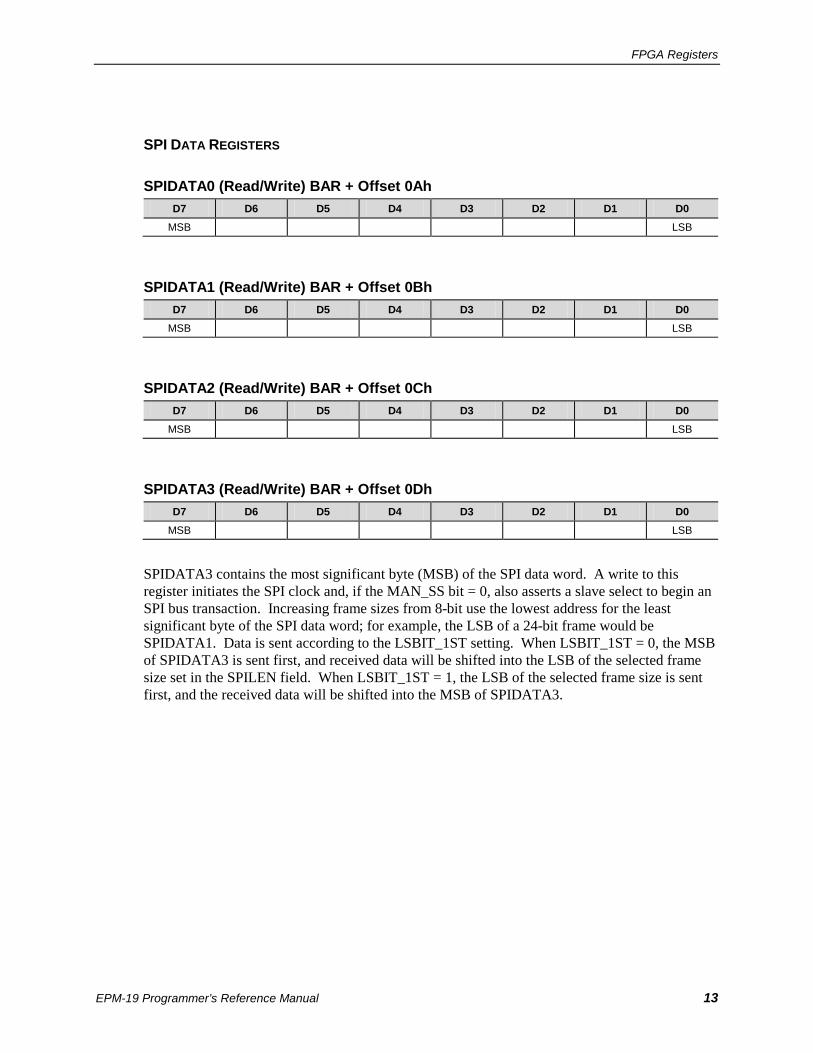
SPI DATA REGISTERS
SPIDATA0 (Read/Write) BAR + Offset 0Ah D7 D6 D5 D4 D3 D2 D1 D0
MSB LSB
SPIDATA1 (Read/Write) BAR + Offset 0Bh D7 D6 D5 D4 D3 D2 D1 D0
MSB LSB
SPIDATA2 (Read/Write) BAR + Offset 0Ch D7 D6 D5 D4 D3 D2 D1 D0
MSB LSB
SPIDATA3 (Read/Write) BAR + Offset 0Dh D7 D6 D5 D4 D3 D2 D1 D0
MSB LSB
SPIDATA3 contains the most significant byte (MSB) of the SPI data word. A write to this register initiates the SPI clock and, if the MAN_SS bit = 0, also asserts a slave select to begin an SPI bus transaction. Increasing frame sizes from 8-bit use the lowest address for the least significant byte of the SPI data word; for example, the LSB of a 24-bit frame would be SPIDATA1. Data is sent according to the LSBIT_1ST setting. When LSBIT_1ST = 0, the MSB of SPIDATA3 is sent first, and received data will be shifted into the LSB of the selected frame size set in the SPILEN field. When LSBIT_1ST = 1, the LSB of the selected frame size is sent first, and the received data will be shifted into the MSB of SPIDATA3.

FPGA Registers
EPM-19 Programmer’s Reference Manual 14
SPI DEBUG CONTROL REGISTER
Table 14: SPI – SPI Debug Control Register
Bit Identifier Access Default Description
7 Reserved RO 0 Reserved – Writes are ignored. Reads always return 0
6-4 MUXSEL(2:0) R/W 000
mSATA/PCIe Mux Selection for Minicard Slot (and 2nd SATA connector): • 000 – Select mSATA using only pin 43 (MSATA_DETECT).
This is an Intel-mode that is reliable for PCIe Minicards but not for mSATA modules that inadvertently ground this signal. This signal is purposely pulled low by the FPGA to avoid accidentally switching the SATA channel when no mSATA or PCIe Minicard is present. See the Minicard description for more info.
• 001 – Use only Pin 51 (PRES_DISABLE2#). This is the default method and is defined in the Draft mSATA spec but some Minicards use it as a second Wireless disable.
• 010 – Use either Pin 43 or Pin 51. This will work just like 001 because Pin 43 is disabled by an FPGA pull-down.
• 011 – Force PCIe mode on the Minicard • 100 – Force mSATA mode on the Minicard. • 101 – Undefined (same as 000) • 110 – Undefined (same as 000) • 111 – Undefined (same as 000) Note: When the Minicard uses PCIe, the SATA channel automatically switches to the SATA connector.
3 Reserved RO 0 Reserved. Writes are ignored; reads always return 0.
2 Reserved RO 0 Reserved. Writes are ignored; reads always return 0.
1 SPILB R/W 0
Debug/Test Only: Used to loop SPI output data back to the input (debug/test mode). 0 – Normal operation 1 – Loop SPI output data back to the SPI input data (data output still active)
0 RESERVED RO 0 Reserved. Writes are ignored; reads always return 0.

FPGA Registers
EPM-19 Programmer’s Reference Manual 15
MISCELLANEOUS FPGA REGISTERS
Table 15: MISCR1 – Misc. Control Register #1
Bit Identifier Access Default Description
7 Reserved RO 0 Reserved. Writes are ignored; reads always return 0.
6 Reserved RO 0 Reserved. Writes are ignored; reads always return 0.
5 Reserved RO 0 Reserved. Writes are ignored; reads always return 0.
4 Reserved RO 0 Reserved. Writes are ignored; reads always return 0.
3 Reserved RO 0 Reserved. Writes are ignored; reads always return 0.
2 Reserved RO 0 Reserved. Writes are ignored; reads always return 0.
1 Reserved RO 0 Reserved. Writes are ignored; reads always return 0.
0 Reserved RO 0 Reserved. Writes are ignored; reads always return 0.
Table 16: MISCSR2 – Misc. Control Register #2
Bit Identifier Access Default Description (Note)
7 NO_BATT RO N/A Indicates whether the V2 jumper is set to use a battery: 0 – Using the RTC Battery 1 – Not using the RTC Battery
6 W_DISABLE R/W 0
Controls the W_DISABLE (wireless disable) signal going to the PCIe Minicard: 0 – W_DISABLE signal is not asserted (enabled) 1 – W_DISABLE signal is asserted (disabled) There are other control sources that can be configured to control this signal and if enabled the control becomes the “OR” of all sources.
5 Reserved RO 0 Reserved. Writes are ignored; reads always return 0.
4 PBRST WO 0 Writing a 1 to this bit initiates a reset.
3 Reserved RO 0 Reserved. Writes are ignored; reads always return 0.
2 Reserved RO 0 Reserved. Writes are ignored; reads always return 0.
1 Reserved RO 0 Reserved. Writes are ignored; reads always return 0.
0 USB_OBDIS R/W 0
Disable control for the on-board USB port VBUS power switches (there are two with a common overcurrent): 0 – VBUS power switches are enabled 1 – VBUS power switched are disabled. The I2164 power switches latch-off in overcurrent and can only be re-enabled by a power-cycle or by setting this bit to a ‘1 and then a ‘0’ with at least 1 ms in between.
Note: This is a register in the always-on power well of the FPGA. It will hold its state during reboots and can only be reset by a power cycle. It is primarily used for control signals for the always-powered Ethernet controllers and the USB hubs.

FPGA Registers
EPM-19 Programmer’s Reference Manual 16
GPIO REGISTERS
AUXDIR This register controls the direction of the eight GPIO signals.
Table 17: AUXDIR – Auxiliary GPIO Direction Control Register
Bit Identifier Access Default Description
7 DIR_GPIO8 R/W 0 Sets the direction of GPIO_8 0 – Input 1 – Output
6 DIR_GPIO7 R/W 0 Sets the direction of GPIO_7 0 – Input 1 – Output
5 DIR_GPIO6 R/W 0 Sets the direction of GPIO_6 0 – Input 1 – Output
4 DIR_GPIO5 R/W 0 Sets the direction of GPIO_5 0 – Input 1 – Output
3 DIR_GPIO4 R/W 0 Sets the direction of GPIO_4 0 – Input 1 – Output
2 DIR_GPIO3 R/W 0 Sets the direction of GPIO_3 0 – Input 1 – Output
1 DIR_GPIO2 R/W 0 Sets the direction of GPIO_2 0 – Input 1 – Output
0 DIR_GPIO1 R/W 0 Sets the direction of GPIO_1 0 – Input 1 – Output

FPGA Registers
EPM-19 Programmer’s Reference Manual 17
AUXPOL This register controls the polarity of the eight GPIO signals.
Table 18: AUXPOL – Auxiliary GPIO Polarity Control Register
Bit Identifier Access Default Description
7 POL_GPIO8 R/W 0 Sets the polarity of GPIO_8 (Note) 0 – No polarity inversion 1 – Invert polarity
6 POL_GPIO7 R/W 0 Sets the polarity of GPIO_7 (Note) 0 – No polarity inversion 1 – Invert polarity
5 POL_GPIO6 R/W 0 Sets the polarity of GPIO_6 (Note) 0 – No polarity inversion 1 – Invert polarity
4 POL_GPIO5 R/W 0 Sets the polarity of GPIO_5 (Note) 0 – No polarity inversion 1 – Invert polarity
3 POL_GPIO4 R/W 0 Sets the polarity of GPIO_4 (Note) 0 – No polarity inversion 1 – Invert polarity
2 POL_GPIO3 R/W 0 Sets the polarity of GPIO_3 (Note) 0 – No polarity inversion 1 – Invert polarity
1 POL_GPIO2 R/W 0 Sets the polarity of GPIO_2 (Note) 0 – No polarity inversion 1 – Invert polarity
0 POL_GPIO1 R/W 0 Sets the polarity of GPIO_1 (Note) 0 – No polarity inversion 1 – Invert polarity
Note: This impacts the polarity as well as the interrupt status edge used.
FPGA Registers
EPM-19 Programmer’s Reference Manual 18
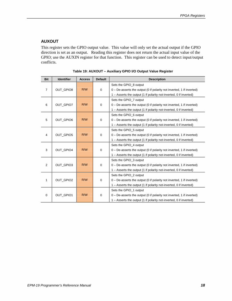
AUXOUT This register sets the GPIO output value. This value will only set the actual output if the GPIO direction is set as an output. Reading this register does not return the actual input value of the GPIO; use the AUXIN register for that function. This register can be used to detect input/output conflicts.
Table 19: AUXOUT – Auxiliary GPIO I/O Output Value Register
Bit Identifier Access Default Description
7 OUT_GPIO8 R/W 0 Sets the GPIO_8 output 0 – De-asserts the output (0 if polarity not inverted, 1 if inverted) 1 – Asserts the output (1 if polarity not-inverted, 0 if inverted)
6 OUT_GPIO7 R/W 0 Sets the GPIO_7 output 0 – De-asserts the output (0 if polarity not inverted, 1 if inverted) 1 – Asserts the output (1 if polarity not-inverted, 0 if inverted)
5 OUT_GPIO6 R/W 0 Sets the GPIO_6 output 0 – De-asserts the output (0 if polarity not inverted, 1 if inverted) 1 – Asserts the output (1 if polarity not-inverted, 0 if inverted)
4 OUT_GPIO5 R/W 0 Sets the GPIO_5 output 0 – De-asserts the output (0 if polarity not inverted, 1 if inverted) 1 – Asserts the output (1 if polarity not-inverted, 0 if inverted)
3 OUT_GPIO4 R/W 0 Sets the GPIO_4 output 0 – De-asserts the output (0 if polarity not inverted, 1 if inverted) 1 – Asserts the output (1 if polarity not-inverted, 0 if inverted)
2 OUT_GPIO3 R/W 0 Sets the GPIO_3 output 0 – De-asserts the output (0 if polarity not inverted, 1 if inverted) 1 – Asserts the output (1 if polarity not-inverted, 0 if inverted)
1 OUT_GPIO2 R/W 0 Sets the GPIO_2 output 0 – De-asserts the output (0 if polarity not inverted, 1 if inverted) 1 – Asserts the output (1 if polarity not-inverted, 0 if inverted)
0 OUT_GPIO1 R/W 0 Sets the GPIO_1 output 0 – De-asserts the output (0 if polarity not inverted, 1 if inverted) 1 – Asserts the output (1 if polarity not-inverted, 0 if inverted)

FPGA Registers
EPM-19 Programmer’s Reference Manual 19
AUXIN This register sets the GPIO input value. It reads the input value regardless of the setting on the direction (that is, it always reads the input). This reads the actual state of the GPIO pin into the FPGA.
Table 20: AUXIN – Auxiliary GPIO Input Value Register
Bit Identifier Access Default Description
7 IN_GPIO8 RO N/A
Reads the GPIO_8 input status. 0 – Input de-asserted if polarity not-inverted; asserted if polarity inverted 1 Input asserted if polarity not-inverted; de-asserted if polarity inverted
6 IN_GPIO7 RO N/A
Reads the GPIO_7 input status. 0 – Input de-asserted if polarity not-inverted; asserted if polarity inverted 1 Input asserted if polarity not-inverted; de-asserted if polarity inverted
5 IN_GPIO6 RO N/A
Reads the GPIO_6 input status. 0 – Input de-asserted if polarity not-inverted; asserted if polarity inverted 1 Input asserted if polarity not-inverted; de-asserted if polarity inverted
4 IN_GPIO5 RO N/A
Reads the GPIO_5 input status. 0 – Input de-asserted if polarity not-inverted; asserted if polarity inverted 1 Input asserted if polarity not-inverted; de-asserted if polarity inverted
3 IN_GPIO4 RO N/A
Reads the GPIO_4 input status. 0 – Input de-asserted if polarity not-inverted; asserted if polarity inverted 1 Input asserted if polarity not-inverted; de-asserted if polarity inverted
2 IN_GPIO3 RO N/A
Reads the GPIO_3 input status. 0 – Input de-asserted if polarity not-inverted; asserted if polarity inverted 1 Input asserted if polarity not-inverted; de-asserted if polarity inverted
1 IN_GPIO2 RO N/A
Reads the GPIO_2 input status. 0 – Input de-asserted if polarity not-inverted; asserted if polarity inverted 1 Input asserted if polarity not-inverted; de-asserted if polarity inverted
0 IN_GPIO1 RO N/A
Reads the GPIO_1 input status. 0 – Input de-asserted if polarity not-inverted; asserted if polarity inverted 1 Input asserted if polarity not-inverted; de-asserted if polarity inverted

FPGA Registers
EPM-19 Programmer’s Reference Manual 20
AUXIMASK This is the interrupt mask register for the GPIOs and the interrupt enables and selection.
Table 21: AUXIMASK – Auxiliary GPIO I/O Interrupt Mask and Control Register
Bit Identifier Access Default Description
7 IMASK_GPIO8 R/W 0 GPIO_8 Interrupt Mask 0 – Interrupt disabled 1 – Interrupt enabled
6 IMASK_GPIO7 R/W 0 GPIO_7 Interrupt Mask 0 – Interrupt disabled 1 – Interrupt enabled
5 IMASK_GPIO6 R/W 0 GPIO_6 Interrupt Mask 0 – Interrupt disabled 1 – Interrupt enabled
4 IMASK_GPIO5 R/W 0 GPIO_5 Interrupt Mask 0 – Interrupt disabled 1 – Interrupt enabled
3 IMASK_GPIO4 R/W 0 GPIO_4 Interrupt Mask 0 – Interrupt disabled 1 – Interrupt enabled
2 IMASK_GPIO3 R/W 0 GPIO_3 Interrupt Mask 0 – Interrupt disabled 1 – Interrupt enabled
1 IMASK_GPIO2 R/W 0 GPIO_2 Interrupt Mask 0 – Interrupt disabled 1 – Interrupt enabled
0 IMASK_GPIO1 R/W 0 GPIO_1 Interrupt Mask 0 – Interrupt disabled 1 – Interrupt enabled

FPGA Registers
EPM-19 Programmer’s Reference Manual 21
AUXISTAT This is the interrupt mask register for the GPIOs and the interrupt enables and selection.
Table 22: AUXISTAT– Auxiliary GPIO I/O Interrupt Mask and Status Register
Bit Identifier Access Default Description
7 ISTAT_GPIO8 R/WC N/A
GPIO_8 interrupt status. A read returns the interrupt status. Writing a 1 to this bit clears the interrupt status. This bit is set to a 1 on a transition from low-to-high (POL_GPIO8 = 0) or high-to-low (POL_GPIO8 = 1).
6 ISTAT_GPIO7 R/WC N/A
GPIO_7 interrupt status. A read returns the interrupt status. Writing a 1 to this bit clears the interrupt status. This bit is set to a 1 on a transition from low-to-high (POL_GPIO7 = 0) or high-to-low (POL_GPIO7 = 1).
5 ISTAT_GPIO6 R/WC N/A
GPIO_6 interrupt status. A read returns the interrupt status. Writing a 1 to this bit clears the interrupt status. This bit is set to a 1 on a transition from low-to-high (POL_GPIO6 = 0) or high-to-low (POL_GPIO6 = 1).
4 ISTAT_GPIO5 R/WC N/A
GPIO_5 interrupt status. A read returns the interrupt status. Writing a 1 to this bit clears the interrupt status. This bit is set to a 1 on a transition from low-to-high (POL_GPIO5 = 0) or high-to-low (POL_GPIO5 = 1).
3 ISTAT_GPIO4 R/WC N/A
GPIO_4 interrupt status. A read returns the interrupt status. Writing a 1 to this bit clears the interrupt status. This bit is set to a 1 on a transition from low-to-high (POL_GPIO4 = 0) or high-to-low (POL_GPIO4 = 1).
2 ISTAT_GPIO3 R/WC N/A
GPIO_3 interrupt status. A read returns the interrupt status. Writing a 1 to this bit clears the interrupt status. This bit is set to a 1 on a transition from low-to-high (POL_GPIO3 = 0) or high-to-low (POL_GPIO3 = 1).
1 ISTAT_GPIO2 R/WC N/A
GPIO_2 interrupt status. A read returns the interrupt status. Writing a 1 to this bit clears the interrupt status. This bit is set to a 1 on a transition from low-to-high (POL_GPIO2 = 0) or high-to-low (POL_GPIO2 = 1).
0 ISTAT_GPIO1 R/WC N/A
GPIO_1 interrupt status. A read returns the interrupt status. Writing a 1 to this bit clears the interrupt status. This bit is set to a 1 on a transition from low-to-high (POL_GPIO1 = 0) or high-to-low (POL_GPIO1 = 1).

FPGA Registers
EPM-19 Programmer’s Reference Manual 22
Table 23: AUXIMODE1– Auxiliary GPIO I/O Mode Register
Bit Identifier Access Default Description
7 MODE_GPIO8 R/W 0 GPIO_8 mode 0 – GPIO (I/O) 1 – Timer 0 input ICTC0 (Input)
6 MODE_GPIO7 R/W 0 GPIO_7 mode 0 – GPIO (I/O) 1 – Timer 1 input ICTC1 (Input)
5 MODE_GPIO6 R/W 0 GPIO_6 mode 0 – GPIO (I/O) 1 – Timer 0 output OCTC0 (Output)
4 MODE_GPIO5 R/W 0 GPIO_5 mode 0 – GPIO (I/O) 1 – Timer 1 output OCTC1 (Output)
3 MODE_GPIO4 R/W 0 GPIO_4 mode 0 – GPIO (I/O) 1 – Timer 0 Gate GCTC0 (Input)
2 MODE_GPIO3 R/W 0 GPIO_3 mode 0 – GPIO (I/O) 1 – Timer 1 Gate GCTC1 (Input)
1 MODE_GPIO2 R/W 0 GPIO_2 mode 0 – GPIO (I/O) 1 – Not defined
0 MODE_GPIO1 R/W 0 GPIO_1 mode 0 – GPIO (I/O) 1 – Not defined
COM PORT REGISTER
Table 24: COMMODE – COM Port Mode Control Register
Bit Identifier Access Default Description
7 Reserved RO 0 Reserved. Writes are ignored; reads always return 0.
6 Reserved RO 0 Reserved. Writes are ignored; reads always return 0.
5 Reserved RO 0 Reserved. Writes are ignored; reads always return 0.
4 Reserved RO 0 Reserved. Writes are ignored; reads always return 0.
3 COM4_TXEN R/W 0
COM4 Port RS-485 TX Enable pass-thru (must be in RS-422/485 UART mode) 0 – Drive UART “DE” input with Vortex86DX2 UART2_TXDEN 1 – Drive UART “DE” input high (always enable for RS-422)
2 COM3_TXEN R/W 0
COM3 Port RS-485 TX Enable pass-thru (must be in RS-422/485 UART mode) 0 – Drive UART “DE” input with Vortex86DX2 UART4_TXDEN 1 – Drive UART “DE” input high (always enable for RS-422)
1 Reserved RO 0 Reserved. Writes are ignored; reads always return 0.
0 Reserved RO 0 Reserved. Writes are ignored; reads always return 0.

FPGA Registers
EPM-19 Programmer’s Reference Manual 23
FPGA Interrupt Interface The FPGA signal FPGA_INT# is an active low interrupt routed to the Vortex86DX2 GPIO pin GP02. The source for this interrupt signal can be from the following FPGA functions:
Timer
SPX interface
The INTRTEST bit in the TISR may be used to test this signal connectivity since there is no SERIRQ availability for this board (because the FPGA interface is PCI based instead of LPC based).
The timer interrupts are always enabled but can be masked individually with TICR IMSK_TC(5:3). There is only one SPISTATUS register bit HW_IRQ_EN to enable/disable the SPX interrupts.

EPM-19 Programmer’s Reference Manual 24
Programming Information for Hardware Interfaces
PC/104 Expansion Bus Seven IRQs have been shown to work with the ISA bus expansion cards. As listed in Table 17, they are IRQ3, IRQ4, IRQ5, IRQ6, IRQ7, IRQ10, and IRQ11. There are conflicts with all other IRQ assignments per the Vortex86DX2 resources, and by default IRQ3, IRQ4, IRQ10, and IRQ11 are assigned to the four COM Ports. If the ISA expansion card requires more than three IRQs, you may have to disable the COM Port using the desired IRQ, taking care to ensure each of the required IRQs are reserved from PCI use in the BIOS Setup utility (PCIPnP settings). IRQ selection often requires checking to make sure the system does not have resource conflicts.
The EPM-19 has limited support of the PC/104 bus. Most PC/104 cards will work, but be sure to check the requirements of your PC/104 card against the resources listed in Table 17.
Table 25: PC/104 ISA I/O, IRQ, and Memory Resources
Available ISA I/O Addresses (Note 1)
Available ISA IRQs (Note 2)
Available ISA Memory Addresses
10 – 1F 24 – 3F 44 – 47 4C – 5F 65 67 – 6F 76 – 77 7D – 7F 90 – 91 A2 – A6 AE – B1 B4 – BF
E0 – FF 106 – 16F 178 – 1EF 1F8 – 375 377 – 3BF 3E0 – 3F5 3F7 400 – 47F 490 – 4CF 4D2 – 7FF 880 – CFBD00
IRQ3 IRQ4 IRQ5 IRQ6 IRQ7
IRQ10 IRQ11
A0000 – B7FFF C8000 – DFFFF
Notes: 1. The I/O ranges allocated to COM ports 1-4 are available to ISA only when the on-board COM ports are
disabled in the BIOS Setup utility. 2. Each of these IRQs must be reserved from the PCIPnP use in the BIOS Setup utility before they can
potentially be used on the ISA bus. Because ISA IRQ sharing is not supported, make sure that any IRQ channel used for an ISA device is not used elsewhere. For example, if ISA IRQ4 is enabled, you must use a different IRQ for COM1 to avoid resource conflicts.
4

Programming Information for Hardware Interfaces
EPM-19 Programmer’s Reference Manual 25
PCI Express Ports (PCIe) The Vortex86DX2 SoC supports two PCI Express 1.1 compliant single lane (x1) ports. Internal to the SoC is a PCI-to-PCIe bridge that provides the functionality of transactions occurring between a master on one of the internal PCI busses and a target on one of the two PCIe bus ports. Note that no SoC PCI bus is available on the SoC pins for external use. A bridge device was added to externally create a PCI interface for the board. One PCIe port is used by the PCIe-to-PCI bridge device; the other is connected to the PCIe Minicard socket.
PCIe port bifurcation is not available.
Table 26: PCIe Port Configuration
Port Source Port Speed Destination
0 Vortex86DX2 2.5 Gbits/s XIO2001 PCIe-to-PCI Bridge (to FPGA and PCI expansion slot)
1 Vortex86DX2 2.5 Gbits/s PCIe Minicard
The interrupt routing is assigned as follows in the Vortex86DX2 SoC:
PCIe Port 0: INTA, INTB, INTC, INTD
PCIe Port 1: INTB, INTC, INTD, INTA
There are certain limitations with using devices behind a PCIe-to-PCI bridge device like the XIO2001. The EPM-19 FPGA (which resides on the PCI side of the PCIe-to-PCI bridge) had to be modified to map a 1 Kbyte I/O window in order for it to function with the assigned base address per every possible board configuration. It appears that whenever the downstream devices are assigned a base address with either/both bits 9 and 8 set to 1, the downstream device is not accessible. When the base address is modified to have address bits 9 and 8 set to 0, they then become accessible.
Processor WAKE# Capabilities The PCIe-to-PCI Bridge (XIO2001) is the only device on board that drives the PCIE_WAKE# signal to the Vortex86DX2 SoC in order to “wake up” the processor. Because the Vortex86DX2 does not have a dedicated input pin for the PCIE_WAKE# function, this signal is connected to an interrupt capable GPIO pin so it is not truly compliant with the PCIe specification and may not be useful.
The PCIe Minicard has a separate “PCIE_WAKE#” signal connection (appropriately named MINI_WAKE#) to the Vortex86DX2 SoC. MINI_WAKE# is also connected to an interrupt capable GPIO pin in the same bank as the PCIE_WAKE# signal so it also is not truly compliant with the PCIe specification and may not be useful.
The following USB devices can wake up the processor using the in-band SUSPEND protocol:
USB 2.0 Ports routed to User I/O connector J9
USB Minicard via the LAN9512 hub

Programming Information for Hardware Interfaces
EPM-19 Programmer’s Reference Manual 26
GPIO Configuration Table 19 lists the EPM-19 usage of the Vortex86DX2 3.3V muxed GPIO signals. These signals are muxed between many different functional possibilities, so this list displays 8-bit blocks of GPIO port differentiation (for GPIO-P0 through GPIO-PA) with an alternating background fill pattern. GPIO-P0 contains GP00 through GP07; GPIO-P4 contains GP40 through GP47; and so on. Each signal shows whether there is an internal or external pull resistor, and when there are both the strongest pull resistor type is listed. Any GPIOs not listed are not connected.
Table 27: Vortex86DX2 GPIO Configuration
GPIO number/ Signal Use
EPM-19 signal name
Default Value
Internal or External/
Pull-Up or Down
Function
GP00/ GP interrupt input PCIE_WAKE# 1 External/
Pull-up PCIe wake interrupt
GP01/ GP interrupt input MINI_WAKE# 1 External/
Pull-up Minicard PCIe wake interrupt
GP02/ GP interrupt input FPGA_INT# 1 External/
Pull-up FPGA interrupt (for GPIO, SPX, or timers)
GP13/ GP interrupt input LVDS_PANEL_OC# 1 External/
Pull-up LVDS panel power switch over current interrupt
GP14/ GP interrupt input HUB_USB_OC# 1 External/
Pull-up Hubbed USB over current interrupt
GP15/ GP interrupt input DX2_USBOB_OC# 1 External/
Pull-up Vortex86DX2 USB (on-board) over current interrupt
GP20/ GP output DX2_RS232_SD 0 External/
Pull-down
RS-232 transceiver shutdown (COM1 and COM2) 0 = COM1 and COM2 transceivers on 1 = COM1 and COM2 transceivers shutdown
GP21/ GP output DX2_RS485_EN 1 External/
Pull-up
Multimode transceiver enable (COM3 and COM4) 0 = COM3 and COM4 transceivers off 1 = COM3 and COM4 transceivers enabled
GP22/ GP output DX2_UART2_SEL 0 External/
Pull-down
UART2 (COM3) mode selection 0 = RS-232 mode for board COM3 1 = RS-422/485 mode for board COM3
GP23/ GP output DX2_UART4_SEL 0 External/
Pull-down
UART4 (COM4) mode selection 0 = RS-232 mode for board COM4 1 = RS-422/485 mode for board COM4
GP34 Reserved 1 External/ Pull-up Reserved
GP35 Reserved 1 External/ Pull-up Reserved
GP36/ TXDEN3 output N/C – – Serial port 3 not used; SD card interface
GP37/ TXDEN4 output DX2_UART4_TXDEN X None COM4 transmit data enable (for RS-485
mode) GP40/ DCD1# input PD_UART1 0 External/
Pull-down Data Carrier Detected (tied low)
GP41/ SOUT1 output UART1_SOUT X None Serial data out / TX data (COM1, RS-232
only) GP42/ RTS1# output UART1_RTS# X None Request To Send (COM1, RS-232 only)
GP43/ RI1# input PD_UART1 0 External/
Pull-down Ring Indicator (tied low)

Programming Information for Hardware Interfaces
EPM-19 Programmer’s Reference Manual 27
GPIO number/ Signal Use
EPM-19 signal name
Default Value
Internal or External/
Pull-Up or Down
Function
GP44/ SIN1 input UART1_SIN 1 Internal/
Pull-up Serial data in / RX data (COM1, RS-232 only)
GP45/ DTR1# output N/C - - Not used
GP46/ DSR1# input PD_UART1_ 0 Internal/
Pull-down Data Set Ready (tied low)
GP47/ CTS1# input UART1_CTS# 1 Internal/
Pull-up Clear To Send (COM1, RS-232 only)
GP50/ DCD2# input PD_UART2# 0 External/
Pull-down Data Carrier Detected (tied low)
GP51/ SOUT2 output UART2_TXD X None TX data (COM2, RS-232/RS-422/RS-485)
GP52/ RTS2# output UART2_RTS# X None Request To Send (COM2, RS-232/RS-
422/RS-485) GP53/ RI2# input PD_UART2# 0 External/
Pull-down Ring Indicator (tied low)
GP54/ SIN2 input UART2_RXD 1 Internal/
Pull-up RX data (COM2, RS-232/RS-422/RS-485)
GP55/ DTR2# output N/C – – Not used
GP56/ DSR2# input PD_UART2# 0 External/
Pull-down Data Set Ready (tied low)
GP57/ CTS2# input UART2_CTS# 1 Internal/
Pull-up Clear To Send (COM2, RS-232/RS-422/RS-485)
GP60/ SD0_D2 bi-dir DX2_SD_DATA2_R 1 External/
Pull-up microSD card data bit 2
GP61/ SD0_D3 bi-dir DX2_SD_DATA3_R 1 External/
Pull-up microSD card data bit 3
GP62/ SD0_CMD bi-dir DX2_SD_CMD_R 1 External/
Pull-up microSD card command
GP63/ SD0_CLK output CLK_DX2_SD_R 0 Internal/
Pull-down microSD card clock
GP64/ SD0_D0 bi-dir DX2_SD_DATA0_R 1 External/
Pull-up microSD card data bit 0
GP65/ SD0_D1 bi-dir DX2_SD_DATA1_R 1 External/
Pull-up microSD card data bit 1
GP66/ SD0_CD input DX2_SD_CD# 1 External/
Pull-up microSD card detect (low when card installed)
GP67/ SD0_WP input DX2_SD_WP 0 External/
Pull-down microSD card write protect
GP70/ DCD4# input PD_UART4# 0 External/
Pull-down Data Carrier Detected (tied low)
GP71/ SOUT4 output UART4_TXD X None TX data (COM4, RS-232/RS-422/RS-485)
GP72/ RTS4# output UART4_RTS# X None Request To Send (COM4, RS-232/RS-
422/RS-485) GP73/ RI2# input PD_UART4# 0 External/
Pull-down Ring indicator (tied low)
GP74/ SIN2 input UART4_RXD 1 Internal/
Pull-up RX data (COM4, RS-232/RS-422/RS-485)
GP75/ DTR2# output N/C – – Not used
GP76/ DSR2# input PD_UART4# 0 External/
Pull-down Data Set Ready (tied low)
GP77/ CTS2# input UART4_CTS# 1 Internal/
Pull-up Clear To Send (COM4, RS-232/RS-422/RS-485)
GP80/ DCD9# input PD_UART9 0 External/
Pull-down Data Carrier Detected (tied low)
GP81/ SOUT9 output UART9_SOUT X None Serial data out / TX data (COM2, RS-232
only) GP82/ RTS9# output UART9_RTS# X None Request To Send (COM2, RS-232 only)

Programming Information for Hardware Interfaces
EPM-19 Programmer’s Reference Manual 28
GPIO number/ Signal Use
EPM-19 signal name
Default Value
Internal or External/
Pull-Up or Down
Function
GP83/ RI9# input PD_UART9_ 0 External/
Pull-down Ring Indicator (tied low)
GP84/ SIN9 input UART9_SIN 1 Internal/
Pull-up Serial data in / RX data (COM2, RS-232 only)
GP85/ DTR9# output N/C - - Not used
GP86/ DSR9# input PD_UART9 0 External/
Pull-down Data Set Ready (tied low)
GP87/ CTS9# input UART9_CTS# 1 Internal/
Pull-up Clear To Send (COM2, RS-232 only)
GP97/ WDTOUT1 output DX2_WDTOUT1 X None Watchdog 1 timeout signal
GPA6/ TXDEN2 output DX2_UART2_TXDEN X None COM3 Transmit Data Enable (for RS-485
mode) GPA7/ TXDEN1 output N/C – – Not used, COM1 is RS-232 only
Industrial I/O Functions and SPI Interface The EPM-19 employs a set of I/O registers for controlling external serial peripheral interface (SPI) devices. These functions share control and data registers located at I/O addresses whose range depends on programmed FPGA PCI BAR added to offsets 0x00-0xFF. See the section titled Accessing the FPGA, beginning on page 4 for more information.
The SPI bus specifies four logic signals:
SCLK – Serial clock (output from master)
MOSI – Master output, slave input (output from master)
MISO – Master input, slave output (output from slave)
SS – Slave select (output from master)
The EPM-19 SPI implementation adds additional features, such as hardware interrupt input to the master. The master initiates all SPI transactions. A slave device responds when its slave select is asserted and it receives clock pulses from the master.
Slave selects are controlled in one of two modes: manual or automatic. In automatic mode, the slave select is asserted by the SPI controller when the most significant data byte is written. This initiates a transaction to the specified slave device. In manual mode, the slave select is controlled by the user and any number of data frames can be sent. The user must command the slave select high to complete the transaction.
The SPI clock rate can be software configured to operate at speeds between 1 MHz and 8 MHz. All four common SPI modes are supported through the use of clock polarity and clock phase controls.
To initiate an SPI transaction, configure SPI registers SPICONTROL and SPISTATUS as shown in Table 12 and Table 13 for the desired I/O device. For additional information on communicating with specific SPI devices, refer to their respective manufacturer’s datasheets.

Programming Information for Hardware Interfaces
EPM-19 Programmer’s Reference Manual 29
Serial Ports The EPM-19 includes four on-board 16550-based serial channels located at standard PC I/O addresses. Each COM port can be independently enabled or disabled in the BIOS Setup utility.
All four COM ports by default are set to RS-232 mode
COM1 and COM2 are RS-232 (up to 115.2K baud) serial ports. There are no configuration jumpers for COM1 and COM2 because they only operate in RS-232 mode. IRQ lines are chosen in the BIOS Setup utility.
COM3 and COM4 can be operated in RS-232 or RS-422/485 mode. IRQ lines are chosen in the BIOS Setup utility, but software configuration is required to set the COM3 and COM4 transceivers to RS-422/485 mode.
Additional non-standard baud rates are also available through the BIOS Setup utility.
COM3/COM4 HARDWARE CONFIGURATION Refer to the EPM-19 Hardware Reference Manual for information on the settings for jumper block V1 required for using COM3 and COM4 in RS-422/485 modes.
COM3/COM4 SOFTWARE CONFIGURATION By default, COM3 and COM4 are configured for RS-232 operation. Two registers in the Vortex86DX2 (0x9A and 0x7A) need to be programmed for COM3 and/or COM4 to operate in RS-422 or RS-485 mode. Table 23 and Table 24 provide bit-level descriptions of these registers. Note that there is also a register setting in the FPGA that should be configured when using RS-422 mode (the default assignment supports RS-232 and RS-485 operating modes). Refer to the section titled COM Port Register on page 22.
To configure COM3 and COM4 for RS-422/485 Mode
1. Write 0xFF to I/O register 0x9A (sets GPIO-P2[7:0] to outputs)
2. Write 0x0E to I/O register 0x7A (disables RS-232 mode and enables transceivers)
To reconfigure COM3 and COM4 for RS-232 Mode
1. Write 0xFF to I/O register 0x9A (sets GPIO-P2[7:0] to outputs)
2. Write 0x02 to I/O register 0x7A (enables RS-232 mode and enables transceivers)

Programming Information for Hardware Interfaces
EPM-19 Programmer’s Reference Manual 30
Table 28: GPIO Port 2 Direction Register – 0x9A
Bit Description
7 0 = Sets pin 7 to input mode 1 = Sets pin 7 to output mode
6 0 = Sets pin 6 to input mode 1 = Sets pin 6 to output mode
5 0 = Sets pin 5 to input mode 1 = Sets pin 5 to output mode
4 0 = Sets pin 4 to input mode 1 = Sets pin 4 to output mode
3 0 = Sets pin 3 to input mode 1 = Sets pin 3 to output mode
2 0 = Sets pin 2 to input mode 1 = Sets pin 2 to output mode
1 0 = Sets pin 1 to input mode 1 = Sets pin 1 to output mode
0 0 = Sets pin 0 to input mode 1 = Sets pin 0 to output mode
Table 29: GPIO Port 2 Data Register – 0x7A
Bit Description
7-4 X – Don’t care
3 0 = Sets COM4 to RS-232 mode 1 = Sets COM4 to RS-422/485 mode
2 0 = Sets COM3 to RS-232 mode 1 = Sets COM3 to RS-422/485 mode
1 0 = Disables multi-protocol serial transceivers (COM3 and COM4 only) 1 = Enables multi-protocol serial transceivers (COM3 and COM4 only)
0 0 = Enables RS-232 transceivers (COM1 and COM2 only) 1 = Disables RS-232 transceivers (COM1 and COM2 only)
SERIAL PORT ASSIGNMENT The EPM-19 only supports the use of the Vortex86DX2 Serial Ports 1, 2, 4, and 9, so all other serial ports are disabled and not available in the BIOS Setup utility. Table 25 lists the recommended settings (tested with Windows 7) for the Vortex86DX2 serial ports.
Table 30: Recommended Serial Port Settings for Vortex86DX2 BIOS
Vortex86DX2 Serial Port # I/O Address IRQ EPM-19 COM # (Note) 1 3F8h 4 COM1 2 3E8h 3 COM3 4 2E8h 11 COM4 9 2F8h 10 COM2
Note: COM ports are numbered to match EPM-19 I/O connector COM numbering.

Programming Information for Hardware Interfaces
EPM-19 Programmer’s Reference Manual 31
COM PORTS (FIFO UARTS) The EPM-19 supports two RS232 8-wire COM ports and two multiprotocol (RS-232/422/485) 4-wire COM ports. The COM ports are 16C550 compatible with default internal pull-ups, a programmable baud rate generator with the data rate from 2400 bps to 115,200 bps (standard baud rates, 115,200 bps is default), and also high-speed settings from 31,200 bps to 748,800 bps (only useful for COM3 and COM4 in RS-422 or RS-485 modes). The multiprotocol ports support RS-422, and also RS-485 with auto-direction control when the jumper settings for V1 are configured correctly.
Port 80h output data can be sent to COM1 via the BIOS Setup utility by enabling “P.O.S.T. Forward to SB COM1” under the Chipset/Southbridge settings.
The Vortex86DX2 has many functions that are multiplexed with others. Because of this and the fact that only some of the UARTs supported multiprotocol usage, non-standard UART numbers were used to create COM ports for the EPM-19. Here is a list of the default settings for the UARTs:
Vortex86DX2 UART 1 (EPM-19 COM1) defaults to 3F8h – 3FFh at IRQ4
Vortex86DX2 UART 9 (EPM-19 COM2) defaults to 2F8h – 2FFh at IRQ10
Vortex86DX2 UART 2 (EPM-19 COM3) defaults to 3E8h – 3EFh at IRQ3
Vortex86DX2 UART 4 (EPM-19 COM4) defaults to 2E8h – 2EFh at IRQ11
By default, all COM ports…
o are enabled in the BIOS
o are set to 115,200 bps (baud rate)
o are set to RS-232 mode.
o use a 32-byte FIFO
During Verification testing, the COM ports displayed data compare errors intermittently while running Windows 7 Passmark BurnIn Test with a moderate to heavy loaded system. Since IRQ priorities and small data FIFOs are involved here, users should expect some lost COM port data (especially on the lower priority IRQ COM ports) when using multiple COM ports with a heavily-loaded system.
COM PORT BAUD RATE SUPPORT The Vortex86DX2 SoC supports many different baud rates. Standard baud rates using a base clock rate of 1.8432 MHz run up to 230.4 kbps. COM1, COM2, COM3, and COM4 have been tested using standard baud rates up to 115.2 kbps with RS-232 signaling. COM3 and COM4 were then tested further using high-speed baud rates (using non-standard base clock rate of 24 MHz), allowing operation up to 1 Mbps per the multiprotocol transceiver set to RS-422 mode with the endpoint termination enabled on the ports.
Table 26 and Table 27 are provided as a reference should you need to access the control registers independent of any standard serial port application.
First, determine your PCI register access address using the PCI Bus 0x00 Device 0x07 Function 0x00 <insert hex value of chosen offset address per Table 26 in the PCI Address column>:
Programming Information for Hardware Interfaces
EPM-19 Programmer’s Reference Manual 32
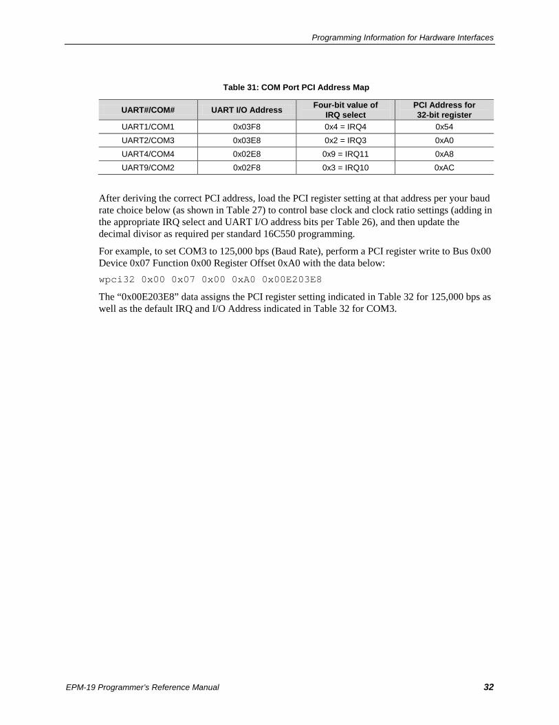
Table 31: COM Port PCI Address Map
UART#/COM# UART I/O Address Four-bit value of IRQ select
PCI Address for 32-bit register
UART1/COM1 0x03F8 0x4 = IRQ4 0x54 UART2/COM3 0x03E8 0x2 = IRQ3 0xA0 UART4/COM4 0x02E8 0x9 = IRQ11 0xA8 UART9/COM2 0x02F8 0x3 = IRQ10 0xAC
After deriving the correct PCI address, load the PCI register setting at that address per your baud rate choice below (as shown in Table 27) to control base clock and clock ratio settings (adding in the appropriate IRQ select and UART I/O address bits per Table 26), and then update the decimal divisor as required per standard 16C550 programming.
For example, to set COM3 to 125,000 bps (Baud Rate), perform a PCI register write to Bus 0x00 Device 0x07 Function 0x00 Register Offset 0xA0 with the data below: wpci32 0x00 0x07 0x00 0xA0 0x00E203E8
The “0x00E203E8” data assigns the PCI register setting indicated in Table 32 for 125,000 bps as well as the default IRQ and I/O Address indicated in Table 32 for COM3.

Programming Information for Hardware Interfaces
EPM-19 Programmer’s Reference Manual 33
Table 32: Baud Rates, Divisors, and Base Clock and Ratio Selection for UARTs
Baud rate (bps)
"Crystal" base clock Clock ratio Decimal
divisor Standard or high-speed
PCI register setting
(32-bits) [Note]
1200 1.8432 MHz 1/16 96 Standard 00Axyyyy 2400 1.8432 MHz 1/16 48 Standard 00Axyyyy 4800 1.8432 MHz 1/16 24 Standard 00Axyyyy 9600 1.8432 MHz 1/16 12 Standard 00Axyyyy
14,400 1.8432 MHz 1/16 8 Standard 00Axyyyy 19,200 1.8432 MHz 1/16 6 Standard 00Axyyyy 28,800 1.8432 MHz 1/16 4 Standard 00Axyyyy 38,400 1.8432 MHz 1/16 3 Standard 00Axyyyy 57,600 1.8432 MHz 1/16 2 Standard 00Axyyyy
115,200 1.8432 MHz 1/16 1 Standard 00Axyyyy 230,400 1.8432 MHz 1/8 1 Standard 00Bxyyyy 15,625 24 MHz 1/16 96 High-speed 00Exyyyy 31,250 24 MHz 1/16 48 High-speed 00Exyyyy 62,500 24 MHz 1/16 24 High-speed 00Exyyyy
125,000 24 MHz 1/16 12 High-speed 00Exyyyy 250,000 24 MHz 1/16 6 High-speed 00Exyyyy 500,000 24 MHz 1/16 3 High-speed 00Exyyyy 750,000 24 MHz 1/16 2 High-speed 00Exyyyy 214,286 24 MHz 1/8 14 High-speed 00Fxyyyy 230,769 24 MHz 1/8 13 High-speed 00Fxyyyy 250,000 24 MHz 1/8 12 High-speed 00Fxyyyy 428,571 24 MHz 1/8 7 High-speed 00Fxyyyy 500,000 24 MHz 1/8 6 High-speed 00Fxyyyy 750,000 24 MHz 1/8 4 High-speed 00Fxyyyy
1,000,000 24 MHz 1/8 3 High-speed 00Fxyyyy Note:
• x = IRQ Select • yyyy = Address
Programmable LED
User I/O connector J9 includes an output signal for attaching a software controlled LED. Connect the cathode of the LED to J9, pin 16; connect the anode to +5V. An on-board resistor limits the current to 15 mA when the circuit is turned on. A programmable LED is provided on the CBR-4005B paddleboard. Refer to the EPM-19 Hardware Reference Manual for the location of the Programmable LED on the CBR-4005B paddleboard.
To switch the PLED on and off, refer to the section titled Accessing the FPGA, beginning on page 4.

EPM-19 Programmer’s Reference Manual 34
Appendix A – References
Overview of Vortex86DX2 http://www.vortex86.com/?p=16
Data sheet for ILAN9512 – USB 2.0 Hub and 10/100 Ethernet Controller
http://ww1.microchip.com/downloads/en/DeviceDoc/9512.pdf
Data sheet for Microchip MCP23S17 – 16-Bit I/O expander with serial interface
http://www.versalogic.com/support/Downloads/PDF/MCP23S17%20IO%20expander.pdf
*** End of document ***
A