project esa qca0416s c heavy ion effects on bias
TRANSCRIPT
Reg. Office:
Saab Ericsson Space AB Telephone: Linköping Office: Telephone:
S-405 15 Göteborg +46 31 735 00 00 Saab Ericsson Space AB +46 13 18 64 00
Sweden Telefax: S-581 88 Linköping Telefax:
Reg. No: 556134-2204 +46 31 735 40 00 Sweden +46 13 13 16 28
Document No
D-P-REP-01404-SE
Date Issue Page
2005-05-12 1 1/21
PROJECT
ESA_QCA0416S_C
TITLE
Name Function Date Signature
Prepared : S. Larsson
S. Mattsson
Approved : Reno Harboe Sorensen
Distribution
Complete :
Summary :
Heavy Ion Effects on Bias Conditions in AC/HC logic IC’s
EUROPEAN SPACE AGENCY
CONTRACT REPORT
The work described in this report was done under ESA contract. Responsibility for the contents resides in the
author or organisation that prepared it.

Page : 2 Document No D-P-REP-01388-SE Date : 2005-05-12 Issue : 1
SUMMARY
This report presents the results of a heavy ion Single Event Effects (SEEs) tests of
54AC/ 54HC logics as a function of three bias voltage conditions (2.5V, 3.3V and 5V).
Tested devices were:
54HC08, 54HC157, 54HC273, 54HC4040, 54HC4053 from ST Microelectronics
54AC08, 54AC153, 54AC257, 54AC244, 54AC273 from ST Microelectronics
54AC08, 54AC153, 54AC257, 54AC244, 54AC273 from National Semiconductor
The selected logic gate devices 54XX08, 54XX157, 54XX244 and 54XX257 are found
to be insensitive to heavy ions up to an LET of 110 MeV/mg/cm2 (see Table 4.1 for
details).
The analog multiplexer/demultiplexer 54HC4053 show the same SET sensitivity for all
bias voltage levels.
The digital 54AC/HC273 and 54HC4040 logics indicate higher susceptibility to
SEU/SET when operated at lower voltages. The relationship observed between
threshold-LET and bias voltage level varied between the digital device types. The
largest effect of decreasing voltage was observed between 5V and 3.3V.
DOCUMENT CHANGE RECORD
Changes between issues are marked with a left-bar.
Issue Date Paragraphs affected Change information
1 2005-05-12 All New document
Class : Host System :
Contract No : Host File : ...\AC-HC_reviewed-2_RHS.25534DEFANGED-doc
Page : 3 Document No D-P-REP-01388-SE Date : 2005-05-12 Issue : 1
TABLE OF CONTENTS PAGE
1. ABSTRACT ................................................................................................ 4
2. INTRODUCTION ....................................................................................... 4
2.1 References ................................................................................................. 4
3. TESTING TECHNIQUES and TEST SAMPLES ...................................... 5
3.1 Heavy Ion Test Facility ............................................................................. 5
3.2 54AC08 / 54HC08 – Quad 2-Input and Gate............................................ 6
3.3 54AC157 / 54HC157 – Quad 2-Channel Multiplexer .............................. 7
3.4 54AC244 Octal Buffers with Tri-State Outputs........................................ 8
3.5 54AC257 Quad 2-to-1 Line Selector/Multiplexer .................................... 9
3.6 54AC273 / HC273 – Octal D Type Flip-Flop with Clear ....................... 10
3.7 54HC4040 – 12 Stage Binary Ripple Counter ........................................ 11
3.8 54HC4053 – Analog Mux / Demux, Triple 2 Channel ........................... 12
4. RESULTS.................................................................................................. 13
4.1 General .................................................................................................... 13
4.2 Logic Circuits .......................................................................................... 13
4.3 Analog Circuits ....................................................................................... 16
5. CONCLUSION ......................................................................................... 17
6. APPENDIX ............................................................................................... 18

Page : 4 Document No D-P-REP-01388-SE Date : 2005-05-12 Issue : 1
1. ABSTRACT
This report presents the results of a heavy ion evaluation of five types of AC/HC logic
IC’s from National Semiconductor and ST Microelectronics. Single Event Effects
(SEEs) have been studied as a function of bias conditions. The studies have been
undertaken during the year 2004 on an ESA contract No. 11409-COO-8/I. All tests were
carried at the CYClotron of LOuvain la NEuve (CYCLONE) in Belgium.
2. INTRODUCTION
The growing trend towards lower bias voltage has begun to influence space electronics
systems. It is therefore important to assess SEU and SEL vulnerability of CMOS
devices at reduced bias voltage levels.
The purpose of these tests was to determine the SEE characteristics of AC/HC logics as
a function of the bias voltage conditions. Earlier [1] five types of 54HC logic family
from ST Microelectronics (54HC08, 54HC157, 54HC273, 54HC4040, 54HC4053) have
been tested at 5Volt bias condition. In the present tests the same five types of 54HC
have been selected together with five 54AC types from two manufacturers.
The aim was to select the same types of 54AC logics from ST Microelectronics and
National Semiconductor as the selected 54HC types. However, all five types do not
exist in 54AC from both manufacturer and therefore, five part types were selected
where the AC types from both manufacturer could be compared (54AC08, 54AC153,
54AC257, 54AC244, 54AC273). All types have been tested at 2.5V, 3.3V and 5V bias
condition.
2.1 References
[1] H. Constans, C. Tizon, F.X.Guerre, R. Harboe Sorensen,
Heavy ion testing of 54HC from SGS Thomson, Hirex report HRX/97.2770
[2] F. Sturesson, m. Wiktorson, S. Mattsson, S. Larsson, R. Harboe Sorensen
Saab Ericsson Space Test report D-PL-REP-5162-SE /ESA-QCA0202S_C

Page : 5 Document No D-P-REP-01388-SE Date : 2005-05-12 Issue : 1
3. TESTING TECHNIQUES and TEST SAMPLES
Test boards according to drawings for each part type were developed and controlled by
a PC computer via GPIB interface. When applicable, two oscilloscopes have been used
(Tektronix TDS3054, 500 MHz, 5GS/s) to count the number of events and to store the
pulse profile of the events. The test software was developed by use of “Labview
software” for the GPIB communication between the computer and the oscilloscopes /
test boards. All results were stored as common ”Excel-files”.
All devices were tested under three bias condition, +5 VDC, +3.3VDC and +2.5VDC.
Schematic drawings of the test set-ups are given below.
3.1 Heavy Ion Test Facility
Heavy ion tests were performed at the CYClotron of Louvain la Neuve (CYCLONE) in
Belgium. The experiments have been performed in 2004 during three different test
campaigns. In each campaign the actual ion cocktail in use have been utilized.
The ions used from the standard (M/Q=5)* and the high energy (M/Q=3.33) cocktail are
given in Table 3.9.1 below.
TABLE 3.9.1 HEAVY IONS USED AT LOUVAIN LA NEUVE IN BELGIUM
Element Energy
MeV Range
µm
LET value
[ MeV/mg/cm2 ]
40Ar 372 119 10.1
40Ar* 150 42 14.1
58Ni 500 85 21.9
78Kr 756 92 32.4
78Kr* 316 43 34.0
132Xe* 459 43 55.9
Page : 6 Document No D-P-REP-01388-SE Date : 2005-05-12 Issue : 1
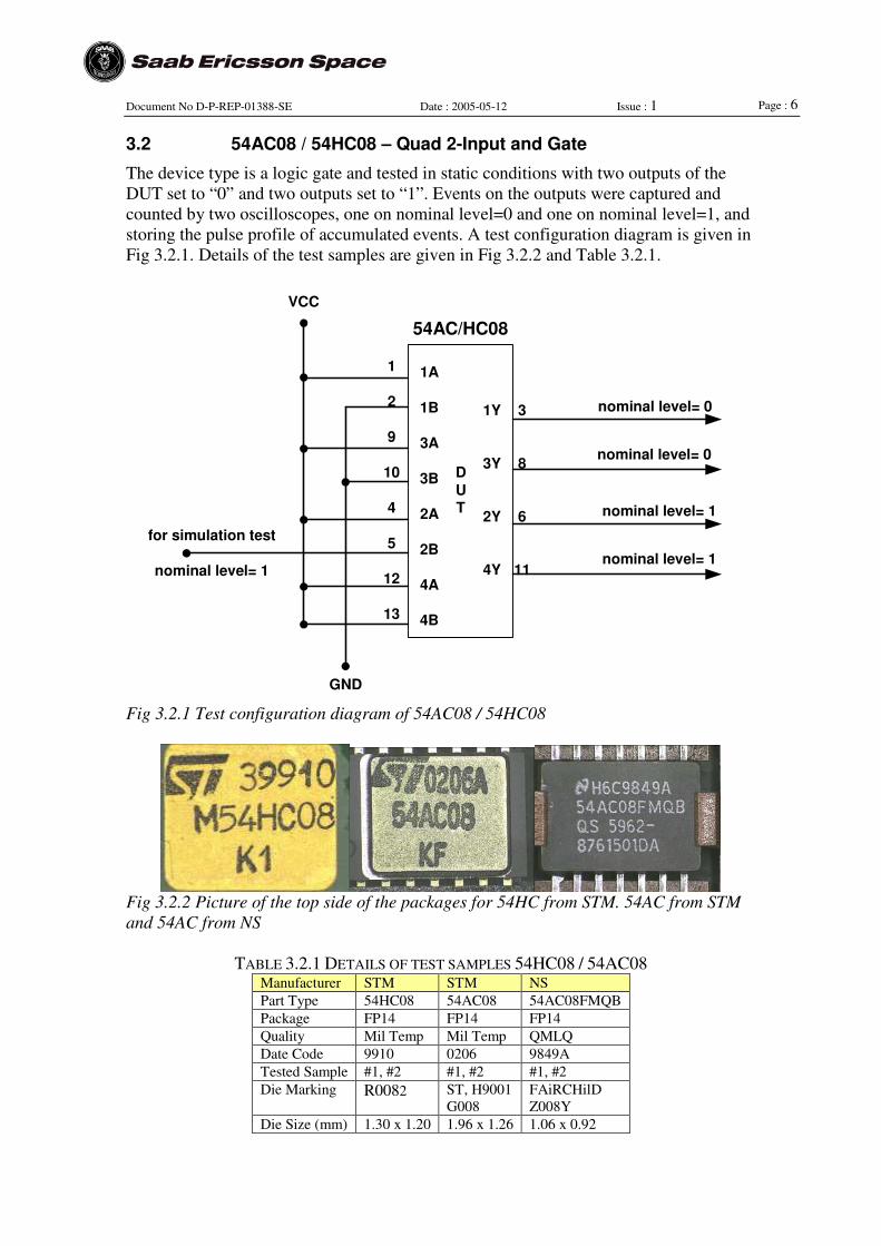
3.2 54AC08 / 54HC08 – Quad 2-Input and Gate
The device type is a logic gate and tested in static conditions with two outputs of the
DUT set to “0” and two outputs set to “1”. Events on the outputs were captured and
counted by two oscilloscopes, one on nominal level=0 and one on nominal level=1, and
storing the pulse profile of accumulated events. A test configuration diagram is given in
Fig 3.2.1. Details of the test samples are given in Fig 3.2.2 and Table 3.2.1.
1
2
9
10
4
5
12
13
GND
VCC
for simulation test
nominal level= 1
1A
1B
3A
3B
2A
2B
4A
4B
1Y
3Y
2Y
4Y
3
8
6
11
nominal level= 0
nominal level= 0
nominal level= 1
nominal level= 1
54AC/HC08
D
UT
Fig 3.2.1 Test configuration diagram of 54AC08 / 54HC08
Fig 3.2.2 Picture of the top side of the packages for 54HC from STM. 54AC from STM
and 54AC from NS
TABLE 3.2.1 DETAILS OF TEST SAMPLES 54HC08 / 54AC08 Manufacturer STM STM NS
Part Type 54HC08 54AC08 54AC08FMQB
Package FP14 FP14 FP14
Quality Mil Temp Mil Temp QMLQ
Date Code 9910 0206 9849A
Tested Sample #1, #2 #1, #2 #1, #2
Die Marking R0082 ST, H9001
G008
FAiRCHilD
Z008Y
Die Size (mm) 1.30 x 1.20 1.96 x 1.26 1.06 x 0.92

Page : 7 Document No D-P-REP-01388-SE Date : 2005-05-12 Issue : 1
3.3 54AC157 / 54HC157 – Quad 2-Channel Multiplexer
The device type is logic circuit data selector and tested in static conditions in the same
way as 54AC08 / 54HC08 with two oscilloscopes, one on nominal level=0 triggering on
positive slope and one on nominal level=1 triggering on negative slope. A test
configuration diagram is given in Fig 3.3.1. Details of the test samples are given in Fig
3.3.2 and Table 3.3.1
2
5
10
13
3
6
11
14
1
15
1A
1B
2A
2B
3A
3B
4A
4B
A/B
__
E
1Y
2Y
3Y
4Y
4
7
9
12
nominal level = 0
nominal level= 0
nominal level= 1
nominal level= 1
54AC/HC157
D
U
T
VCC
GND
for simulationtest
nominal level =1
Fig 3.3.1 Test configuration diagram of 54AC157 / 54HC157
Fig 3.3.1 Picture of the top side of the packages for 54HC from STM. 54AC from STM
and 54AC from NS
TABLE 3.3.1 DETAILS OF TEST SAMPLES 54HC157 / 54AC157 Manufacturer STM STM NS
Part Type 54HC157 54AC157 54AC157
Package FP16 FP16 FP16
Quality Mil Temp Mil Temp QMLQ
Date Code 9915 0315A 9718A
Tested Sample #1, #2 #1, #2 #1, #2
Die Marking R157 ST
G157
FAiRCHilD
Z157Y
Die Size (mm) 1.90 x 1.36 1.78 x 1.22 1.16 x 1.16
Page : 8 Document No D-P-REP-01388-SE Date : 2005-05-12 Issue : 1
3.4 54AC244 Octal Buffers with Tri-State Outputs
This device type is tested in static conditions for all three states.
Two modes when the Output Enable is set to truth, 1Y0 & 1Y1 are forced to high and
1Y2 and 1Y3 are forced to low. Two modes when the Output Enable is set to false, i.e.
when the output is in the high impedance mode; 2Y0 and 2Y1 are galvanic connected to
ground via resistors and will test 0 to 1 false; 2Y1 & 2Y2 will test 1 to 0 false.
Events from the NAND / OR were captured and counted by two oscilloscopes, which
also stored the pulse profile of accumulated events. A test configuration diagram is
given in Fig 3.4.1. Details of the test samples are given in Fig 3.4.2 and Table 3.4.1.
__1OE
1A0
1A1
1A2
1A3
2A0
2A1
2A2
2A3
__
2OE
1Y0
1Y1
1Y2
1Y3
2Y0
2Y1
2Y2
2Y3
GND
1
2
4
6
8
11
13
15
17
VCC
19
18
16
14
12
9
7
5
3
N
A
N
D
O
R
OR
N
AN
D
54AC244
DU
T
Nominal levelsout
are low (=0)
GNDVCC
1 to 0 fault
0 to 1 fault
0 to 1 fault
Tristate
1 to 0 fault
Tristate
All resistances =1 Mohm
Fig 3.4.1 Test configuration diagram of 54AC244
Fig 3.4.2 Picture of the top side of the packages for 54AC from STM and 54AC from NS
TABLE 3.4.1 DETAILS OF 54AC244 Manufacturer STM NS
Part Type 54AC244 54AC244
Package FP20 FP20
Quality Mil Temp QMLQ
Date Code 0101A 0323A
Tested Sample #1, #2 #1, #2
Die Marking ST, N2403
N244
NSFM, Z244W
J240W
Die Size (mm) 1.86 x 1.24 1.48 x 1.36

Page : 9 Document No D-P-REP-01388-SE Date : 2005-05-12 Issue : 1
3.5 54AC257 Quad 2-to-1 Line Selector/Multiplexer
Single Event Transients (SET) pulses were measured using a feeding-and-counting
technique[2]. The DUT board was connected to a LVDS driver on the input and a
LVDS receiver on the output. Dynamic tests were performed by feeding the driver with
accurate known frequency (2.5 MHz) and measuring the response at the receiver side
after the frequency train has passed the DUT during irradiation. As the feeding-
counting system a Pulse-/Pattern generator (HP81130A 400/660 MHz) were used
together with a High Resolution programmable Timer/Counter (Fluke PM6680B). Any
difference between fed and measured frequency will be reported as an SET.
A test configuration diagram is given in Fig 3.5.1. Details of the test samples are given
in Fig 3.5.2 and Table 3.5.1.
G
4A
4B
4Y
3A
3B
3Y
A/B
1A
1B
1Y
2A
2B
2Y
CL IN
CL OUT
54AC257
D
U
T
L R
V E
D C
S .
GEN.
L D
V R
D I
S V
COUNTER
VCC
Fig 3.5.1 Test configuration diagram of 54AC257
Fig 3.5.2 Picture of the top side of the packages for 54AC257 from STM and 54AC257
from NS
TABLE 3.5.1 DETAILS OF 54AC257 Manufacturer STM NS
Part Type 54AC257 54AC257
Package FP16 FP16
Quality MIL Temp QMLQ
Date Code 9844 9951A
Tested Sample #1, #2 #1, #2
Die Marking ST, N257
N257l
FAiRCHilD
J157X, Z257X
Die Size (mm) 1.70 x 1.26 1.22 x 1.22

Page : 10 Document No D-P-REP-01388-SE Date : 2005-05-12 Issue : 1
3.6 54AC273 / HC273 – Octal D Type Flip-Flop with Clear
The device is tested continuously during irradiation according to the set-up shown in
Fig 3.6.1. Computer generated data patterns are fed thru the device at a frequency of 25
kHz. Details of the test samples are given in Fig 3.6.2 and Table 3.6.1
2
74HC4050
54AC/HC27374HC244
pattern
generator
00/FF
by
computer
read and
compare
by
computer
3
4
7
8
13
14
17
18
D0
D1
D2
D3
D4
D5
D6
D7
CP__
MR
VCC
Q0
Q1
Q2
Q3
Q4
Q5
Q6
Q7
2
5
6
9
12
15
16
19
DU
T
Fig 3.6.1 Test configuration diagram of 54AC273 / 54HC273. Logics at input and
output are used for voltage adoption to the various test voltages of the DUT.
Fig 3.6.2 Picture of the top side of the packages for 54HC273 from STM. 54AC273
from STM and 54AC273 from NS
TABLE 3.6.1 DETAILS OF TEST SAMPLES 54HC273 / 54AC273 Manufacturer STM STM NS
Part Type 54HC273 54AC273 54AC273
Package FP20 FP20 FP20
Quality Mil Temp Mil Temp QMLQ
Date Code 9527 0316A 9548A
Tested Sample #1, #2 #1, #2 #1, #2
Die Marking R273 2 ST, N273 FAiRCHilD
Z273Z
Die Size (mm) 2.04 x 1.80 2.00 x 1.12 1.66 x 1.46

Page : 11 Document No D-P-REP-01388-SE Date : 2005-05-12 Issue : 1
3.7 54HC4040 – 12 Stage Binary Ripple Counter
The device has been tested in a golden chip configuration. During irradiation the 12-bits
output word of the DUT and the golden chip was compared synchronously at each clock
period at a rate of 2.5 MHz. Errors were stored on PC. A test configuration diagram is
given in Fig 3.7.1. Details of the test samples are given in Fig 3.7.2 and Table 3.7.1
CL IN
FALSE
OUT
D
UT
G
O
L
DE
N
D
E
V
54HC4040
74HC574
74HC688
Fig 3.7.1 Test configuration diagram of 54HC4040
Fig 3.7.2 Picture of the top side of the package for 54HC4040 from STM
TABLE 3.7.1 DETAILS OF 54HC4040 Manufacturer STM
Part Type 54HC4040
Package FP16
Quality Mil Temp
Date Code 0136
Tested Sample 61 & 62
Die Marking Z440
Die Size (mm) 2.44 x 1.74
Page : 12 Document No D-P-REP-01388-SE Date : 2005-05-12 Issue : 1
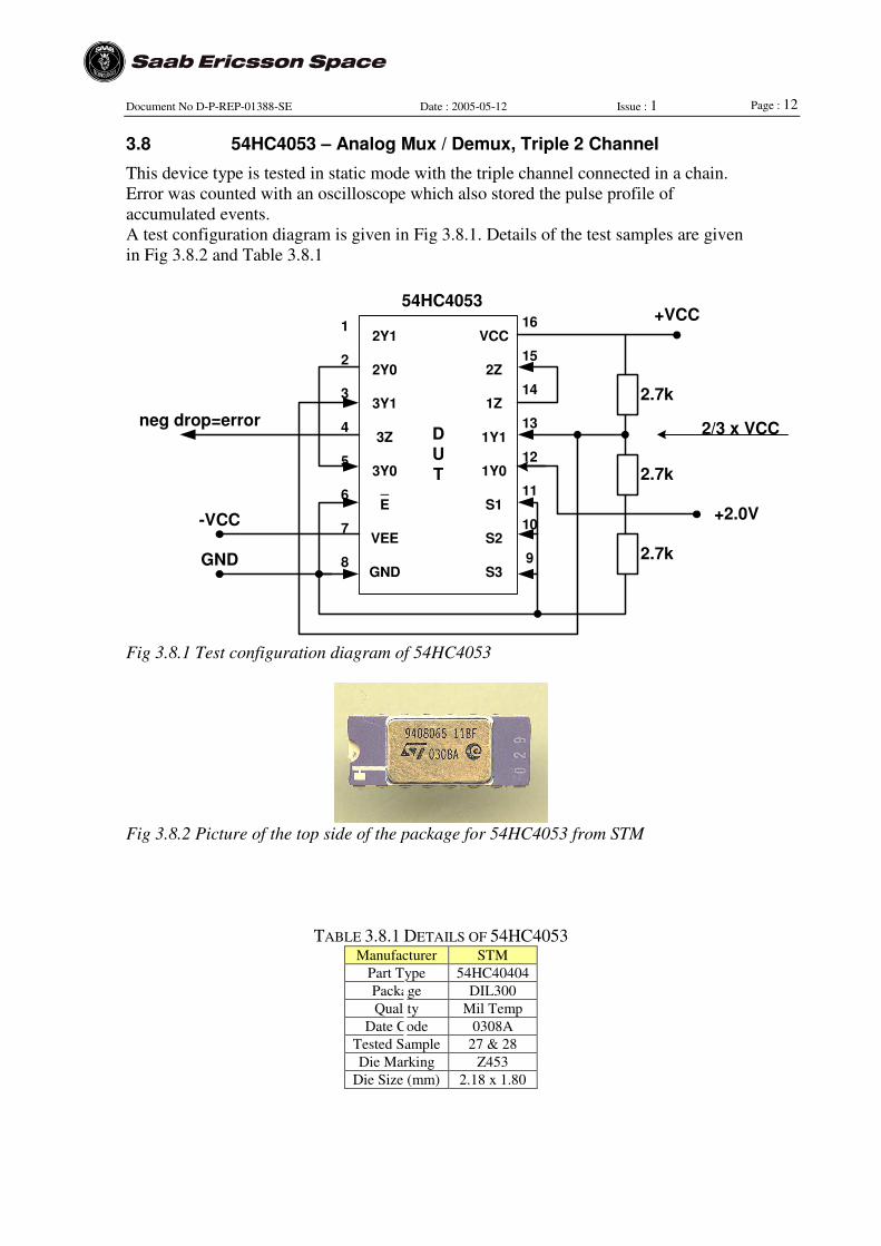
3.8 54HC4053 – Analog Mux / Demux, Triple 2 Channel
This device type is tested in static mode with the triple channel connected in a chain.
Error was counted with an oscilloscope which also stored the pulse profile of
accumulated events.
A test configuration diagram is given in Fig 3.8.1. Details of the test samples are given
in Fig 3.8.2 and Table 3.8.1
1
2
3
4
5
6
7
8
16
15
14
13
12
11
10
9GND
-VCC
2Y1
2Y0
3Y1
3Z
3Y0
_
E
VEE
GND
VCC
2Z
1Z
1Y1
1Y0
S1
S2
S3
+VCC
neg drop=errorD
U
T
54HC4053
2.7k
2.7k
2.7k
2/3 x VCC
+2.0V
Fig 3.8.1 Test configuration diagram of 54HC4053
Fig 3.8.2 Picture of the top side of the package for 54HC4053 from STM
TABLE 3.8.1 DETAILS OF 54HC4053 Manufacturer STM
Part Type 54HC40404
Package DIL300
Quality Mil Temp
Date Code 0308A
Tested Sample 27 & 28
Die Marking Z453
Die Size (mm) 2.18 x 1.80

Page : 13 Document No D-P-REP-01388-SE Date : 2005-05-12 Issue : 1
4. RESULTS
4.1 General
All device types have been tested at the three bias conditions +2.5V, +3.3V and +5V.
Two samples of each type have been tested. No single event Latch-up was observed.
Several of the types were SEU/SET insensitive to heavy ions up to maximum LET
value available. The results for these types are only summarized in Table 5.1 for worst
case voltage bias condition. Generally, the devices are working down below 2V.
Test performed on the specification limits indicated no different results from 2.5V.
TABLE 4.1 SUMMARY OF DATA FOR DEVICE TYPES WHERE NO ERROR WAS OBSERVED TO
THE MAXIMUM LET-VALUE AVAILABLE. THE RESULTS ARE ONLY GIVEN FOR 2.5V, WHICH
IS CONSIDERED TO BE WORST CASE BIAS CONDITION
Type Manufacturer LET
Effective
Fluence SEU/
SET
2,5V
Cross
Section
(MeVx
cm2/mg)
Comments
54HC08 STM 111.8 1e6 0 <1e-6
54AC08 STM 111.8 1e6 0 <1e-6
54AC08 NS 111.8 2e6 0 <5e-7
54HC157 STM 111.8 1e6 0 <1e-6
54AC157 STM 111.8 1e6 0 <1e-6
54AC157 NS 111.8 4e6 0 <2.5e-7
54AC244 STM 64.8 2e6 1 <5e-7 Tristate 1-0 *
54AC244 NS 64.8 1e6 0 <1e-6 High penetration
ions
45AC257 STM 111.8 1e6 0 <1e-6
54AC257 NS 111.8 2e6 0 <5e-7
* This error appeared immediately at beam-on and could not be repeated by new test
runs or more statistics. The error may be induced by other means than heavy ions.
4.2 Logic Circuits
The D flip/flop logic circuits represented by 54AC273 and 54HC273 indicated
increased cross section and lower threshold values with decreasing voltage. The results
are shown in Figs 4.2.1 to 4.2.3. The largest effect of decreasing voltage was observed
between 5V and 3.3V. The SEU difference between 3.3V and 2.5 were marginal in all
cases. The STM 54AC part indicated lower cross section and high threshold than
corresponding NS part. The 54HC part has significantly higher cross section than the
54AC parts, while the 54AC parts have lower threshold than the 54HC273.
The two device types 54HC273 and 54HC4040 indicated the same increase in heavy ion
sensitivity for lower bias levels, while 54HC4040 show significantly higher threshold
than 45HC273. The results for 54HC4040 are given in Fig 4.2.4.
The change in threshold value between 5V and 3.3V is generally lager than shown in
the figures due to the limited statistics. There is usually only one error in 1E6 ions/cm2
at the lowest measured LET values.

Page : 14 Document No D-P-REP-01388-SE Date : 2005-05-12 Issue : 1
54AC273 - National Semiconductor
1,E-08
1,E-07
1,E-06
1,E-05
1,E-04
10 20 30 40 50 60 70 80 90 100 110 120
LET [MeV/mg/cm2]
Cro
ss S
ecti
on
[cm
2]
54AC273NS-2.5V
54AC273NS-3.3V
54AC273NS-5.0V
Figure 4.2.1 . Cross Section versus LET value for 54AC273 from National Semiconductor.
The graph shows the average results of two tested devices. The arrow at 1E-7 MeV/mg/cm2
indicates zero measured SEU.
54AC273 - ST Microelectroics
1,E-08
1,E-07
1,E-06
1,E-05
1,E-04
10 20 30 40 50 60 70 80 90 100 110 120LET [MeV/mg/cm2]
Cro
ss S
ecti
on
[cm
2]
54AC273ST-2.5V
54AC273ST-3.3V
54AC273ST-5.0V
Figure 4.2.2 . Cross Section versus LET value for 54AC273 from ST Microelectronics. The
graph shows the average results of two tested devices.
ST Microelectronics

Page : 15 Document No D-P-REP-01388-SE Date : 2005-05-12 Issue : 1
54HC273 - ST Microelectronics
1,E-08
1,E-07
1,E-06
1,E-05
1,E-04
10 20 30 40 50 60 70 80 90 100 110 120
LET [MeV/mg/cm2]
Cro
ss S
ecti
on
[cm
2]
54HC273ST-2.5V
54HC273ST-3.3V
54HC273ST-5.0V
Figure 4.2.3 . Cross Section versus LET value for 54AC273 from ST Microelectronics. The
graph shows the average results of two tested devices.
54HC4040 - ST Miroelectronic
1.E-07
1.E-06
1.E-05
1.E-04
1.E-03
30 40 50 60 70 80 90 100 110 120
LET [MeV/mg/cm2]
Cro
ss S
ecti
on
[cm
2]
2.5V
3.3V
5.0V
Figure 4.2.4 Cross Section versus LET value for 54HC4040 from ST Microelectronics. The
graph shows the average results of two tested devices. The test results for 5V was zero at
LET=48.1 MeV/mg/cm2 and zero for 2.5V at LET=34 MeV/mg/cm
2.

Page : 16 Document No D-P-REP-01388-SE Date : 2005-05-12 Issue : 1
4.3 Analog Circuits
The analog multiplexer/demultiplexer has been tested at the three bias condition 2.5V,
3.3V and 5V using the same analog input signal at 2V. The analog device 54HC4053
indicates opposite to the digital logics the same SET sensitivity independent of bias
conditions. The cross sections for the various bias conditions are shown in Fig 4.3.1.
The SET pulse shapes for different bias conditions and different LET-values were very
similar. One example of SET pulse shape is given in Fig 4.3.2. Maximum measured
pulse width was around 200 ns.
54HC4053 - ST Microelectronic
1.E-07
1.E-06
1.E-05
1.E-04
1.E-03
10 20 30 40 50 60 70
LET [MeV/mg/cm2]
Cro
ss S
ecti
on
[cm
2]
2.5V
3.3V
5V
Figure 4.3.1 . Cross Section versus LET value for 54HC4053 from ST Microelectronics.
The graph shows the average results of two tested devices.
Figure 4.3.2 SET pulse shape for 54HC4053, LET=14 MeV/mg/cm
2, Vcc=5V

Page : 17 Document No D-P-REP-01388-SE Date : 2005-05-12 Issue : 1
5. CONCLUSION
Present data for the selected 54HC devices show very similar 5V SEU/SET behaviour
as reported in earlier tests [1] for almost 10 years ago.
The selected 54AC/54HC logic gate devices are found to be insensitive to heavy ions up
to an LET of 110 MeV/mg/cm2 (see Table 4.1 for details).
For Analog logics the SET sensitivity is not affected by the voltage level at all.
For Digital AC/HC logics, present data indicate higher susceptibility to SEU/SET when
operated at lower voltages. The relationship observed between threshold-LET and bias
voltage level varied between the digital device types. For some types the threshold
increased smoothly with increased bias, whereas others indicated more abrupt increases.
Because of these irregularities, SEU results obtained at 5V cannot safely be extrapolated
to lower voltages.

Page : 18 Document No D-P-REP-01388-SE Date : 2005-05-12 Issue : 1
6. APPENDIX
UCL 2004 April 21-22
Run# Ion Tilt (º) LET Flux Fluence Bias (V) Data Part_dev_#
5 Xe 0 55.9 3000 1.E+06 2.5 0 AC08_NS-1
7 Xe 60 111.8 3000 1.E+06 2.5 0 AC08_NS-1
8 Xe 60 111.8 3000 1.E+06 2.5 0 AC08_NS-1
9 Xe 60 111.8 3000 1.E+06 5.0 0 AC08_NS-2
10 Xe 60 111.8 3000 1.E+06 5.0 0 AC08_ST-1
11 Xe 60 111.8 3000 1.E+06 2.5 0 AC08_ST-1
12 Xe 60 111.8 3000 3.E+05 2.5 0 AC157_NS-1
13 Xe 60 111.8 3000 1.E+06 2.5 0 AC157_NS-1
14 Xe 60 111.8 3000 1.E+06 5.0 0 AC157_NS-1
15 Xe 60 111.8 3000 1.E+06 5.0 0 AC157_ST-1
16 Xe 60 111.8 3000 1.E+06 2.5 0 AC157_ST-1
17 Xe 60 111.8 3000 1.E+06 2.5 0 HC157_ST-1
18 Xe 60 111.8 3000 1.E+06 5.0 0 HC157_ST-1
19 Xe 60 111.8 3000 1.E+06 5.0 0 HC08_ST-1
20 Xe 60 111.8 3000 1.E+06 2.5 0 HC08_ST-1
21 Xe 0 55.9 4500 1.E+06 5.0 14 AC273_NS-1
23 Xe 45 79.0 4500 1.E+06 5.0 12 AC273_NS-1
24 Xe 60 111.8 3000 1.E+06 5.0 16 AC273_NS-1
25 Xe 60 111.8 3000 1.E+06 3.3 24 AC273_NS-1
26 Xe 45 79.0 4500 1.E+06 3.3 23 AC273_NS-1
27 Xe 0 55.9 6000 1.E+06 3.3 20 AC273_NS-1
28 Xe 0 55.9 5300 1.E+06 2.5 24 AC273_NS-1
29 Xe 45 79.0 5300 1.E+06 2.5 25 AC273_NS-1
30 Xe 60 111.8 5300 1.E+06 2.5 24 AC273_NS-1
40 Xe 60 111.8 3500 1.E+06 5.0 33 AC273_ST-2
41 Xe 60 111.8 3500 1.E+06 3.3 32 AC273_ST-2
42 Xe 60 111.8 3600 1.E+06 2.5 44 AC273_ST-2
43 Xe 60 111.8 4000 1.E+06 2.5 87 HC273_ST-1
44 Xe 60 111.8 4000 1.E+06 3.3 50 HC273_ST-1
45 Xe 60 111.8 4000 1.E+06 5.0 20 HC273_ST-1
46 Xe 45 79.0 4000 1.E+06 5.0 4 HC273_ST-1
47 Xe 45 79.0 3700 1.E+06 3.3 40 HC273_ST-1
48 Xe 45 79.0 4500 1.E+06 2.5 72 HC273_ST-1
49 Xe 0 55.9 6500 1.E+06 2.5 49 HC273_ST-1
50 Xe 0 55.9 6500 1.E+06 3.3 27 HC273_ST-1
51 Xe 0 55.9 6500 1.E+06 5.0 0 HC273_ST-1
Page : 19 Document No D-P-REP-01388-SE Date : 2005-05-12 Issue : 1
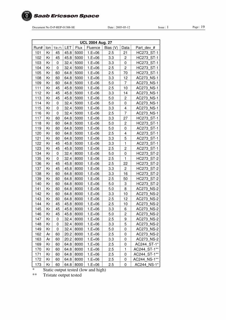
UCL 2004 Aug. 27
Run# Ion Tilt (º) LET Flux Fluence Bias (V) Data Part_dev_#
101 Kr 45 45.8 5000 1.E+06 2.5 21 HC273_ST-1
102 Kr 45 45.8 5000 1.E+06 3.3 2 HC273_ST-1
103 Kr 0 32.4 5000 1.E+06 3.3 0 HC273_ST-1
104 Kr 0 32.4 5000 1.E+06 2.5 2 HC273_ST-1
105 Kr 60 64.8 5000 1.E+06 2.5 70 HC273_ST-1
108 Kr 60 64.8 5000 1.E+06 3.3 12 AC273_NS-1
109 Kr 60 64.8 5000 1.E+06 5.0 7 AC273_NS-1
111 Kr 45 45.8 5000 1.E+06 2.5 10 AC273_NS-1
112 Kr 45 45.8 5000 1.E+06 3.3 14 AC273_NS-1
113 Kr 45 45.8 5000 1.E+06 5.0 2 AC273_NS-1
114 Kr 0 32.4 5000 1.E+06 5.0 0 AC273_NS-1
115 Kr 0 32.4 5000 1.E+06 3.3 4 AC273_NS-1
116 Kr 0 32.4 5000 1.E+06 2.5 7 AC273_NS-1
117 Kr 60 64.8 5000 1.E+06 3.3 27 HC273_ST-1
118 Kr 60 64.8 5000 1.E+06 5.0 2 HC273_ST-1
119 Kr 60 64.8 5000 1.E+06 5.0 0 AC273_ST-1
120 Kr 60 64.8 5000 1.E+06 2.5 4 AC273_ST-1
121 Kr 60 64.8 5000 1.E+06 3.3 5 AC273_ST-1
122 Kr 45 45.8 5000 1.E+06 3.3 1 AC273_ST-1
123 Kr 45 45.8 5000 1.E+06 2.5 2 AC273_ST-1
134 Kr 0 32.4 8000 1.E+06 5.0 0 HC273_ST-2
135 Kr 0 32.4 8000 1.E+06 2.5 1 HC273_ST-2
136 Kr 45 45.8 8000 1.E+06 2.5 22 HC273_ST-2
137 Kr 45 45.8 8000 1.E+06 3.3 2 HC273_ST-2
138 Kr 60 64.8 8000 1.E+06 3.3 16 HC273_ST-2
139 Kr 60 64.8 8000 1.E+06 2.5 50 HC273_ST-2
140 Kr 60 64.8 8000 1.E+06 5.0 3 HC273_ST-2
141 Kr 60 64.8 8000 1.E+06 5.0 8 AC273_NS-2
142 Kr 60 64.8 8000 1.E+06 3.3 10 AC273_NS-2
143 Kr 60 64.8 8000 1.E+06 2.5 12 AC273_NS-2
144 Kr 45 45.8 8000 1.E+06 2.5 10 AC273_NS-2
145 Kr 45 45.8 8000 1.E+06 3.3 6 AC273_NS-2
146 Kr 45 45.8 8000 1.E+06 5.0 2 AC273_NS-2
147 Kr 0 32.4 8000 1.E+06 2.5 9 AC273_NS-2
148 Kr 0 32.4 8000 1.E+06 3.3 5 AC273_NS-2
149 Kr 0 32.4 8000 1.E+06 5.0 0 AC273_NS-2
162 Ar 60 20.2 8000 1.E+06 2.5 0 AC273_NS-2
163 Ar 60 20.2 8000 1.E+06 3.3 0 AC273_NS-2
169 Kr 60 64.8 8000 1.E+06 2.5 0 AC244_ST-1*
170 Kr 60 64.8 8000 1.E+06 2.5 1 AC244_ST-1**
171 Kr 60 64.8 8000 1.E+06 2.5 0 AC244_ST-1**
172 Kr 60 64.8 8000 1.E+06 2.5 0 AC244_NS-1**
173 Kr 60 64.8 8000 1.E+06 2.5 0 AC244_NS-1*
* Static output tested (low and high)
** Tristate output tested

Page : 20 Document No D-P-REP-01388-SE Date : 2005-05-12 Issue : 1
UCL 2004 Nov. 6-7
Run# Ion Tilt (º) LET Flux Fluence Bias (V) Data Part_dev_#
173 Xe 0 55.9 3000 5.E+05 2.5 8 HC4040_ST-61
174 Xe 0 55.9 4000 5.E+05 3.3 6 HC4040_ST-61
175 Xe 0 55.9 4000 5.E+05 5.0 1 HC4040_ST-61
176 Xe 45 79.0 3500 5.E+05 5.0 6 HC4040_ST-61
177 Xe 45 79.0 3500 5.E+05 3.3 19 HC4040_ST-61
178 Xe 45 79.0 3500 5.E+05 2.5 39 HC4040_ST-61
179 Xe 60 111.8 2500 5.E+05 2.5 58 HC4040_ST-61
180 Xe 60 111.8 2500 5.E+05 3.3 33 HC4040_ST-61
181 Xe 60 111.8 2500 5.E+05 5.0 21 HC4040_ST-61
182 Xe 60 111.8 4000 5.E+05 3.3 28 HC4040_ST-62
183 Xe 60 111.8 4000 5.E+05 2.5 54 HC4040_ST-62
184 Xe 60 111.8 4000 5.E+05 5.0 14 HC4040_ST-62
185 Xe 45 79.0 6000 5.E+05 5.0 7 HC4040_ST-62
186 Xe 45 79.0 6000 5.E+05 3.3 21 HC4040_ST-62
187 Xe 45 79.0 6000 5.E+05 2.5 40 HC4040_ST-62
188 Xe 0 55.9 8000 5.E+05 2.5 21 HC4040_ST-62
189 Xe 0 55.9 8000 5.E+05 3.3 6 HC4040_ST-62
190 Xe 0 55.9 8000 5.E+05 5.0 0 HC4040_ST-62
194 Xe 0 55.9 6000 5.E+05 2.5 19 HC4040_ST-62
199 Kr 45 48.1 6000 5.E+05 2.5 8 HC4040_ST-61
200 Kr 45 48.1 6000 1.E+06 2.5 11 HC4040_ST-61
201 Kr 45 48.1 6000 1.E+06 3.3 1 HC4040_ST-61
202 Kr 45 48.1 6000 1.E+06 5.0 0 HC4040_ST-61
203 Kr 0 34.0 10000 1.E+06 2.5 0 HC4040_ST-61
204 Kr 0 34.0 10000 1.E+06 2.5 0 HC4040_ST-62
205 Kr 45 48.1 10000 1.E+06 2.5 11 HC4040_ST-62
206 Kr 45 48.1 10000 1.E+06 3.3 1 HC4040_ST-62
207 Kr 45 48.1 10000 1.E+06 5.0 0 HC4040_ST-62
213 Kr 0 34.0 8000 1.E+06 5.0 34 HC4053_ST-27
214 Kr 0 34.0 8000 1.E+06 3.3 31 HC4053_ST-27
215 Kr 0 34.0 8000 1.E+06 2.5 34 HC4053_ST-27
216 Kr 45 48.1 8000 1.E+06 2.5 37 HC4053_ST-27
217 Kr 45 48.1 8000 1.E+06 3.3 47 HC4053_ST-27
220 Kr 45 48.1 8000 1.E+06 5.0 34 HC4053_ST-27
222 Kr 45 48.1 8000 1.E+06 5.0 47 HC4053_ST-28
223 Kr 45 48.1 7500 1.E+06 3.3 48 HC4053_ST-28
225 Kr 0 34.0 8000 1.E+06 2.5 45 HC4053_ST-28
226 Kr 0 34.0 8000 1.E+06 3.3 33 HC4053_ST-28
227 Kr 0 34.0 8000 1.E+06 5.0 22 HC4053_ST-28
228 Kr 60 68.0 8000 1.E+06 5.0 72 HC4053_ST-28
229 Kr 60 68.0 8000 1.E+06 3.3 82 HC4053_ST-28
230 Kr 60 68.0 8000 1.E+06 2.5 79 HC4053_ST-28
235 Kr 60 68.0 8000 1.E+06 2.5 94 HC4053_ST-27
236 Kr 60 68.0 8000 1.E+06 3.3 82 HC4053_ST-27
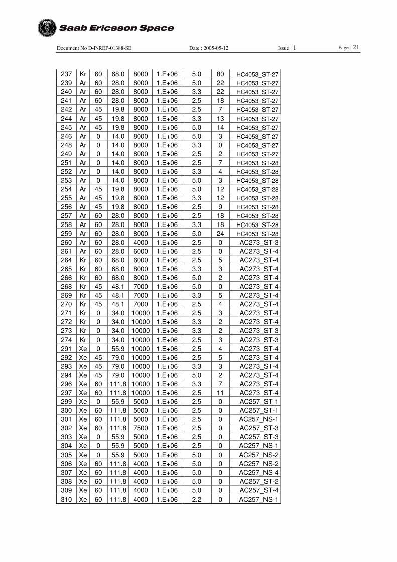
Page : 21 Document No D-P-REP-01388-SE Date : 2005-05-12 Issue : 1
237 Kr 60 68.0 8000 1.E+06 5.0 80 HC4053_ST-27
239 Ar 60 28.0 8000 1.E+06 5.0 22 HC4053_ST-27
240 Ar 60 28.0 8000 1.E+06 3.3 22 HC4053_ST-27
241 Ar 60 28.0 8000 1.E+06 2.5 18 HC4053_ST-27
242 Ar 45 19.8 8000 1.E+06 2.5 7 HC4053_ST-27
244 Ar 45 19.8 8000 1.E+06 3.3 13 HC4053_ST-27
245 Ar 45 19.8 8000 1.E+06 5.0 14 HC4053_ST-27
246 Ar 0 14.0 8000 1.E+06 5.0 3 HC4053_ST-27
248 Ar 0 14.0 8000 1.E+06 3.3 0 HC4053_ST-27
249 Ar 0 14.0 8000 1.E+06 2.5 2 HC4053_ST-27
251 Ar 0 14.0 8000 1.E+06 2.5 7 HC4053_ST-28
252 Ar 0 14.0 8000 1.E+06 3.3 4 HC4053_ST-28
253 Ar 0 14.0 8000 1.E+06 5.0 3 HC4053_ST-28
254 Ar 45 19.8 8000 1.E+06 5.0 12 HC4053_ST-28
255 Ar 45 19.8 8000 1.E+06 3.3 12 HC4053_ST-28
256 Ar 45 19.8 8000 1.E+06 2.5 9 HC4053_ST-28
257 Ar 60 28.0 8000 1.E+06 2.5 18 HC4053_ST-28
258 Ar 60 28.0 8000 1.E+06 3.3 18 HC4053_ST-28
259 Ar 60 28.0 8000 1.E+06 5.0 24 HC4053_ST-28
260 Ar 60 28.0 4000 1.E+06 2.5 0 AC273_ST-3
261 Ar 60 28.0 6000 1.E+06 2.5 0 AC273_ST-4
264 Kr 60 68.0 6000 1.E+06 2.5 5 AC273_ST-4
265 Kr 60 68.0 8000 1.E+06 3.3 3 AC273_ST-4
266 Kr 60 68.0 8000 1.E+06 5.0 2 AC273_ST-4
268 Kr 45 48.1 7000 1.E+06 5.0 0 AC273_ST-4
269 Kr 45 48.1 7000 1.E+06 3.3 5 AC273_ST-4
270 Kr 45 48.1 7000 1.E+06 2.5 4 AC273_ST-4
271 Kr 0 34.0 10000 1.E+06 2.5 3 AC273_ST-4
272 Kr 0 34.0 10000 1.E+06 3.3 2 AC273_ST-4
273 Kr 0 34.0 10000 1.E+06 3.3 2 AC273_ST-3
274 Kr 0 34.0 10000 1.E+06 2.5 3 AC273_ST-3
291 Xe 0 55.9 10000 1.E+06 2.5 4 AC273_ST-4
292 Xe 45 79.0 10000 1.E+06 2.5 5 AC273_ST-4
293 Xe 45 79.0 10000 1.E+06 3.3 3 AC273_ST-4
294 Xe 45 79.0 10000 1.E+06 5.0 2 AC273_ST-4
296 Xe 60 111.8 10000 1.E+06 3.3 7 AC273_ST-4
297 Xe 60 111.8 10000 1.E+06 2.5 11 AC273_ST-4
299 Xe 0 55.9 5000 1.E+06 2.5 0 AC257_ST-1
300 Xe 60 111.8 5000 1.E+06 2.5 0 AC257_ST-1
301 Xe 60 111.8 5000 1.E+06 2.5 0 AC257_NS-1
302 Xe 60 111.8 7500 1.E+06 2.5 0 AC257_ST-3
303 Xe 0 55.9 5000 1.E+06 2.5 0 AC257_ST-3
304 Xe 0 55.9 5000 1.E+06 2.5 0 AC257_NS-1
305 Xe 0 55.9 5000 1.E+06 5.0 0 AC257_NS-2
306 Xe 60 111.8 4000 1.E+06 5.0 0 AC257_NS-2
307 Xe 60 111.8 4000 1.E+06 5.0 0 AC257_NS-4
308 Xe 60 111.8 4000 1.E+06 5.0 0 AC257_ST-2
309 Xe 60 111.8 4000 1.E+06 5.0 0 AC257_ST-4
310 Xe 60 111.8 4000 1.E+06 2.2 0 AC257_NS-1