project overview
TRANSCRIPT
SUBMISSION OF PROJECT
IC CONTROLLED EMERGENCY LIGHT WITH CHARGER
IN PARTIAL FULLFILLMENT OF SUBJECT
ELECTRONIC DEVICES AND CIRCUIT 1 & ELECTRONIC DEVICES AND CIRCUIT 2
NAME OF PROJECT MEMBERS:
SWATI KAMATH AFSHAN KHAN
JAYESH KAMAT PRINCE MODI
PROJECT GUIDENCE PROJECT INCHARGE

CONTENTS
ABSTRACT
CIRCUIT DIAGRAM
WORKING OF CIRCUIT
SPECIFICATION OF COMPONENTS
DETAILS OF IC’S
APPLICATIONS AND FURTHER MODIFICATIONS
REPLACEMENT OF SUBSTITUTE IC AND DETAILS OF SUBSTITUTE IC
ACKNOWLEDGEMENT
REFERENCES
ABSTRACT
The circuit shown here is that of the IC Controlled Emergency Light
With Charger. Its main features are: Automatic Switching- on of the
lights when mains fails and battery charger with overcharge protection.
When mains is absent, the relay is de-energised, feeding battery supply
to the inverter section. The inverter section consists of IC-555 which is
used in stable mode to produce sharp pulses for driving the mosfet. The
power amplifier built across mosfet functions in push pull mode. Finally
transformer is used to drive a 230v fluorescent tube.
CIRCUIT DIAGRAM
WORKING OF THE CIRCUIT
The circuit shown here is of IC controlled emergency light with charger. Its main features are: switching-on of light when mains failure occurs and battery charger with over voltage protection.
When mains is absent, relay RL2 is in de-energised state, feeding batter supply to inverter section via its NC contacts and switch S1. The inverter section comprises of IC2 (NE-555) which is used in stable mode to produce sharp pulses at the rate of 50Hz for driving of mosfet. The o/p of IC3 is fed to gate of mosfet (T4) directly while it is applied to mosfet (T3) gate after inversion by transistor T2. Thus the power amplifier built around mosfet T3 and T4 acts as push pull amplifier.
The output across secondary of transformer X2 can easily drive a 230V, 20 watt fluorescent tube. In case light is not required to be on during mains failure, simply flip switch S1 to off position.
Battery overcharge protection circuit is built around IC LM-308. Its Non-inverting pin is held at a reference voltage at approximately 6.9V which is obtained using diode D5 (1N4148) and 6.2V zener D6. The inverting pin of IC1 is connected to positive terminal of battery. Thus when the mains supply is present, IC1 comparator output is high, unless battery

voltage exceeds 6.9V. So transistor T1 is normally forward biased, which energizes relay RL1. In this state the relay battery remains on charge via N/O contacts of relay RL1 and current limiting resistor R2. When battery voltage exceeds 6.9V(over charge condition), IC1 output goes low and relay RL1 gets de-energized, and thus stops the further charging of the battery.
Mosfet’s T3 and T4 can be mounted on suitable Heat Sinks.

Specifications of the components
Details of ic’s
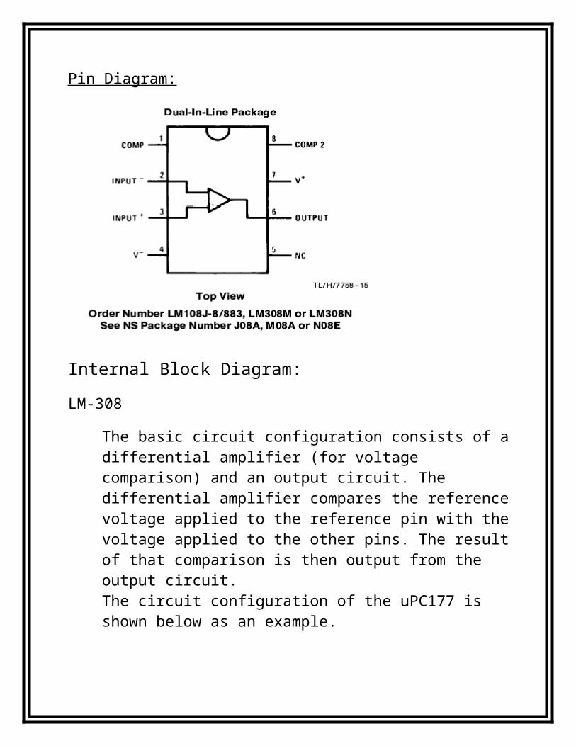
Lm-308:
Pin Diagram:
Internal Block Diagram:
LM-308
The basic circuit configuration consists of a differential amplifier (for voltage comparison) and an output circuit. The differential amplifier compares the reference voltage applied to the reference pin with the voltage applied to the other pins. The result of that comparison is then output from the output circuit. The circuit configuration of the uPC177 is shown below as an

example.
Working:
The LM308 series are precision operational amplifiers havingspecifications a factor of ten better than FET amplifiersover a -55C to a125C temperature range.The devices operate with supply voltages from 2V to±20V and have sufficient supply rejection to use unregulatedsupplies.
Mode Of Operation:
LM-308-COMPARATOR MODE
A ‘comparator’ is an circuit that compares two input voltages. One voltage is called the reference voltage (Vref) and the other is called the input voltage (Vin).
When Vin rises above or falls below Vref the output changes polarity (+ becomes -).

Positive is sometimes called HIGH.Negative is sometimes called LOW.
Application in our Project:
It is used to energize or de-energize relay.
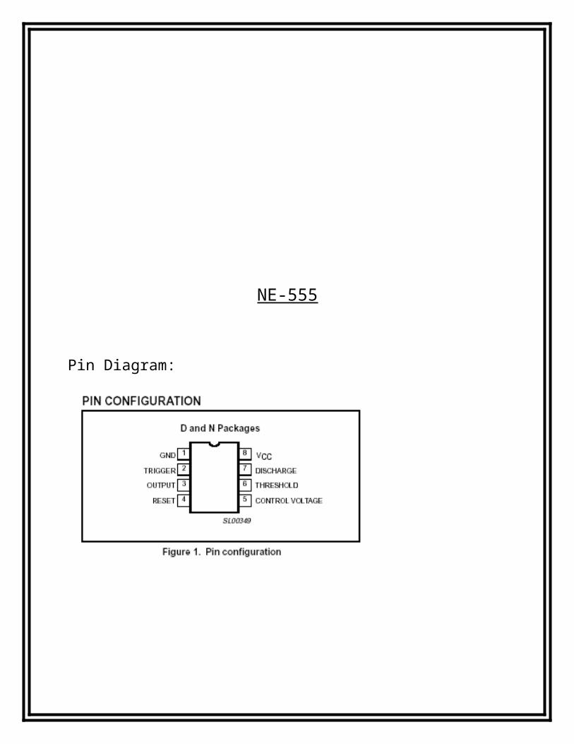
NE-555
Pin Diagram:

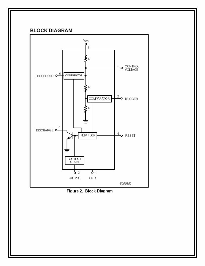
Internal Block Diagram:

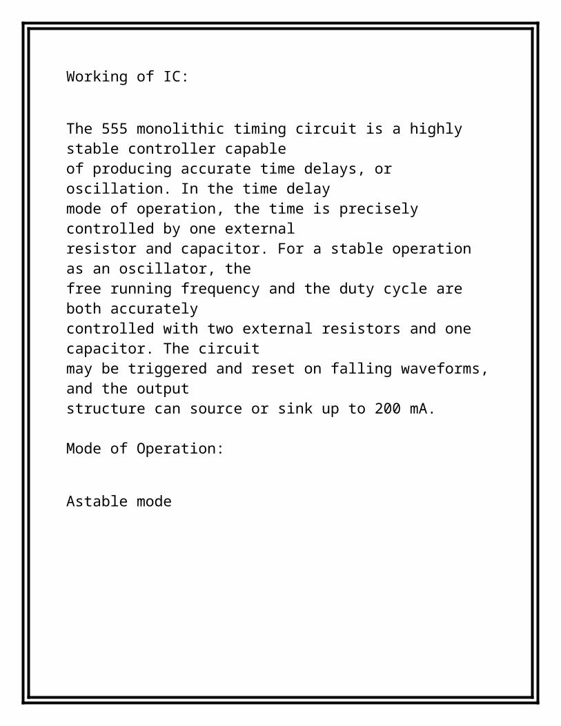
Working of IC:
The 555 monolithic timing circuit is a highly stable controller capableof producing accurate time delays, or oscillation. In the time delaymode of operation, the time is precisely controlled by one externalresistor and capacitor. For a stable operation as an oscillator, thefree running frequency and the duty cycle are both accuratelycontrolled with two external resistors and one capacitor. The circuitmay be triggered and reset on falling waveforms, and the outputstructure can source or sink up to 200 mA.
Mode of Operation:
Astable mode
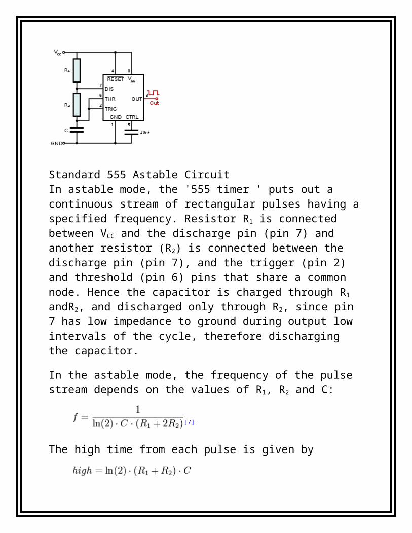
Standard 555 Astable CircuitIn astable mode, the '555 timer ' puts out a continuous stream of rectangular pulses having a specified frequency. Resistor R1 is connected between VCC and the discharge pin (pin 7) and another
resistor (R2) is connected between the discharge pin (pin 7), and the trigger (pin 2) and threshold (pin 6) pins that share a common node. Hence the capacitor is charged through R1 andR2, and discharged only through R2, since pin 7 has low impedance to ground during output low intervals of the cycle, therefore discharging the capacitor.
In the astable mode, the frequency of the pulse stream depends on the values of R1, R2 and C:
[7]
The high time from each pulse is given by
and the low time from each pulse is given by
Application of IC in project:
IC 555 which is used in stable mode to produce sharp pulse for driving the MOSFET

APPLICATIONS:
The project has a very wide scope of application in every day human world. It does not matter whether it is your home, office or your factory. This project can be used everywhere.
As soon as the Mains will fail, the project will do its work by providing Light. This project will never let you stay in dark.
This project can also run Fans, Motors, etc. provided the proper battery supply.
Replacement IC:
LM-108:
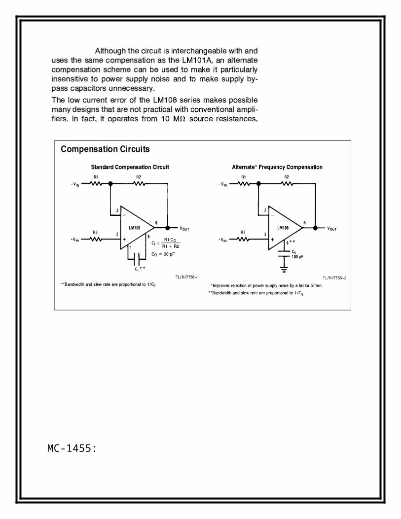
MC-1455:
The MC1455 monolithic timing circuit is a highly stable controller capable of producing accurate time delays or oscillation. Additional terminals are provided for triggering or resetting if desired. In the time delay mode, time is precisely controlled by one external resistor and capacitor. For astable operation as an oscillator, the free–running frequency and the duty cycle are both accurately controlled with two external resistors and one capacitor. The circuit may be triggered and reset on falling waveforms, and the output structure can source or sink up to 200 mA or drive MTTL circuits.
Direct Replacement for NE555 TimersTiming from Microseconds through HoursOperates in Both Astable and Monostable ModesAdjustable Duty CycleHigh Current Output Can Source or Sink 200 mAOutput Can Drive MTTLTemperature Stability of 0.005% per CNormally ON or Normally OFF Output117 Vac/60 Hz
Working:
In the astable mode the timer is connected so that it willretrigger itself and cause the capacitor voltage to oscillatebetween 1/3 VCC and 2/3 VCC. See Figure 17.The external capacitor changes to 2/3 VCC through RA andRB and discharges to 1/3 VCC through RB. By varying the ratioof these resistors the duty cycle can be varied. The charge anddischarge times are independent of the supply voltage.The charge time (output high) is given by:t1 = 0.695 (RA + RB) CThe discharge time (output low) is given by:t2 = 0.695 (RB) CThus the total period is given by:T = t1 + t2 = 0.695 (RA +2RB) C
The frequency of oscillation is then:

f = I/T=1.44/ (RA +2RB) C
and may be easily found as shown in Figure 19.The duty cycle is given by:
DC =
To obtain the maximum duty cycle RA must be as small asPossible.

Acknowledgement
It is a great pleasure of mine and sense of satisfaction to present my first endeavourer in practical computing – this project work.
I would take this opportunity to thank every possible reason that made the project success. Firstly, I thank Mumbai University, for including such a project activity for students in the S.Y.E.X.T.C. curriculum that actually gave me an opportunity to understand the aspects of working in a Electronics industry.
I would thank all my teachers till date, who has always been there to guide me to select the right path, encourage me to work harder, impart skills in me to work smarter. Specially, I would like to thank Mrs. Sonia Behra, my project guide at Thakur College of Engg. & Tech. for her constant guidance.
I thank the entire Electronics & Telecommunication department, who has helped me in completing my project successfully. I as very grateful to my Team partners for their co-operation and guidance. My colleagues are appreciated for their support. All are gratefully thanked for their guidance and teaching. I am specially thanking Electronics & Telecommunication department for giving me opportunity to learn and grow in knowledge. I thank my family and friends for all the support they have given me to be at place where I am today.
Without the support of all these people this would have not been possible.
Thanks to all again.
Prince Modi, Swati Kamath, Jayesh Kamat, Afshan Khan.
References
Basic Electronics – B.Ram
Digital Electronics – R.P.Jain
www.alldatasheet.com
http://www.electronicsforu.com