provably-secure logic locking: from theory to practice · provably-secure logic locking: from...
TRANSCRIPT

Provably-Secure Logic Locking: From Theory To PracticeMuhammad Yasin
New York University, New York, USA
Abhrajit Sengupta
New York University, New York, USA
Mohammed �ari Nabeel
New York University Abu Dhabi, UAE
Mohammed Ashraf
New York University Abu Dhabi, UAE
Jeyavijayan (JV) Rajendran
�e University of Texas at Dallas/
Texas A&M University, Texas, USA
Ozgur Sinanoglu
New York University Abu Dhabi, UAE
ABSTRACTLogic locking has been conceived as a promising proactive defense
strategy against intellectual property (IP) piracy, counterfeiting,
hardware Trojans, reverse engineering, and overbuilding a�acks.
Yet, various a�acks that use a working chip as an oracle have been
launched on logic locking to successfully retrieve its secret key,
undermining the defense of all existing locking techniques. In
this paper, we propose stripped-functionality logic locking (SFLL),
which strips some of the functionality of the design and hides it in
the form of a secret key(s), thereby rendering on-chip implementa-
tion functionally di�erent from the original one. When loaded onto
an on-chip memory, the secret keys restore the original functional-
ity of the design. �rough security-aware synthesis that creates a
controllable mismatch between the reverse-engineered netlist and
original design, SFLL provides a quanti�able and provable resilience
trade-o� between all known and anticipated a�acks. We demon-
strate the application of SFLL to large designs (>100K gates) using
a computer-aided design (CAD) framework that ensures a�aining
the desired security level at minimal implementation cost, 8%, 5%,
and 0.5% for area, power, and delay, respectively. In addition to
theoretical proofs and simulation con�rmation of SFLL’s security,
we also report results from the silicon implementation of SFLL on
an ARM Cortex-M0 microprocessor in 65nm technology.
CCS CONCEPTS•Security and privacy →Security in hardware; Hardware at-tacks and countermeasures; Hardware reverse engineering;Hardware security implementation; •Hardware →Logic synthe-sis; Electronic design automation;
KEYWORDSDesign-for-trust, IP piracy, hardware Trojan, reverse engineering,
logic locking, Boolean satis�ability (SAT)
Permission to make digital or hard copies of all or part of this work for personal or
classroom use is granted without fee provided that copies are not made or distributed
for pro�t or commercial advantage and that copies bear this notice and the full citation
on the �rst page. Copyrights for components of this work owned by others than ACM
must be honored. Abstracting with credit is permi�ed. To copy otherwise, or republish,
to post on servers or to redistribute to lists, requires prior speci�c permission and/or a
fee. Request permissions from [email protected].
CCS’17, Oct. 30–Nov. 3, 2017, Dallas, TX, USA.© 2017 ACM. ISBN 978-1-4503-4946-8/17/10. . .$15.00
DOI: h�p://dx.doi.org/10:1145/3133956:3133985
Tamper-proof
memory
Inputs OutputsCircuit to be
protected
Key inputs
Figure 1: An abstract representation of a logic-locked design.Only on applying the secret key, the design produces correctoutputs; otherwise, incorrect outputs are produced.
1 INTRODUCTION1.1 IP piracy and reverse engineering�e increasing cost of IC manufacturing has forced many com-
panies to go fabless over the years. With the outsourcing of IC
fabrication in a globalized/distributed design �ow including multi-
ple (potentially untrusted) entities, the semiconductor industry is
facing a number of challenging security threats. �is fragility in
the face of poor state-of-the-art IP protection has resulted in hard-
ware security vulnerabilities such as IP piracy, overbuilding, reverse
engineering, and hardware Trojans [9, 13, 19, 20, 37, 39, 45, 47–49].
To address these issues most e�ectively at the hardware level [32],
a number of hardware design-for-trust (DfTr) techniques such as
IC metering [1, 22, 23], watermarking [17, 18, 21, 31], IC camou�ag-
ing [3, 4, 27, 28, 35, 46, 51, 56, 62], split manufacturing [14, 16], and
logic locking [34, 36, 38, 40, 41, 52, 53, 55, 61, 63] have been pro-
posed. Logic locking, in particular, has received signi�cant interest
from the research community, as it can protect against a potential
a�acker located anywhere in the IC supply chain, whereas other
DfTr techniques such as camou�aging or split manufacturing can
protect only against a limited set of malicious entities as shown
in Table 1. Mentor Graphics, a major CAD tool provider, has an-
nounced the launch of TrustChain, a framework to support logic
locking and camou�aging [26, 42].
1.2 Logic locking: defenses and attacksLogic locking inserts additional logic into a circuit, locking the
original design with a secret key. In addition to the original in-
puts, a locked circuit has key inputs that are driven by an on-chip
tamper-proof memory [15, 50], as illustrated in Fig. 1. �e addi-
tional logic may consist of XOR gates [34, 36, 38] or look-up tables
(LUTs) [5]. Fig. 2 presents the IC design �ow incorporating logic
locking. �e locked netlist passes through the untrusted design
phases. Without the secret key (i) the design details cannot be
recovered (for reverse-engineering), and (ii) the IC is not functional,
Session G5: Hardening Hardware CCS’17, October 30-November 3, 2017, Dallas, TX, USA
1601

Logic
synthesis
Logic
lockingFabrication
Original
netlist
Physical
synthesisLocked
netlistLayout Activation
Functional
ICSystem
specs.
Test/
packaging
Locked
IC
Figure 2: Locking and activation of an IC in IC design �ow. �e red regions denote untrusted entities; the green regionsrepresent trusted entities.
Table 1: Protection o�ered by DfTr techniques against un-trusted entities in the IC supply chain.
Techniques Foundry SoC Integrator Test UserIC metering [1, 22, 23] 7 3 3 3
Watermarking [17, 18, 21, 31] 7 7 7 3
IC camou�aging [3, 4, 27, 28, 35, 46, 51] 7 3 3 3
Split manufacturing [14, 16] 3 7 7 7
Logic locking [34, 36, 38, 52, 55] 3 3 3 3
i.e., it produces incorrect outputs (for over-production). A locked
IC needs to be activated by loading the secret key onto the chip’s
memory.
Traditional logic locking techniques choose key gate loca-
tions based on various gate selection algorithms, such as ran-
dom (RLL) [38], fault analysis-based (FLL) [5, 36], and strong-
interference-based logic locking (SLL) [34, 59]. Over the years,
many key-recovery a�acks have been mounted that exploit the
vulnerabilities of logic locking techniques [33, 34, 44, 54, 60]. A
summary of these a�acks is presented in Table 2.
A powerful a�ack that broke all the logic locking techniques
existing then is Boolean satis�ability (SAT)-based key-pruning a�ack,
referred to as SAT a�ack. �e a�ack is based on the notion of incor-rect key elimination using distinguishing input pa�erns (DIPs) [44].
DIPs are computed using a miter circuit constructed using two
copies of the locked netlist; the two circuits share the primary
inputs but have di�erent key inputs. A DIP is found when the
two copies of the locked netlist di�er in their outputs. A func-
tional IC with the secret key loaded in its memory is used as an
oracle to identify the incorrect keys in an iterative fashion. �e
computational complexity of the a�ack is expressed in terms of
the number of DIPs generated by the SAT a�ack [44]. �e latest
research works on logic locking have focused on defending against
the SAT a�ack [52, 55, 57].
1.3 SAT attack resilient logic lockingTwo SAT a�ack resilient logic locking techniques—SARLock [55]
and Anti-SAT [52] (see Fig. 3)—have been recently proposed. �ey
both use one-point functions to obtain resilience against SAT at-
tacks. SARLock corrupts/inverts the output of the circuit for all the
incorrect keys at exactly one input pa�ern that is di�erent for each
incorrect key. �e correct key values are hardcoded in logic gates
to mask the output inversion for the correct key [55]. Anti-SAT
employs two complementary logic blocks that converge at an AND
gate. �e output of the AND gate is always 0 only for the correct
Table 2: Attack resiliency of logic locking techniquesagainst the existing attacks. 7 denotes susceptibility to theattack and 3 denotes resilience.
A�ack RLL FLL SLL AntiSAT SARLock TTLock Proposed
[38] [5, 36] [34] [52] [55] [61] SFLL
Sensitization [34] 7 7 3 3 3 3 3SAT [44] 7 7 7 3 3 3 3
AppSAT [40] 7 7 7 7 7 7 3Removal/SPS [57] 3 3 3 7 7 3 3
Original circuitIN OUT
G(X,Kl1)
G(X,Kl2)
X
Kl1
Kl2
Original circuit
?= Mask
OUTFlip
IN
K
Flip
(a) (b)
Tamper-proof memory
Tamper-proof memory
Figure 3: (a) SARLock [55]. (b) Anti-SAT [52]. In both tech-niques, an incorrect key may assert the flip signal, produc-ing incorrect outputs. Source: [61].
key; otherwise, it may be 1. Its output corrupts an internal node
in the original design for an incorrect key, to produce incorrect
outputs.
SARLock can be intertwined with one of the gate selection-
based logic locking techniques, such as RLL, FLL or SLL, providing
multiple layers of defense [55]. A variant of SAT a�ack, referred to
as AppSAT [40], was recently proposed to show that a multi-layered
defense comprising a point function and a SAT a�ack vulnerable
logic locking technique can be reduced to a single-layer defense
comprising the point function alone (e.g., from SARLock+FLL to
SARLock). �e Double-DIP a�ack achieves the same objective
using more powerful 2-DIPs, i.e., DIPs that can eliminate at least
two incorrect keys in a single iteration [41]. �e work in [40, 41]
elucidates that simple integration of multiple techniques together
fails to combine the resilience o�ered by individual techniques.
Limitations of existingwork: Protection unit that can be iso-lated and removed. Despite their SAT a�ack resilience, both
SARLock [55] and Anti-SAT [52] exhibit security vulnerabilities,
as they leave the original circuit implementation, the IP-to-be-
protected, as is. SARLock is vulnerable to removal a�ack: Given
a protected/locked netlist, an a�acker can identify the compara-
tor/mask blocks and the �ip signal that directly feeds the output
by tracing the transitive-fanout of key-inputs, and remove these
blocks, retrieving the original circuit (proprietary IP). Anti-SAT
is vulnerable to signal probability skew (SPS) a�ack [57]: Given a
protected netlist, an a�acker can identify the �ip signal: it is at
the output of the gate whose inputs exhibit the maximum bias
towards opposite values. �e a�acker can then retrieve the origi-
nal design by re-synthesizing the locked netlist with a constraint
value 0 (1) on the �ip signal. Even upon additional obfuscation
using additional XOR/XNOR and multiplexer key gates [52], the
Anti-SAT block can be isolated using the AppSAT guided removal
(AGR) a�ack [58]. In addition, both SARLock and Anti-SAT are
also vulnerable to the Bypass a�ack [53]. �e Bypass a�ack �nds
a DIP that causes an incorrect output for a wrong key and bypass
circuitry is added around the Anti-SAT/SARLock block to �x the
output for this DIP. �is �x recovers the original design as for both
SARLock and Anti-SAT the incorrect key-driven design fails for
only one input pa�ern.
SARLock is re-architected into TTLock in [61] to gain resilience
against removal a�acks. TTLock makes changes to the original
Session G5: Hardening Hardware CCS’17, October 30-November 3, 2017, Dallas, TX, USA
1602

design to corrupt the output in the absence of the secret key. As
SARLock is based on a one-point function, its re-architected version
TTLock ends up protecting one input pa�ern, that is, the modi�ed
netlist and the original netlist di�er in their outputs for one input
pa�ern only. �e work in [61] describes this SAT and removal
a�ack resilient architecture but provides neither a CAD framework
to e�ect the design changes nor a formal analysis proving resilience
against various a�acks. Furthermore, protection of a single input
pa�ern leads to a rigid scheme where the designer lacks the control
to hide an arbitrary amount of IP-critical logic in arbitrary parts
of his/her design. Protection of a single input pa�ern, and thus,
low (and uncontrollable) corruptibility also leads to the recovery of
an approximate netlist through a�acks, such as AppSAT [40] and
Double-DIP [41], which SARLock is vulnerable to as well.
1.4 Motivation, proposed approach, andchallenges
Motivation. Our ultimate goal is to develop a logic locking tech-
nique that can withstand all known and anticipated a�acks. Re-
silience to oracle-guided a�acks, such as SAT a�ack, should be
delivered while at the same time hardware implementation of the
design should not reveal all the details of the design IP to reverse-
engineers (i.e., removal a�acks). A logic locking framework should
enable the designer to hide the security-critical parts of the design
IP, and thereby, to customize logic locking to the security needs of
the application.
While hiding any part of the design IP from its hardware imple-
mentation may be su�cient to render general applications resilient
to reverse engineers (removal a�acks), there are applications where
a designer may want to specify the parts to hide. Examples in-
clude processors with to-be-protected address spaces, for which
access is granted only to restricted entities [8]; network-on-chip
(NoC) routers where certain IP address ranges may carry particular
semantics [12]; intrusion detection systems that rely on pa�ern
matching [24]; and digital signal processing applications, such as
comb �lters [10], which accentuate/a�enuate frequencies at regular
intervals.
Approach. Building on the architecture abstracted in [61], the
proposed technique strips part of the design functionality from
its hardware implementation. �e design implemented in hard-
ware is therefore no longer the same as the original design, as
the former will be missing the stripped functionality. We refer to
the proposed technique that can arbitrarily specify this stripped
functionality as Stripped-Functionality Logic Locking (SFLL). �e
hardware implementation can be conceived to have an intentionally
and controllable built-in error. �is error is canceled by a restoreunit only upon the application of the secret key of logic locking.
�e stripped functionality can be captured e�ciently in terms
of input cubes1
for which the hardware-implemented design and
the original one produce di�erent outputs. We refer to these input
cubes as protected cubes. �ey can be stored in bits rather than
hardcoded in logic gates. SARLock [55] and Anti-SAT [52] protect
zero cubes, as they implement the design IP as is in hardware.
1Input cubes refer to partially-speci�ed input pa�erns; some input bits are set to
logic-0’s or logic-1’s, while other input bits are don‘t cares (x’s). An n-bit input cube
with k speci�ed (care) bits contains 2n−k
input pa�erns.
Protected cubes can also be conceived as conditions to manifest the
built-in error; a reverse-engineer applying the removal a�ack will
obtain a netlist with this error with respect to the original design.
For general applications that require hiding any part of the func-
tionality, it may be su�cient to protect an arbitrary set of cubes. For
applications that are speci�c about the part of the functionality to
hide, the proposed SFLL framework should enable the designer to
strip functionality based on IP-critical cubes that he/she can specify
and provide as input to the framework.
Challenges. �e proposed approach necessitates that we dis-
cover and explore the connection between resilience to oracle-
guided a�acks and removal a�acks. �is translates to another
challenge–quantifying the resilience of logic locking to a�acks in
terms of properties (e.g., the number and size) of cubes protected by
them. Only then, we can implement a logic locking framework that
can enable the designer to make an informed decision on how to
trade resilience to one a�ack for resilience to another, and identify
the sweet spot to protect against all a�acks.
1.5 Contributions• We discover, quantify, and explore the trade-o� between re-
silience of logic locking to di�erent a�acks.
• We develop a provably and quanti�ably secure and scalable logic
locking technique SFLL that thwarts all known and anticipated
a�acks. We present two versions of SFLL.
(1) �e �rst version SFLL-HDh , a generalized version of TT-
Lock [61], is suitable for general application where stripping
an arbitrary part of the functionality is su�cient for pro-
tection. �is implementation is simple and scalable but is
capable of protecting a restricted set of input cubes, all dic-
tated by one secret key. SFLL-HDh
protects
(kh)
input cubes
that are of Hamming Distance (HD) h from the k-bit secret
key. We provide a security analysis and show that k and hdictate the trade-o� between oracle-guided a�ack resilience
and removal a�ack resilience.
(2) �e second version SFLL-�exc×k allows the user to specify cIP-critical input cubes to be protected, each with k speci�ed
bits.
– We quantify the security level and trade-o� in terms
of the number and the size of these cubes.
– We develop a two-stage optimization framework that i)
compresses the input cubes, and ii) performs security-
aware logic synthesis to strip functionality based on
compressed cubes while lowering the cost of imple-
mentation and adhering to security requirements.
• �is is a complete approach from theory to practice. We develop
security de�nitions and metrics; develop a CAD framework for
SFLL; and validate SFLL’s security, cost-e�ectiveness, and scala-
bility through both computer simulations on large-sized bench-
mark circuits (one with >100K gates) and silicon implementation
of ARM Cortex-M0 microprocessor in 65nm LPe technology. We
fabricate both the baseline and the SFLL-locked microprocessors to
perform an accurate comparative analysis.
Session G5: Hardening Hardware CCS’17, October 30-November 3, 2017, Dallas, TX, USA
1603

2 PRELIMINARIESBefore delving into further details, we �rst de�ne the terminologies
that are used in the remainder of the paper.
Notation. We de�ne a set as S and its elements are denoted as
s ∈ S. We write s$←− S to denote s has been sampled uniformly
randomly from the set S. We use cktlock , cktactv and cktr ec to
denote a logic-locked, an activated, and a reconstructed circuit,
respectively. For a circuit ckt the set of all possible inputs and
outputs are denoted as I andO respectively. We writeAS to denote
a probabilistic polynomial time (PPT) adversary A following an
a�ack strategy S.
De�nition 2.1. A combinational circuit ckt is a netlist that im-
plements a Boolean function F : I → O , where I = {0, 1}n and
O = {0, 1}m with n inputs and m outputs. A logic locking tech-
nique L can be viewed as a triplet of algorithms, (Gen, Lock,Activate), where:
(1) Gen is a randomized key generation algorithm, z$←−
Gen(1k ), where k denotes the key-size,
(2) Lock is the algorithm to lock a circuit’s functionality,
cktlock ← Lockz (ckt), and
(3) Activate is a deterministic algorithm that activates the
locked circuit, cktactv ← Activatez (cktlock ) such that
∀i ∈ I , cktactv (i) = F (i).
�reat model. Consistent with the previous works, here we as-
sume the a�acker has access to an oracle, denoted, ckt(·), which
is a copy of a working chip with the secret key loaded onto its
memory. �e a�acker queries the oracle with a set of input pat-
terns and observes the corresponding outputs. Apart from this, the
a�acker also has the reverse-engineered netlist cktlock , which is
locked using a logic locking technique L. In this work, we assume
the a�acker also knows the corresponding elements between the
original and the locked netlist; that is, he can identify the location
of the protection unit. �e a�ack success for an adversary ASimplies recovering a circuit such that:
∀i ∈ I , cktr ec (i) = F (i), AS : cktlock → cktr ec (1)
SAT attack resilience. SAT a�ack, a representative and e�ective
oracle-guided a�ack that iteratively prunes the key space, queries
the oracle cktlock (·)with an input pa�ern d , called a distinguishing
input pa�ern, to eliminate a set of incorrect keys in each iteration.
�e a�ack terminates a�er querying the oracle with a set of DIPs,
and outpu�ing a single key z′. �e a�acker ASAT reconstructs
a circuit cktr ec where cktr ec ← Activatez′(cktlock ) such that Eq.
(1) is satis�ed.
De�nition 2.2. A logic locking technique L is called λ-secure
against a PPT adversary ASAT, making a polynomial number of
queries q(λ) to the oracle, if he/she cannot reconstruct cktr ec with
probability greater thanq(λ)2λ .
A logic locking technique resilient to the SAT a�ack is also
expected to thwart other variant key-space pruning a�acks.
Sensitization attack resilience. Sensitization a�ack, which is
another oracle-guided a�ack, determines individual key bits by
generating and applying pa�erns that sensitize them to the out-
puts. In [34], two key bits are considered pairwise-secure i� the
sensitization of one key bit cannot be done without controlling the
other key bit and vice versa. �e same paper presents SLL that
maximizes key bits that are all pairwise-secure. For example, key
bits converging at a dominating gate are all pairwise-secure, if there
is no input assignment to block any one of them before they reach
the dominating gate.
De�nition 2.3. A logic locking technique L is λ-secure against a
sensitization a�ack i� λ key bits are all pairwise secure.
Removal attack resilience. Removal a�ack operates on a locked
netlist and tries to isolate and remove the protection logic. �e
a�ack is a transformationT : cktlock → cktr ec | ∀i ∈ I , cktr ec (i) =F (i), irrespective of the key value. Note that for a removal a�ack
cktr ec (p) , F (p),∀p ∈ P , where P denotes the set of protected
pa�erns.
De�nition 2.4. A logic locking technique L is λ-resilient against
a removal a�ack, where λ denotes the cardinality of the set of
protected input pa�erns P .
3 SFLL-HDWe �rst present SFLL-HD
hfor general applications that will bene�t
from stripping an arbitrary part of the design functionality. We
also show that SFLL-HDh
is a logic locking platform that provides
controllable resilience against all known a�acks. In SFLL-HDh
, all
the protected input cubes are of the same Hamming Distanceh from
the secret key; though the set of protected cubes are thus restricted,
a large number of cubes can be protected through a simple, scalable,
and cost-e�ective hardware.
3.1 SFLL-HD0
We �rst explain SFLL-HDh
for the special case of h = 0; there is
only one protected input cube, and it is the same as the secret key.
In other words, SFLL-HD0
is functionally the same as TTLock [61].
SFLL-HD0
modi�es a design to invert its output for one selected
(protected) input pa�ern; this inversion is the manifestation of the
built-in error. �e functionality stripping can be e�ected via logic
gate insertions/replacements; the security-aware synthesis module
in SFLL-�ex in Section 4.2 can also be used to strip functionality
based on a set of protected input cubes. SFLL-HD0
inverts the
erroneous output only upon the application of the correct key
to the restore unit, thereby, cancelling out the built-in error and
recovering the correct output. Moreover, SFLL-HD0
introduces one
additional error into the design along with the inverted output for
each incorrect key. Here, the secret key consists of the protected
input cube selected by the designer.
SFLL-HD0
has the following properties:
• It protects exactly one input cube.
• Each input pa�ern can eliminate one and only one incorrect key,
thereby ensuring the SAT a�ack requires number of DIPs that is
exponential in terms of the key-size.
• Removal a�acks, when launched against SFLL-HD0, only re-
cover the (minimally) modi�ed design that exhibits incorrect
(but approximate) functionality.
Session G5: Hardening Hardware CCS’17, October 30-November 3, 2017, Dallas, TX, USA
1604
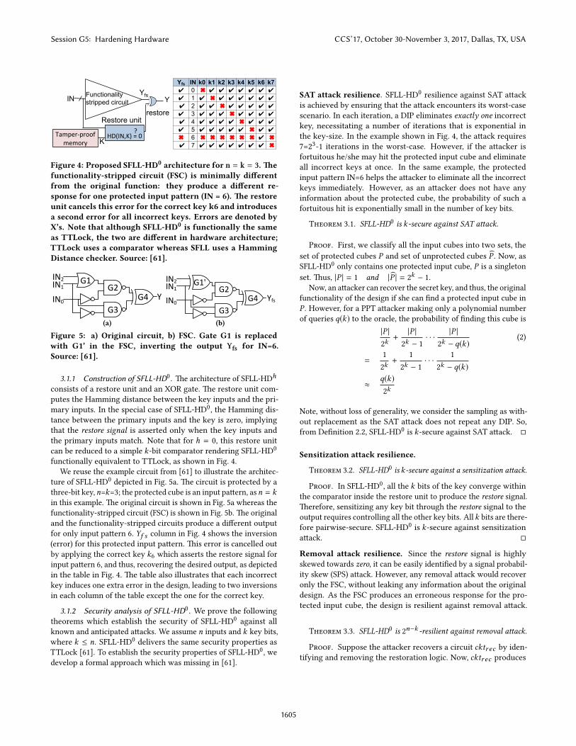
Functionality stripped circuit IN
K
Yfs
restore
Y
Restore unit
Tamper-proofmemory
Yfs IN k0 k1 k2 k3 k4 k5 k6 k7 ✔ 0 ✖ ✔ ✔ ✔ ✔ ✔ ✔ ✔ ✔ 1 ✔ ✖ ✔ ✔ ✔ ✔ ✔ ✔ ✔ 2 ✔ ✔ ✖ ✔ ✔ ✔ ✔ ✔ ✔ 3 ✔ ✔ ✔ ✖ ✔ ✔ ✔ ✔ ✔ 4 ✔ ✔ ✔ ✔ ✖ ✔ ✔ ✔ ✔ 5 ✔ ✔ ✔ ✔ ✔ ✖ ✔ ✔ ✖ 6 ✖ ✖ ✖ ✖ ✖ ✖ ✔ ✖ ✔ 7 ✔ ✔ ✔ ✔ ✔ ✔ ✔ ✖
?
HD(IN,K)=0
Figure 4: Proposed SFLL-HD0 architecture for n = k = 3. �efunctionality-stripped circuit (FSC) is minimally di�erentfrom the original function: they produce a di�erent re-sponse for one protected input pattern (IN = 6). �e restoreunit cancels this error for the correct key k6 and introducesa second error for all incorrect keys. Errors are denoted byX’s. Note that although SFLL-HD0 is functionally the sameas TTLock, the two are di�erent in hardware architecture;TTLock uses a comparator whereas SFLL uses a HammingDistance checker. Source: [61].
G2IN2
YIN1
IN0G3
G4
G1
(a)
G2IN2
YfsIN1
IN0G3
G1'
G4
(b)
Figure 5: a) Original circuit, b) FSC. Gate G1 is replacedwith G1’ in the FSC, inverting the output Yfs for IN=6.Source: [61].
3.1.1 Construction of SFLL-HD0. �e architecture of SFLL-HDh
consists of a restore unit and an XOR gate. �e restore unit com-
putes the Hamming distance between the key inputs and the pri-
mary inputs. In the special case of SFLL-HD0, the Hamming dis-
tance between the primary inputs and the key is zero, implying
that the restore signal is asserted only when the key inputs and
the primary inputs match. Note that for h = 0, this restore unit
can be reduced to a simple k-bit comparator rendering SFLL-HD0
functionally equivalent to TTLock, as shown in Fig. 4.
We reuse the example circuit from [61] to illustrate the architec-
ture of SFLL-HD0
depicted in Fig. 5a. �e circuit is protected by a
three-bit key, n=k=3; the protected cube is an input pa�ern, asn = kin this example. �e original circuit is shown in Fig. 5a whereas the
functionality-stripped circuit (FSC) is shown in Fig. 5b. �e original
and the functionality-stripped circuits produce a di�erent output
for only input pa�ern 6. Yf s column in Fig. 4 shows the inversion
(error) for this protected input pa�ern. �is error is cancelled out
by applying the correct key k6 which asserts the restore signal for
input pa�ern 6, and thus, recovering the desired output, as depicted
in the table in Fig. 4. �e table also illustrates that each incorrect
key induces one extra error in the design, leading to two inversions
in each column of the table except the one for the correct key.
3.1.2 Security analysis of SFLL-HD0. We prove the following
theorems which establish the security of SFLL-HD0
against all
known and anticipated a�acks. We assume n inputs and k key bits,
where k ≤ n. SFLL-HD0
delivers the same security properties as
TTLock [61]. To establish the security properties of SFLL-HD0, we
develop a formal approach which was missing in [61].
SAT attack resilience. SFLL-HD0
resilience against SAT a�ack
is achieved by ensuring that the a�ack encounters its worst-case
scenario. In each iteration, a DIP eliminates exactly one incorrect
key, necessitating a number of iterations that is exponential in
the key-size. In the example shown in Fig. 4, the a�ack requires
7=23-1 iterations in the worst-case. However, if the a�acker is
fortuitous he/she may hit the protected input cube and eliminate
all incorrect keys at once. In the same example, the protected
input pa�ern IN=6 helps the a�acker to eliminate all the incorrect
keys immediately. However, as an a�acker does not have any
information about the protected cube, the probability of such a
fortuitous hit is exponentially small in the number of key bits.
Theorem 3.1. SFLL-HD0 is k-secure against SAT a�ack.
Proof. First, we classify all the input cubes into two sets, the
set of protected cubes P and set of unprotected cubes P . Now, as
SFLL-HD0
only contains one protected input cube, P is a singleton
set. �us, |P | = 1 and |P | = 2k − 1.
Now, an a�acker can recover the secret key, and thus, the original
functionality of the design if she can �nd a protected input cube in
P . However, for a PPT a�acker making only a polynomial number
of queries q(k) to the oracle, the probability of �nding this cube is
|P |2k+|P |
2k − 1
· · · |P |2k − q(k)
(2)
=1
2k+
1
2k − 1
· · · 1
2k − q(k)
≈ q(k)2k
Note, without loss of generality, we consider the sampling as with-
out replacement as the SAT a�ack does not repeat any DIP. So,
from De�nition 2.2, SFLL-HD0
is k-secure against SAT a�ack. �
Sensitization attack resilience.
Theorem 3.2. SFLL-HD0 is k-secure against a sensitization a�ack.
Proof. In SFLL-HD0, all the k bits of the key converge within
the comparator inside the restore unit to produce the restore signal.
�erefore, sensitizing any key bit through the restore signal to the
output requires controlling all the other key bits. All k bits are there-
fore pairwise-secure. SFLL-HD0
is k-secure against sensitization
a�ack. �
Removal attack resilience. Since the restore signal is highly
skewed towards zero, it can be easily identi�ed by a signal probabil-
ity skew (SPS) a�ack. However, any removal a�ack would recover
only the FSC, without leaking any information about the original
design. As the FSC produces an erroneous response for the pro-
tected input cube, the design is resilient against removal a�ack.
Theorem 3.3. SFLL-HD0 is 2n−k -resilient against removal a�ack.
Proof. Suppose the a�acker recovers a circuit cktr ec by iden-
tifying and removing the restoration logic. Now, cktr ec produces
Session G5: Hardening Hardware CCS’17, October 30-November 3, 2017, Dallas, TX, USA
1605

an incorrect output for the set of protected input cubes, denoted as
P . However, we know that each cube contains 2n−k
input pa�erns.
�us, if Γ denotes the set of all input pa�erns contained in P ,
cktr ec (i) , F (i), ∀i ∈ Γ|Γ | = |P | × 2
n−k(3)
= 1 × 2n−k
= 2n−k
So, from De�nition 2.4, SFLL-HD0
is 2n−k
-resilient against a re-
moval a�ack. �
3.2 SFLL-HDh
In this section, we generalize for h; SFLL-HDh can protect all input
cubes that are of Hamming distance of h from the secret key. �e
number of protected input cubes is
(kh).
3.2.1 Construction of SFLL-HDh . With a HD of h, an input-size
of n, and key-size of k , SFLL-HDh
inverts the FSC output Yf s for(kh)
input cubes, which contains 2n−k ·
(kh)
pa�erns. �e restore
unit, which comprises of k XOR gates and an adder to compute
the Hamming distance, recti�es all these errors for the correct
key, while it introduces a di�erent but possibly overlapping set of
errors for any incorrect key. Fig. 6 depicts the architecture of the
proposed SFLL-HDh
along with an example where n = k = 3 and
h = 1. As can be seen from the architecture, the implementation
overhead of the restore unit is independent of h, which is a hard-
coded (non-secret) constant that feeds the comparator inside the
restore unit.
3.2.2 Security analysis of SFLL-HDh . We assume n inputs and kkey bits, k ≤ n. Proofs of theorems are provided in Appendix B.1.
SAT attack resilience.
Theorem 3.4. SFLL-HDh is (k − dlog2
(kh)e)-secure against SAT
a�ack.
Sensitization attack resilience.
Theorem 3.5. SFLL-HDh is k-secure against sensitization a�ack.
Functionality stripped circuit IN
?
HD(IN,K) = h K
Yfs
restore
Y
Restore unit
Tamper-‐proof Memory
Yfs IN k0 k1 k2 k3 k4 k5 k6 k7 ✔ 0 ✖ ✖ ✖ ✔ ✖ ✔ ✔ ✔ ✔ 1 ✔ ✔ ✔ ✖ ✔ ✖ ✔ ✔ ✖ 2 ✔ ✖ ✖ ✔ ✖ ✖ ✔ ✖ ✔ 3 ✔ ✖ ✖ ✔ ✔ ✔ ✔ ✖ ✖ 4 ✔ ✖ ✖ ✖ ✖ ✔ ✔ ✖ ✔ 5 ✔ ✖ ✔ ✔ ✖ ✔ ✔ ✖ ✔ 6 ✔ ✔ ✖ ✔ ✖ ✔ ✔ ✖ ✖ 7 ✖ ✖ ✖ ✔ ✖ ✔ ✔ ✖
Figure 6: SFLL-HDh architecture for n=k=3 and h=1. Yfs in-cludes
(kh)errors, denoted by X’s. Restore unit recti�es all
errors for the correct key k6. For the incorrect keys, restoreunit introduces
(kh)additional errors (at
(kh)input patterns),
which may possibly coincide and cancel errors in Yfs.
Removal attack resilience.
Theorem 3.6. SFLL-HDh is 2n−k ·
(kh)-resilient against removal
a�ack.
As these theorems show, h can be adjusted to trade resilience
to one a�ack for resilience to another. Values of h closer to either
0 or k deliver higher resilience to SAT and other key-pruning at-
tacks, whereas resilience to the removal a�ack can be maximized
by se�ing h=k/2.
4 SFLL-FLEXIn contrast to SFLL-HD
h, SFLL-�ex
c×kallows the user to specify,
and thus, protect the IP-critical input pa�erns; the restore unit
stores the protected input pa�erns in a compact form, i.e., in the
form of c input cubes, each with k speci�ed bits. In this context, the
input cubes can be conceived as the secret keys to be loaded onto
the chip for the restore unit to recover the stripped functionality.
We will use the terms “protected input cubes” and “secret keys”
interchangeably for SFLL-�exc×k
. �e SFLL-�exc×k
framework
is shown in Fig. 7; in this section, we elaborate on the individual
processes in this framework.
In a design with multiple outputs, not every output needs pro-
tection; only the IP-critical part of the design has to be protected to
control the cost of logic locking, which is at the discretion of the
designer. SFLL-�exc×k
enables the outputs to be selectively �ipped
(and restored) for the protected input cubes; a �ip vector associated
with each protected input cube holds information regarding which
outputs are to be �ipped for the protected input cube.
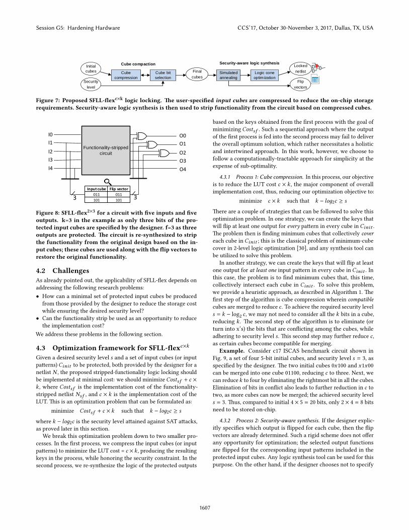
Example. Fig. 8 presents an overview of SFLL-�exc×k
. �e FSC
di�ers from the original circuit for two protected input cubes x01x1
and x10x1, collectively representing 8 input pa�erns. �e restore
unit stores the two input cubes and the corresponding �ip vectors.
In this example, only three out of �ve outputs are protected.
4.1 Architecture�e restore unit of SFLL-�ex
c×kconsists of a tamper-proof [50]
look-up table (LUT) and XOR gates. �e LUT stores c k-bit input
cubes along with the corresponding f -bit �ip vectors (for protecting
f out of m outputs) that dictate the functionality stripped from
the circuit.2
When the input matches an entry in the LUT, the
associated �ip vector is retrieved from the table and XORed with
the outputs to restore the original functionality.
Cost. �e cost of SFLL-�exc×k
is proportional to the size of
the LUT, in addition to f XOR gates inserted at the outputs of
the FSC. �e cost of the LUT is denoted as c × (k + f ), where fis a designer-de�ned parameter. Cost minimization requires the
minimization of c and k . Additionally, functionality stripping can
be used as an opportunity to reduce implementation cost as will be
discussed in Section 4.3. �us, the net cost of SFLL-�exc×k
is this
saving subtracted from the LUT cost.
2One extreme case of SFLL-�ex
c×kis to strip the entire functionality of the design;
such an approach would incur a prohibitive overhead, as the entire truth table, whose
size is exponential in the number of inputs, needs to be stored on-chip.
Session G5: Hardening Hardware CCS’17, October 30-November 3, 2017, Dallas, TX, USA
1606
Simulated
annealing
Security-aware logic synthesis
Logic cone
optimization
Cube
compression
Cube bit
selection
Initial
cubes
Security
level
Final
cubes
Cube compaction Locked
netlist
Flip
vectors
Figure 7: Proposed SFLL-�exc×k logic locking. �e user-speci�ed input cubes are compressed to reduce the on-chip storagerequirements. Security-aware logic synthesis is then used to strip functionality from the circuit based on compressed cubes.
Functionality-stripped
circuit
I0
I1
I2
I3
I4
O0
O1
O2
O3
O4
Input cube
011
101
Flip vector
011
1013 3
Figure 8: SFLL-�ex2×3 for a circuit with �ve inputs and �veoutputs. k=3 in the example as only three bits of the pro-tected input cubes are speci�ed by the designer. f=3 as threeoutputs are protected. �e circuit is re-synthesized to stripthe functionality from the original design based on the in-put cubes; these cubes are used along with the �ip vectors torestore the original functionality.
4.2 ChallengesAs already pointed out, the applicability of SFLL-�ex depends on
addressing the following research problems:
• How can a minimal set of protected input cubes be produced
from those provided by the designer to reduce the storage cost
while ensuring the desired security level?
• Can the functionality strip be used as an opportunity to reduce
the implementation cost?
We address these problems in the following section.
4.3 Optimization framework for SFLL-�exc×kGiven a desired security level s and a set of input cubes (or input
pa�erns) Cinit to be protected, both provided by the designer for a
netlist N , the proposed stripped-functionality logic locking should
be implemented at minimal cost: we should minimize Costsf + c ×k , where Costsf is the implementation cost of the functionality-
stripped netlist Nsf , and c × k is the implementation cost of the
LUT. �is is an optimization problem that can be formulated as:
minimize Costsf + c × k such that k − loд2c ≥ s
where k − loд2c is the security level a�ained against SAT a�acks,
as proved later in this section.
We break this optimization problem down to two smaller pro-
cesses. In the �rst process, we compress the input cubes (or input
pa�erns) to minimize the LUT cost = c × k , producing the resulting
keys in the process, while honoring the security constraint. In the
second process, we re-synthesize the logic of the protected outputs
based on the keys obtained from the �rst process with the goal of
minimizing Costsf . Such a sequential approach where the output
of the �rst process is fed into the second process may fail to deliver
the overall optimum solution, which rather necessitates a holistic
and intertwined approach. In this work, however, we choose to
follow a computationally-tractable approach for simplicity at the
expense of sub-optimality.
4.3.1 Process 1: Cube compression. In this process, our objective
is to reduce the LUT cost c × k , the major component of overall
implementation cost, thus, reducing our optimization objective to:
minimize c × k such that k − loд2c ≥ s
�ere are a couple of strategies that can be followed to solve this
optimization problem. In one strategy, we can create the keys that
will �ip at least one output for every pa�ern in every cube in Cinit .
�e problem then is �nding minimum cubes that collectively covereach cube in Cinit ; this is the classical problem of minimum-cube
cover in 2-level logic optimization [30], and any synthesis tool can
be utilized to solve this problem.
In another strategy, we can create the keys that will �ip at least
one output for at least one input pa�ern in every cube in Cinit . In
this case, the problem is to �nd minimum cubes that, this time,
collectively intersect each cube in Cinit . To solve this problem,
we provide a heuristic approach, as described in Algorithm 1. �e
�rst step of the algorithm is cube compression wherein compatiblecubes are merged to reduce c . To achieve the required security level
s = k − log2c , we may not need to consider all the k bits in a cube,
reducing k . �e second step of the algorithm is to eliminate (or
turn into x’s) the bits that are con�icting among the cubes, while
adhering to security level s . �is second step may further reduce c ,
as certain cubes become compatible for merging.
Example. Consider c17 ISCAS benchmark circuit shown in
Fig. 9, a set of four 5-bit initial cubes, and security level s = 3, as
speci�ed by the designer. �e two initial cubes 0x100 and x1x00
can be merged into one cube 01100, reducing c to three. Next, we
can reduce k to four by eliminating the rightmost bit in all the cubes.
Elimination of bits in con�ict also leads to further reduction in c to
two, as more cubes can now be merged; the achieved security level
s = 3. �us, compared to initial 4 × 5 = 20 bits, only 2 × 4 = 8 bits
need to be stored on-chip.
4.3.2 Process 2: Security-aware synthesis. If the designer explic-
itly speci�es which output is �ipped for each cube, then the �ip
vectors are already determined. Such a rigid scheme does not o�er
any opportunity for optimization; the selected output functions
are �ipped for the corresponding input pa�erns included in the
protected input cubes. Any logic synthesis tool can be used for this
purpose. On the other hand, if the designer chooses not to specify
Session G5: Hardening Hardware CCS’17, October 30-November 3, 2017, Dallas, TX, USA
1607
O2G6
Initial cubes Final cubes
0x100
x1x00
01101
0111x
I1I2
I3
I4
I5
O1G1
G2
G5
G4
O2G6
I1I2I3
I4
I5
O1G1
G2
G5
G4
O2G6
Cube
01100111
FlipVector
0010
4
G7
01100
01101
0111x
0110
0111
Compressed cubes
(b) (c) (d)
I1I2
I3
I4
I5
O1G1
G2
G3
G5
G4
(a)
Figure 9: Application of SFLL-�ex to c17 ISCAS circuit. a) Original circuit. b) Cube compression. c) FSC. d) Locked circuit.
Algorithm 1: Cube compression algorithm
Input : Initial cubes Cinit , Security level sOutput :Final cubes C
1 C ← merge compatible cubes(Cinit )
2 snew ← k − log2c
3 while snew ≥ s do4 C ← eliminate con�icting bit(C)
5 C ← merge compatible cubes(C)
6 snew ← update security level(c,k)
7 end
Algorithm 2: Security-aware synthesis algorithm
Input :Original netlist N , Final cubes COutput :Functionality-stripped netlist Nsf , Flip vector V
1 V ← init �ip vector(N )2 Nsf ←rand soln(N ,C)3 costsf ← cost(Nsf )4 T = 1.0,Tmin = 0.00001,α = 0.9
5 while T > Tmin do6 for i = 1 to 200 do7 Nnew ←neighbor(Nsf ,C)8 costnew ← cost(Nnew )
9 if Rand(0, 1) < exp( costnew−costsfT ) then10 Nsf ← Nnew
11 costsf ← costnew12 V ← update �ip vector(Nsf ,po)13 end14 end15 T = T × α16 end
the �ip vectors, a security-aware synthesis process can leverage
this �exibility to minimize implementation cost of the functionality-
stripped design Nsf without compromising security. �e process
also produces the �ip vectors, denoted by V , as described in Algo-
rithm 2.
Algorithm 2 starts with the original netlist N and a set of cubes
C . Initially, a random solution Nsf with the associated cost costsfis generated by initializing the �ip vector V with a random value.
From this random solution, simulated annealing starts optimization
by selecting a neighboring solution at each iteration. A new solution
Nnew is generated by changing a random bit in the �ip vector V ,
which leads to inclusion/exclusion of the corresponding cube for
a particular output. �e solution Nnew is accepted if it yields cost
savings, i.e. costnew < costsf . An inferior solution may be accepted
with a probability of exp( costopt−costnewT ). �is is a key feature of
simulated annealing for exploring a larger search space without
ge�ing stuck at a local optimum.
Example. Let us consider the application of security-aware
synthesis to the c17 circuit in Fig. 9. Algorithm 2 operates on the
original c17 netlist and the �nal cubes produced by Algorithm 1,
and produces the FSC; AND gate G3 is removed from the logic cone
O1. �e �ip vector 10 will restore the stripped functionality for
logic cone O1 by �ipping its output for the cube 0110x.
4.4 Security analysis for SFLL-�exc×k
In this section, we discuss the resilience of SFLL-�exc×k
against the
state-of-the-art a�acks. �e proofs of theorems below are provided
in Appendix B.2.
SAT attack resilience. An a�acker, following a SAT-based or a
random guess a�ack model, must identify all input pa�erns of the
protected input cubes in SFLL-�exc×k
to be able to recover the
correct functionality of the original design from the on-chip imple-
mentation; in contrast to SFLL-HDh
, the protected input cubes can
be arbitrary in SFLL-�exc×k
, and one cube does not infer another.
�is requires the retrieval of the content of the entire LUT that
represents the stripped functionality. Nevertheless, we assess the
security strength of SFLL conservatively; a�ack success is de�ned
by the a�acker’s ability to retrieve any input pa�ern that belongs to
one of the protected input cubes. �e following theorem establishes
the resilience of SFLL-�exc×k
against SAT a�ack.
Theorem 4.1. SFLL-�exc×k is (k − dlog2ce)-secure against SAT
a�ack.
Sensitization attack resilience.
Theorem 4.2. SFLL-�exc×k is k-secure against sensitization at-tack.
Removal attack resilience.
Theorem 4.3. SFLL-�exc×k is c · 2n−k -resilient against removala�ack.
As these theorems show, the number and the size of the protected
input cubes, denoted by c and k respectively, dictate the trade-o�
between resilience to oracle-guided and removal a�acks.
Session G5: Hardening Hardware CCS’17, October 30-November 3, 2017, Dallas, TX, USA
1608

29
211
213
215
# D
IPs
h=0
28
210
212
214h=1
24
26
28
210
212
214h=2
11 12 13 14
Key size (k)
0.0
0.4
0.8
1.2
1.6
Exec.
tim
e (
s)
1e4
11 12 13 14
Key size (k)
0.0
0.4
0.8
1.2
1.61e4
11 12 13 14
Key size (k)
0.0
0.4
0.8
1.2
1.61e4
s35932 s38417 s38584 b14 b15 b17 b18 b20 b21 b22
Figure 10: Results for SFLL-HDh for h={0,1,2}, and k={11,12,13,14}; the number of DIPs required for the SAT attack [44], andthe corresponding execution time in seconds.
5 SIMULATION RESULTS5.1 Experimental setupIn this section, we present the experimental results to validate the
security expectations and demonstrate the e�ectiveness of the pro-
posed SFLL techniques. �e experiments are executed on a 28-core
Intel Xeon processors running at 2GHz with 128 GB of RAM. We
lock the combinational part of the sequential benchmark circuits
from the ISCAS’89 [7] and ITC’99 [11] suites in our experiments.
Table 3 shows the statistics for the circuits; the largest circuit b18
has >100K gates. �e area, power, and delay (APD) overhead for
SFLL-HD and SFLL-�ex versions are obtained using Synopsys De-
sign Compiler along with Global Foundries 65nm LPe library. We
present the results of security analysis wherein di�erent variants
of the SAT a�ack are launched on various versions of SFLL-HD
and SFLL-�ex. In particular, we launch the SAT a�ack [44] and the
AppSAT [40] against the proposed techniques. Each a�ack experi-
ment is repeated ten times to improve the statistical signi�cance;
average results of the ten runs are reported.
5.2 SFLL-HDh
5.2.1 Security analysis. �e resilience of SFLL-HDh
is dictated
by the key-size k and h, which together dictate the number of
protected input cubes
(kh). In SFLL-HD experiments, we protect
the largest logic cone in each circuit. �e number of DIPs re-
quired for the SAT a�ack to succeed on SFLL-HDh
circuits, and
Table 3: Statistics for the largest ITC’99 [11] and IS-CAS’89 [7] benchmarks. LLC denotes the largest logic cone.
Benchmark Functionality Inputs Outputs Gate count LLC inputs
Small
s35932 N/A 1763 2048 12,204 195
s38417 N/A 1664 1742 8709 99
s38584 N/A 1464 1731 11448 147
b14 Viper processor 277 299 9,767 218
b15 80386 processor 485 519 8,367 306
Large
b17 3× b15 1452 1512 30,777 308
b18 2× b14 + 2× b17 3357 3343 111,241 271
b20 2× modi�ed b14 522 512 19,682 282
b21 2× b14 522 512 20,027 282
b22 3× modi�ed b14 767 757 29,162 283
the corresponding execution time are presented in Fig. 10 for
k={11, 12, 13, 14} and h={0, 1, 2}. Although the actual security lev-
els required in a practical se�ing are much larger (e.g., 64-bit or
128-bit), we cannot empirically assess the security of SFLL for such
high values due to computational limitations. For the sake of un-
derstanding the trends, we experiment with these small key-sizes.
Impact of key size k. Fig. 10 demonstrates that the number of
DIPs required for the SAT a�ack to succeed grows exponentially
in k , con�rming our theoretical expectation. For instance, the
expected number of DIPs required to break SFLL-HD0
is 2k−1
. �e
same trend holds for SFLL-HD1
and SFLL-HD2
as well, except for
a few cases, where an a�acker may be fortuitous and the a�ack
terminates earlier, reducing the average number of DIPs.
�e execution time of the SAT a�ack is proportional to the num-
ber of DIPs, although there is a slight variation of 3× to 4× across
the benchmark circuits; the execution time grows exponentially in
k .
Impact of Hamming distance h. SFLL-HDh
is (k−dlog2
(kh)e)-
secure. �us, an increase in h leads to a signi�cant change in the
security level and the expected number of DIPs required for the
SAT a�ack. For example, the average number of DIPs for the circuit
s38584 for h={0, 1, 2} and k=14 is 15K, 10K, and 5K, respectively, as
shown in Fig. 10.
5.2.2 APD overhead. �e APD overhead is obtained using Syn-
opsys DC Compiler using Global Foundries 65nm LPe library [43]
and is shown in Fig. 11 for k=128. �e overhead for SFLL-HD can
be a�ributed to two sources: the restore unit and the functionality-
stripped circuit. SFLL-HDh
restore unit comprises a single k-bit
comparator along with an adder unit, where the overhead is antici-
pated to increase linearly in k but to remain constant for h, which
is a hard-coded constant (as it need not be a secret). �e 128-bit
comparator and adder blocks incur a signi�cant area, power, and
delay overhead on small-sized circuits; for the smallest �ve bench-
marks (˜10K gates), area, power, and delay overhead are 28%, 50%,
-2%, respectively. For larger-sized circuits, however, the overhead
of the restore unit is amortized; for the largest �ve benchmarks, the
Session G5: Hardening Hardware CCS’17, October 30-November 3, 2017, Dallas, TX, USA
1609

0
50
100
Are
a (
%)
0
50
100
Pow
er
(%)
s35932s38417
s38584 b14 b15 b17 b18 b20 b21 b2220
10
0
10
Dela
y (
%)
h=0
h=4
h=8
h=12
Figure 11: Area, power, and delay overhead for SFLL-HDh
for k=128 and h={0,4,8,12}. �e APD overhead for the larger�ve benchmarks are 10%, 6%, and -5%, respectively; for thesmaller �ve benchmarks, they are 28%, 50%, and -2%, respec-tively.
s35932s38417
s38584 b14 b15 b17 b18 b20 b21 b220.0
0.5
1.0
Exec.
tim
e (
s)
1e3
h=0h=4
h=8h=12
Figure 12: Execution time of SFLL-HDh for k=128.
average area, power and delay overhead are only 10%, 6%, and -5%,
respectively, boding well for even larger-sized industrial circuits.
5.2.3 Scalability. SFLL-HDh
algorithm operates on the RT-level
circuit. Fig. 12 shows that the execution time of the SFLL-HD
algorithm is only a few minutes, irrespective of h. For b18 circuit
with more than 100K gates, the execution time is only about 15
minutes, con�rming the scalability of the proposed SFLL-HDh
.
5.3 SFLL-�exc×k5.3.1 Security analysis. To validate the security of SFLL-�ex,
we launch the SAT a�ack [44] and AppSAT [40] a�ack on circuits
locked using SFLL-�ex for c = {1, 2, 3} and k = {11, 12, 13, 14}.�e results shown in Fig. 13 demonstrate that the number of DIPs
for SFLL-�ex is exponential in k . With increasing c , we observe
a logarithmic decrease in the number of DIPs, in line with our
theoretical expectation. �e trends for the execution time is similar
to that for DIPs, except that the increase in execution time is more
prominent. While the DIPs double for each increment in k , the
execution time may increase by 3-5×. �e AppSAT [40] a�ack on
SFLL-�ex again fails in 100% of the cases.
5.3.2 Cube compression. �e savings for the cube compression
technique are presented in Table 4. In our experiments, we gener-
ate test cubes for randomly selected cinit stuck-at faults by using
Atalanta test pa�ern generation tool [25], and treat these test cubes
Table 4: Cube compression ratio R for SFLL-�exc×k.
Bench s=64 s=128
c = 32 c = 64 c = 32 c = 64
s35932 867.9 1735.9 437.3 874.7
s38417 403.4 806.8 136.5 409.6
s38584 354.9 1441.5 180.2 360.4
b14 26.5 52.9 6.7 14.9
b15 238.8 115.8 120.3 79.6
b17 352.0 469.3 59.1 70.4
b18 813.8 3305.4 832.7 234.3
b20 126.5 61.4 31.9 42.5
b21 49.9 99.7 31.9 36.4
b22 91.6 183.2 62.9 74.9
Average 332.5 827.2 190.0 219.8
as the designer-provided input cubes Cinit . �e compression ratio
R is computed as the ratio of the initial number of key bits to be
stored cinit × kinit to that of compressed key bits cf inal × kf inal ;kinit equals the number of inputs n. �e results are presented for
two di�erent security levels s = 64 and 128 and for two di�erent
numbers of initial cubes c = 32 and 64. On average, a compression
level of 400× is achieved, while still maintaining the desired secu-
rity level. �ese compression levels directly translate to a reduction
in implementation cost for the restore unit. It can be noted that a
lower security level (s = 64) enables a higher compression level.
5.3.3 Security-aware synthesis. We report the area, power, and
delay (APD) overhead separately for 1) the “optimal-cost” FSC (with-
out the restore unit) and 2) the overall circuit (with the restore unit
comprising the LUT and the surrounding combinational logic). �e
APD overhead is shown in Fig. 14a and Fig. 14b for target security
levels s = 64 bits and 128, respectively. �e simulated-annealing
based optimization is accomplished using area as the primary cost
metric. �e ABC [6] synthesis tool is used to convert a design to
And-Invert-Graph and the gate count is taken as the cost metric. It
can be inferred that security-aware synthesis incurs only a minimal
overall overhead of 5%, 4% and 2% for area, power, and delay for a
security level s = 64, and 11%, 8% and -1% for a security level s =128. In these �gures, negative values denote a reduction in APD
when compared to the original circuit due to the functionality-strip
operation; e.g., this can be seen for the circuit s35932 in its area
footprint. However, due to the overhead of the restore unit compris-
ing mostly sequential elements, the overall overhead is positive. In
majority of the cases, the delay overhead is almost negligible (˜0%).
�is is due to the fact that adding the restore unit does not actually
a�ect the delay of the critical path, thus, incurring no signi�cant
performance penalty.
�e combined execution time for cube compression and security-
aware synthesis is presented in Fig. 15. �e execution time for cube
compression is in the order of a few seconds. �e execution time for
security-aware synthesis is directly determined by the simulated
annealing parameters (the temperature T and the gradient α ) and
the size (number of gates) of a circuit. As can be seen from the �gure,
even for large circuits such as b18 with >100K gates, the synthesis
is completed in about two hours. Our empirical results indicate
that the execution time remains independent of the security level s
Session G5: Hardening Hardware CCS’17, October 30-November 3, 2017, Dallas, TX, USA
1610

27
29
211
213
215
# D
IPs
c=1
27
29
211
213
215c=2
26
28
210
212
214c=3
11 12 13 14k
0.0
0.4
0.8
1.2
Exec.
tim
e (
s)
1e3
11 12 13 14k
0.0
0.4
0.8
1.2
1e3
11 12 13 14k
0.0
0.4
0.8
1.2
1.61e3
s35932 s38417 s38584 b14 b15 b17 b18 b20 b21 b22
Figure 13: Results for SFLL-�exc×k for c={1,2,3} and k={11,12,13,14}; the number of DIPs required for the SAT attack [44] andthe corresponding execution time (seconds).
10
0
10
20
Are
a (
%)
5
0
5
10
Pow
er
(%)
s35932s38417
s38584 b14 b15 b17 b18 b20 b21 b2210
0
10
20
30
Dela
y (
%)
fs(c=32)
fs(c=64)
overall(c=32)
overall(c=64)
(a)
20
0
20
40
Are
a (
%)
10
0
10
20
30
Pow
er
(%)
s35932s38417
s38584 b14 b15 b17 b18 b20 b21 b2210
5
0
5
10
Dela
y (
%)
fs(c=32)
fs(c=64)
overall(c=32)
overall(c=64)
(b)Figure 14: Area, power, and delay overhead for SFLL-�exc×kfor number of initial cubes c=32 and c=64 and for securitylevel (a) s=64 and (b) s=128. �e overhead of the functional-ity stripped circuit, denoted as fs, is shown with dark shadeand overhead of the overall circuit including restore unit isshownwith light shade. �e average overhead for the largest�ve benchmarks are 6%, 4%, and -1.5% for area, power, and de-lay, respectively; for the smallest �ve benchmarks, the num-bers are 10%, 8%, and 1.5%, respectively.
s35932s38417
s38584 b14 b15 b17 b18 b20 b21 b220
2
4
6
8
Exec.
tim
e (
s)
1e3
k=64,c=32k=64,c=64
k=128,c=32k=128,c=64
Figure 15: Combined execution time of cube compressionand security-aware synthesis for SFLL-�exc×k.
and the number of protected cubes k , con�rming the scalability of
the proposed SFLL-�exc×k
.
5.4 Double-DIP/AppSAT attack resultsWhile the SAT a�ack terminates only upon retrieving the correct
key, the AppSAT [40] and Double-DIP [41] a�acks may (counter-intuitively) terminate earlier returning an incorrect key value, which
results in an approximate netlist [40]. �e termination criteria
for AppsAT is dictated by an error rate speci�ed by the a�acker,
whereas, Double-DIP terminates when it can no longer �nd DIPs
that eliminate at least two incorrect keys.
Double-DIP. Each of the 2-DIPs employed by the Double-DIP
a�ack can eliminate at least two incorrect keys. Since no such 2-
DIPs exist for SFLL-HD0
and SFLL-�ex1×k
, the a�ack will terminate
immediately, recovering an approximate netlist. For larger h and cvalues, each input pa�ern is a 2-DIP, leading to scalability issues
for the Double-DIP a�ack. As illustrated in Fig. 16, the a�ack then
behaves similarly to the SAT a�ack, except that the execution time
of the two a�acks may vary depending on the DIPs employed by
the two a�acks.
AppSAT. In our �rst set of AppSAT experiments, we used the
default AppSAT parameters as reported in [40], i.e., 50 random
queries to the oracle were employed at every 12th
iteration of
the a�ack. We observed that estimating the error rate using such
a small number of pa�erns can be misleading and result in pre-
mature termination of the AppSAT a�ack, even for circuit with
Session G5: Hardening Hardware CCS’17, October 30-November 3, 2017, Dallas, TX, USA
1611
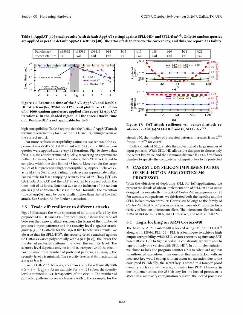
Table 5: AppSAT [40] attack results (with default AppSAT setting) against SFLL-HDh and SFLL-�exc×k. Only 50 randomqueriesare applied as per the default AppSAT settings [40]. �e attack fails to retrieve the correct key, and thus, we report it as failure.
Benchmark s35932 s38584 s38417 b14 b15 b17 b18 b20 b21 b22
Success/failure Fail Fail Fail Fail Fail Fail Fail Fail Fail Fail
0 1 2 3 4 5 6 7 8h
210
212
214
216
218
Exec.
tim
e (
sec) Timeout: 48 hours
Timeout for all attacks
Approx. netlist recovered by AppSAT
SAT
AppSAT
Double-DIP
Figure 16: Execution time of the SAT, AppSAT, and Double-DIP attack on (k=) 32-bit s38417 circuit plotted as a functionof h. 1000 randomqueries are applied a�er every 12AppSATiterations. In the shaded region, all the three attacks timeout. Double-DIP is not applicable for h=0.
high corruptibility. Table 5 reports that the “default” AppSAT a�ack
terminates erroneously for all of the SFLL circuits, failing to retrieve
the correct netlist.
For more realistic corruptibility estimates, we repeated the ex-
periments on s38417 SFLL-HD circuit with 32 key bits. 1000 random
queries were applied a�er every 12 iterations. Fig. 16 shows that
for h ≤ 3, the a�ack terminated quickly, recovering an approximate
netlist. However, for the same h values, the SAT a�ack failed to
complete within the time limit of 48 hours. Moreover, for the larger
values of h, representing higher corruptibility, AppSAT behaves ex-
actly like the SAT a�ack, failing to retrieve an approximate netlist.
For example, forh = 4 (implying security level of 32−dlog2
(32
4
)e=15
bits), both AppSAT and the SAT a�ack fail to succeed within the
time limit of 48 hours. Note that due to the inclusion of the random
queries (and additional clauses in the SAT formula), the execution
time of AppSAT may be occasionally higher than that of the SAT
a�ack. See Section 7.3 for further discussion.
5.5 Trade-o�: resilience to di�erent attacksFig. 17 illustrates the wide spectrum of solutions o�ered by the
proposed SFLL-HD and SFLL-�ex techniques; it shows the trade-o�
between the removal a�ack resilience (in terms of the number of
protected input pa�erns) and the security level s against oracle-
guide (e.g., SAT) a�acks for the largest �ve benchmark circuits. We
observe that for SFLL-HDh
, the security-level s a�ained against
SAT a�acks varies polynomially with h (h ∈ [0,k]); the larger the
number of protected pa�erns, the lower the security level. �e
security level depends only on k and h, irrespective of the circuit.
For the maximum number of protected pa�erns, i.e., h=n/2, the
security level s is minimal. �e security level is at its maximum at
h = 0 or h = k .
For SFLL-�exc×k
, however, s decreases only logarithmically with
c (s = k − dlog2ce). As an example, for c = 128 cubes, the security
level s a�ained is 121, irrespective of the circuit. �e number of
protected pa�erns increases linearly with c . For example, for the
0 32 64 96 128h
21384
23215
238423842629# p
rote
cted
pa
ttte
rns
b17b18
b20b21
b22
0
32
64
96
128
Secu
rity
leve
l s
(a)
0 32 64 96 128c
21384
23215
238423842629
# p
rote
cted
pa
ttte
rns
b17b18
b20b21
b22
0
32
64
96
128
Secu
rity
leve
l
(b)Figure 17: SAT attack resilience vs. removal attack re-silience; k=128. (a) SFLL-HDh and (b) SFLL-�exc×k.
circuit b20, the number of protected pa�erns increases from 2384
for c=1 to 2391
for c=128.
Both variants of SFLL enable the protection of a large number of
input pa�erns. While SFLL-HD allows the designer to choose only
the secret key value and the Hamming distance h, SFLL-�ex allows
him/her to specify the complete set of input cubes to be protected.
6 CASE STUDY: SILICON IMPLEMENTATIONOF SFLL-HD0 ON ARM CORTEX-M0PROCESSOR
With the objective of deploying SFLL for IoT applications, we
present the details of silicon implementation of SFLL on an in-housedesigned microcontroller using ARM Cortex-M0 microprocessor [2].
For accurate comparisons, we fabricated both the baseline and the
SFLL-locked microcontroller. Cortex-M0 belongs to the family of
Cortex-M 32-bit RISC processor series from ARM, suitable for a
variety of low-cost microcontrollers. �e microcontroller includes
ARM AHB-Lite as its BUS, UART interface, and 64 KB of SRAM.
6.1 Logic locking on ARM Cortex-M0�e baseline ARM Cortex-M0 is locked using 128-bit SFLL-HD
0
along with 128-bit FLL [36]. FLL is a technique to achieve high
output corruptibility, while SFLL ensures security against any SAT-
based a�ack. Due to tight scheduling constraints, we were able to
tape-out only one version with SFLL-HD0. In our implementation,
we chose to lock the program counter (PC) to safeguard against
unauthorized execution. �is ensures that an a�acker with an
incorrect key would end up with an incorrect execution due to the
corrupted PC. Ideally, the secret key is stored in a tamper-proof
memory, such as one-time programmable fuse ROM. However, in
our implementation, the 256-bit key for the locked processor is
stored in a write-only con�guration register. �e locked processor
Session G5: Hardening Hardware CCS’17, October 30-November 3, 2017, Dallas, TX, USA
1612
(a)(b)
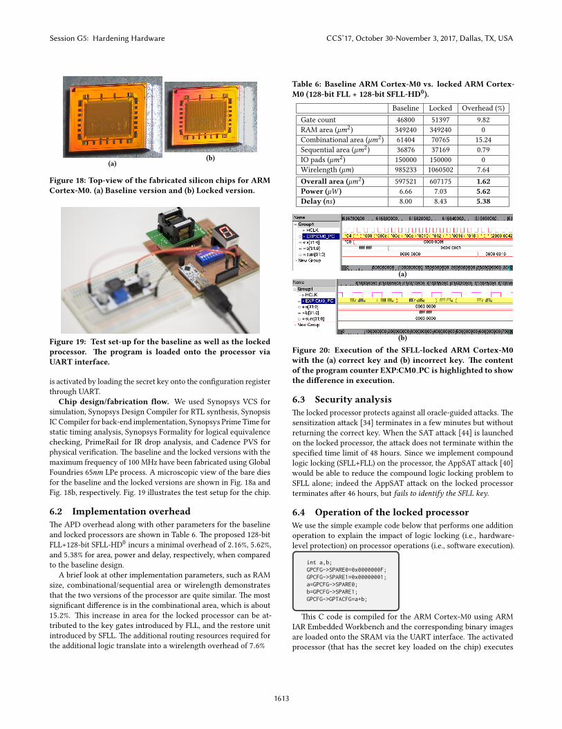
Figure 18: Top-view of the fabricated silicon chips for ARMCortex-M0. (a) Baseline version and (b) Locked version.
Figure 19: Test set-up for the baseline as well as the lockedprocessor. �e program is loaded onto the processor viaUART interface.
is activated by loading the secret key onto the con�guration register
through UART.
Chip design/fabrication �ow. We used Synopsys VCS for
simulation, Synopsys Design Compiler for RTL synthesis, Synopsis
IC Compiler for back-end implementation, Synopsys Prime Time for
static timing analysis, Synopsys Formality for logical equivalence
checking, PrimeRail for IR drop analysis, and Cadence PVS for
physical veri�cation. �e baseline and the locked versions with the
maximum frequency of 100 MHz have been fabricated using Global
Foundries 65nm LPe process. A microscopic view of the bare dies
for the baseline and the locked versions are shown in Fig. 18a and
Fig. 18b, respectively. Fig. 19 illustrates the test setup for the chip.
6.2 Implementation overhead�e APD overhead along with other parameters for the baseline
and locked processors are shown in Table 6. �e proposed 128-bit
FLL+128-bit SFLL-HD0
incurs a minimal overhead of 2.16%, 5.62%,
and 5.38% for area, power and delay, respectively, when compared
to the baseline design.
A brief look at other implementation parameters, such as RAM
size, combinational/sequential area or wirelength demonstrates
that the two versions of the processor are quite similar. �e most
signi�cant di�erence is in the combinational area, which is about
15.2%. �is increase in area for the locked processor can be at-
tributed to the key gates introduced by FLL, and the restore unit
introduced by SFLL. �e additional routing resources required for
the additional logic translate into a wirelength overhead of 7.6%
Table 6: Baseline ARM Cortex-M0 vs. locked ARM Cortex-M0 (128-bit FLL + 128-bit SFLL-HD0).
Baseline Locked Overhead (%)
Gate count 46800 51397 9.82
RAM area (µm2) 349240 349240 0
Combinational area (µm2) 61404 70765 15.24
Sequential area (µm2) 36876 37169 0.79
IO pads (µm2) 150000 150000 0
Wirelength (µm) 985233 1060502 7.64
Overall area (µm2) 597521 607175 1.62Power (µW ) 6.66 7.03 5.62Delay (ns) 8.00 8.43 5.38
(a)
(b)
Figure 20: Execution of the SFLL-locked ARM Cortex-M0with the (a) correct key and (b) incorrect key. �e contentof the program counter EXP:CM0 PC is highlighted to showthe di�erence in execution.
6.3 Security analysis�e locked processor protects against all oracle-guided a�acks. �e
sensitization a�ack [34] terminates in a few minutes but without
returning the correct key. When the SAT a�ack [44] is launched
on the locked processor, the a�ack does not terminate within the
speci�ed time limit of 48 hours. Since we implement compound
logic locking (SFLL+FLL) on the processor, the AppSAT a�ack [40]
would be able to reduce the compound logic locking problem to
SFLL alone; indeed the AppSAT a�ack on the locked processor
terminates a�er 46 hours, but fails to identify the SFLL key.
6.4 Operation of the locked processorWe use the simple example code below that performs one addition
operation to explain the impact of logic locking (i.e., hardware-
level protection) on processor operations (i.e., so�ware execution).
int a,b;GPCFG->SPARE0=0x0000000F;GPCFG->SPARE1=0x00000001;a=GPCFG->SPARE0;b=GPCFG->SPARE1;GPCFG->GPTACFG=a+b;
�is C code is compiled for the ARM Cortex-M0 using ARM
IAR Embedded Workbench and the corresponding binary images
are loaded onto the SRAM via the UART interface. �e activated
processor (that has the secret key loaded on the chip) executes
Session G5: Hardening Hardware CCS’17, October 30-November 3, 2017, Dallas, TX, USA
1613

the code correctly as shown in Fig. 20a; the addition of 0x01 and
0x0F produces 0x10 as expected. On the other hand, the locked
processor (with an incorrect key loaded) cannot execute the code
correctly, as shown in Fig. 20b, as the program counter is corrupted.
An exception handler is then called, rese�ing the PC to the default
value of 0xFFF7 FFFE, causing the execution to go into an in�nite
loop.
7 DISCUSSION7.1 Comparative security analysisTable 7 presents a comparison of SFLL-HD and SFLL-�ex with other
logic locking techniques. Existing SAT a�ack resilient techniques
such as SARLock and Anti-SAT are vulnerable to removal a�acks.
�e proposed SFLL thwarts all known a�acks on logic locking.
Further, it allows a designer to cost-e�ectively explore the trade-o�
between resilience to SAT and removal a�acks.
7.2 Choosing between SFLL-HD and SFLL-�exWhile SFLL-HD is suitable for generic applications where the main
requirement is to protect a large number of input pa�erns with min-
imal overhead, SFLL-�ex allows a designer to protect speci�c input
cubes. �e capability to specify IP-critical cubes to protect, even
a small number of them, may be very bene�cial for applications
such as microprocessors with IP-critical controllers, digital signal
processing applications with IP-critical coe�cients, etc. �e �exi-
bility required in SFLL-�ex necessitates a slightly more expensive
restore unit mainly due to the LUT, compared to SFLL-HD, which
has a generic, simple, and scalable restore unit. In either case, the
security-aware synthesis framework enables the designer to a�ain
the desired security level.
7.3 Resilience against the derivative attacksIn this section, we discuss the security of SFLL against the a�acks
that have been derived from the SAT a�ack, namely AppSAT [40],
Double-DIP [41], and Bypass [53]. �ese a�acks mainly target
compound (multi-layered) logic locking techniques. AppSAT and
Double-DIP are approximate a�acks as they only reduce a com-
pound logic locking technique (e.g. SARLock+SLL) to a SAT a�ack
resilient technique (e.g. SARLock). �e Bypass a�ack, however, is
an exact a�ack; the a�ack, if successful, returns a netlist function-
ally equivalent to the oracle (functional IC).
�ese a�acks rely on the classi�cation of compound logic locking
key bits into two classes: key bits for RLL/SLL etc. that introduce
high corruptibility and key bits for SARLock/Anti-SAT etc. that
induce low corruptibility at the outputs. �ese a�acks can quickly
determine the correct values for the high corruptibility key bits. �e
AppSAT and Double-DIP a�acks then assign a random value for the
low corruptibility key bits, whereas, the Bypass a�ack introduces
additional logic to �x the occasional corruption at the outputs.
�ese a�acks will not be e�ective against SFLL as all the key bits in
SFLL incur uniform corruptibility and it is not feasible to partition
the key search space into low/high corruptibility regions.
AppSAT. �ere are two main di�erences between AppSAT and
the SAT a�ack. First, AppSAT is constructed by augmenting the
SAT a�ack with random queries to the oracle at regular intervals.
As reported in [40], AppSAT involves 50 random queries every 12
iterations of the a�ack. Second, AppSAT can terminate much earlier
than the SAT a�ack, i.e., when the error rate (or Hamming distance
at the outputs) is below a certain threshold (e.g.,1
2k ). While the
AppSAT a�ack can quickly recover an approximate netlist for low-
corruptibility SFLL circuits (with low h or c ), it behaves similarly to
the SAT a�ack for high-corruptibility SFLL circuits since the early
termination condition is not satis�ed. �us, SFLL resilience against
AppSAT is similar to that against the SAT a�ack.
�e 50 queries as per the default AppSAT se�ings are su�cient
to separate the key bits into two classes in case of compound lock-
ing techniques. However, no such classes of key bits exist in SFLL
where the corruptibility is uniform for all the key values. As re-
ported in Section 5.2.1, when the a�ack is launched on SFLL circuits
with varying corruptibility values (represented using h), the a�ack
terminated erroneously even for high corruptibility circuits. �e
error is be�er estimated with 1000 random queries. �e a�ack then
quickly extracts the approximate netlist for the smaller values of h.
For the larger h values, the a�ack performance is similar to that of
the SAT a�ack.
Double-DIP. Compared to the SAT a�ack, the Double-DIP at-
tack uses a larger miter circuit comprising four copies of the locked
netlist [41]. �e 2-DIPs computed by the a�ack eliminate at least
two incorrect keys per DIP. �e a�ack terminates when no more
2-DIPs can be found, implying that only DIPs that can eliminate
at most one incorrect key remain in the search space. �e a�ack
returns an approximate netlist. While the a�ack can break com-
pound logic locking techniques, it is not scalable, especially if the
locked circuit has multiple correct keys.
Except for SFLL-HD0
or SFLL-Flex1×k
(whrere there are no 2-
DIPs), the Double-DIP a�ack, when launched on SFLL circuits, will
run into scalability issues as it will compute an exponential number
of DIPs before it terminates. Rarely, when the a�ack is fortuitous
and selects one of the protected pa�erns as a DIP (the protected
pa�ern may be a 2-DIP), it can eliminate most of the incorrect keys
in a single iteration of the a�ack. In such cases, the a�ack returns
returns the exact netlist, similar to the basic SAT a�ack, but this is
highly unlikely for large enough key sizes.
Bypass. �e Bypass a�ack selects two random key values as
constraints for the two locked netlists in the miter circuit [53]. �e
a�ack then computes all the DIPs that result in di�ering outputs for
the two key values. For the traditional low corruptibility locking
techniques such as SARLock, only a few DIPs will be extracted. �e
a�acker then determines the correct key values for those DIPs from
the output of functional IC. One of the two key values is designated
as the secret key and an additional bypass circuit is added around
the locked netlist to �x the output for the selected DIPs.
In SFLL, a protected input pa�ern produces the same incorrect
output for most of the incorrect key values. Occasionally, the
output may be correctly restored even for incorrect key values, as
illustrated earlier in Figure 4. When applied to SFLL, the Bypass
a�ack fails to compute the complete set of DIPs that lead to incorrect
outputs for the two key values. Most of the DIPs yield exactly the
same incorrect output for both incorrect keys, and as such, cannot
be extracted using the miter construction employed by the Bypass
a�ack. �e bypass circuitry, when constructed using an incomplete
set of DIPs, will be erroneous.
Session G5: Hardening Hardware CCS’17, October 30-November 3, 2017, Dallas, TX, USA
1614
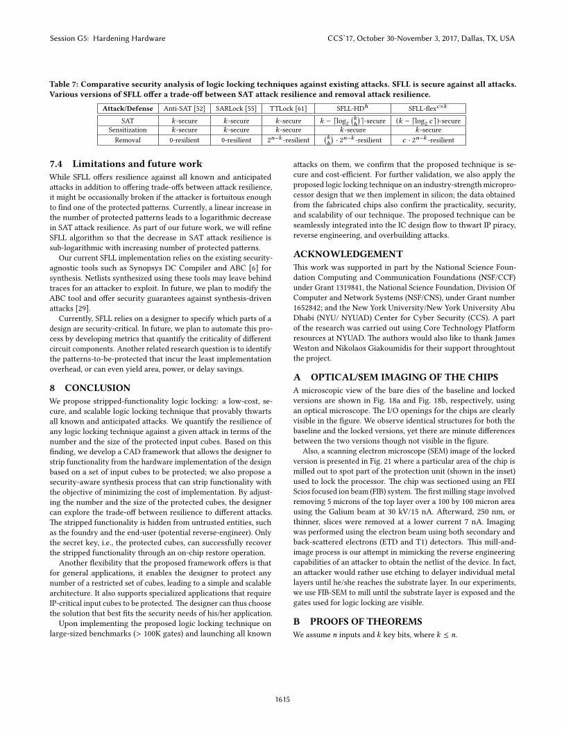
Table 7: Comparative security analysis of logic locking techniques against existing attacks. SFLL is secure against all attacks.Various versions of SFLL o�er a trade-o� between SAT attack resilience and removal attack resilience.
Attack/Defense Anti-SAT [52] SARLock [55] TTLock [61] SFLL-HDh
SFLL-�exc×k
SAT k -secure k -secure k -secure k − dlog2
(kh)e-secure (k − dlog
2c e)-secure
Sensitization k -secure k -secure k -secure k -secure k -secure
Removal 0-resilient 0-resilient 2n−k
-resilient
(kh)· 2n−k -resilient c · 2n−k -resilient
7.4 Limitations and future workWhile SFLL o�ers resilience against all known and anticipated
a�acks in addition to o�ering trade-o�s between a�ack resilience,
it might be occasionally broken if the a�acker is fortuitous enough
to �nd one of the protected pa�erns. Currently, a linear increase in
the number of protected pa�erns leads to a logarithmic decrease
in SAT a�ack resilience. As part of our future work, we will re�ne
SFLL algorithm so that the decrease in SAT a�ack resilience is
sub-logarithmic with increasing number of protected pa�erns.
Our current SFLL implementation relies on the existing security-
agnostic tools such as Synopsys DC Compiler and ABC [6] for
synthesis. Netlists synthesized using these tools may leave behind
traces for an a�acker to exploit. In future, we plan to modify the
ABC tool and o�er security guarantees against synthesis-driven
a�acks [29].
Currently, SFLL relies on a designer to specify which parts of a
design are security-critical. In future, we plan to automate this pro-
cess by developing metrics that quantify the criticality of di�erent
circuit components. Another related research question is to identify
the pa�erns-to-be-protected that incur the least implementation
overhead, or can even yield area, power, or delay savings.
8 CONCLUSIONWe propose stripped-functionality logic locking: a low-cost, se-
cure, and scalable logic locking technique that provably thwarts
all known and anticipated a�acks. We quantify the resilience of
any logic locking technique against a given a�ack in terms of the
number and the size of the protected input cubes. Based on this
�nding, we develop a CAD framework that allows the designer to
strip functionality from the hardware implementation of the design
based on a set of input cubes to be protected; we also propose a
security-aware synthesis process that can strip functionality with
the objective of minimizing the cost of implementation. By adjust-
ing the number and the size of the protected cubes, the designer
can explore the trade-o� between resilience to di�erent a�acks.
�e stripped functionality is hidden from untrusted entities, such
as the foundry and the end-user (potential reverse-engineer). Only
the secret key, i.e., the protected cubes, can successfully recover
the stripped functionality through an on-chip restore operation.
Another �exibility that the proposed framework o�ers is that
for general applications, it enables the designer to protect any
number of a restricted set of cubes, leading to a simple and scalable
architecture. It also supports specialized applications that require
IP-critical input cubes to be protected. �e designer can thus choose
the solution that best �ts the security needs of his/her application.
Upon implementing the proposed logic locking technique on
large-sized benchmarks (> 100K gates) and launching all known
a�acks on them, we con�rm that the proposed technique is se-
cure and cost-e�cient. For further validation, we also apply the
proposed logic locking technique on an industry-strength micropro-
cessor design that we then implement in silicon; the data obtained
from the fabricated chips also con�rm the practicality, security,
and scalability of our technique. �e proposed technique can be
seamlessly integrated into the IC design �ow to thwart IP piracy,
reverse engineering, and overbuilding a�acks.
ACKNOWLEDGEMENT�is work was supported in part by the National Science Foun-
dation Computing and Communication Foundations (NSF/CCF)
under Grant 1319841, the National Science Foundation, Division Of
Computer and Network Systems (NSF/CNS), under Grant number
1652842; and the New York University/New York University Abu
Dhabi (NYU/ NYUAD) Center for Cyber Security (CCS). A part
of the research was carried out using Core Technology Platform
resources at NYUAD. �e authors would also like to thank James
Weston and Nikolaos Giakoumidis for their support throughtout
the project.
A OPTICAL/SEM IMAGING OF THE CHIPSA microscopic view of the bare dies of the baseline and locked
versions are shown in Fig. 18a and Fig. 18b, respectively, using
an optical microscope. �e I/O openings for the chips are clearly
visible in the �gure. We observe identical structures for both the
baseline and the locked versions, yet there are minute di�erences
between the two versions though not visible in the �gure.
Also, a scanning electron microscope (SEM) image of the locked
version is presented in Fig. 21 where a particular area of the chip is
milled out to spot part of the protection unit (shown in the inset)
used to lock the processor. �e chip was sectioned using an FEI
Scios focused ion beam (FIB) system. �e �rst milling stage involved
removing 5 microns of the top layer over a 100 by 100 micron area
using the Galium beam at 30 kV/15 nA. A�erward, 250 nm, or
thinner, slices were removed at a lower current 7 nA. Imaging
was performed using the electron beam using both secondary and
back-sca�ered electrons (ETD and T1) detectors. �is mill-and-
image process is our a�empt in mimicking the reverse engineering
capabilities of an a�acker to obtain the netlist of the device. In fact,
an a�acker would rather use etching to delayer individual metal
layers until he/she reaches the substrate layer. In our experiments,
we use FIB-SEM to mill until the substrate layer is exposed and the
gates used for logic locking are visible.
B PROOFS OF THEOREMSWe assume n inputs and k key bits, where k ≤ n.
Session G5: Hardening Hardware CCS’17, October 30-November 3, 2017, Dallas, TX, USA
1615
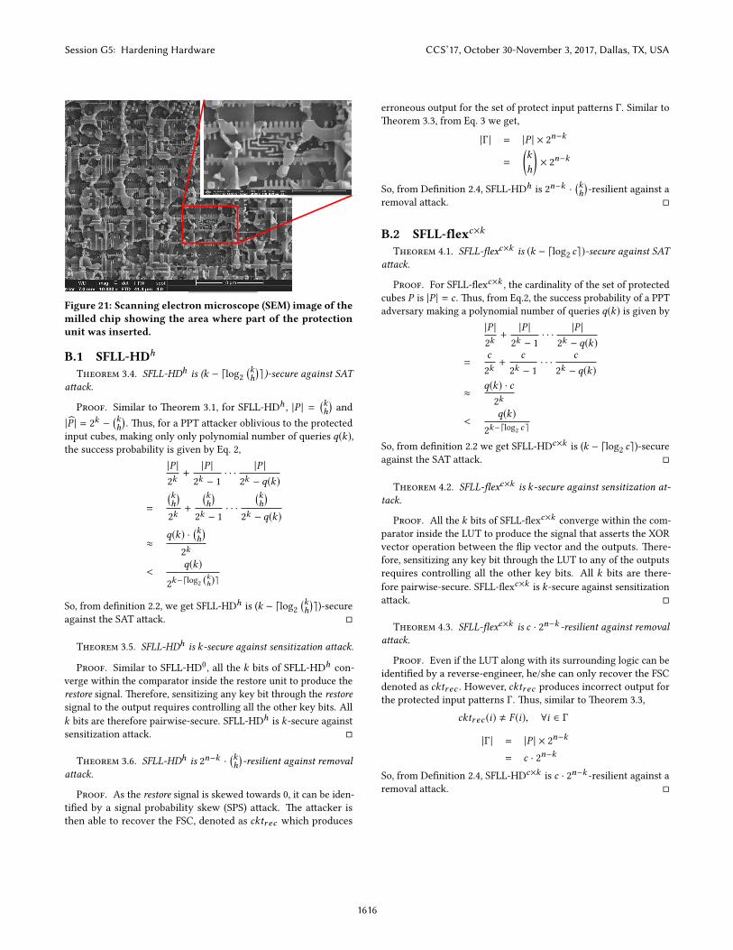
Figure 21: Scanning electronmicroscope (SEM) image of themilled chip showing the area where part of the protectionunit was inserted.
B.1 SFLL-HDh
Theorem 3.4. SFLL-HDh is (k − dlog2
(kh)e)-secure against SAT
a�ack.
Proof. Similar to �eorem 3.1, for SFLL-HDh
, |P | =(kh)
and
|P | = 2k −
(kh). �us, for a PPT a�acker oblivious to the protected
input cubes, making only only polynomial number of queries q(k),the success probability is given by Eq. 2,
|P |2k+|P |
2k − 1
· · · |P |2k − q(k)
=
(kh)
2k+
(kh)
2k − 1
· · ·(kh)
2k − q(k)
≈q(k) ·
(kh)
2k
<q(k)
2k−dlog
2(kh)e
So, from de�nition 2.2, we get SFLL-HDh
is (k − dlog2
(kh)e)-secure
against the SAT a�ack. �
Theorem 3.5. SFLL-HDh is k-secure against sensitization a�ack.
Proof. Similar to SFLL-HD0, all the k bits of SFLL-HD
hcon-
verge within the comparator inside the restore unit to produce the
restore signal. �erefore, sensitizing any key bit through the restoresignal to the output requires controlling all the other key bits. All
k bits are therefore pairwise-secure. SFLL-HDh
is k-secure against
sensitization a�ack. �
Theorem 3.6. SFLL-HDh is 2n−k ·
(kh)-resilient against removal
a�ack.
Proof. As the restore signal is skewed towards 0, it can be iden-
ti�ed by a signal probability skew (SPS) a�ack. �e a�acker is
then able to recover the FSC, denoted as cktr ec which produces
erroneous output for the set of protect input pa�erns Γ. Similar to
�eorem 3.3, from Eq. 3 we get,
|Γ | = |P | × 2n−k
=
(k
h
)× 2
n−k
So, from De�nition 2.4, SFLL-HDh
is 2n−k ·
(kh)-resilient against a
removal a�ack. �
B.2 SFLL-�exc×kTheorem 4.1. SFLL-�exc×k is (k − dlog
2ce)-secure against SAT
a�ack.
Proof. For SFLL-�exc×k
, the cardinality of the set of protected
cubes P is |P | = c . �us, from Eq.2, the success probability of a PPT
adversary making a polynomial number of queries q(k) is given by
|P |2k+|P |
2k − 1
· · · |P |2k − q(k)
=c
2k+
c
2k − 1
· · · c
2k − q(k)
≈ q(k) · c2k
<q(k)
2k−dlog
2c e
So, from de�nition 2.2 we get SFLL-HDc×k
is (k − dlog2ce)-secure
against the SAT a�ack. �
Theorem 4.2. SFLL-�exc×k is k-secure against sensitization at-tack.
Proof. All the k bits of SFLL-�exc×k
converge within the com-
parator inside the LUT to produce the signal that asserts the XOR
vector operation between the �ip vector and the outputs. �ere-
fore, sensitizing any key bit through the LUT to any of the outputs
requires controlling all the other key bits. All k bits are there-
fore pairwise-secure. SFLL-�exc×k
is k-secure against sensitization
a�ack. �
Theorem 4.3. SFLL-�exc×k is c · 2n−k -resilient against removala�ack.
Proof. Even if the LUT along with its surrounding logic can be
identi�ed by a reverse-engineer, he/she can only recover the FSC
denoted as cktr ec . However, cktr ec produces incorrect output for
the protected input pa�erns Γ. �us, similar to �eorem 3.3,
cktr ec (i) , F (i), ∀i ∈ Γ|Γ | = |P | × 2
n−k
= c · 2n−k
So, from De�nition 2.4, SFLL-HDc×k
is c · 2n−k -resilient against a
removal a�ack. �
Session G5: Hardening Hardware CCS’17, October 30-November 3, 2017, Dallas, TX, USA
1616

REFERENCES[1] Y. Alkabani and F. Koushanfar. 2007. Active Hardware Metering for Intellectual
Property Protection and Security. In USENIX Security. 291–306.
[2] ARM. 2013. Cortex-M0 Processor. (2013). h�ps://www.arm.com/products/
processors/cortex-m/cortex-m0.php
[3] J.P. Baukus, L.W. Chow, R.P. Cocchi, P.O., and B.J. Wang. 2012. Building Block
for a Secure CMOS Logic Cell Library. (2012). US Patent no. 8111089.
[4] J.P. Baukus, L.W. Chow, R.P. Cocchi, and B.J. Wang. 2012. Method and Apparatus
for Camou�aging a Standard Cell based Integrated Circuit with Micro Circuits
and Post Processing. (2012). US Patent no. 20120139582.
[5] A. Baumgarten, A. Tyagi, and J. Zambreno. 2010. Preventing IC Piracy Using
Recon�gurable Logic Barriers. IEEE Des. Test. Comput. 27, 1 (2010), 66–75.
[6] R. Brayton and A. Mishchenko. 2010. ABC: An Academic Industrial-strength
Veri�cation Tool. In International Conference on Computer Aided Veri�cation.
Springer, 24–40.
[7] F. Brglez, D. Bryan, and K. Kozminski. 1989. Combinational Pro�les of Sequential
Benchmark Circuits. In IEEE International Symposium on Circuits and Systems.1929–1934.
[8] Q. Chen, A. M. Azab, G. Ganesh, and P. Ning. 2017. PrivWatcher: Non-bypassable
Monitoring and Protection of Process Credentials from Memory Corruption
A�acks. In ACM Asia Conference on Computer and Communications Security.
167–178.
[9] Chipworks. 2012. Intel‘s 22-nm Tri-gate Transistors Exposed.
h�p://www.chipworks.com/blog/technologyblog/2012/04/23/intels-22-
nm-tri-gate-transistors-exposed/. (2012).
[10] S. Chu and C Burrus. 1984. Multirate �lter designs using comb �lters. IEEETransactions on Circuits and Systems 31, 11 (1984), 913–924.
[11] S. Davidson. 1999. Notes on ITC’99 Benchmarks. h�p://www.cerc.utexas.edu/
itc99-benchmarks/bendoc1.html. (1999).
[12] J. Diguet, S. Evain, R. Vaslin, G. Gogniat, and E. Juin. 2007. NOC-centric security
of recon�gurable SoC. In IEEE First International Symposium on Networks-on-Chip.
223–232.
[13] C. Helfmeier, D. Nedospasov, C. Tarnovsky, J.S. Krissler, C. Boit, and J.P. Seifert.
2013. Breaking and Entering through the Silicon. In ACM SIGSAC Conference onComputer and Communications Security. 733–744.
[14] F. Imeson, A. Emtenan, S. Garg, and M. V. Tripunitara. 2013. Securing Computer
Hardware Using 3D Integrated Circuit (IC) Technology and Split Manufacturing
for Obfuscation. In USENIX Conference on Security. 495–510.
[15] Maxim Integrated. 2010. DeepCover Security Manager for Low-Voltage
Operation with 1KB Secure Memory and Programmable Tamper Hier-
archy. h�ps://www.maximintegrated.com/en/products/power/supervisors-
voltage-monitors-sequencers/DS3660.html/tb tab0. (2010).
[16] R.W. Jarvis and M.G. McIntyre. 2007. Split Manufacturing Method for Advanced
Semiconductor Circuits. (2007). US Patent 7,195,931.
[17] A.B. Kahng, J. Lach, W. H Mangione-Smith, S. Mantik, I.L. Markov, M. Potkonjak,
P. Tucker, H. Wang, and G. Wolfe. 1998. Watermarking Techniques for Intellectual
Property Protection. In IEEE/ACM Design Automation Conference. 776–781.
[18] A.B. Kahng, S. Mantik, I.L. Markov, M. Potkonjak, P. Tucker, Huijuan Wang,
and G. Wolfe. 1998. Robust IP watermarking methodologies for physical design.
Design Automation Conference (1998), 782–787.
[19] M. Kammerste�er, M. Muellner, D. Burian, D. Platzer, and W. Kastner. 2014.
Breaking Integrated Circuit Device Security �rough Test Mode Silicon Reverse
Engineering. In ACM SIGSAC Conference on Computer and CommunicationsSecurity. 549–557.
[20] R. Karri, J. Rajendran, K. Rosenfeld, and M. Tehranipoor. 2010. Trustworthy
Hardware: Identifying and Classifying Hardware Trojans. Computer 43, 10
(2010), 39–46.
[21] D. Kirovski and M. Potkonjak. 2003. Local watermarks: methodology and appli-
cation to behavioral synthesis. IEEE Transactions on Computer-Aided Design ofIntegrated Circuits and Systems 22, 9 (2003), 1277–1283.
[22] F. Koushanfar. 2012. Provably Secure Active IC Metering Techniques for Piracy
Avoidance and Digital Rights Management. IEEE Trans. Inf. Forensics Security 7,
1 (2012), 51–63.
[23] F. Koushanfar and G. �. 2001. Hardware Metering. In IEEE/ACM Design Au-tomation Conference. 490–493.
[24] S. Kumar, S. Dharmapurikar, F. Yu, P. Crowley, and J. Turner. 2006. Algorithms
to accelerate multiple regular expressions matching for deep packet inspection.
In ACM SIGCOMM Computer Communication Review, Vol. 36. 339–350.
[25] H.K. Lee and D.S. Ha. 1993. Atalanta: an E�cient ATPG for Combinational
Circuits. In Technical Report.[26] S. Leef. 2017. In Pursuit of Secure Silicon. h�p://textlab.io/doc/22959027/mr.-
serge-leef--vp-new-ventures--mentor-graphics. (2017).
[27] M. Li, K. Shamsi, T. Meade, Z. Zhao, B. Yu, Y. Jin, and D.Z. Pan. 2016. Provably
Secure Camou�aging Strategy for IC Protection. In IEEE/ACM InternationalConference on Computer-Aided Design. 28:1–28:8.
[28] M.E. Massad, S. Garg, and M.V. Tripunitara. 2015. Integrated Circuit (IC) Decam-
ou�aging: Reverse Engineering Camou�aged ICs within Minutes. In Network
and Distributed System Security Symposium.
[29] M.E. Massad, J. Zhang, S. Garg, and M.V. Tripunitara. 2017. Logic Locking for
Secure Outsourced Chip Fabrication: A New A�ack and Provably Secure Defense
Mechanism. CoRR abs/1703.10187 (2017). h�p://arxiv.org/abs/1703.10187
[30] E.J. McCluskey. 1956. Minimization of Boolean functions. Bell System TechnicalJournal 35, 6 (1956), 1417–1444.
[31] A.L. Oliveira. 1999. Robust Techniques for Watermarking Sequential Circuit
Designs. In IEEE/ACM Design Automation Conference. 837–842.
[32] T. S. Perry. 2017. Why Hardware Engineers Have to �ink Like Cybercriminals,
and Why Engineers Are Easy to Fool. (2017). h�p://spectrum.ieee.org/view-
from-the-valley/computing/embedded-systems/why-hardware-engineers-
have-to-think-like-cybercriminals-and-why-engineers-are-easy-to-fool
[33] S.M. Plaza and I.L. Markov. 2015. Solving the �ird-Shi� Problem in IC Piracy
With Test-Aware Logic Locking. IEEE Transactions on CAD of Integrated Circuitsand Systems 34, 6 (2015), 961–971.
[34] J. Rajendran, Y. Pino, O. Sinanoglu, and R. Karri. 2012. Security Analysis of Logic
Obfuscation. In IEEE/ACM Design Automation Conference. 83–89.
[35] J. Rajendran, M. Sam, O. Sinanoglu, and R. Karri. 2013. Security Analysis of
Integrated Circuit Camou�aging. In ACM/SIGSAC Conference on Computer &Communications Security. 709–720.
[36] J. Rajendran, Huan Zhang, Chi Zhang, G.S. Rose, Youngok Pino, O. Sinanoglu,
and R. Karri. 2015. Fault Analysis-Based Logic Encryption. IEEE Transactions onComputer 64, 2 (2015), 410–424.
[37] M. Rostami, F. Koushanfar, and R. Karri. 2014. A Primer on Hardware Security:
Models, Methods, and Metrics. IEEE 102, 8 (2014), 1283–1295.
[38] J.A. Roy, F. Koushanfar, and Igor L Markov. 2010. Ending Piracy of Integrated
Circuits. IEEE Computer 43, 10 (2010), 30–38.
[39] SEMI. 2008. Innovation is at Risk Losses of up to $4 Billion Annually due to IP
Infringement. (2008). www.semi.org/en/Issues/IntellectualProperty/ssLINK/
P043785 [June 10, 2015].
[40] K. Shamsi, M. Li, T. Meade, Z. Zhao, D.P. Z., and Y. Jin. 2017. AppSAT: Approx-
imately Deobfuscating Integrated Circuits. In to appear in IEEE InternationalSymposium on Hardware Oriented Security and Trust.
[41] Y. Shen and H. Zhou. 2017. Double DIP: Re-Evaluating Security of Logic
Encryption Algorithms. Cryptology ePrint Archive, Report 2017/290. (2017).
h�p://eprint.iacr.org/2017/290.
[42] J. P. Skudlarek, T. Katsioulas, and M. Chen. 2016. A Platform Solution for Secure
Supply-Chain and Chip Life-Cycle Management. Computer 49, 8 (2016), 28–34.
[43] J.E. Stine, I. Castellanos, M. Wood, J. Henson, F. Love, W.R. Davis, P. D Franzon, M.
Bucher, S. Basavarajaiah, J. Oh, et al. 2007. FreePDK: An Open-Source Variation-
Aware Design Kit. In IEEE International Conference on Microelectronic SystemsEducation. 173–174.
[44] P. Subramanyan, S. Ray, and S. Malik. 2015. Evaluating the Security of Logic
Encryption Algorithms. In IEEE International Symposium on Hardware OrientedSecurity and Trust. 137–143.
[45] P. Subramanyan, N. Tsiskaridze, K. Pasricha, D. Reisman, A. Susnea, and S. Malik.
2013. Reverse Engineering Digital Circuits Using Functional Analysis. IEEE/ACMDesign Automation and Test in Europe (2013).
[46] SypherMedia. 2017. SypherMedia Library Circuit Camou�age Technology. h�p://
www.smi.tv/syphermedia library circuit camou�age technology.html. (2017).
[47] TechInsights. 2017. Samsung Galaxy S8 (SM-G950W) Teardown.
h�p://www.techinsights.com/about-techinsights/overview/blog/samsung-
galaxy-s8-teardown. (2017).
[48] M. M. Tehranipoor, U. Guin, and S. Bhunia. 2017. Invasion of the Hardware
Snatchers. IEEE Spectrum 54, 5 (2017), 36–41.
[49] R. Torrance and D. James. 2011. �e State-of-the-Art in Semiconductor Reverse
Engineering. In IEEE/ACM Design Automation Conference. 333–338.
[50] P. Tuyls, G. Schrijen, B. Skoric, J. van Geloven, N. Verhaegh, and R. Wolters.
2006. Read-Proof Hardware from Protective Coatings. In International Conferenceon Cryptographic Hardware and Embedded Systems, Louis Goubin and Mitsuru
Matsui (Eds.). 369–383.
[51] A. Vijayakumar, V.C. Patil, D.E. Holcomb, C. Paar, and S. Kundu. 2017. Physical
Design Obfuscation of Hardware: A Comprehensive Investigation of Device and
Logic-Level Techniques. IEEE Transactions on Information Forensics and Security12, 1 (2017), 64–77.
[52] Y. Xie and A. Srivastava. 2016. Mitigating SAT A�ack on Logic Locking. In
International Conference on Cryptographic Hardware and Embedded Systems. 127–
146.
[53] X. Xu, B. Shakya, M.M. Tehranipoor, and D. Forte. 2017. Novel Bypass A�ack
and BDD-based Tradeo� Analysis Against all Known Logic Locking A�acks.
Cryptology ePrint Archive, Report 2017/621. (2017). h�p://eprint.iacr.org/2017/
621.
[54] M. Yasin, B. Mazumdar, S. S. Ali, and O. Sinanoglu. 2015. Security Analysis of
Logic Encryption against the Most E�ective Side-Channel A�ack: DPA. In IEEEInternational Symposium onDefect and Fault Tolerance in VLSI andNanotechnologySystems. 97–102.
[55] M. Yasin, B. Mazumdar, J. Rajendran, and O. Sinanoglu. 2016. SARLock: SAT
A�ack Resistant Logic Locking. In IEEE International Symposium on Hardware
Session G5: Hardening Hardware CCS’17, October 30-November 3, 2017, Dallas, TX, USA
1617
Oriented Security and Trust. 236–241.
[56] M. Yasin, B. Mazumdar, O. Sinanoglu, and J. Rajendran. 2016. CamoPerturb:
Secure IC Camou�aging for Minterm Protection. IEEE/ACM International Con-ference on Computer-Aided Design, 29:1–29:8.
[57] M. Yasin, B. Mazumdar, O. Sinanoglu, and J. Rajendran. 2016. Security Analysis
of Anti-SAT. IEEE Asia and South Paci�c Design Automation Conference (2016),
342–347.
[58] M. Yasin, B. Mazumdar, O. Sinanoglu, and J. Rajendran. 2017. Removal A�acks
on Logic Locking and Camou�aging Techniques. IEEE Transactions on EmergingTopics in Computing 99, 0 (2017), PP.
[59] M. Yasin, J. Rajendran, O. Sinanoglu, and R. Karri. 2016. On Improving the
Security of Logic Locking. IEEE Transactions on CAD of Integrated Circuits andSystems 35, 9 (2016), 1411–1424.
[60] M. Yasin, S. M. Saeed, J. Rajendran, and O. Sinanoglu. 2016. Activation of Logic
Encrypted Chips: Pre-test or Post-Test?. In Design, Automation Test in Europe.139–144.
[61] M. Yasin, A. Sengupta, B.C. Schafer, Y. Makris, O. Sinanoglu, and J. Rajendran.
2017. What to Lock?: Functional and Parametric Locking. In Great Lakes Sympo-sium on VLSI. 351–356.
[62] M. Yasin, O. Sinanoglu, and J. Rajendran. 2017. Testing the Trustworthiness of
IC Testing: An Oracle-Less A�ack on IC Camou�aging. IEEE Transactions onInformation Forensics and Security 12, 11 (2017), 2668–2682.
[63] M. Yasin, T. Tekeste, H. Saleh, B. Mohammad, O. Sinanoglu, and M. Ismail. 2017.
Ultra-Low Power, Secure IoT Platform for Predicting Cardiovascular Diseases.
IEEE Transactions on Circuits and Systems I: Regular Papers PP, 99 (2017), 1–14.
Session G5: Hardening Hardware CCS’17, October 30-November 3, 2017, Dallas, TX, USA
1618