proximity sensing of up to 30-cm range with >15-db snr ... multiple proximity sensors, the design...
TRANSCRIPT
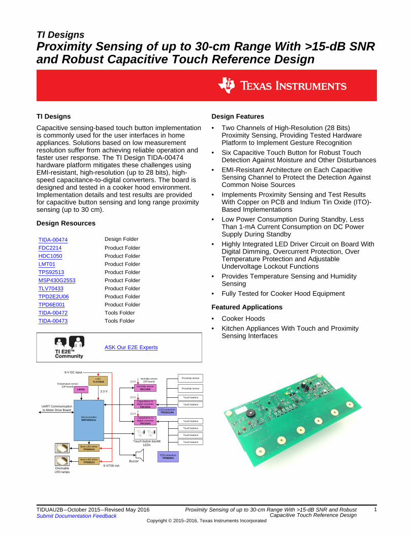
Buck LED driverTPS92513
LMT01
Capacitance to digital converter
FDC2214
DimmableLED lamps
UART Communication to Motor Drive Board
LDOTLV70433
9-V DC input
ESD protectionTPD2E2U06
Proximity sensor
Touch buttons
Touch buttons
Touch buttons
Touch buttons
Touch buttons
Touch buttonsTouch button backlit LEDs
9 V/700 mA
3.3 V
Temperature sensor(Off board)
Buzzer
Proximity sensor
MicrocontrollerMSP430G2xx
Humidity sensor HDC1050
3.3 V
3.3 V
3.3 V
Capacitance to digital converter
FDC2214
Buck LED driverTPS92513
ESD protectionTPD6E001
Humidity sensor(Off board)
LCD LCD
1TIDUAU2B–October 2015–Revised May 2016Submit Documentation Feedback
Copyright © 2015–2016, Texas Instruments Incorporated
Proximity Sensing of up to 30-cm Range With >15-dB SNR and RobustCapacitive Touch Reference Design
TI DesignsProximity Sensing of up to 30-cm Range With >15-dB SNRand Robust Capacitive Touch Reference Design
TI DesignsCapacitive sensing-based touch button implementationis commonly used for the user interfaces in homeappliances. Solutions based on low measurementresolution suffer from achieving reliable operation andfaster user response. The TI Design TIDA-00474hardware platform mitigates these challenges usingEMI-resistant, high-resolution (up to 28 bits), high-speed capacitance-to-digital converters. The board isdesigned and tested in a cooker hood environment.Implementation details and test results are providedfor capacitive button sensing and long range proximitysensing (up to 30 cm).
Design Resources
TIDA-00474 Design FolderFDC2214 Product FolderHDC1050 Product FolderLMT01 Product FolderTPS92513 Product FolderMSP430G2553 Product FolderTLV70433 Product FolderTPD2E2U06 Product FolderTPD6E001 Product FolderTIDA-00472 Tools FolderTIDA-00473 Tools Folder
ASK Our E2E Experts
Design Features• Two Channels of High-Resolution (28 Bits)
Proximity Sensing, Providing Tested HardwarePlatform to Implement Gesture Recognition
• Six Capacitive Touch Button for Robust TouchDetection Against Moisture and Other Disturbances
• EMI-Resistant Architecture on Each CapacitiveSensing Channel to Protect the Detection AgainstCommon Noise Sources
• Implements Proximity Sensing and Test ResultsWith Copper on PCB and Indium Tin Oxide (ITO)-Based Implementations
• Low Power Consumption During Standby, LessThan 1-mA Current Consumption on DC PowerSupply During Standby
• Highly Integrated LED Driver Circuit on Board WithDigital Dimming, Overcurrent Protection, OverTemperature Protection and AdjustableUndervoltage Lockout Functions
• Provides Temperature Sensing and HumiditySensing
• Fully Tested for Cooker Hood Equipment
Featured Applications• Cooker Hoods• Kitchen Appliances With Touch and Proximity
Sensing Interfaces
Key System Specifications www.ti.com
2 TIDUAU2B–October 2015–Revised May 2016Submit Documentation Feedback
Copyright © 2015–2016, Texas Instruments Incorporated
Proximity Sensing of up to 30-cm Range With >15-dB SNR and RobustCapacitive Touch Reference Design
An IMPORTANT NOTICE at the end of this TI reference design addresses authorized use, intellectual property matters and otherimportant disclaimers and information.
1 Key System Specifications
Table 1. Key System Specifications
PARAMETER SPECIFICATION COMMENTCapacitive sensor type Copper on PCB, ITO sensor on glass
Input voltage 9-V nominal Refer to TIDA-00473 for power supplydesign reference
Proximity sensing range 30 cm for static sensing5 to 15 cm for gesture sensingSample rate >30 SPS for proximity sensingCalibration method Dynamic baseline tracingLED lamps voltage, current 350 mALED driver switching frequency 1 MHzLED dimming PWM frequency 250 HzOperating temperature –40°C to 85°C Device specificationExternal sensors for cooker hoodapplication Temperature and humidity
Standby current 0.89 mA on 3.3-V rail (with one-secondwake-up period)
Tests
Proximity sensing performance tested withsteam disturbances and inside an actualcooker hoodTouch button performance tested withwater on surface
Debugging communication port UART or Spy-Bi-Wire™
r 0 AC
d
e ´ e ´
=
www.ti.com System Description
3TIDUAU2B–October 2015–Revised May 2016Submit Documentation Feedback
Copyright © 2015–2016, Texas Instruments Incorporated
Proximity Sensing of up to 30-cm Range With >15-dB SNR and RobustCapacitive Touch Reference Design
2 System DescriptionThis system is designed for the human machine interface application in cooker hood end equipment withproximity sensing, touch buttons, and dimmable LED lamp driving functions. Together with humidity andtemperature sensors provided in this platform, one can implement the automatic speed control of themotor drive based on the temperature and the conditions of the air under the hood.
The proximity sensing feature of the design can be used for both wake-up from standby and gesturerecognition functionalities to the end equipment. This feature is enabled by Texas Instruments’ high-resolution capacitive-to-digital converter. The design is able to achieve a 30-cm distance of proximitysensing at static status. With multiple proximity sensors, the design also provides gesture recognitionfunctions to the system, bringing a hand-free experience to the end users.
The design supports up to six touch buttons with EMI-robust capacitance sensing channels. The highresolution and EMI robust capacitance-to-digital converter enables the touch buttons to operate reliably inharsh environment conditions such as steam, water, and oily surfaces that are common in cooker hoodapplications.
A dimmable LED lighting function is also integrated into the design with two individual channels of highlyintegrated LED drivers, which can be controlled separately by digital PWM dimming.
This design guide covers component selection, quick starting with the firmware, and test results.
2.1 Capacitive SensingCapacitive sensing is becoming a popular technology to replace optical detection methods andmechanical designs for applications like proximity and gesture detection, material analysis, and liquid levelsensing. The main advantages capacitive sensing has over other detection approaches are that it cansense different kinds of materials (skin, plastic, metal, liquid), it is contactless and wear-free, it has theability to sense up to a large distance with small sensor sizes, the PCB sensor is low cost, and it is a lowpower solution.
Before discussing the equivalent circuit, some basic terms are introduced: electrode, traces, andcapacitance.
An electrode is the physical conductive structure that a person interacts with. This structure is typicallythought of as the copper on a printed circuit board (PCB), but can also be made of transparent materialssuch as indium tin oxide (ITO) or other conductive materials like silver. This design guide shows theperformance of using an ITO electrode as a proximity sensor for cooker hood applications.
A trace is the conductive connection between the capacitance-to-digital convertor and the electrode.Similar to the electrode, the trace is typically a copper trace on a PCB or copper cable from the PCB tothe sensor plate, but it could also be made of materials like ITO and silver.
Capacitance is the ability of a capacitor to store an electrical charge. A common form—a parallel platecapacitor—the capacitance is calculated by C = Q / V, where C is the capacitance related by the storedcharge Q at a given voltage V. The capacitance (measured in Farads) of a parallel plate capacitor consistsof two conductor plates and is calculated by:
(1)
where• A is the area of the two plates (in meters)• εr is the dielectric constant of the material between the plates• ε0 is the permittivity of free space (8.85 × 10 – 12 F/m)• d is the separation between the plates (in meters)
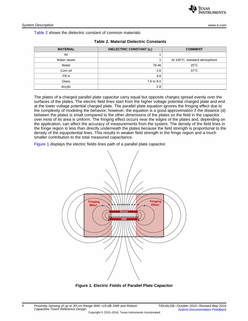
Sensor
GND
Fringing
Effect
Fringing
Effect
System Description www.ti.com
4 TIDUAU2B–October 2015–Revised May 2016Submit Documentation Feedback
Copyright © 2015–2016, Texas Instruments Incorporated
Proximity Sensing of up to 30-cm Range With >15-dB SNR and RobustCapacitive Touch Reference Design
Table 2 shows the dielectric constant of common materials:
Table 2. Material Dielectric Constants
MATERIAL DIELECTRIC CONSTANT (εr) COMMENTAir 1
Water steam 1 At 100°C, standard atmosphereWater 78.46 25°C
Corn oil 2.6 37°CFR-4 4.8Glass 7.6 to 8.0Acrylic 2.8
The plates of a charged parallel plate capacitor carry equal but opposite charges spread evenly over thesurfaces of the plates. The electric field lines start from the higher voltage potential charged plate and endat the lower voltage potential charged plate. The parallel plate equation ignores the fringing effect due tothe complexity of modeling the behavior; however, the equation is a good approximation if the distance (d)between the plates is small compared to the other dimensions of the plates so the field in the capacitorover most of its area is uniform. The fringing effect occurs near the edges of the plates and, depending onthe application, can affect the accuracy of measurements from the system. The density of the field lines inthe fringe region is less than directly underneath the plates because the field strength is proportional to thedensity of the equipotential lines. This results in weaker field strength in the fringe region and a muchsmaller contribution to the total measured capacitance.
Figure 1 displays the electric fields lines path of a parallel plate capacitor.
Figure 1. Electric Fields of Parallel Plate Capacitor
Csense
CelectrodeCtraceCparasitics
CgroundLocal
Ground EarthGround
www.ti.com System Description
5TIDUAU2B–October 2015–Revised May 2016Submit Documentation Feedback
Copyright © 2015–2016, Texas Instruments Incorporated
Proximity Sensing of up to 30-cm Range With >15-dB SNR and RobustCapacitive Touch Reference Design
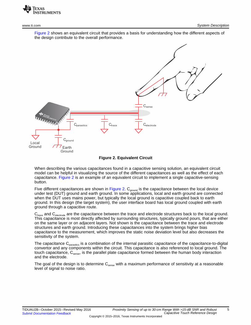
Figure 2 shows an equivalent circuit that provides a basis for understanding how the different aspects ofthe design contribute to the overall performance.
Figure 2. Equivalent Circuit
When describing the various capacitances found in a capacitive sensing solution, an equivalent circuitmodel can be helpful in visualizing the source of the different capacitances as well as the effect of eachcapacitance. Figure 2 is an example of an equivalent circuit to implement a single capacitive-sensingbutton.
Five different capacitances are shown in Figure 2. Cground is the capacitance between the local deviceunder test (DUT) ground and earth ground. In some applications, local and earth ground are connectedwhen the DUT uses mains power, but typically the local ground is capacitive coupled back to earthground. In this design (the target system), the user interface board has local ground coupled with earthground through a capacitive route.
Ctrace and Celectrode are the capacitance between the trace and electrode structures back to the local ground.This capacitance is most directly affected by surrounding structures, typically ground pours, that are eitheron the same layer or on adjacent layers. Not shown is the capacitance between the trace and electrodestructures and earth ground. Introducing these capacitances into the system brings higher biascapacitance to the measurement, which improves the static noise deviation level but also decreases thesensitivity of the system.
The capacitance Cparasitics is a combination of the internal parasitic capacitance of the capacitance-to-digitalconvertor and any components within the circuit. This capacitance is also referenced to local ground. Thetouch capacitance, Csense, is the parallel plate capacitance formed between the human body interactionand the electrode.
The goal of the design is to determine Csense with a maximum performance of sensitivity at a reasonablelevel of signal to noise ratio.
System Description www.ti.com
6 TIDUAU2B–October 2015–Revised May 2016Submit Documentation Feedback
Copyright © 2015–2016, Texas Instruments Incorporated
Proximity Sensing of up to 30-cm Range With >15-dB SNR and RobustCapacitive Touch Reference Design
2.2 Capacitance-to-Digital ConverterThe key specifications and care about of the capacitance-to-digital converter are low noise, EMIresistance, high resolution, and high-speed conversion. The device should be able to allow large inputcapacitance (nanofarads [nF]) to enable the use of remote sensors and tracking of environmental changesover temperature and humidity. The other desirable features are power saving modes and an interruptfeature on conversion completion. Features such as variable sensor excitation frequency make the systemdesign very flexible.
For proximity detection, the detection range is limited by the minimum capacitance that can be measured.Therefore, a capacitance-to-digital converter with a deep sub-fF measurement capability can detect awider range.
2.3 Humidity and Temperature SensorMeasuring humidity and temperature for capacitive sensing applications helps to compensate the drift ofpassive component values. From a cooker hood system perspective, measuring the temperature andhumidity levels under the hood would help to automatically adjust the suction motor speed and therebyachieve optimal efficiency and lower acoustic operation without much user intervention.
2.4 LED Lamp ControllerIn cooker hoods, lighting is a common requirement, and the lighting can be based on incandescent lamps,Halogen lamps, or LED lamps. With the advent of high power, high luminous efficiency LEDs, using LEDlamps has been increasing. LED lamps help achieve very high efficiency and easily controls PWMdimming. The common requirements of LED driver are integrating PWM control and MOSFETs, highfrequency operation to help reduce the size of Inductor and capacitors, constant current control, andsimple, efficient PWM dimming facility along with protections.
Buck LED driverTPS92513
LMT01
Capacitance to digital converter
FDC2214
DimmableLED lamps
UART Communication to Motor Drive Board
LDOTLV70433
9-V DC input
ESD protectionTPD2E2U06
Proximity sensor
Touch buttons
Touch buttons
Touch buttons
Touch buttons
Touch buttons
Touch buttonsTouch button backlit LEDs
9 V/700 mA
3.3 V
Temperature sensor(Off board)
Buzzer
Proximity sensor
MicrocontrollerMSP430G2xx
Humidity sensor HDC1050
3.3 V
3.3 V
3.3 V
Capacitance to digital converter
FDC2214
Buck LED driverTPS92513
ESD protectionTPD6E001
Humidity sensor(Off board)
LCD LCD
www.ti.com Block Diagram
7TIDUAU2B–October 2015–Revised May 2016Submit Documentation Feedback
Copyright © 2015–2016, Texas Instruments Incorporated
Proximity Sensing of up to 30-cm Range With >15-dB SNR and RobustCapacitive Touch Reference Design
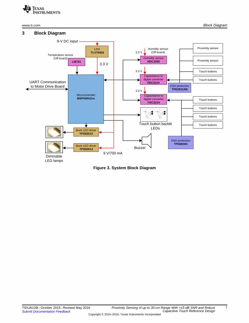
3 Block Diagram
Figure 3. System Block Diagram
IN0A
IN0B
IN3A
IN3B
FDC2214VDD
GND
SCL
SDA
Int. Osc.
ADDR
INTB
SD
GND
MCU
VDD
3.3 V3.3 V
GPIO
GPIO
0.1 F 1 F
Core
I2C
I2C
peripheral
3.3 V
L
Cap
Sensor 0
CLKIN40 MHz
C
L
Cap
Sensor 3
C
Resonant
circuit driver
Resonant
circuit driver
Highlighted Products www.ti.com
8 TIDUAU2B–October 2015–Revised May 2016Submit Documentation Feedback
Copyright © 2015–2016, Texas Instruments Incorporated
Proximity Sensing of up to 30-cm Range With >15-dB SNR and RobustCapacitive Touch Reference Design
4 Highlighted ProductsThe Robust, High-Resolution Capacitive Touch and Proximity Sensing User Interface With LED LightingDesign includes the following devices:• FDC2214: EMI-Resistant 28-Bit Capacitance to Digital Converter• HDC1050: Low Power, 3% Accuracy Digital Humidity Sensor with Integrated Temperature Sensor• LMT01: 0.5°C Accurate 2-pin Temperature Sensor with a Pulse Train Interface• TPS92513: 1.5-A Buck LED Driver with Integrated Analog Current Adjust• MSP430G2553: MSP430G2x53 Mixed Signal Microcontroller• TLV70433: 24-V Input Voltage, 150-mA, Ultralow IQ Low-Dropout Regulators• TPD2E2U06: Dual-Channel High-Speed ESD Protection
For more information on each of these devices, see their respective product folders at www.ti.com.
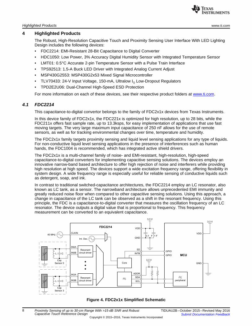
4.1 FDC2214This capacitance-to-digital convertor belongs to the family of FDC2x1x devices from Texas Instruments.
In this device family of FDC2x1x, the FDC221x is optimized for high resolution, up to 28 bits, while theFDC211x offers fast sample rate, up to 13.3ksps, for easy implementation of applications that use fastmoving targets. The very large maximum input capacitance of 250 nF allows for the use of remotesensors, as well as for tracking environmental changes over time, temperature and humidity.
The FDC2x1x family targets proximity sensing and liquid level sensing applications for any type of liquids.For non-conductive liquid level sensing applications in the presence of interferences such as humanhands, the FDC1004 is recommended, which has integrated active shield drivers.
The FDC2x1x is a multi-channel family of noise- and EMI-resistant, high-resolution, high-speedcapacitance-to-digital converters for implementing capacitive sensing solutions. The devices employ aninnovative narrow-band based architecture to offer high rejection of noise and interferers while providinghigh resolution at high speed. The devices support a wide excitation frequency range, offering flexibility insystem design. A wide frequency range is especially useful for reliable sensing of conductive liquids suchas detergent, soap, and ink.
In contrast to traditional switched-capacitance architectures, the FDC2214 employ an LC resonator, alsoknown as LC tank, as a sensor. The narrowband architecture allows unprecedented EMI immunity andgreatly reduced noise floor when compared to other capacitive sensing solutions. Using this approach, achange in capacitance of the LC tank can be observed as a shift in the resonant frequency. Using thisprinciple, the FDC is a capacitance-to-digital converter that measures the oscillation frequency of an LCresonator. The device outputs a digital value that is proportional to frequency. This frequencymeasurement can be converted to an equivalent capacitance.
Figure 4. FDC2x1x Simplified Schematic
GND
MCU
I2C
Peripheral
3.3V
ADC
TEMPERATURE
RH
I2C
Registers
+
Logic
HDC1050
SDASCL
OTP
Calibration Coefficients
VDD
GND
3.3V
VDD
3.3V
www.ti.com Highlighted Products
9TIDUAU2B–October 2015–Revised May 2016Submit Documentation Feedback
Copyright © 2015–2016, Texas Instruments Incorporated
Proximity Sensing of up to 30-cm Range With >15-dB SNR and RobustCapacitive Touch Reference Design
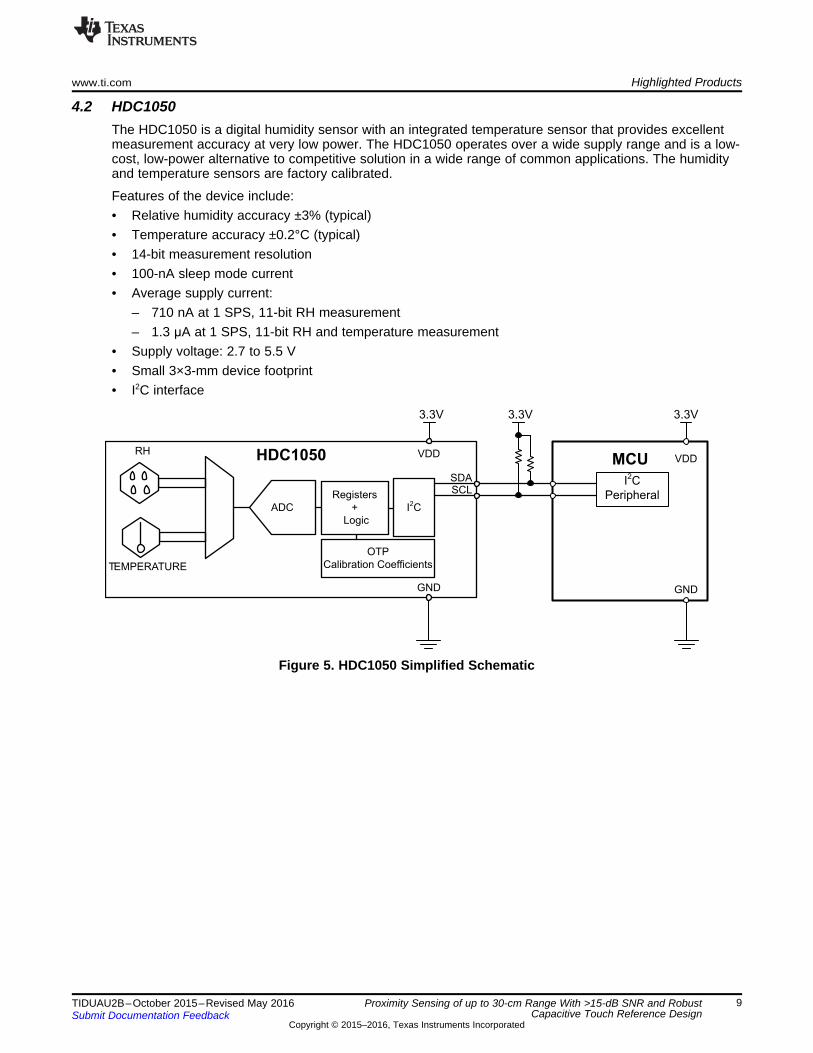
4.2 HDC1050The HDC1050 is a digital humidity sensor with an integrated temperature sensor that provides excellentmeasurement accuracy at very low power. The HDC1050 operates over a wide supply range and is a low-cost, low-power alternative to competitive solution in a wide range of common applications. The humidityand temperature sensors are factory calibrated.
Features of the device include:• Relative humidity accuracy ±3% (typical)• Temperature accuracy ±0.2°C (typical)• 14-bit measurement resolution• 100-nA sleep mode current• Average supply current:
– 710 nA at 1 SPS, 11-bit RH measurement– 1.3 μA at 1 SPS, 11-bit RH and temperature measurement
• Supply voltage: 2.7 to 5.5 V• Small 3×3-mm device footprint• I2C interface
Figure 5. HDC1050 Simplified Schematic
MCU/
FPGA/
ASIC
VDD: 3.0V to 5.5V
GPIO
GPIO/
COMP
LMT01
VP
VN
Up to 2m
Min 2.0V
LMT01 Pulse Count Interface
Power Off
Conversion Time
ADC Conversion Result
Power On
Highlighted Products www.ti.com
10 TIDUAU2B–October 2015–Revised May 2016Submit Documentation Feedback
Copyright © 2015–2016, Texas Instruments Incorporated
Proximity Sensing of up to 30-cm Range With >15-dB SNR and RobustCapacitive Touch Reference Design
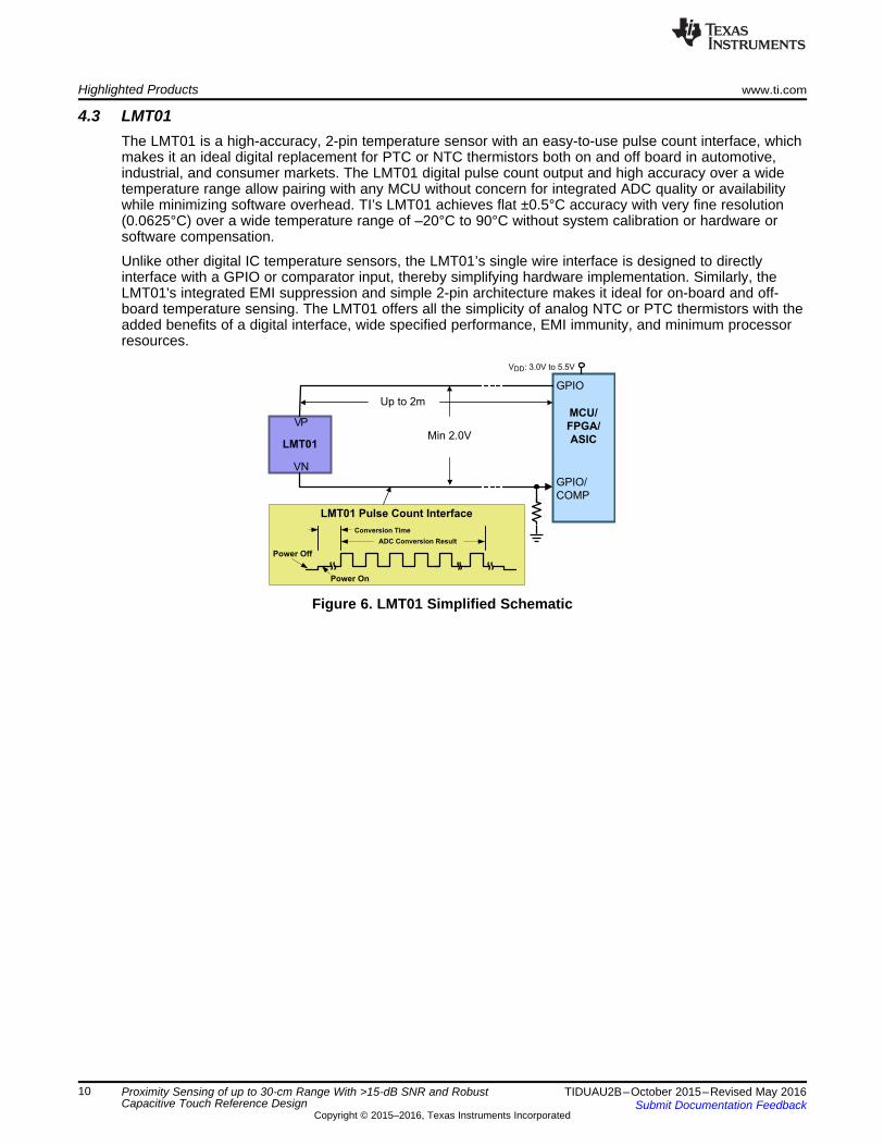
4.3 LMT01The LMT01 is a high-accuracy, 2-pin temperature sensor with an easy-to-use pulse count interface, whichmakes it an ideal digital replacement for PTC or NTC thermistors both on and off board in automotive,industrial, and consumer markets. The LMT01 digital pulse count output and high accuracy over a widetemperature range allow pairing with any MCU without concern for integrated ADC quality or availabilitywhile minimizing software overhead. TI’s LMT01 achieves flat ±0.5°C accuracy with very fine resolution(0.0625°C) over a wide temperature range of –20°C to 90°C without system calibration or hardware orsoftware compensation.
Unlike other digital IC temperature sensors, the LMT01’s single wire interface is designed to directlyinterface with a GPIO or comparator input, thereby simplifying hardware implementation. Similarly, theLMT01's integrated EMI suppression and simple 2-pin architecture makes it ideal for on-board and off-board temperature sensing. The LMT01 offers all the simplicity of analog NTC or PTC thermistors with theadded benefits of a digital interface, wide specified performance, EMI immunity, and minimum processorresources.
Figure 6. LMT01 Simplified Schematic
2
4
3
8
10VIN
TPS92513
PDIM
UVLO
COMP
PH
57
RT/CLKISENSE
6
IADJ
1
BOOT
9
GND
Pad
0.18V ± 1.8V
www.ti.com Highlighted Products
11TIDUAU2B–October 2015–Revised May 2016Submit Documentation Feedback
Copyright © 2015–2016, Texas Instruments Incorporated
Proximity Sensing of up to 30-cm Range With >15-dB SNR and RobustCapacitive Touch Reference Design
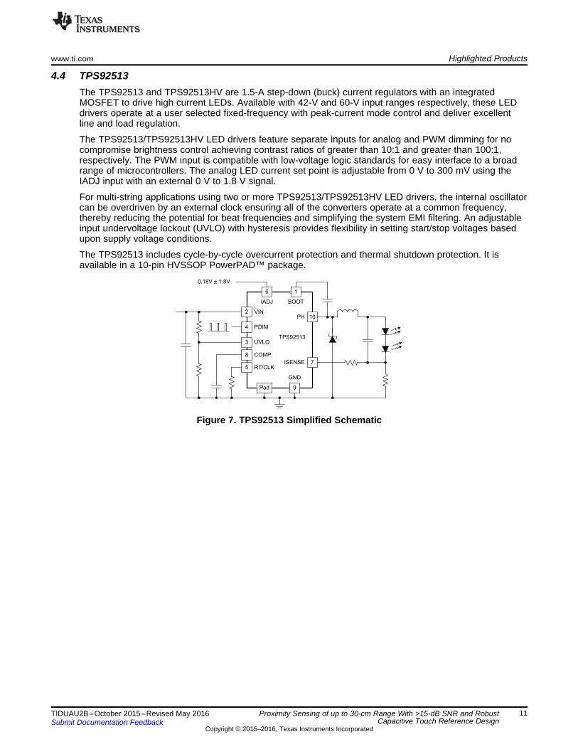
4.4 TPS92513The TPS92513 and TPS92513HV are 1.5-A step-down (buck) current regulators with an integratedMOSFET to drive high current LEDs. Available with 42-V and 60-V input ranges respectively, these LEDdrivers operate at a user selected fixed-frequency with peak-current mode control and deliver excellentline and load regulation.
The TPS92513/TPS92513HV LED drivers feature separate inputs for analog and PWM dimming for nocompromise brightness control achieving contrast ratios of greater than 10:1 and greater than 100:1,respectively. The PWM input is compatible with low-voltage logic standards for easy interface to a broadrange of microcontrollers. The analog LED current set point is adjustable from 0 V to 300 mV using theIADJ input with an external 0 V to 1.8 V signal.
For multi-string applications using two or more TPS92513/TPS92513HV LED drivers, the internal oscillatorcan be overdriven by an external clock ensuring all of the converters operate at a common frequency,thereby reducing the potential for beat frequencies and simplifying the system EMI filtering. An adjustableinput undervoltage lockout (UVLO) with hysteresis provides flexibility in setting start/stop voltages basedupon supply voltage conditions.
The TPS92513 includes cycle-by-cycle overcurrent protection and thermal shutdown protection. It isavailable in a 10-pin HVSSOP PowerPAD™ package.
Figure 7. TPS92513 Simplified Schematic
Clock
System
Brownout
Protection
RST/NMI
DVCC DVSS
MCLK
Watchdog
WDT+
15-Bit
Timer0_A3
3 CC
Registers
16MHz
CPU
incl. 16
Registers
Emulation
2BP
JTAG
Interface
SMCLK
ACLK
MDB
MAB
Port P1
8 I/O
Interrupt
capability
pullup/down
resistors
P1.x
8
P2.x
Port P2
8 I/O
Interrupt
capability
pullup/down
resistors
Spy-Bi-
Wire
Comp_A+
8 Channels
Timer1_A3
3 CC
Registers
XIN XOUT
Port P3
8 I/O
pullup/
pulldown
resistors
P3.x
8 8
RAM
512B
256B
Flash
16KB
8KB
4KB
2KB
USCI A0
UART/
LIN, IrDA,
SPI
USCI B0
SPI, I2C
ADC
10-Bit
8 Ch.
Autoscan
1 ch DMA
Highlighted Products www.ti.com
12 TIDUAU2B–October 2015–Revised May 2016Submit Documentation Feedback
Copyright © 2015–2016, Texas Instruments Incorporated
Proximity Sensing of up to 30-cm Range With >15-dB SNR and RobustCapacitive Touch Reference Design
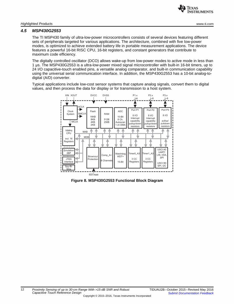
4.5 MSP430G2553The TI MSP430 family of ultra-low-power microcontrollers consists of several devices featuring differentsets of peripherals targeted for various applications. The architecture, combined with five low-powermodes, is optimized to achieve extended battery life in portable measurement applications. The devicefeatures a powerful 16-bit RISC CPU, 16-bit registers, and constant generators that contribute tomaximum code efficiency.
The digitally controlled oscillator (DCO) allows wake-up from low-power modes to active mode in less than1 μs. The MSP430G2553 is a ultra-low-power mixed signal microcontroller with built-in 16-bit timers, up to24 I/O capacitive-touch enabled pins, a versatile analog comparator, and built-in communication capabilityusing the universal serial communication interface. In addition, the MSP430G2553 has a 10-bit analog-to-digital (A/D) converter.
Typical applications include low-cost sensor systems that capture analog signals, convert them to digitalvalues, and then process the data for display or for transmission to a host system.
Figure 8. MSP430G2553 Functional Block Diagram
_+
Current
Sense
R1
R2
VIN
GND
VOUT
ILIM
Bandgap
Reference
VREF = 1.205 V
R = 840 kW2
www.ti.com Highlighted Products
13TIDUAU2B–October 2015–Revised May 2016Submit Documentation Feedback
Copyright © 2015–2016, Texas Instruments Incorporated
Proximity Sensing of up to 30-cm Range With >15-dB SNR and RobustCapacitive Touch Reference Design
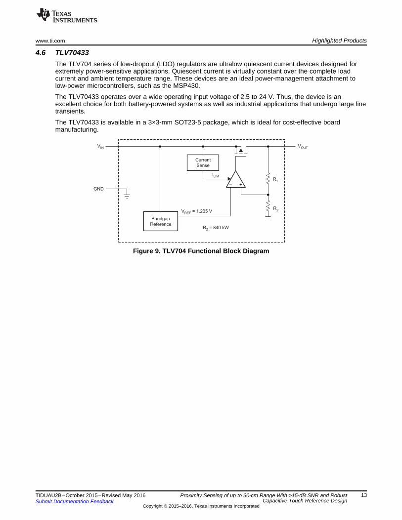
4.6 TLV70433The TLV704 series of low-dropout (LDO) regulators are ultralow quiescent current devices designed forextremely power-sensitive applications. Quiescent current is virtually constant over the complete loadcurrent and ambient temperature range. These devices are an ideal power-management attachment tolow-power microcontrollers, such as the MSP430.
The TLV70433 operates over a wide operating input voltage of 2.5 to 24 V. Thus, the device is anexcellent choice for both battery-powered systems as well as industrial applications that undergo large linetransients.
The TLV70433 is available in a 3×3-mm SOT23-5 package, which is ideal for cost-effective boardmanufacturing.
Figure 9. TLV704 Functional Block Diagram
3 5
4
GND
TPD2E2U06
US
B 2
.0
Tra
nsceiv
er
US
B 2
.0
Connecto
r D+
D-
GND
Vbus
Power
Supply
Highlighted Products www.ti.com
14 TIDUAU2B–October 2015–Revised May 2016Submit Documentation Feedback
Copyright © 2015–2016, Texas Instruments Incorporated
Proximity Sensing of up to 30-cm Range With >15-dB SNR and RobustCapacitive Touch Reference Design
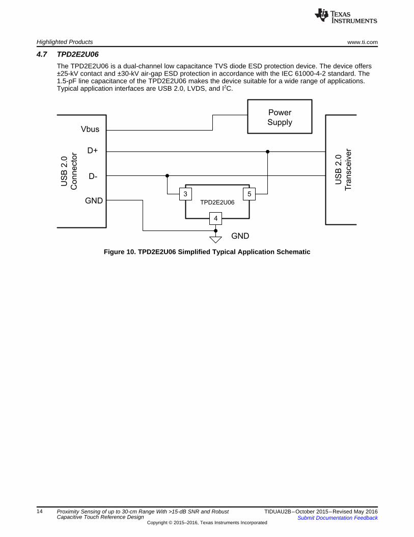
4.7 TPD2E2U06The TPD2E2U06 is a dual-channel low capacitance TVS diode ESD protection device. The device offers±25-kV contact and ±30-kV air-gap ESD protection in accordance with the IEC 61000-4-2 standard. The1.5-pF line capacitance of the TPD2E2U06 makes the device suitable for a wide range of applications.Typical application interfaces are USB 2.0, LVDS, and I2C.
Figure 10. TPD2E2U06 Simplified Typical Application Schematic
18µH
L15
1 234
L16DNP
18pF
C54DNP
33pF
C56
18pF
C57DNP GND
18pF
C55DNP
18pF
C58DNP GND
18µH
L17
1 234
L18DNP
18pF
C62DNP
33pF
C64
18pF
C65DNP GND
18pF
C63DNP
18pF
C66DNP GND
Header: Molex 43650-0313
Receptacle: 43645-0300
Terminal: 43030-0002
To proximity sensing
electrode sensors
TP30
TP28
TP24
TP21
NC1
NC2
IO13
GND4
IO25
U12
TPD2E2U06DRL
DNP
GND
IO Capacitance = 51pF
– ±8-kV IEC 61000-4-2Contact Discharge
– ±15-kV IEC 61000-4-2Air-Gap Discharge
1
2
3
J13
61300311121
1F
2 LC=
p
www.ti.com System Design Theory
15TIDUAU2B–October 2015–Revised May 2016Submit Documentation Feedback
Copyright © 2015–2016, Texas Instruments Incorporated
Proximity Sensing of up to 30-cm Range With >15-dB SNR and RobustCapacitive Touch Reference Design
5 System Design TheoryThis system is designed targeting the human machine interface application for cooker hood applications.
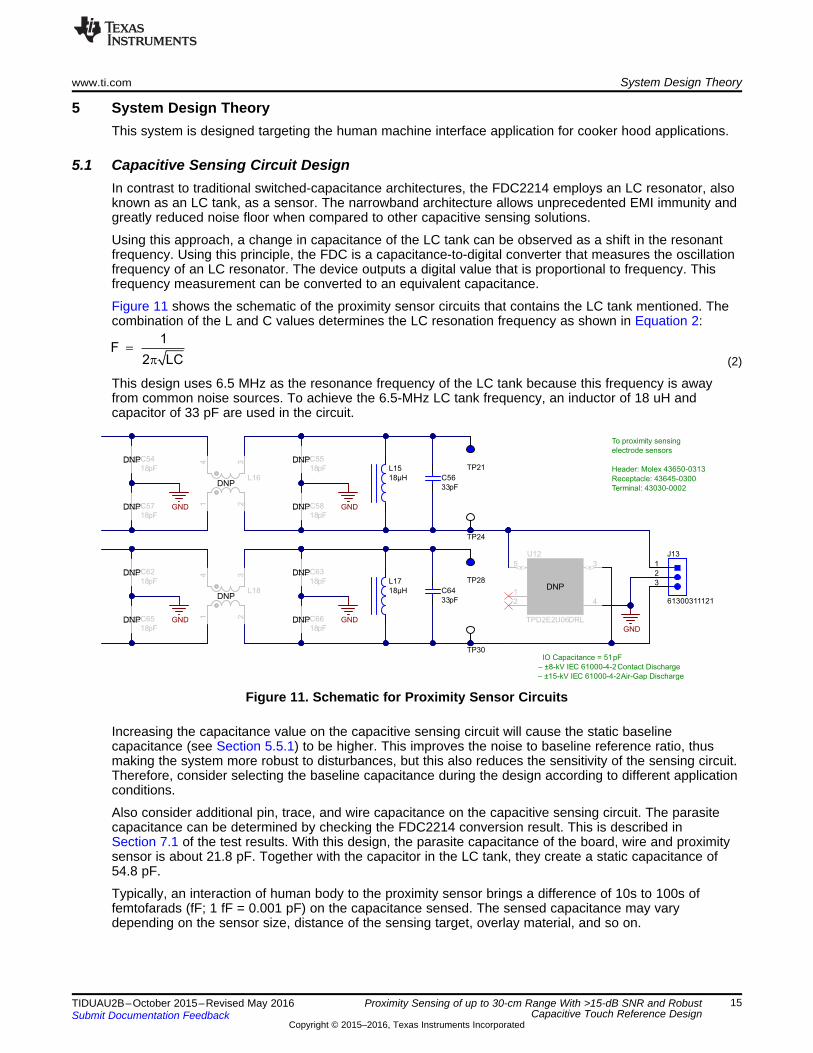
5.1 Capacitive Sensing Circuit DesignIn contrast to traditional switched-capacitance architectures, the FDC2214 employs an LC resonator, alsoknown as an LC tank, as a sensor. The narrowband architecture allows unprecedented EMI immunity andgreatly reduced noise floor when compared to other capacitive sensing solutions.
Using this approach, a change in capacitance of the LC tank can be observed as a shift in the resonantfrequency. Using this principle, the FDC is a capacitance-to-digital converter that measures the oscillationfrequency of an LC resonator. The device outputs a digital value that is proportional to frequency. Thisfrequency measurement can be converted to an equivalent capacitance.
Figure 11 shows the schematic of the proximity sensor circuits that contains the LC tank mentioned. Thecombination of the L and C values determines the LC resonation frequency as shown in Equation 2:
(2)
This design uses 6.5 MHz as the resonance frequency of the LC tank because this frequency is awayfrom common noise sources. To achieve the 6.5-MHz LC tank frequency, an inductor of 18 uH andcapacitor of 33 pF are used in the circuit.
Figure 11. Schematic for Proximity Sensor Circuits
Increasing the capacitance value on the capacitive sensing circuit will cause the static baselinecapacitance (see Section 5.5.1) to be higher. This improves the noise to baseline reference ratio, thusmaking the system more robust to disturbances, but this also reduces the sensitivity of the sensing circuit.Therefore, consider selecting the baseline capacitance during the design according to different applicationconditions.
Also consider additional pin, trace, and wire capacitance on the capacitive sensing circuit. The parasitecapacitance can be determined by checking the FDC2214 conversion result. This is described inSection 7.1 of the test results. With this design, the parasite capacitance of the board, wire and proximitysensor is about 21.8 pF. Together with the capacitor in the LC tank, they create a static capacitance of54.8 pF.
Typically, an interaction of human body to the proximity sensor brings a difference of 10s to 100s offemtofarads (fF; 1 fF = 0.001 pF) on the capacitance sensed. The sensed capacitance may varydepending on the sensor size, distance of the sensing target, overlay material, and so on.
REFSENSOR 28
CH_FIN_ SEL f Countf
2
´ ´
=
( )SENSOR 2
SENSOR
1C C
L 2 f
= -
´ p ´
System Design Theory www.ti.com
16 TIDUAU2B–October 2015–Revised May 2016Submit Documentation Feedback
Copyright © 2015–2016, Texas Instruments Incorporated
Proximity Sensing of up to 30-cm Range With >15-dB SNR and RobustCapacitive Touch Reference Design
Therefore, one of the design challenges for proximity sensing is the ratio between the capacitance sensedand the static capacitance of the system. Minimizing the static capacitance of the system is one of themost commonly considered solutions, but it is difficult to achieve due to the nature of the electroniccomponents, the wire, and, sometimes, the frame of the end equipment.
The FDC2214 addresses this problem very nicely with 28 bits of high resolution conversion results,providing an accurate reading on small changes of the sensed capacitance.
The conversion value of the FDC2214 can be translated into capacitance by Equation 3:
(3)
Where:• C is the parallel sensor capacitance (capacitance of the LC tank).
fSENSOR is calculated by Equation 4:
(4)
Where:• CH_FIN_SEL is the "sensor frequency select" bit value in FDC2214 register, which is 1 in this design• fREF is the reference frequency of the channel which is 40 MHz in this design
With the equations above, translate the conversion result into capacitance. For example, if the conversionresult is 36716045 (0x2303E0D) counts, the sensed capacitance on the sensor is 14.013 pF.
Do not populate (DNP) components in the schematic shown in Figure 11 are the optional components toenhance noise filtering when the circuit is to be used under harsh environment conditions (see SNOU138for more information).
www.ti.com System Design Theory
17TIDUAU2B–October 2015–Revised May 2016Submit Documentation Feedback
Copyright © 2015–2016, Texas Instruments Incorporated
Proximity Sensing of up to 30-cm Range With >15-dB SNR and RobustCapacitive Touch Reference Design
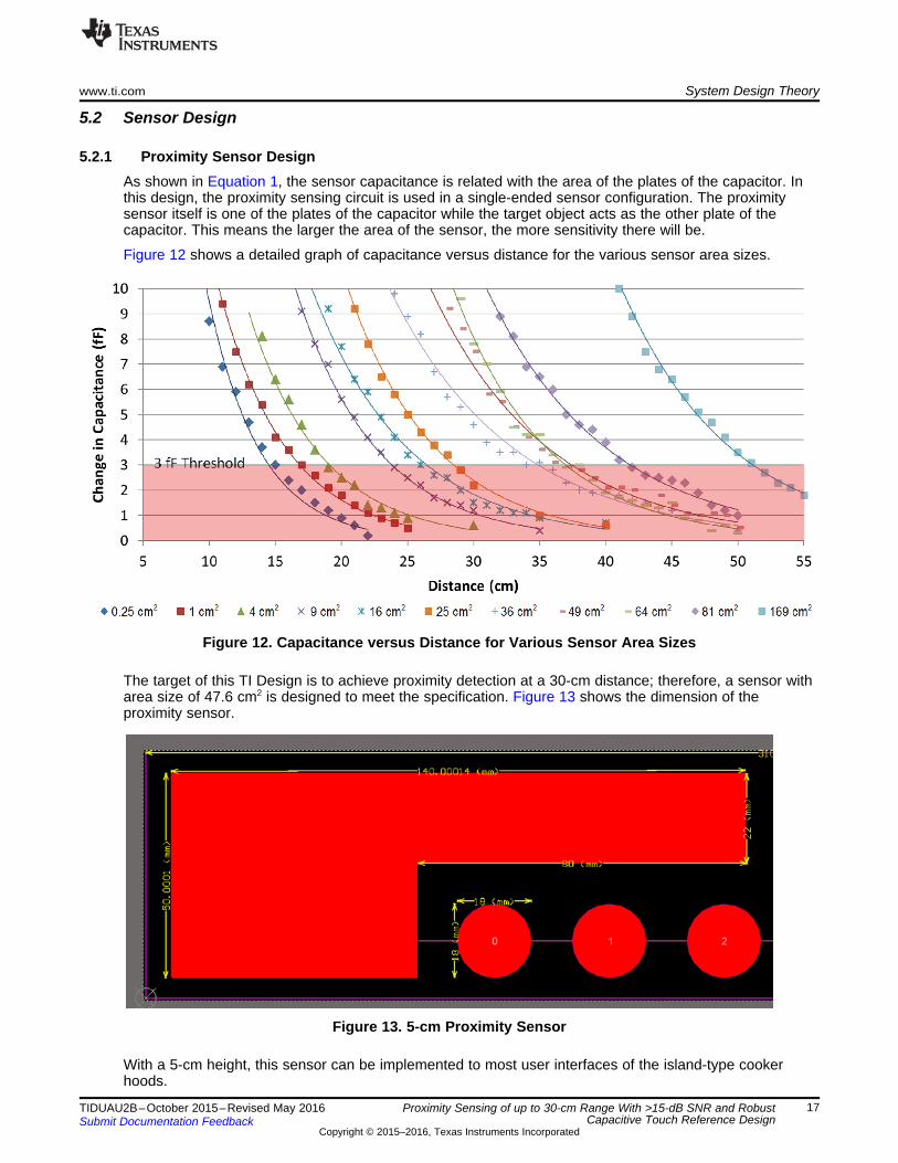
5.2 Sensor Design
5.2.1 Proximity Sensor DesignAs shown in Equation 1, the sensor capacitance is related with the area of the plates of the capacitor. Inthis design, the proximity sensing circuit is used in a single-ended sensor configuration. The proximitysensor itself is one of the plates of the capacitor while the target object acts as the other plate of thecapacitor. This means the larger the area of the sensor, the more sensitivity there will be.
Figure 12 shows a detailed graph of capacitance versus distance for the various sensor area sizes.
Figure 12. Capacitance versus Distance for Various Sensor Area Sizes
The target of this TI Design is to achieve proximity detection at a 30-cm distance; therefore, a sensor witharea size of 47.6 cm2 is designed to meet the specification. Figure 13 shows the dimension of theproximity sensor.
Figure 13. 5-cm Proximity Sensor
With a 5-cm height, this sensor can be implemented to most user interfaces of the island-type cookerhoods.
System Design Theory www.ti.com
18 TIDUAU2B–October 2015–Revised May 2016Submit Documentation Feedback
Copyright © 2015–2016, Texas Instruments Incorporated
Proximity Sensing of up to 30-cm Range With >15-dB SNR and RobustCapacitive Touch Reference Design
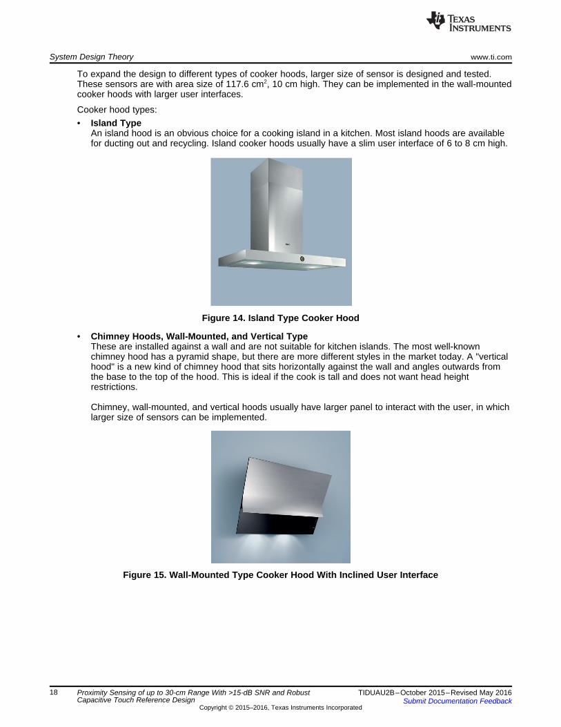
To expand the design to different types of cooker hoods, larger size of sensor is designed and tested.These sensors are with area size of 117.6 cm2, 10 cm high. They can be implemented in the wall-mountedcooker hoods with larger user interfaces.
Cooker hood types:• Island Type
An island hood is an obvious choice for a cooking island in a kitchen. Most island hoods are availablefor ducting out and recycling. Island cooker hoods usually have a slim user interface of 6 to 8 cm high.
Figure 14. Island Type Cooker Hood
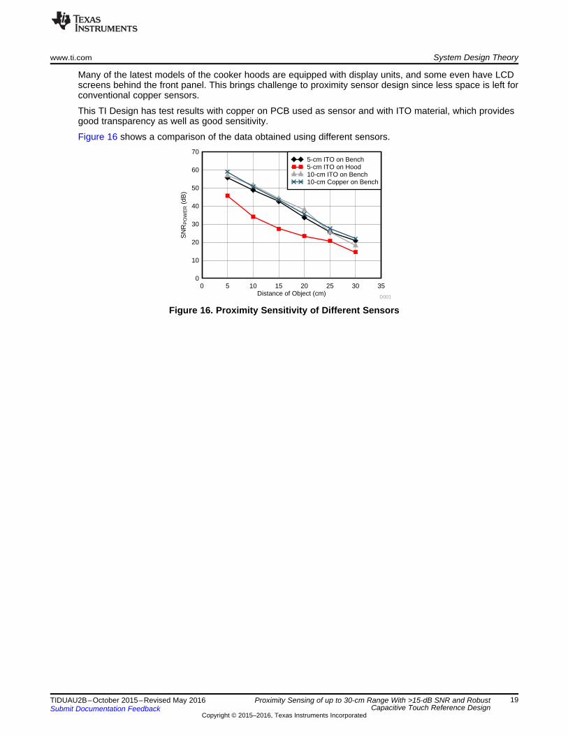
• Chimney Hoods, Wall-Mounted, and Vertical TypeThese are installed against a wall and are not suitable for kitchen islands. The most well-knownchimney hood has a pyramid shape, but there are more different styles in the market today. A "verticalhood" is a new kind of chimney hood that sits horizontally against the wall and angles outwards fromthe base to the top of the hood. This is ideal if the cook is tall and does not want head heightrestrictions.spaceChimney, wall-mounted, and vertical hoods usually have larger panel to interact with the user, in whichlarger size of sensors can be implemented.
Figure 15. Wall-Mounted Type Cooker Hood With Inclined User Interface
Distance of Object (cm)
SN
RP
OW
ER (
dB)
0 5 10 15 20 25 30 350
10
20
30
40
50
60
70
D001
5-cm ITO on Bench5-cm ITO on Hood10-cm ITO on Bench10-cm Copper on Bench
www.ti.com System Design Theory
19TIDUAU2B–October 2015–Revised May 2016Submit Documentation Feedback
Copyright © 2015–2016, Texas Instruments Incorporated
Proximity Sensing of up to 30-cm Range With >15-dB SNR and RobustCapacitive Touch Reference Design
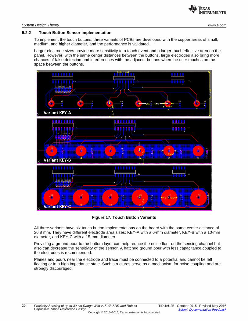
Many of the latest models of the cooker hoods are equipped with display units, and some even have LCDscreens behind the front panel. This brings challenge to proximity sensor design since less space is left forconventional copper sensors.
This TI Design has test results with copper on PCB used as sensor and with ITO material, which providesgood transparency as well as good sensitivity.
Figure 16 shows a comparison of the data obtained using different sensors.
Figure 16. Proximity Sensitivity of Different Sensors
System Design Theory www.ti.com
20 TIDUAU2B–October 2015–Revised May 2016Submit Documentation Feedback
Copyright © 2015–2016, Texas Instruments Incorporated
Proximity Sensing of up to 30-cm Range With >15-dB SNR and RobustCapacitive Touch Reference Design
5.2.2 Touch Button Sensor ImplementationTo implement the touch buttons, three variants of PCBs are developed with the copper areas of small,medium, and higher diameter, and the performance is validated.
Larger electrode sizes provide more sensitivity to a touch event and a larger touch effective area on thepanel. However, with the same center distances between the buttons, large electrodes also bring morechances of false detection and interferences with the adjacent buttons when the user touches on thespace between the buttons.
Figure 17. Touch Button Variants
All three variants have six touch button implementations on the board with the same center distance of26.8 mm. They have different electrode area sizes: KEY-A with a 6-mm diameter, KEY-B with a 10-mmdiameter, and KEY-C with a 15-mm diameter.
Providing a ground pour to the bottom layer can help reduce the noise floor on the sensing channel butalso can decrease the sensitivity of the sensor. A hatched ground pour with less capacitance coupled tothe electrodes is recommended.
Planes and pours near the electrode and trace must be connected to a potential and cannot be leftfloating or in a high impedance state. Such structures serve as a mechanism for noise coupling and arestrongly discouraged.
15 mm 5 mm10 mmsmallmedium
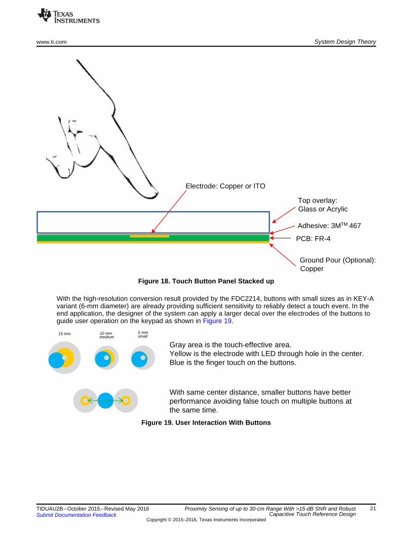
Gray area is the touch-effective area.Yellow is the electrode with LED through hole in the center.Blue is the finger touch on the buttons.
With same center distance, smaller buttons have better performance avoiding false touch on multiple buttons at the same time.
Top overlay: Glass or Acrylic
Adhesive: 3MTM 467
Electrode: Copper or ITO
Ground Pour (Optional): Copper
PCB: FR-4
www.ti.com System Design Theory
21TIDUAU2B–October 2015–Revised May 2016Submit Documentation Feedback
Copyright © 2015–2016, Texas Instruments Incorporated
Proximity Sensing of up to 30-cm Range With >15-dB SNR and RobustCapacitive Touch Reference Design
Figure 18. Touch Button Panel Stacked up
With the high-resolution conversion result provided by the FDC2214, buttons with small sizes as in KEY-Avariant (6-mm diameter) are already providing sufficient sensitivity to reliably detect a touch event. In theend application, the designer of the system can apply a larger decal over the electrodes of the buttons toguide user operation on the keypad as shown in Figure 19.
Figure 19. User Interaction With Buttons
System Design Theory www.ti.com
22 TIDUAU2B–October 2015–Revised May 2016Submit Documentation Feedback
Copyright © 2015–2016, Texas Instruments Incorporated
Proximity Sensing of up to 30-cm Range With >15-dB SNR and RobustCapacitive Touch Reference Design
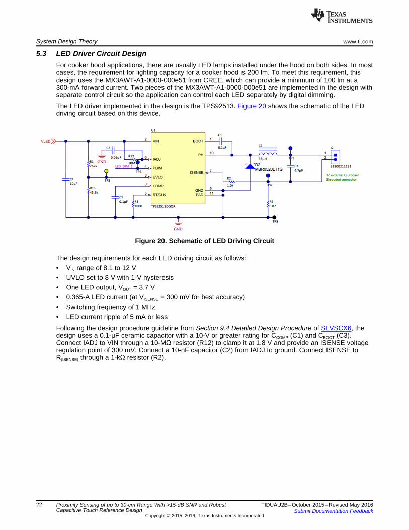
5.3 LED Driver Circuit DesignFor cooker hood applications, there are usually LED lamps installed under the hood on both sides. In mostcases, the requirement for lighting capacity for a cooker hood is 200 lm. To meet this requirement, thisdesign uses the MX3AWT-A1-0000-000e51 from CREE, which can provide a minimum of 100 lm at a300-mA forward current. Two pieces of the MX3AWT-A1-0000-000e51 are implemented in the design withseparate control circuit so the application can control each LED separately by digital dimming.
The LED driver implemented in the design is the TPS92513. Figure 20 shows the schematic of the LEDdriving circuit based on this device.
Figure 20. Schematic of LED Driving Circuit
The design requirements for each LED driving circuit as follows:• VIN range of 8.1 to 12 V• UVLO set to 8 V with 1-V hysteresis• One LED output, VOUT = 3.7 V• 0.365-A LED current (at VISENSE = 300 mV for best accuracy)• Switching frequency of 1 MHz• LED current ripple of 5 mA or less
Following the design procedure guideline from Section 9.4 Detailed Design Procedure of SLVSCX6, thedesign uses a 0.1-μF ceramic capacitor with a 10-V or greater rating for CCOMP (C1) and CBOOT (C3).Connect IADJ to VIN through a 10-MΩ resistor (R12) to clamp it at 1.8 V and provide an ISENSE voltageregulation point of 300 mV. Connect a 10-nF capacitor (C2) from IADJ to ground. Connect ISENSE toR(ISENSE) through a 1-kΩ resistor (R2).
DIODE D _ AVE FP I V 242.79 mA 0.7 V 170 mW= ´ = ´ =
( ) ( )D _ AVE LEDI I 1 Duty 365.85 mA 1 – 33.6% 242.79 mA= ´ - = ´ =
( )OUT IN OUT
R IN SW
V V VL
I V f
´ -=
´ ´
ISENSE
300 mVR 0.822
0.365 A= = W
( )( )
( )RT 1.092
20633R K 109.13 K
1000
W = = W
( )( )( ) ( ) ( )
EN ESD HYS
STOP EN HYS ESD
R1 V R I1 I
R2V V I1 I R1 R
é ù´ - ´ +ë û=
- + + ´ +
( )HYS EN ESD HYS ESD START
HYS EN
V V I1 R I R V
R1I V
é ù´ - ´ - ´ ´ë û=´
www.ti.com System Design Theory
23TIDUAU2B–October 2015–Revised May 2016Submit Documentation Feedback
Copyright © 2015–2016, Texas Instruments Incorporated
Proximity Sensing of up to 30-cm Range With >15-dB SNR and RobustCapacitive Touch Reference Design
Calculate UVLO resistor valueUse the following equations to determine the values of R1 and R15.
(5)
(6)
Where:• VHYS = VSTART – VSTOP = 1 V• RESD = 10 KΩ• VEN = 1.22 V• IHYS = 2.9 µA
This results in R1 = 268.23 KΩ, R15 = 45.77 KΩ, and in the hardware implementation, the design usesR1 = 267 KΩ and R15 = 45.9 KΩ.
Calculate RT resistor (R3) value
(7)
The design uses a 100-KΩ resistor, which results in a 1.083-MHz switching frequency in theory.
Calculate ISENSE resistor (R4)
(8)
The design uses a 0.82-Ω resistor with a 0.5-W power level.
Calculate inductor value (L1)According to Equation 9, the inductor value can be determined:
(9)
Where:• VOUT = 4.07 V (3.7 V with a 10% margin)• VIN = 8.1 V (9 V with a -10% margin)• IR = 75 mA (as recommended by datasheet)• fSW = 1.083 MHz
The inductance results in 24.9 µH, with IRMS = 0.366 A and IPEAK = 0.403 A, LPS5015-333MR is selectedwith 33 µH and ISAT with 30% drop at 0.6 A, IRMS of 0.7 A with 40°C rise.
Following the design procedure, select a 10-µF/50-V input capacitor as CIN (C4) and 4.7-µF/16-V outputcapacitor as COUT (C3).
Calculate the diode power dissipation (D)According to the calculation above, the average current on the output diode is:
(10)
(11)
MBR0520LT1G with average forward current of 0.5 A is a good fit for the hardware implementation.
SCL1
SDA2
CLKIN3
ADDR4
INTB5
SD6
VDD7
GND8
IN0A9
IN0B10
IN1A11
IN1B12
PAD17
IN2A13
IN2B14
IN3A15
IN3B16
U7
FDC2214RGHR
1µF
C59
GND
VCC
GND
GND
Address = 0x2A
S1_INT
S1_SHUTDOWN
Cap Sensor 1
S1_CLKIN
TP22
TP25
0.1µF
C60
0.01µF
C61
System Design Theory www.ti.com
24 TIDUAU2B–October 2015–Revised May 2016Submit Documentation Feedback
Copyright © 2015–2016, Texas Instruments Incorporated
Proximity Sensing of up to 30-cm Range With >15-dB SNR and RobustCapacitive Touch Reference Design
5.4 Control of Key ComponentsThe key components in this design are the sensor devices of the FDC2214, HDC1050, and LMT01. Thissection covers how to control these devices from the MCU and user application.
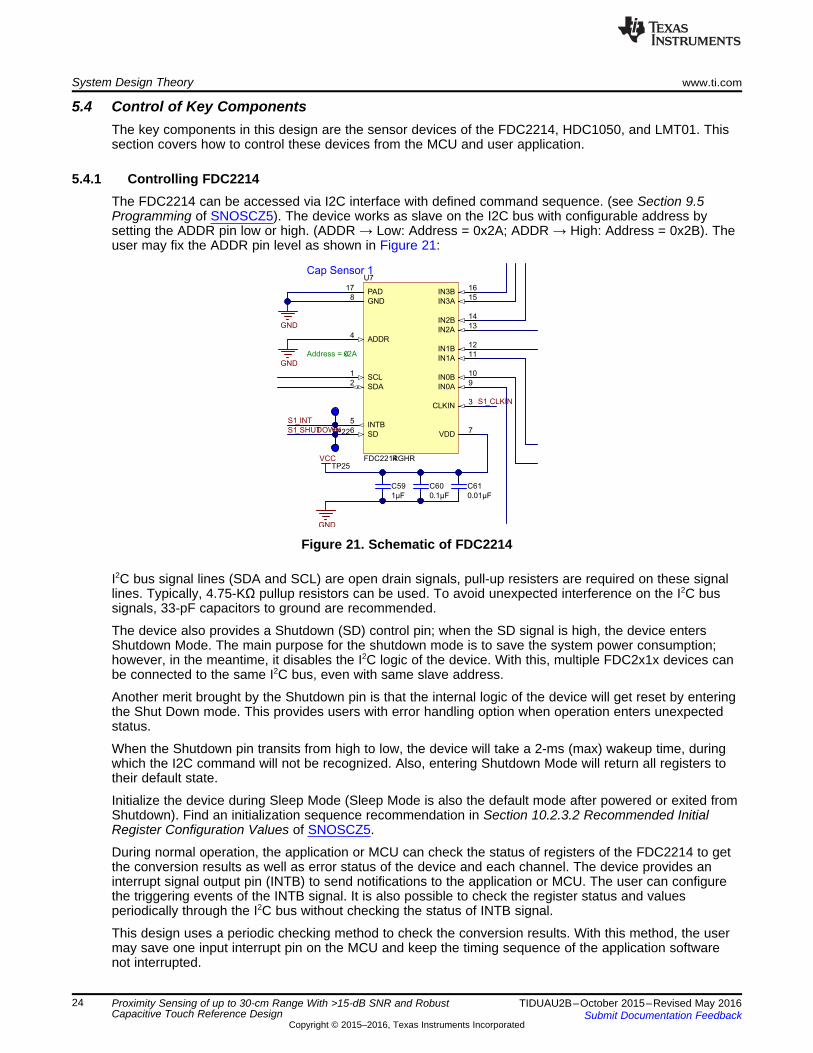
5.4.1 Controlling FDC2214The FDC2214 can be accessed via I2C interface with defined command sequence. (see Section 9.5Programming of SNOSCZ5). The device works as slave on the I2C bus with configurable address bysetting the ADDR pin low or high. (ADDR → Low: Address = 0x2A; ADDR → High: Address = 0x2B). Theuser may fix the ADDR pin level as shown in Figure 21:
Figure 21. Schematic of FDC2214
I2C bus signal lines (SDA and SCL) are open drain signals, pull-up resisters are required on these signallines. Typically, 4.75-KΩ pullup resistors can be used. To avoid unexpected interference on the I2C bussignals, 33-pF capacitors to ground are recommended.
The device also provides a Shutdown (SD) control pin; when the SD signal is high, the device entersShutdown Mode. The main purpose for the shutdown mode is to save the system power consumption;however, in the meantime, it disables the I2C logic of the device. With this, multiple FDC2x1x devices canbe connected to the same I2C bus, even with same slave address.
Another merit brought by the Shutdown pin is that the internal logic of the device will get reset by enteringthe Shut Down mode. This provides users with error handling option when operation enters unexpectedstatus.
When the Shutdown pin transits from high to low, the device will take a 2-ms (max) wakeup time, duringwhich the I2C command will not be recognized. Also, entering Shutdown Mode will return all registers totheir default state.
Initialize the device during Sleep Mode (Sleep Mode is also the default mode after powered or exited fromShutdown). Find an initialization sequence recommendation in Section 10.2.3.2 Recommended InitialRegister Configuration Values of SNOSCZ5.
During normal operation, the application or MCU can check the status of registers of the FDC2214 to getthe conversion results as well as error status of the device and each channel. The device provides aninterrupt signal output pin (INTB) to send notifications to the application or MCU. The user can configurethe triggering events of the INTB signal. It is also possible to check the register status and valuesperiodically through the I2C bus without checking the status of INTB signal.
This design uses a periodic checking method to check the conversion results. With this method, the usermay save one input interrupt pin on the MCU and keep the timing sequence of the application softwarenot interrupted.
VCC4
E/D1
GND2
OUT3
40 MHz
Y2
625L3C040M00000
GND
VCC
GND
S1_CLKIN
S2_CLKIN
33.0
R38
33.0
R39
TP29
TP31
0.01µF
C67
nOSC_EN
Set FDC software driver to ³LQLWLDOL]LQJ´�PRGH
Set SD low to enableFDC operation
Initialize FDC control variables
FDC initializing
FDC working FDC stops
Waking up
Setting applied
Any error orpower save
Re-initialize
www.ti.com System Design Theory
25TIDUAU2B–October 2015–Revised May 2016Submit Documentation Feedback
Copyright © 2015–2016, Texas Instruments Incorporated
Proximity Sensing of up to 30-cm Range With >15-dB SNR and RobustCapacitive Touch Reference Design
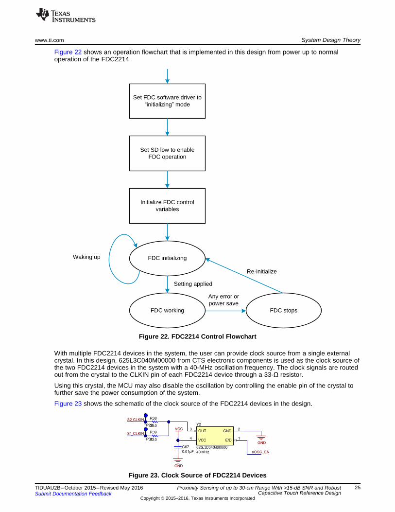
Figure 22 shows an operation flowchart that is implemented in this design from power up to normaloperation of the FDC2214.
Figure 22. FDC2214 Control Flowchart
With multiple FDC2214 devices in the system, the user can provide clock source from a single externalcrystal. In this design, 625L3C040M00000 from CTS electronic components is used as the clock source ofthe two FDC2214 devices in the system with a 40-MHz oscillation frequency. The clock signals are routedout from the crystal to the CLKIN pin of each FDC2214 device through a 33-Ω resistor.
Using this crystal, the MCU may also disable the oscillation by controlling the enable pin of the crystal tofurther save the power consumption of the system.
Figure 23 shows the schematic of the clock source of the FDC2214 devices in the design.
Figure 23. Clock Source of FDC2214 Devices
Initialize HDC configuration register
Trigger conversion
HDC sleep
HDC converting HDC error
Conversion finished
Re-initialize
Time to wake up
SDA1
GND2
NC3
NC4
VDD5
SCL6
PAD7
U6
HDC1050DMB
VCC
0.1µF
C48
GND
4
123
J15
61300411121
VCC
GND
Humidity Sensor
(Off board)
System Design Theory www.ti.com
26 TIDUAU2B–October 2015–Revised May 2016Submit Documentation Feedback
Copyright © 2015–2016, Texas Instruments Incorporated
Proximity Sensing of up to 30-cm Range With >15-dB SNR and RobustCapacitive Touch Reference Design
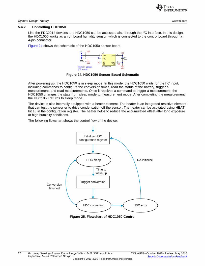
5.4.2 Controlling HDC1050Like the FDC2214 devices, the HDC1050 can be accessed also through the I2C interface. In this design,the HDC1050 works as an off board humidity sensor, which is connected to the control board through a4-pin connector.
Figure 24 shows the schematic of the HDC1050 sensor board.
Figure 24. HDC1050 Sensor Board Schematic
After powering up, the HDC1050 is in sleep mode. In this mode, the HDC1050 waits for the I2C input,including commands to configure the conversion times, read the status of the battery, trigger ameasurement, and read measurements. Once it receives a command to trigger a measurement, theHDC1050 changes the state from sleep mode to measurement mode. After completing the measurement,the HDC1050 returns to sleep mode.
The device is also internally equipped with a heater element. The heater is an integrated resistive elementthat can test the sensor or to drive condensation off the sensor. The heater can be activated using HEAT,bit 13 in the configuration register. The heater helps to reduce the accumulated offset after long exposureat high humidity conditions.
The following flowchart shows the control flow of the device:
Figure 25. Flowchart of HDC1050 Control
PCTemp 256 C 50 C
4096
æ ö= ´ ° - °ç ÷
è ø
1
2
J14
61300211121
TEMP_VP
To external LMT01
Shrouded connector
112.5 uA to 143uA current - 1.125 V to
1.43V on comparator input.
Comparator Vref = 0.25Vcc = 0.825VTP2610.0k
R33
GND
TEMP_IN
www.ti.com System Design Theory
27TIDUAU2B–October 2015–Revised May 2016Submit Documentation Feedback
Copyright © 2015–2016, Texas Instruments Incorporated
Proximity Sensing of up to 30-cm Range With >15-dB SNR and RobustCapacitive Touch Reference Design
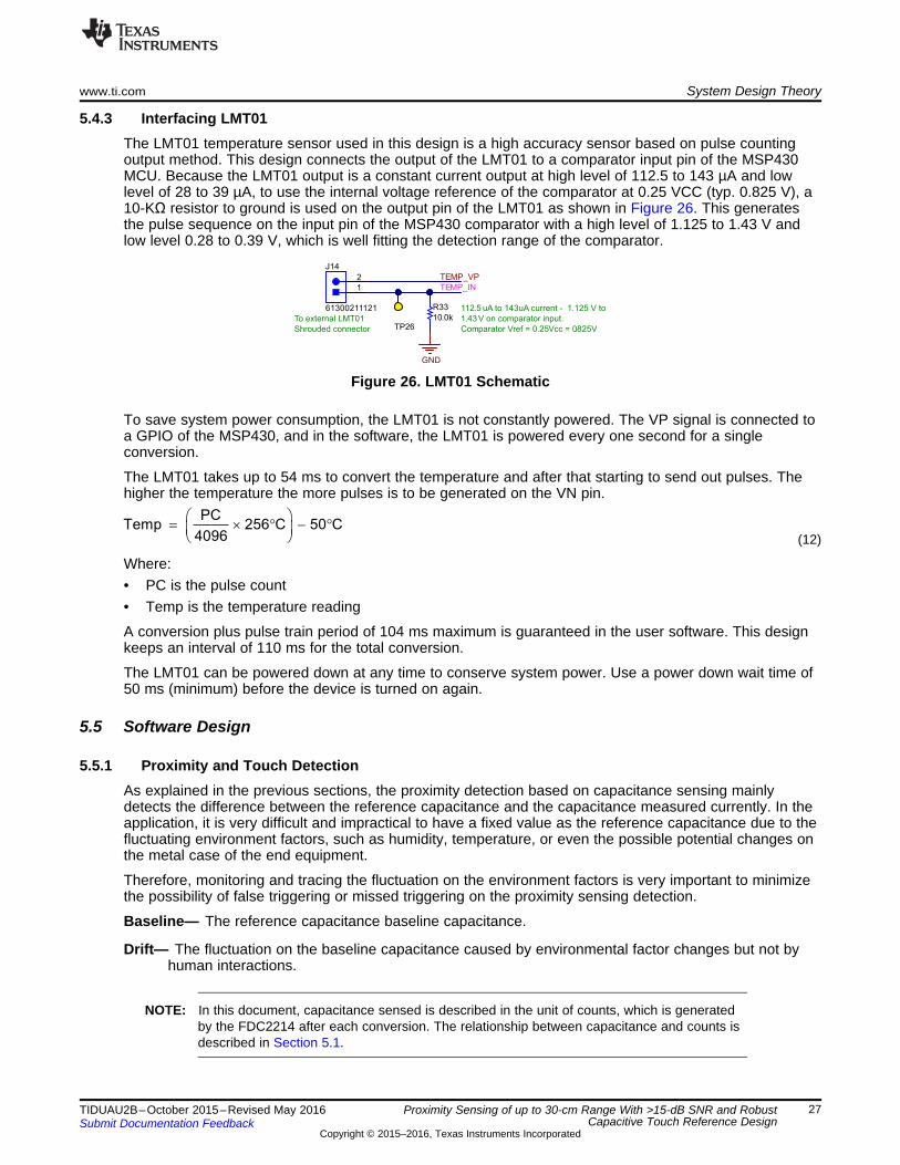
5.4.3 Interfacing LMT01The LMT01 temperature sensor used in this design is a high accuracy sensor based on pulse countingoutput method. This design connects the output of the LMT01 to a comparator input pin of the MSP430MCU. Because the LMT01 output is a constant current output at high level of 112.5 to 143 µA and lowlevel of 28 to 39 µA, to use the internal voltage reference of the comparator at 0.25 VCC (typ. 0.825 V), a10-KΩ resistor to ground is used on the output pin of the LMT01 as shown in Figure 26. This generatesthe pulse sequence on the input pin of the MSP430 comparator with a high level of 1.125 to 1.43 V andlow level 0.28 to 0.39 V, which is well fitting the detection range of the comparator.
Figure 26. LMT01 Schematic
To save system power consumption, the LMT01 is not constantly powered. The VP signal is connected toa GPIO of the MSP430, and in the software, the LMT01 is powered every one second for a singleconversion.
The LMT01 takes up to 54 ms to convert the temperature and after that starting to send out pulses. Thehigher the temperature the more pulses is to be generated on the VN pin.
(12)
Where:• PC is the pulse count• Temp is the temperature reading
A conversion plus pulse train period of 104 ms maximum is guaranteed in the user software. This designkeeps an interval of 110 ms for the total conversion.
The LMT01 can be powered down at any time to conserve system power. Use a power down wait time of50 ms (minimum) before the device is turned on again.
5.5 Software Design
5.5.1 Proximity and Touch DetectionAs explained in the previous sections, the proximity detection based on capacitance sensing mainlydetects the difference between the reference capacitance and the capacitance measured currently. In theapplication, it is very difficult and impractical to have a fixed value as the reference capacitance due to thefluctuating environment factors, such as humidity, temperature, or even the possible potential changes onthe metal case of the end equipment.
Therefore, monitoring and tracing the fluctuation on the environment factors is very important to minimizethe possibility of false triggering or missed triggering on the proximity sensing detection.
Baseline— The reference capacitance baseline capacitance.
Drift— The fluctuation on the baseline capacitance caused by environmental factor changes but not byhuman interactions.
NOTE: In this document, capacitance sensed is described in the unit of counts, which is generatedby the FDC2214 after each conversion. The relationship between capacitance and counts isdescribed in Section 5.1.
Sum
First-order filter CompareReadingCount
Baseline
Proximity level
Threshold
On/Off1í
ZFirst-order filterReading
Proximity event
Delay unit
Baseline value
System Design Theory www.ti.com
28 TIDUAU2B–October 2015–Revised May 2016Submit Documentation Feedback
Copyright © 2015–2016, Texas Instruments Incorporated
Proximity Sensing of up to 30-cm Range With >15-dB SNR and RobustCapacitive Touch Reference Design
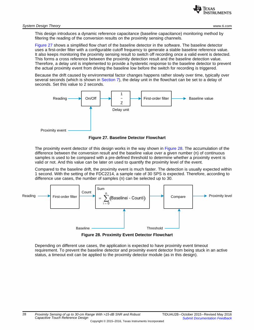
This design introduces a dynamic reference capacitance (baseline capacitance) monitoring method byfiltering the reading of the conversion results on the proximity sensing channels.
Figure 27 shows a simplified flow chart of the baseline detector in the software. The baseline detectoruses a first-order filter with a configurable cutoff frequency to generate a stable baseline reference value.It also keeps monitoring the proximity sensing result to switch off recording once a valid event is detected.This forms a cross reference between the proximity detection result and the baseline detection value.Therefore, a delay unit is implemented to provide a hysteretic response to the baseline detector to preventthe actual proximity event from driving the baseline low before the switch for recording is triggered.
Because the drift caused by environmental factor changes happens rather slowly over time, typically overseveral seconds (which is shown in Section 7), the delay unit in the flowchart can be set to a delay ofseconds. Set this value to 2 seconds.
Figure 27. Baseline Detector Flowchart
The proximity event detector of this design works in the way shown in Figure 28. The accumulation of thedifference between the conversion result and the baseline value over a given number (n) of continuoussamples is used to be compared with a pre-defined threshold to determine whether a proximity event isvalid or not. And this value can be later on used to quantify the proximity level of the event.
Compared to the baseline drift, the proximity event is much faster. The detection is usually expected within1 second. With the setting of the FDC2214, a sample rate of 30 SPS is expected. Therefore, according todifference use cases, the number of samples (n) can be selected up to 30.
Figure 28. Proximity Event Detector Flowchart
Depending on different use cases, the application is expected to have proximity event timeoutrequirement. To prevent the baseline detector and proximity event detector from being stuck in an activestatus, a timeout exit can be applied to the proximity detector module (as in this design).
CSENSE í�CBASE > KeyTH?
CSENSE í�CBASE > Adjacent keys?
Filter samples to avoid glitch
Press detected
No pressNo
No
No glitch
Yes
Yes
www.ti.com System Design Theory
29TIDUAU2B–October 2015–Revised May 2016Submit Documentation Feedback
Copyright © 2015–2016, Texas Instruments Incorporated
Proximity Sensing of up to 30-cm Range With >15-dB SNR and RobustCapacitive Touch Reference Design
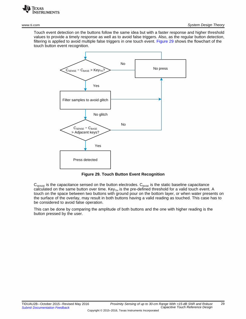
Touch event detection on the buttons follow the same idea but with a faster response and higher thresholdvalues to provide a timely response as well as to avoid false triggers. Also, as the regular button detection,filtering is applied to avoid multiple false triggers in one touch event. Figure 29 shows the flowchart of thetouch button event recognition.
Figure 29. Touch Button Event Recognition
CSENSE is the capacitance sensed on the button electrodes. CBASE is the static baseline capacitancecalculated on the same button over time. KeyTH is the pre-defined threshold for a valid touch event. Atouch on the space between two buttons with ground pour on the bottom layer, or when water presents onthe surface of the overlay, may result in both buttons having a valid reading as touched. This case has tobe considered to avoid false operation.
This can be done by comparing the amplitude of both buttons and the one with higher reading is thebutton pressed by the user.
Time
Counts
0 2 4 6 8 10 12
0
20
40
60
80
100
120
D002
A
B
DTH
tTH
tout
tover
System Design Theory www.ti.com
30 TIDUAU2B–October 2015–Revised May 2016Submit Documentation Feedback
Copyright © 2015–2016, Texas Instruments Incorporated
Proximity Sensing of up to 30-cm Range With >15-dB SNR and RobustCapacitive Touch Reference Design
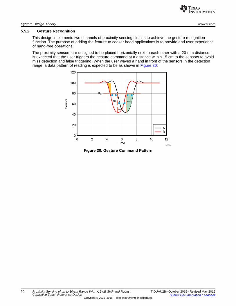
5.5.2 Gesture RecognitionThis design implements two channels of proximity sensing circuits to achieve the gesture recognitionfunction. The purpose of adding the feature to cooker hood applications is to provide end user experienceof hand-free operations.
The proximity sensors are designed to be placed horizontally next to each other with a 20-mm distance. Itis expected that the user triggers the gesture command at a distance within 15 cm to the sensors to avoidmiss detection and false triggering. When the user waves a hand in front of the sensors in the detectionrange, a data pattern of reading is expected to be as shown in Figure 30:
Figure 30. Gesture Command Pattern
[Pb > DTH]&&[Pa < DTH]
[Pb > DTH]&&[Pa < DTH]within tTH
[Pb > DTH]&&[Pa < DTH]within tOUT
[Pa < DTH]for longer than tOVER
Gesture command recognized
No gesture command Quit
Yes
Yes
Yes
Yes
Yes
No
No
No
No
www.ti.com System Design Theory
31TIDUAU2B–October 2015–Revised May 2016Submit Documentation Feedback
Copyright © 2015–2016, Texas Instruments Incorporated
Proximity Sensing of up to 30-cm Range With >15-dB SNR and RobustCapacitive Touch Reference Design
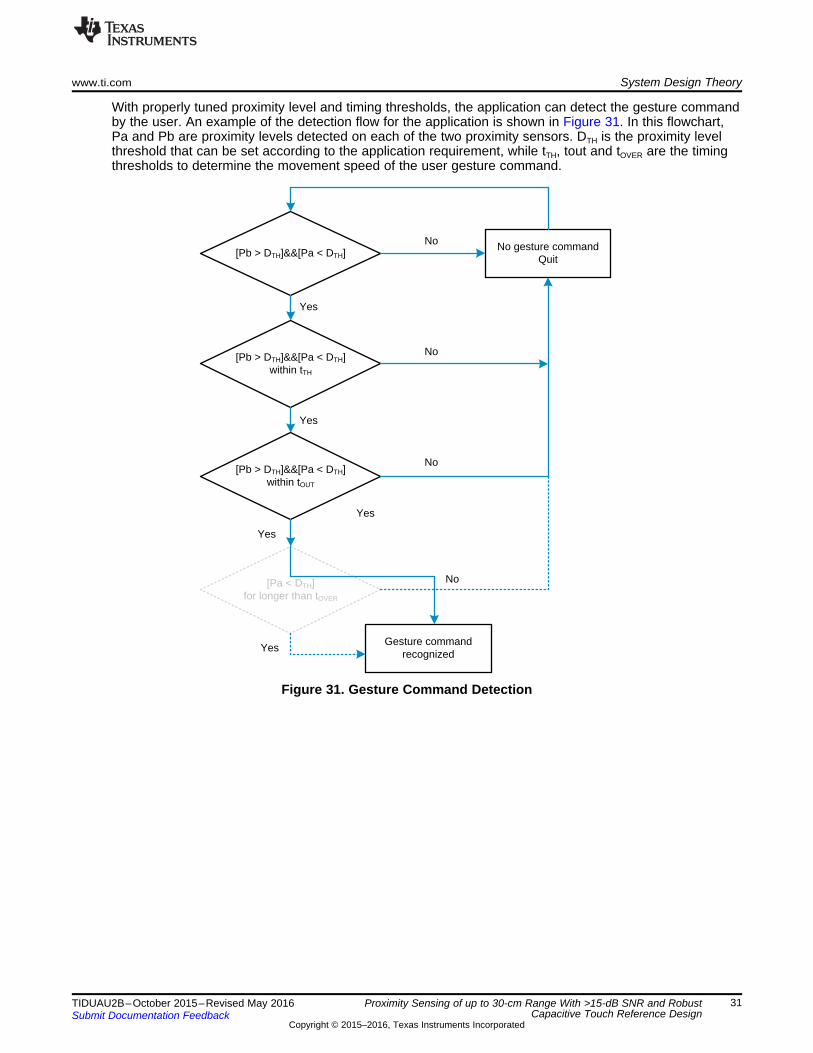
With properly tuned proximity level and timing thresholds, the application can detect the gesture commandby the user. An example of the detection flow for the application is shown in Figure 31. In this flowchart,Pa and Pb are proximity levels detected on each of the two proximity sensors. DTH is the proximity levelthreshold that can be set according to the application requirement, while tTH, tout and tOVER are the timingthresholds to determine the movement speed of the user gesture command.
Figure 31. Gesture Command Detection
Getting Started: Firmware www.ti.com
32 TIDUAU2B–October 2015–Revised May 2016Submit Documentation Feedback
Copyright © 2015–2016, Texas Instruments Incorporated
Proximity Sensing of up to 30-cm Range With >15-dB SNR and RobustCapacitive Touch Reference Design
6 Getting Started: FirmwareThis section describes how the firmware work and how to adjust the parameter settings to performcustomized tests.
6.1 Task HandlerA simple task handler is implemented in the firmware. When the program enters main routine, it performsan initialization of all the peripherals, driver modules, and tasks.
The task handler uses the internal watchdog timer of the MSP430 to generate a 0.5-ms interval and keepsticking in the ISR of the watchdog interval interrupt. A 32-bit counter Global_Timing_Counter holds thecounting of ticks in units of 1 ms.
In the main loop, taskHandler() is called to execute the active tasks at their pre-defined intervals. Thisfirmware has defined three tasks: taskA runs with period of 2 ms; taskB runs with period of 10 ms; taskCruns every 1 second. To change the task period, the user can use the configTask().
Starting and stopping the execution of one task can be done by calling startTask() and stopTask()routines. When calling startTask(), the user is able to assign a start offset time to the task to avoid multipletasks from being executed in the same time slot.
6.2 Configuring FDC2214 RegistersSource files drv_fdc2x14.c and drv_fdc2x14.h are provided for controlling the FDC2214 devices in thisdesign and can be re-used to customized applications based on MSP430 MCUs. In drv_fdc2x14.c, thefollowing function calls are implemented:• void fdc2x14Init(fdc2x14Control_t*)
This function initializes the set values of the FDC2214 registers into pre-defined global variables. Lateron, the set values are to be written into the FDC2214 registers. The parameter of the function is apointer to the data structure that holds the set values of the corresponding FDC2214 device.
• uint16_t fdc2x14GetRegister(fdc2x14Control_t*, enum_fdcRegAddr_t)This function returns the register value of the target register in the target FDC2214device given by theparameters. The internal registers of the FDC2214device are all with a 16-bit data length. Therefore,this function returns a 16-bit unsigned integer value, which can be later on cast into register bit maptypes.
• void fdc2x14SetRegister(fdc2x14Control_t*, enum_fdcRegAddr_t, uint16_t)This function sets the 16-bit unsigned integer value specified in the parameter into the target register ofthe target FDC2214 device.
• void fdc2x14Handler(fdc2x14Control_t*)The handler is to be executed in a task periodically. In the handler, the program determines theworking mode of the target FDC2214device and performs initialization, checking and reading theconversion results, and shutting down the device. In this design, this handler is called in the task with a10-ms period.
typedef union regSTATUS{
struct
{
unit16_t CH3_UNREADCONV : 1; //0
unit16_t CH2_UNREADCONV : 1; //1
unit16_t CH1_UNREADCONV : 1; //2
unit16_t CH0_UNREADCONV : 1; //3
unit16_t RESERVED0 : 2; //4-5
unit16_t DRDY : 1; //6
unit16_t RESERVED1 : 2; //7-8
unit16_t ERR_ALW : 1; //9
unit16_t ERR_AHW : 1; //10
unit16_t ERR_WD : 1; //11
unit16_t RESERVED2 : 2; //12-13
unit16_t ERR_CHAN : 2; //14-15
}bit;
uint16_t byte;
}regSTATUS_t;
www.ti.com Getting Started: Firmware
33TIDUAU2B–October 2015–Revised May 2016Submit Documentation Feedback
Copyright © 2015–2016, Texas Instruments Incorporated
Proximity Sensing of up to 30-cm Range With >15-dB SNR and RobustCapacitive Touch Reference Design
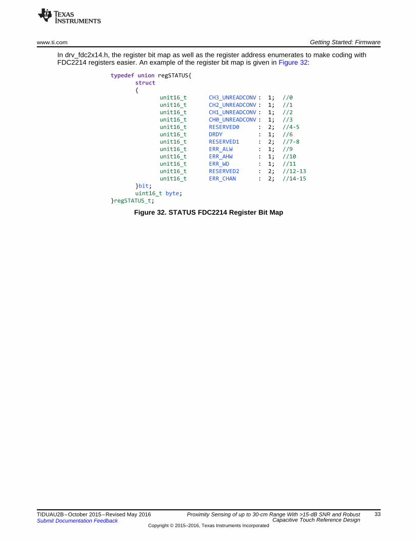
In drv_fdc2x14.h, the register bit map as well as the register address enumerates to make coding withFDC2214 registers easier. An example of the register bit map is given in Figure 32:
Figure 32. STATUS FDC2214 Register Bit Map
//HDC1050 Register bit definitions
typedef union regCONFIGURATION{
struct
{
unit16_t RESEVED0 : 8; //0-7
unit16_t HRES : 2; //8-9
unit16_t TRES : 1; //10
unit16_t BTST : 1; //11
unit16_t MODE : 1; //12
unit16_t HEAT : 1; //13
unit16_t RESERVED1 : 1; //14
unit16_t RST : 1; //15
}bit;
uint16_t byte;
}regCONFIGURATION_t;
Getting Started: Firmware www.ti.com
34 TIDUAU2B–October 2015–Revised May 2016Submit Documentation Feedback
Copyright © 2015–2016, Texas Instruments Incorporated
Proximity Sensing of up to 30-cm Range With >15-dB SNR and RobustCapacitive Touch Reference Design
6.3 Configuring HDC1050 RegistersSource files drv_hdc1050.c and drv_hdc1050.h control the HDC1050 device in this design and can be re-used to customized applications based on MSP430 MCUs. In drv_hdc1050.c, the following function callsare implemented:• void hdc1050Init(void):
This function initializes the set values of the HDC1050 registers into pre-defined global variables. Lateron, the set values are to be written into the HDC1050 registers.
• void hdc1050SetConfiguration(regCONFIGURATION_t) andvoid hdc1050GetConfiguration(regCONFIGURATION_t*):These two software driver level function calls set and get the configuration register of the HDC1050.
• void hdc1050TriggerConversion(enum_hdcRegAddr_t):Because the HDC1050 is, at default, working in sleep mode, the application needs to trigger theconversion of the HDC1050 with an I2C command. In this design, this function is defined as static.
• void hdc1050ReadConversionResults(void):This function reads out the conversion result on both humidity and temperature from the HDC1050 andconverts the results into units of %RH and °C. In this design, this function is defined as static.
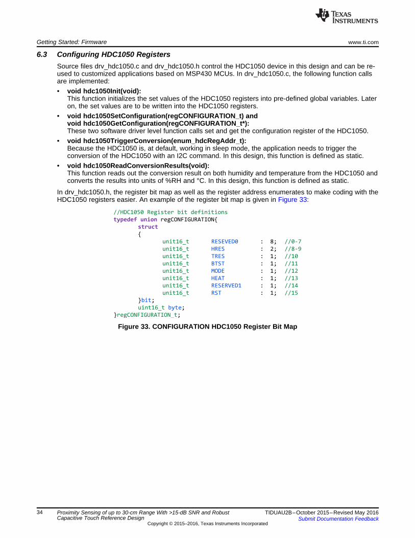
In drv_hdc1050.h, the register bit map as well as the register address enumerates to make coding with theHDC1050 registers easier. An example of the register bit map is given in Figure 33:
Figure 33. CONFIGURATION HDC1050 Register Bit Map
www.ti.com Test Results
35TIDUAU2B–October 2015–Revised May 2016Submit Documentation Feedback
Copyright © 2015–2016, Texas Instruments Incorporated
Proximity Sensing of up to 30-cm Range With >15-dB SNR and RobustCapacitive Touch Reference Design
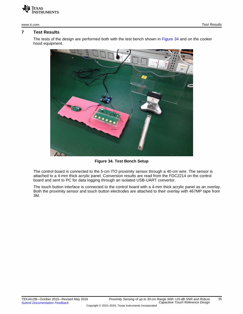
7 Test ResultsThe tests of the design are performed both with the test bench shown in Figure 34 and on the cookerhood equipment.
Figure 34. Test Bench Setup
The control board is connected to the 5-cm ITO proximity sensor through a 40-cm wire. The sensor isattached to a 4-mm thick acrylic panel. Conversion results are read from the FDC2214 on the controlboard and sent to PC for data logging through an isolated USB-UART convertor.
The touch button interface is connected to the control board with a 4-mm thick acrylic panel as an overlay.Both the proximity sensor and touch button electrodes are attached to their overlay with 467MP tape from3M.
Test Results www.ti.com
36 TIDUAU2B–October 2015–Revised May 2016Submit Documentation Feedback
Copyright © 2015–2016, Texas Instruments Incorporated
Proximity Sensing of up to 30-cm Range With >15-dB SNR and RobustCapacitive Touch Reference Design
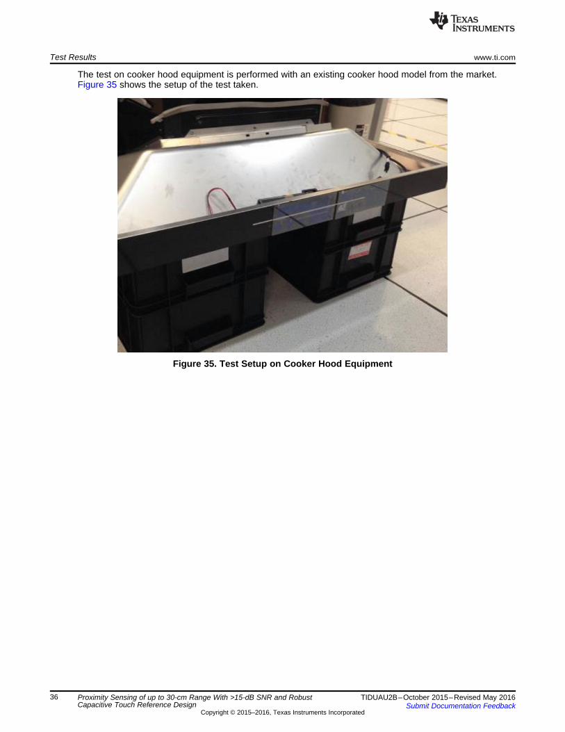
The test on cooker hood equipment is performed with an existing cooker hood model from the market.Figure 35 shows the setup of the test taken.
Figure 35. Test Setup on Cooker Hood Equipment
www.ti.com Test Results
37TIDUAU2B–October 2015–Revised May 2016Submit Documentation Feedback
Copyright © 2015–2016, Texas Instruments Incorporated
Proximity Sensing of up to 30-cm Range With >15-dB SNR and RobustCapacitive Touch Reference Design
7.1 ProximityThe hardware characteristic on proximity sensing circuit is tested both by reading the conversion resultsand by observation from the oscilloscope.
The test results are listed in Table 3:
Table 3. Static Parasitic Capacitance Built Up
TEST CONDITION AVERAGECOUNTS
EQUIVALENTCAPACITANCE (pF)
RESONANTFREQUENCY
(OSCILLOSCOPE)(MHz)
EQUIVALENTCAPACITANCE (pF) REMARK
Sensor, wire, and probe arenot present 36716045 14.01275973 — — —
Sensor and wire are notpresent, probe on 35383424 17.62066189 5.278 17.51600370 3.6 pF
Sensor is not present, 40-cm wire is connected, probeon
34616252 19.88925446 5.157 19.91435362 2.3 pF
5-cm ITO sensor and 40-cmwire on, probe on 33997918 21.83058614 5.066 21.83241667 1.9 pF
5-cm ITO sensor and 40-cmwire on, probe on with palmof hand in front at 10-cmdistance
33925504 22.06490777 5.058 22.00600553 0.2 pF
The test results listed here show the static parasite capacitance on the proximity sensing circuit of theboard of this design is roughly 14 pF. However, with a 40-cm long wire (not shielded), an additional 2.3 pFis added to the channel. The equivalent capacitance formed by the sensor electrode and the static labenvironment is roughly 1.9 pF.
The input capacitor of the passive probe of the oscilloscope is adding about 3.6 pF to the measurementand this has to be taken into consideration when probing the sensing circuit.
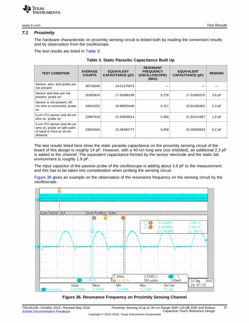
Figure 36 gives an example on the observation of the resonance frequency on the sensing circuit by theoscilloscope.
Figure 36. Resonance Frequency on Proximity Sensing Channel
( )POWER 10
Power of signalSNR dB 10 log
Power of noise
æ ö= ´ ç ÷
è ø
( )n 2
ii 0
Signal BaselinePower of signal
n
=-
=å
Time (ms)
Con
vers
ion
Res
ult (
Cou
nts)
0 5000 10000 15000 20000 25000 3000034468000
34470000
34472000
34474000
34476000
34478000
34480000
34482000
34484000
D003
CH1
Test Results www.ti.com
38 TIDUAU2B–October 2015–Revised May 2016Submit Documentation Feedback
Copyright © 2015–2016, Texas Instruments Incorporated
Proximity Sensing of up to 30-cm Range With >15-dB SNR and RobustCapacitive Touch Reference Design
The waveform is captured on CH1 of sensor 1 (U7) (TP21) against GND, with a 5-cm ITO sensor and40-cm wire on, probe on with palm of hand in front at 10-cm distance.
Proximity sensing test is performed by data logging from the FDC2214 conversion results. The settings onthe proximity sensing channels of FDC2214 device are:• Continuous sampling (AUTOSCAN = false)• Sensor full current activation (SENSOR_ACTIVATE_SEL = 0)• External 40-MHz crystal (REF_CLK_SRC = 1)• Deglitch at 10 MHz (DEGLITCH = 0x05)• fREFx = fCLK = 40 MHz (CHx_FIN_SEL = 1, CHx_FREF_DIVIDER = 1)• IDRIVE = 0.146 mA; Vpk = 1.76 V (CHx_IDRIVE = 0x0F)
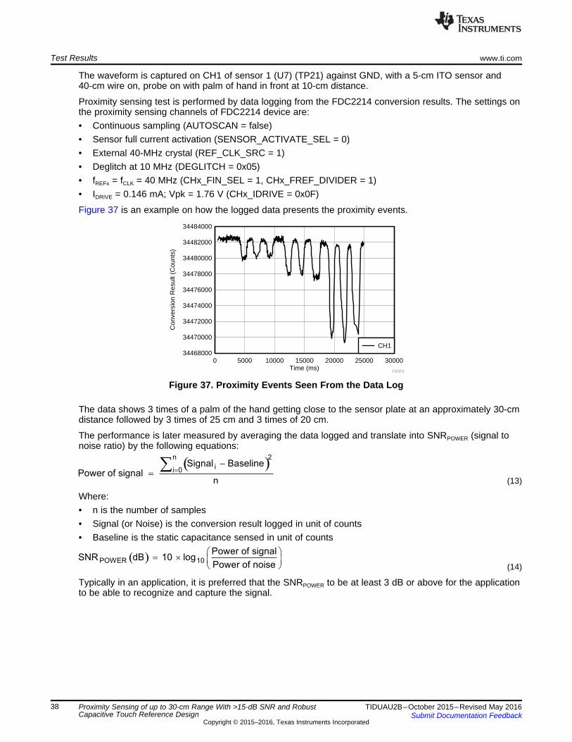
Figure 37 is an example on how the logged data presents the proximity events.
Figure 37. Proximity Events Seen From the Data Log
The data shows 3 times of a palm of the hand getting close to the sensor plate at an approximately 30-cmdistance followed by 3 times of 25 cm and 3 times of 20 cm.
The performance is later measured by averaging the data logged and translate into SNRPOWER (signal tonoise ratio) by the following equations:
(13)
Where:• n is the number of samples• Signal (or Noise) is the conversion result logged in unit of counts• Baseline is the static capacitance sensed in unit of counts
(14)
Typically in an application, it is preferred that the SNRPOWER to be at least 3 dB or above for the applicationto be able to recognize and capture the signal.
Distance of Object (cm)
SN
RP
OW
ER (
dB)
0 5 10 15 20 25 30 350
10
20
30
40
50
60
70
D001
5-cm ITO on Bench5-cm ITO on Hood10-cm ITO on Bench10-cm Copper on Bench
www.ti.com Test Results
39TIDUAU2B–October 2015–Revised May 2016Submit Documentation Feedback
Copyright © 2015–2016, Texas Instruments Incorporated
Proximity Sensing of up to 30-cm Range With >15-dB SNR and RobustCapacitive Touch Reference Design
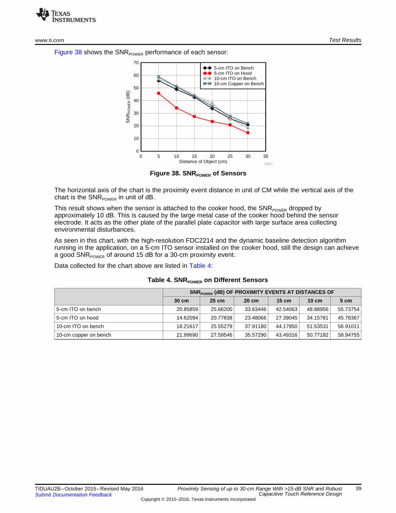
Figure 38 shows the SNRPOWER performance of each sensor:
Figure 38. SNRPOWER of Sensors
The horizontal axis of the chart is the proximity event distance in unit of CM while the vertical axis of thechart is the SNRPOWER in unit of dB.
This result shows when the sensor is attached to the cooker hood, the SNRPOWER dropped byapproximately 10 dB. This is caused by the large metal case of the cooker hood behind the sensorelectrode. It acts as the other plate of the parallel plate capacitor with large surface area collectingenvironmental disturbances.
As seen in this chart, with the high-resolution FDC2214 and the dynamic baseline detection algorithmrunning in the application, on a 5-cm ITO sensor installed on the cooker hood, still the design can achievea good SNRPOWER of around 15 dB for a 30-cm proximity event.
Data collected for the chart above are listed in Table 4:
Table 4. SNRPOWER on Different Sensors
SNRPOWER (dB) OF PROXIMITY EVENTS AT DISTANCES OF30 cm 25 cm 20 cm 15 cm 10 cm 5 cm
5-cm ITO on bench 20.85859 25.66200 33.63446 42.54063 48.88956 55.737545-cm ITO on hood 14.62094 20.77838 23.48066 27.39045 34.15781 45.7836710-cm ITO on bench 18.21617 25.55279 37.91180 44.17950 51.53531 56.9101110-cm copper on bench 21.99690 27.59546 35.57290 43.49316 50.77182 58.94755
Time (ms)
Con
vers
ion
Res
ult (
Cou
nts)
10000 12000 14000 16000 18000 2000034462000
34464000
34466000
34468000
34470000
34472000
34474000
34476000
34478000
34480000
D004
CH0CH1
Test Results www.ti.com
40 TIDUAU2B–October 2015–Revised May 2016Submit Documentation Feedback
Copyright © 2015–2016, Texas Instruments Incorporated
Proximity Sensing of up to 30-cm Range With >15-dB SNR and RobustCapacitive Touch Reference Design
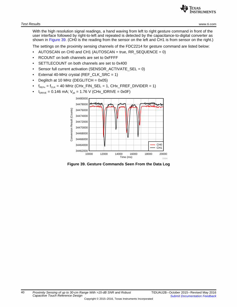
With the high resolution signal readings, a hand waving from left to right gesture command in front of theuser interface followed by right-to-left and repeated is detected by the capacitance-to-digital converter asshown in Figure 39. (CH0 is the reading from the sensor on the left and CH1 is from sensor on the right.)
The settings on the proximity sensing channels of the FDC2214 for gesture command are listed below:• AUTOSCAN on CH0 and CH1 (AUTOSCAN = true, RR_SEQUENCE = 0)• RCOUNT on both channels are set to 0xFFFF• SETTLECOUNT on both channels are set to 0x400• Sensor full current activation (SENSOR_ACTIVATE_SEL = 0)• External 40-MHz crystal (REF_CLK_SRC = 1)• Deglitch at 10 MHz (DEGLITCH = 0x05)• fREFx = fCLK = 40 MHz (CHx_FIN_SEL = 1, CHx_FREF_DIVIDER = 1)• IDRIVE = 0.146 mA; Vpk = 1.76 V (CHx_IDRIVE = 0x0F)
Figure 39. Gesture Commands Seen From the Data Log
Time (ms)
Con
vers
ion
Res
ult (
Cou
nts)
0 2000 4000 6000 8000 10000 12000 14000 1600012260000
12265000
12270000
12275000
12280000
12285000
12290000
12295000
D005
Key
www.ti.com Test Results
41TIDUAU2B–October 2015–Revised May 2016Submit Documentation Feedback
Copyright © 2015–2016, Texas Instruments Incorporated
Proximity Sensing of up to 30-cm Range With >15-dB SNR and RobustCapacitive Touch Reference Design
7.2 Touch ButtonsThe touch button test is performed on Key3 and Key4 of the 6-button touch circuit board. The settings onthe touch button channels of FDC2214 device are listed as follows:• Scan sampling on CH0, CH1, CH2, CH3 (AUTOSCAN = true)• Scan sequence: CH0, CH1, CH2, CH3 (RR_SEQUENCE = 0x02)• Sensor full current activation (SENSOR_ACTIVATE_SEL = 0)• External 40-MHz crystal (REF_CLK_SRC = 1)• Deglitch at 10 MHz (DEGLITCH = 0x05)• Same settings on all channels• Reference count = 0xffff• Settle count = 0x400• fREFx = fCLK = 40 MHz (CHx_FIN_SEL = 1, CHx_FREF_DIVIDER = 1)• IDRIVE = 1.006 mA; Vpk = 1.70 V (CHx_IDRIVE = 0x1C)
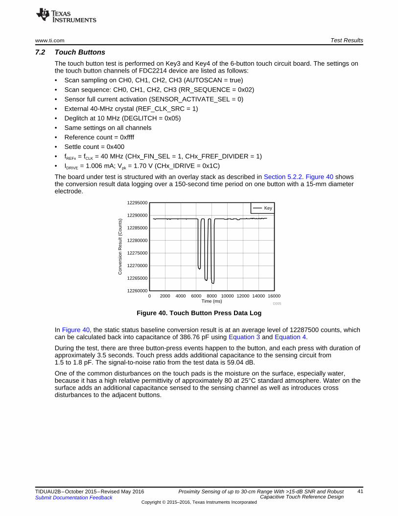
The board under test is structured with an overlay stack as described in Section 5.2.2. Figure 40 showsthe conversion result data logging over a 150-second time period on one button with a 15-mm diameterelectrode.
Figure 40. Touch Button Press Data Log
In Figure 40, the static status baseline conversion result is at an average level of 12287500 counts, whichcan be calculated back into capacitance of 386.76 pF using Equation 3 and Equation 4.
During the test, there are three button-press events happen to the button, and each press with duration ofapproximately 3.5 seconds. Touch press adds additional capacitance to the sensing circuit from1.5 to 1.8 pF. The signal-to-noise ratio from the test data is 59.04 dB.
One of the common disturbances on the touch pads is the moisture on the surface, especially water,because it has a high relative permittivity of approximately 80 at 25°C standard atmosphere. Water on thesurface adds an additional capacitance sensed to the sensing channel as well as introduces crossdisturbances to the adjacent buttons.
Time (ms)
Con
vers
ion
Res
ult (
Cou
nts)
0 4000 8000 12000 16000 2000012240000
12250000
12260000
12270000
12280000
12290000
12300000
12310000
12320000
D006
Key3Key4
Test Results www.ti.com
42 TIDUAU2B–October 2015–Revised May 2016Submit Documentation Feedback
Copyright © 2015–2016, Texas Instruments Incorporated
Proximity Sensing of up to 30-cm Range With >15-dB SNR and RobustCapacitive Touch Reference Design
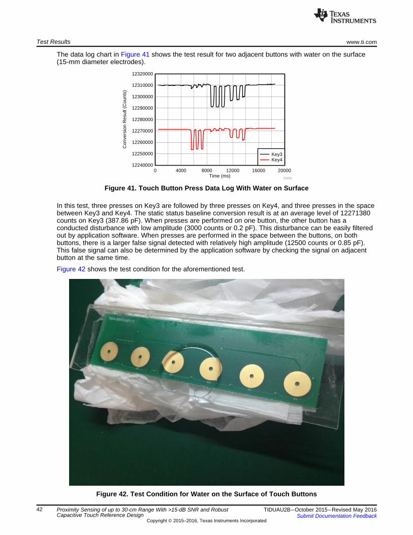
The data log chart in Figure 41 shows the test result for two adjacent buttons with water on the surface(15-mm diameter electrodes).
Figure 41. Touch Button Press Data Log With Water on Surface
In this test, three presses on Key3 are followed by three presses on Key4, and three presses in the spacebetween Key3 and Key4. The static status baseline conversion result is at an average level of 12271380counts on Key3 (387.86 pF). When presses are performed on one button, the other button has aconducted disturbance with low amplitude (3000 counts or 0.2 pF). This disturbance can be easily filteredout by application software. When presses are performed in the space between the buttons, on bothbuttons, there is a larger false signal detected with relatively high amplitude (12500 counts or 0.85 pF).This false signal can also be determined by the application software by checking the signal on adjacentbutton at the same time.
Figure 42 shows the test condition for the aforementioned test.
Figure 42. Test Condition for Water on the Surface of Touch Buttons
www.ti.com Test Results
43TIDUAU2B–October 2015–Revised May 2016Submit Documentation Feedback
Copyright © 2015–2016, Texas Instruments Incorporated
Proximity Sensing of up to 30-cm Range With >15-dB SNR and RobustCapacitive Touch Reference Design
7.3 LEDThe following waveforms show the LED current and dimming control signal from the MSP430 at 250 Hz.
Channel 4 of the oscilloscope waveforms is the LED current and Channel 1 is the dimming control PWMfrom MSP430.
Figure 43. LED Current and Dimming Signal at 50% Duty Cycle
Figure 44. LED Current and Dimming Signal at 10% Duty Cycle
Test Results www.ti.com
44 TIDUAU2B–October 2015–Revised May 2016Submit Documentation Feedback
Copyright © 2015–2016, Texas Instruments Incorporated
Proximity Sensing of up to 30-cm Range With >15-dB SNR and RobustCapacitive Touch Reference Design
Figure 45. LED Current and Dimming Signal at 99% Duty Cycle
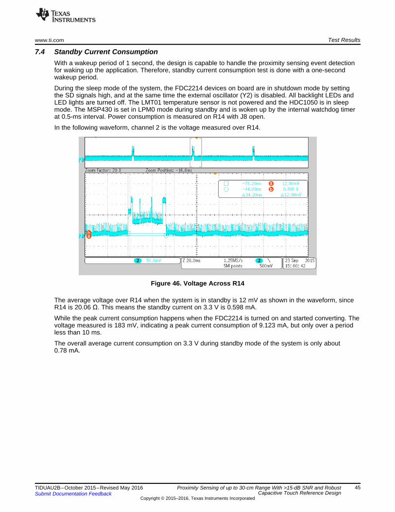
www.ti.com Test Results
45TIDUAU2B–October 2015–Revised May 2016Submit Documentation Feedback
Copyright © 2015–2016, Texas Instruments Incorporated
Proximity Sensing of up to 30-cm Range With >15-dB SNR and RobustCapacitive Touch Reference Design
7.4 Standby Current ConsumptionWith a wakeup period of 1 second, the design is capable to handle the proximity sensing event detectionfor waking up the application. Therefore, standby current consumption test is done with a one-secondwakeup period.
During the sleep mode of the system, the FDC2214 devices on board are in shutdown mode by settingthe SD signals high, and at the same time the external oscillator (Y2) is disabled. All backlight LEDs andLED lights are turned off. The LMT01 temperature sensor is not powered and the HDC1050 is in sleepmode. The MSP430 is set in LPM0 mode during standby and is woken up by the internal watchdog timerat 0.5-ms interval. Power consumption is measured on R14 with J8 open.
In the following waveform, channel 2 is the voltage measured over R14.
Figure 46. Voltage Across R14
The average voltage over R14 when the system is in standby is 12 mV as shown in the waveform, sinceR14 is 20.06 Ω. This means the standby current on 3.3 V is 0.598 mA.
While the peak current consumption happens when the FDC2214 is turned on and started converting. Thevoltage measured is 183 mV, indicating a peak current consumption of 9.123 mA, but only over a periodless than 10 ms.
The overall average current consumption on 3.3 V during standby mode of the system is only about0.78 mA.
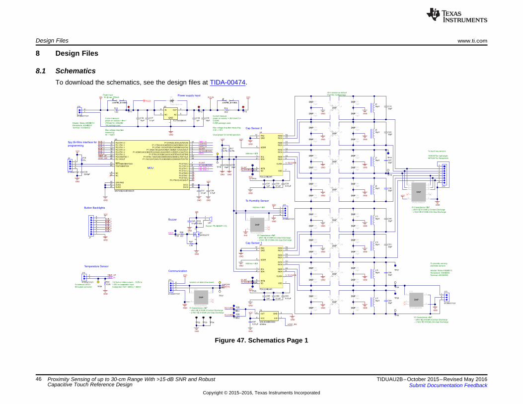
SCL1
SDA2
CLKIN3
ADDR4
INTB5
SD6
VDD7
GND8
IN0A9
IN0B10
IN1A11
IN1B12
PAD17
IN2A13
IN2B14
IN3A15
IN3B16
U4
FDC2214RGHR
18µH
L3
1 234
L4DNP
18pF
C11DNP
33pF
C13
VCC4
E/D1
GND2
OUT3
40 MHz
Y2
625L3C040M00000
1
GND
OUT3
IN2
NC4
NC5
U3
TLV70433DBVR
VIN
Power Input:
9V @ max. 750mA
1.00
R13
12J7
JUMPER_2X100MIL
Current measure:
power on resistor = 1ohm *
(750mA)^2 = 0.5625W.
1W package used.
Max voltage drop when
measuring:
9V -> 8.25V
VLED
3V3_IN
GND
1µF
C18
10µF
C19
10µF
C16
12J8
JUMPER_2X100MIL
VCC
Current measure:
power on resistor = 20* (10mA)^2 =
0.002W.
0.25W package used.
Max voltage drop when measuring:
3.3V -> 3.1V
Close jumper for normal operation.
18pF
C14DNP GND
18pF
C12DNP
18pF
C15DNP GND
18µH
L5
1 234
L6DNP
18pF
C20DNP
33pF
C22
18pF
C23DNP GND
18pF
C21DNP
18pF
C24DNP GND
18µH
L7
1 234
L8DNP
18pF
C25DNP
33pF
C27
18pF
C28DNP GND
18pF
C26DNP
18pF
C29DNP GND
18µH
L9
1 234
L10DNP
18pF
C34DNP
33pF
C36
18pF
C39DNP GND
18pF
C35DNP
18pF
C40DNP GND
SCL1
SDA2
CLKIN3
ADDR4
INTB5
SD6
VDD7
GND8
IN0A9
IN0B10
IN1A11
IN1B12
PAD17
IN2A13
IN2B14
IN3A15
IN3B16
U7
FDC2214RGHR
18µH
L11
1 234
L12DNP
18pF
C42DNP
33pF
C44
18pF
C46DNP GND
18pF
C43DNP
18pF
C47DNP GND
18µH
L13
1 234
L14DNP
18pF
C49DNP
33pF
C51
18pF
C52DNP GND
18pF
C50DNP
18pF
C53DNP GND
18µH
L15
1 234
L16DNP
18pF
C54DNP
33pF
C56
18pF
C57DNP GND
18pF
C55DNP
18pF
C58DNP GND
18µH
L17
1 234
L18DNP
18pF
C62DNP
33pF
C64
18pF
C65DNP GND
18pF
C63DNP
18pF
C66DNP GND
Header: Molex 43650-0313
Receptacle: 43645-0300
Terminal: 43030-0002
GND
VCC
GND
1µF
C59
GND
VCC
To proximity sensing
electrode sensors
GND
GND
Address = 0x2A
1µF
C31
GND
VCC
GND
Address = 0x2B
VCC
P1.1/TA0.0/UCA0RXD/UCA0SOMI/A1/CA11
P1.2/TA0.1/UCA0TXD/UCA0SIMO/A2/CA22
P1.3/ADC10CLK/A3/VREF-/VEREF-/CA3/CAOUT3
P1.4/SMCLK/UCB0STE/UCA0CLK/A4/VREF+/VEREF+/CA4/TCK4
P1.5/TA0.0/UCB0CLK/UCA0STE/A5/CA5/TMS5
P3.1/TA1.06
P3.0/TA0.27
P3.2/TA1.112
P3.3/TA1.213
P3.4/TA0.014
P3.5/TA0.118
P3.6/TA0.219
P3.7/TA1CLK/CAOUT20
P1.6/TA0.1/A6/CA6/UCB0SOMI/UCB0SCL/TDI/TCLK21
P1.7/A7/CA7/CAOUT/UCB0SIMO/UCB0SDA/TDO/TDI22
RST/NMI/SBWTDIO23
TEST/SBWTCK24
AVCC29
DVCC30
P1.0/TA0CLK/ACLK/A0/CA031
NC8
P2.0/TA1.09
P2.1/TA1.110
P2.2/TA1.111
P2.3/TA1.015
P2.4/TA1.216
P2.5/TA1.217
P2.7/XOUT25
P2.6/XIN/TA0.126
DVSS27
DVSS28
NC32
QFN PAD33
U5
MSP430G2553IRHB32R
1
2
LS1
Buzzer: PB-12N32MP-12Q
4.75k
R16
VCC
4.75k
R17
Address = 0x40
GND
VCC
GND GND
4
1
2
3
J9
61300411121
GND
47k
R18
VCC
2200pF
C30
Spy Bi-Wire interface for
programming
D5
1N5819HW-7-F
DNP
Power supply input
1
2
J14
61300211121
TEMP_VP
To external LMT01
Shrouded connector
112.5uA to 143uA current - 1.125V to
1.43V on comparator input.
Comparator Vref = 0.25Vcc = 0.825V
2.00k
R19
1
23
Q1
2N7002-7-F
3.3k
R27
100
R26
GND
GND
VIN
BEEP
Button Backlights
Temperature Sensor
Buzzer
MCU
S1_INT
S1_SHUTDOWN
S2_INT
S2_SHUTDOWN
Cap Sensor 2
Cap Sensor 1
To Humidity Sensor
5
4
1
2
3
6
7
8
J10
To touch key sensors
487526-7 for Receptacle
103634-7 for right angle
S2_SHUTDOWN
S2_INT
TEMP_IN
4
1
2
3
J11
61300411121
UART_TX
UART_RX
VCC
GND
UART_RX
UART_TX
Communication
Isolation on motor drive board
S1_INT
S1_SHUTDOWN
BEEP
BLED_1
BLED_2
BLED_3
BLED_4
BLED_5
BLED_6
TEMP_VP
LED_DIM_1
LED_DIM_2
Header: Molex 43650-0213
Receptacle: 43645-0200
Terminal: 43030-0002
1
2
J16
61300211121
S1_CLKIN
S2_CLKIN
S1_CLKIN
S2_CLKIN
33.0
R38
33.0
R39
4
1
2
3
J17
61300411121
VCC
GND
33pF
C41
33pF
C68
GND GND
GND
0hm resistor as default
Pad fitts 1206package
TP14
TP18
TP30
TP28
TP26TP23
TP27
TP15
TP16
TP11 TP12 TP13
TP17
TP19
TP22
TP25
TP29
TP31
TP32 TP33 TP34
GND
TP20
TP24
TP21
NC1
NC2
IO13
GND4
IO25
U10
TPD2E2U06DRL
DNP
NC1
NC2
IO13
GND4
IO25
U11
TPD2E2U06DRL
DNP
NC1
NC2
IO13
GND4
IO25
U12
TPD2E2U06DRL
DNP
GND
IO11
IO22
IO33
NC4
GND5
IO46
IO57
IO68
NC9
VCC10
U9
TPD6E001RSER
DNP
VCC
IO Capacitance = 1.5pF
– ±8-kV IEC 61000-4-2Contact Discharge
– ±15-kV IEC 61000-4-2Air-Gap Discharge
IO Capacitance = 1.5pF
– ±8-kV IEC 61000-4-2Contact Discharge
– ±15-kV IEC 61000-4-2Air-Gap Discharge
IO Capacitance = 1.5pF
– ±8-kV IEC 61000-4-2Contact Discharge
– ±15-kV IEC 61000-4-2Air-Gap Discharge
IO Capacitance = 1.5pF
– ±8-kV IEC 61000-4-2Contact Discharge
– ±15-kV IEC 61000-4-2Air-Gap Discharge
GND
4.7µF
C38
10.0k
R33
GND
TEMP_IN
5
4
1
2
3
6
7
8
J?
VCC
GND
BLED_1
BLED_2
BLED_3
BLED_4
BLED_5
BLED_6
1
2
3
J13
61300311121
0.1µF
C32
0.1µF
C17
0.1µF
C37
0.1µF
C45
0.1µF
C60
0.01µF
C33
0.01µF
C61
0.01µF
C67
20.0
R14
nOSC_EN
nOSC_EN
Design Files www.ti.com
46 TIDUAU2B–October 2015–Revised May 2016Submit Documentation Feedback
Copyright © 2015–2016, Texas Instruments Incorporated
Proximity Sensing of up to 30-cm Range With >15-dB SNR and RobustCapacitive Touch Reference Design
8 Design Files
8.1 SchematicsTo download the schematics, see the design files at TIDA-00474.
Figure 47. Schematics Page 1
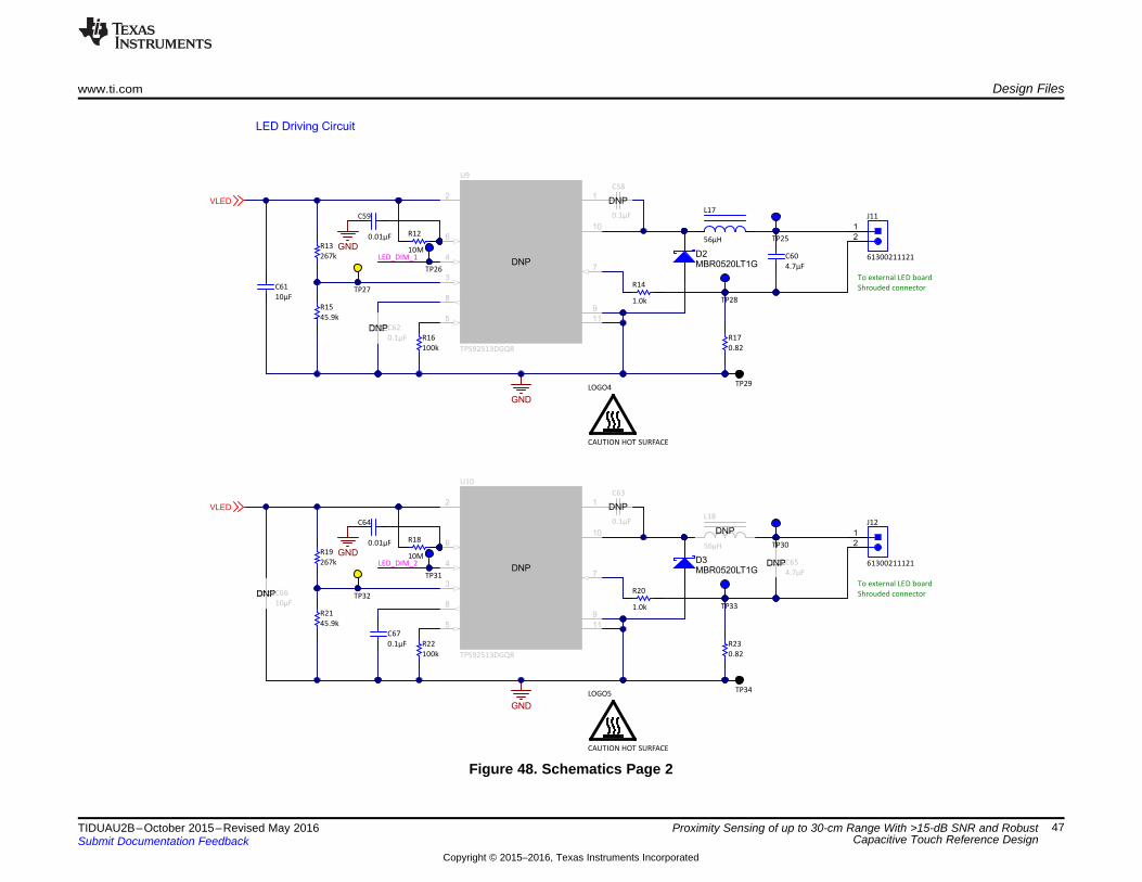
1
2
J11
61300211121
To external LED board
Shrouded connector
BOOT1
VIN2
UVLO3
PDIM4
RT/CLK5
IADJ6
ISENSE7
COMP8
GND9
PH10
PAD11
U9
TPS92513DGQR
DNP
LOGO4
CAUTION HOT SURFACE
100k
R16
GND
GND
0.1µF
C58
DNP
56µH
L17
4.7µF
C60
10µF
C61
0.1µF
C62DNP
10M
R12
1.0k
R14
0.01µF
C59
267k
R13
45.9k
R15
VLED
0.82
R17
1
2
J12
61300211121
To external LED board
Shrouded connector
BOOT1
VIN2
UVLO3
PDIM4
RT/CLK5
IADJ6
ISENSE7
COMP8
GND9
PH10
PAD11
U10
TPS92513DGQR
DNP
LOGO5
CAUTION HOT SURFACE
100k
R22
GND
GND
0.1µF
C63
DNP
56µH
L18
DNP
4.7µF
C65DNP
10µF
C66DNP
0.1µF
C67
10M
R18
1.0k
R20
0.01µF
C64
267k
R19
45.9k
R21
VLED
0.82
R23
LED_DIM_1
LED_DIM_2
LED Driving Circuit
TP26
TP31
TP32
TP27
TP33
TP28
TP34
TP29
TP25
TP30
D2MBR0520LT1G
D3MBR0520LT1G
www.ti.com Design Files
47TIDUAU2B–October 2015–Revised May 2016Submit Documentation Feedback
Copyright © 2015–2016, Texas Instruments Incorporated
Proximity Sensing of up to 30-cm Range With >15-dB SNR and RobustCapacitive Touch Reference Design
Figure 48. Schematics Page 2
Design Files www.ti.com
48 TIDUAU2B–October 2015–Revised May 2016Submit Documentation Feedback
Copyright © 2015–2016, Texas Instruments Incorporated
Proximity Sensing of up to 30-cm Range With >15-dB SNR and RobustCapacitive Touch Reference Design
8.2 Bill of MaterialsTo download the bill of materials (BOM), see the design files at TIDA-00474.
8.3 PCB LayoutTo download the PCB layout, see the design files at TIDA-00474.
8.4 Altium ProjectTo download the Altium project files, see the design files at TIDA-00474.
8.5 Gerber FilesTo download the Gerber files, see the design files at TIDA-00474.
9 References
1. Texas Instruments, Capacitive Touch Hardware Design Guide, MSP430 Design Guide (SLAA576)2. Texas Instruments, Backlight and Smart Lighting Control by Ambient Light and Proximity Sensor,
TIDA-00373 Design Guide (TIDU781)3. Texas Instruments, FDC1004: Basics of Capacitive Sensing and Applications, FDC1004 Application
Report (SNOA927)4. Texas Instruments, Capacitive Proximity Sensing Using the FDC1004, FDC1004 Application Report
(SNOA928)5. National Institute of Standards and Technology, Static Dielectric Constant of Water and Steam
(www.nist.gov/data/PDFfiles/jpcrd172.pdf)
10 About the AuthorLEBO "RENTON" MA joined TI as a system engineer in Shanghai and supported Hercules and theC2000™ family since 2012. Renton came to TI from Renesas Electronics where he was a field applicationengineer and later a technical marketing for body applications in automotive market for MCUs for sevenyears. After joining TI, Renton designed firmware and core logic on modeling tools for automotiveapplications and residential air conditioning systems. Renton has bachelor degrees in electronicengineering and English from Dalian University of Technology.
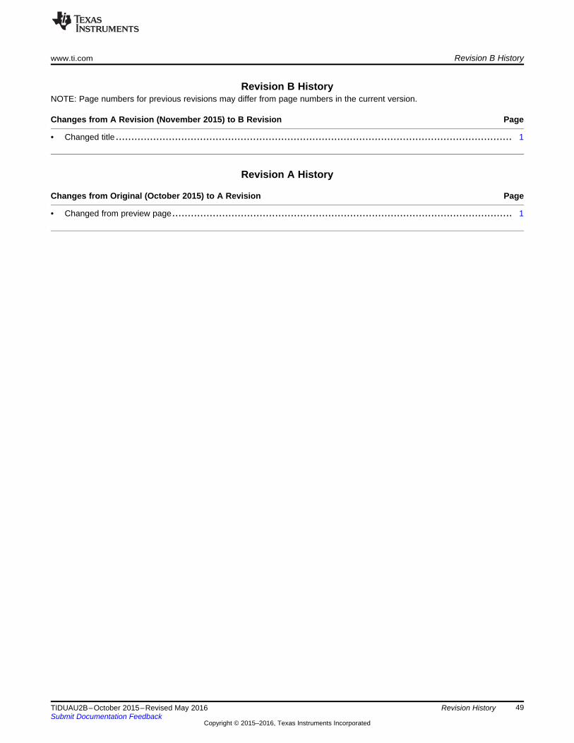
www.ti.com Revision B History
49TIDUAU2B–October 2015–Revised May 2016Submit Documentation Feedback
Copyright © 2015–2016, Texas Instruments Incorporated
Revision History
Revision B HistoryNOTE: Page numbers for previous revisions may differ from page numbers in the current version.
Changes from A Revision (November 2015) to B Revision ........................................................................................... Page
• Changed title............................................................................................................................... 1
Revision A History
Changes from Original (October 2015) to A Revision .................................................................................................... Page
• Changed from preview page............................................................................................................. 1

IMPORTANT NOTICE FOR TI REFERENCE DESIGNS
Texas Instruments Incorporated (‘TI”) reference designs are solely intended to assist designers (“Designer(s)”) who are developing systemsthat incorporate TI products. TI has not conducted any testing other than that specifically described in the published documentation for aparticular reference design.TI’s provision of reference designs and any other technical, applications or design advice, quality characterization, reliability data or otherinformation or services does not expand or otherwise alter TI’s applicable published warranties or warranty disclaimers for TI products, andno additional obligations or liabilities arise from TI providing such reference designs or other items.TI reserves the right to make corrections, enhancements, improvements and other changes to its reference designs and other items.Designer understands and agrees that Designer remains responsible for using its independent analysis, evaluation and judgment indesigning Designer’s systems and products, and has full and exclusive responsibility to assure the safety of its products and compliance ofits products (and of all TI products used in or for such Designer’s products) with all applicable regulations, laws and other applicablerequirements. Designer represents that, with respect to its applications, it has all the necessary expertise to create and implementsafeguards that (1) anticipate dangerous consequences of failures, (2) monitor failures and their consequences, and (3) lessen thelikelihood of failures that might cause harm and take appropriate actions. Designer agrees that prior to using or distributing any systemsthat include TI products, Designer will thoroughly test such systems and the functionality of such TI products as used in such systems.Designer may not use any TI products in life-critical medical equipment unless authorized officers of the parties have executed a specialcontract specifically governing such use. Life-critical medical equipment is medical equipment where failure of such equipment would causeserious bodily injury or death (e.g., life support, pacemakers, defibrillators, heart pumps, neurostimulators, and implantables). Suchequipment includes, without limitation, all medical devices identified by the U.S. Food and Drug Administration as Class III devices andequivalent classifications outside the U.S.Designers are authorized to use, copy and modify any individual TI reference design only in connection with the development of endproducts that include the TI product(s) identified in that reference design. HOWEVER, NO OTHER LICENSE, EXPRESS OR IMPLIED, BYESTOPPEL OR OTHERWISE TO ANY OTHER TI INTELLECTUAL PROPERTY RIGHT, AND NO LICENSE TO ANY TECHNOLOGY ORINTELLECTUAL PROPERTY RIGHT OF TI OR ANY THIRD PARTY IS GRANTED HEREIN, including but not limited to any patent right,copyright, mask work right, or other intellectual property right relating to any combination, machine, or process in which TI products orservices are used. Information published by TI regarding third-party products or services does not constitute a license to use such productsor services, or a warranty or endorsement thereof. Use of the reference design or other items described above may require a license from athird party under the patents or other intellectual property of the third party, or a license from TI under the patents or other intellectualproperty of TI.TI REFERENCE DESIGNS AND OTHER ITEMS DESCRIBED ABOVE ARE PROVIDED “AS IS” AND WITH ALL FAULTS. TI DISCLAIMSALL OTHER WARRANTIES OR REPRESENTATIONS, EXPRESS OR IMPLIED, REGARDING THE REFERENCE DESIGNS OR USE OFTHE REFERENCE DESIGNS, INCLUDING BUT NOT LIMITED TO ACCURACY OR COMPLETENESS, TITLE, ANY EPIDEMIC FAILUREWARRANTY AND ANY IMPLIED WARRANTIES OF MERCHANTABILITY, FITNESS FOR A PARTICULAR PURPOSE, AND NON-INFRINGEMENT OF ANY THIRD PARTY INTELLECTUAL PROPERTY RIGHTS.TI SHALL NOT BE LIABLE FOR AND SHALL NOT DEFEND OR INDEMNIFY DESIGNERS AGAINST ANY CLAIM, INCLUDING BUT NOTLIMITED TO ANY INFRINGEMENT CLAIM THAT RELATES TO OR IS BASED ON ANY COMBINATION OF PRODUCTS ASDESCRIBED IN A TI REFERENCE DESIGN OR OTHERWISE. IN NO EVENT SHALL TI BE LIABLE FOR ANY ACTUAL, DIRECT,SPECIAL, COLLATERAL, INDIRECT, PUNITIVE, INCIDENTAL, CONSEQUENTIAL OR EXEMPLARY DAMAGES IN CONNECTION WITHOR ARISING OUT OF THE REFERENCE DESIGNS OR USE OF THE REFERENCE DESIGNS, AND REGARDLESS OF WHETHER TIHAS BEEN ADVISED OF THE POSSIBILITY OF SUCH DAMAGES.TI’s standard terms of sale for semiconductor products (http://www.ti.com/sc/docs/stdterms.htm) apply to the sale of packaged integratedcircuit products. Additional terms may apply to the use or sale of other types of TI products and services.Designer will fully indemnify TI and its representatives against any damages, costs, losses, and/or liabilities arising out of Designer’s non-compliance with the terms and provisions of this Notice.IMPORTANT NOTICE
Mailing Address: Texas Instruments, Post Office Box 655303, Dallas, Texas 75265Copyright © 2016, Texas Instruments Incorporated