psoc short course day 1 introduction to psoc - mitweb.mit.edu/6.115/www/document/psoc_intro.pdf ·...
TRANSCRIPT

CYPRESS CONFIDENTIAL
Q1 2013
PSoC Short CourseDay 1
INTRODUCTION TO PSoC®

INTRODUCTION TO PSOC 3 AND PSOC 5 2CYPRESS
Before we begin
Install PSoC Creator (if you haven’t already)§ Copy PSoCCreatorSetup_2.1.exe from thumbdrive onto
local machine§ Launch PSoCCreatorSetup_2.1.exe§ Follow installation prompts (typical)§ Raise hands for issues / questions
Load Presentation and Labs§ Copy Intro_To_PSoC5.Bundle01.cywrk.Archive01.zip to
local machine§ Unzip file to preferred folders§ Double Click “Intro_To_PSoC5.Bundle01.cywrk”

INTRODUCTION TO PSOC 3 AND PSOC 5 3CYPRESS
Agenda
Time Topic10:00 – 10:15 am Course Introduction and Overview10:15 – 11:45 am PSoC Architecture Overview11:45 – 1:00 pm Lunch
1:00 – 2:00 pm SW Demo and Architecture Overview Lab
2:00 – 2:30 pm System Resources 2:30 – 3:00 pm System Resources Lab3:00 – 3:30 pm Break3:30 – 4:00 pm Digital Peripherals
4:00 – 4:30 pm Digital Peripherals Lab
4:30 – 5:00 pm Analog Peripherals
10:00 – 10:45 am (Wed.) Analog Peripherals Lab

INTRODUCTION TO PSOC 3 AND PSOC 5 4CYPRESS
Section Objectives
At the end of this section you will be able to
§ Understand the major differences between PSoC 1/3/5§ Understand the high-level architecture of PSoC 3/5§ Understand the CPU, Digital, Analog and Programmable
Routing / Interconnect Systems of PSoC 5

INTRODUCTION TO PSOC 3 AND PSOC 5 5CYPRESS
PSoC is a true programmable embedded SoC integrating configurable analog and digital peripheral functions,
memory and a microcontroller on a single chip.
WHAT IS PSoC®?
10 years+ of explosive PSoC growth
Thousands of active PSoC customers
Over One billion PSoC units shipped
PSoC is Everywhere!
(including over 700 universities)

INTRODUCTION TO PSOC 3 AND PSOC 5 6CYPRESS
INDUSTRIAL ENTERTAINMENT/DISPLAYS
SECURITY/MONITORINGHANDHELD DEVICES APPLIANCES
TOYS/GAMING DIGITAL PHOTOGRAPHY
SPORTS/ FITNESS COMPUTERS PRESENTER
TOOLS HOME THEATER
PSoC Is Everywhere!
INTRODUCTION TO PSOC 3 AND PSOC 5 7CYPRESS
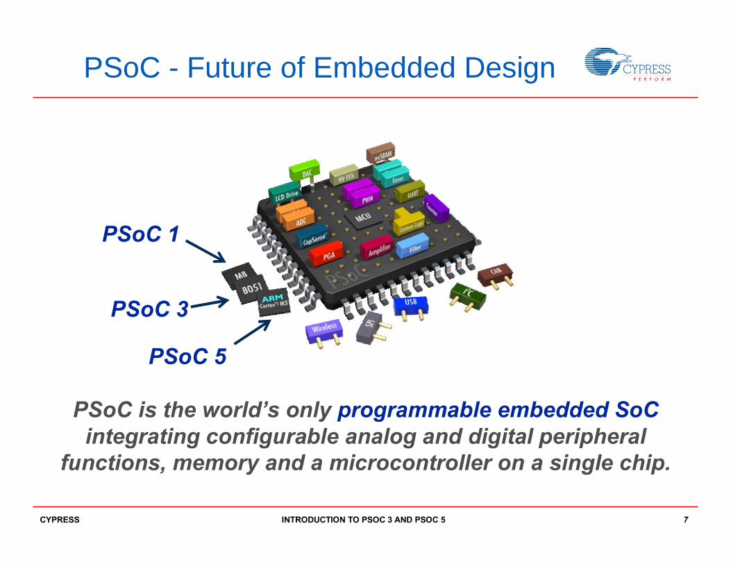
PSoC - Future of Embedded Design
PSoC is the world’s only programmable embedded SoCintegrating configurable analog and digital peripheral
functions, memory and a microcontroller on a single chip.
PSoC 3
PSoC 5
PSoC 1

INTRODUCTION TO PSOC 3 AND PSOC 5 8CYPRESS
PSoC 1 Device Overview
M8C MicrocontrollerUp to 24 MHz, 4 MIPS
Flash Memory 4 KB to 32 KB for program storage
SRAM 256B to 2 KB for data storage
Configurable Analog FunctionsImplement ADCs, DACs, filters, amplifiers, comparators, etc.
Configurable Digital FunctionsImplement timers, counters, PWMs, UART, SPI, IrDA, etc.
USES PSOC DESIGNER SOFTWARE

INTRODUCTION TO PSOC 3 AND PSOC 5 9CYPRESS
PSoC 1 Architecture
USES PSOC DESIGNER SOFTWARE

10
ARCHITECTURE OVERVIEWINTRODUCTION TO PSOC 3/5

INTRODUCTION TO PSOC 3 AND PSOC 5 11CYPRESS
PSoC 3 / PSoC 5 Platform Architecture
USES PSOC CREATOR SOFTWARE

INTRODUCTION TO PSOC 3 AND PSOC 5 12CYPRESS
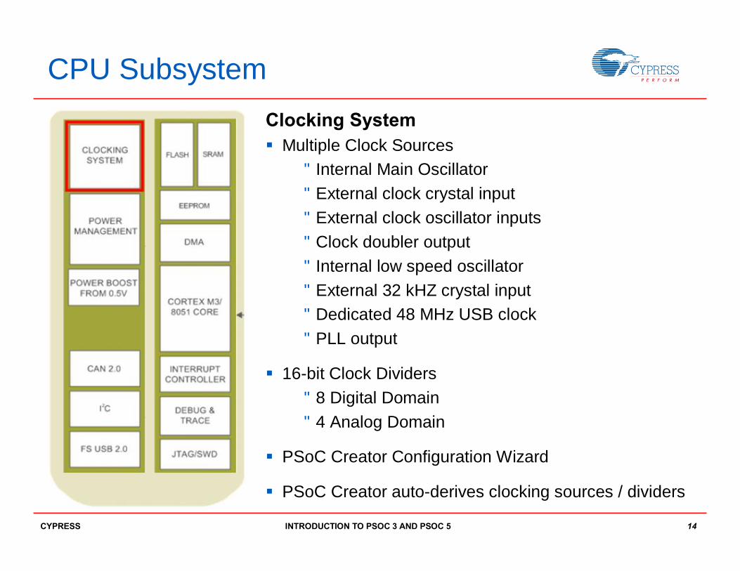
CPU Subsystem
ARM Cortex-M3§ Industry’s leading embedded CPU company§ Broad support for middleware and applications§ Upto 67 MHz; 83 DMIPS§ Enhanced v7 ARM architecture§ Thumb2 Instruction Set§ 16- and 32-bit Instructions (no mode switching)§ 32-bit ALU; Hardware multiply and divide§ Single cycle 3-stage pipeline; Harvard architecture
8051§ Broad base of existing code and support§ Upto 67 Mhz; 33 MIPS§ Single cycle instruction set

INTRODUCTION TO PSOC 3 AND PSOC 5 13CYPRESS
High Performance Memory§ Flash Memory with ECC§ High ratio of SRAM to flash§ EEPROM
Powerful DMA Engine§ 24-Channel Direct Memory Access§ Access to all Digital and Analog Peripherals§ CPU and DMA simultaneous access to
independent SRAM blocks
On-Chip Debug and Trace§ Industry standard JTAG/SWD (Serial Wire
Debug)§ On-chip trace
CPU Subsystem
INTRODUCTION TO PSOC 3 AND PSOC 5 14CYPRESS
Clocking System§ Multiple Clock Sources
• Internal Main Oscillator• External clock crystal input• External clock oscillator inputs• Clock doubler output• Internal low speed oscillator• External 32 kHZ crystal input• Dedicated 48 MHz USB clock• PLL output
§ 16-bit Clock Dividers• 8 Digital Domain• 4 Analog Domain
§ PSoC Creator Configuration Wizard
§ PSoC Creator auto-derives clocking sources / dividers
CPU Subsystem

INTRODUCTION TO PSOC 3 AND PSOC 5 15CYPRESS
Dedicated Communication Peripherals§ Full Speed USB Device
• 8 bi-directional data end points + 1 control end point
• No external crystal required• Drivers in PSoC Creator for HID class
devices
§ Full CAN 2.0b• 16 RX buffers and 8 TX buffers
§ I2C master or slave• Data rate up to 400 kbps• Additional I2C slaves may be implemented
in UDB array
CPU Subsystem

INTRODUCTION TO PSOC 3 AND PSOC 5 16CYPRESS
Power Management§ Industry’s Widest Operating Voltage
• 0.5V to 5.5V with full analog/digital capability
§ High Performance at 0.5V• PSoC 3 @ 67 MHz
§ 4 Power Modes (Active, Alternate Active, Sleep and Hibernate)
CPU Subsystem

INTRODUCTION TO PSOC 3 AND PSOC 5 17CYPRESS
Designed for Low Power / Low Voltage
Universal Digital Blocks
Implement features in hardware that reduce
CPU processing requirements, lowering
power consumption
On-board DMA ControllerDirect Memory transfer between
peripherals offloads CPU operation, lowering power consumptionHighly configurable clock tree
Flexible, automated clock gating
Integrated Analog, Digital and Communications Peripherals
Reduce external component counts and lower overall system power
consumption
Precise CPU FrequenciesPLL allows 4032 different
frequencies, tunable power consumption
Cached OperationsExecution from flash
memory is improved by caching instructions
(PSoC 5 only)

INTRODUCTION TO PSOC 3 AND PSOC 5 18CYPRESS
Low Power Modes
PSoC 3
PSoC 5LP
Power Management enabled in PSoC Creator§ Provides easy to use control APIs for quick power management§ Allows code and register manipulation for in-depth control
Power Mode Current Code
Execution
Digital Resources Available
Analog Resources Available
Clock resources Available
Wakeup Sources
Reset Sources
Active 3.1 mA @ 6 MHz Yes All All All N/A All
Sleep 2 uA No None None ILO CTW XRES
Hibernate 300 nA No None None None N/A XRES
Power Mode Current Code
Execution
Digital Resources Available
Analog Resources Available
Clock resources Available
Wakeup Sources
Reset Sources
Active 1.2 mA @ 6 MHz Yes All All All N/A All
Sleep 1 uA No I2C Comparator ILO/ kHzECO
Comparator,PICU,I2C,RTC,CTW,
LVD
XRES,LVD,WDR
Hibernate 200 nA No None None None PICU XRES

INTRODUCTION TO PSOC 3 AND PSOC 5 19CYPRESS
Digital Subsystem
Universal Digital Block Arrays (UDBs)
§ Flexibility of a PLD integrated with a CPU§ Provides hardware capability to implement
components from a rich library of pre-built, documented and characterized components in PSoC Creator§ PSoC Creator will synthesize, place and
route components automatically as well as provide static timing analysis§ Fine configuration granularity enables high
silicon utilization§ DSI routing mesh allows any function in
the UDBs to communicate with any other on-chip function/GPIO pin with 8- to 32-bit data buses
GP LOG
IC
GP LOGIC
GP LOGICGP
LOGIC
GP LOGIC
GP LOGIC
32-bit PWM
16-bit Shift Reg
16-bit PWM
LCD Segment Drive
I2C Slave
SPI Master
UART # 1
UART # 3 UART # 2

INTRODUCTION TO PSOC 3 AND PSOC 5 20CYPRESS
Organized 8/16-bit Timer/Counter/PWM Blocks
§ Provides nearly all of the features of a UDB based timer, counter or PWM§ PSoC Creator provides easy access to these
flexible blocks§ Each block may be configured as either a full
featured 8-bitTimer, Counter or PWM. Two blocks may be combined to make it 16-bit§ Programmable options§ Clock, enable, reset, capture, kill from any pin
or digital signal on chip§ Independent control of terminal count,
interrupt, compare, reset, enable, capture and kill synchronization
§ Plus§ Configurable to measure pulse-widths or
periods§ Buffered PWM with dead band and kill
Digital Subsystem

INTRODUCTION TO PSOC 3 AND PSOC 5 21CYPRESS
Configurable Analog System§ Flexible Routing: All GPIO are Analog
Input/Output§ +/- 0.1% Internal Reference Voltage§ Delta-Sigma ADC: Up to 20-bit resolution§ 16-bit at 48 ksps or 12-bit at 192 ksps
§ SAR ADC: 12-bit at 700 ksps§ DAC’s: 8-bit resolution, current and voltage mode§ Low Power Comparators§ Opamps (25 mA output buffers)§ Programmable Analog Blocks§ Configurable PGA (up to X50), Mixer, Trans-
Impedance Amplifier, Sample and Hold§ Digital Filter Block: Implement HW IIR and FIR
filters§ CapSense Touch Sensing enabled
Analog Subsystem

INTRODUCTION TO PSOC 3 AND PSOC 5 22CYPRESS
Programmable Routing/Interconnect
Input / Output System§ Three types of I/O
• GPIO, SIO, USBIO§ Any GPIO to any peripheral routing§ Wakeup from sleep on analog, digital or I2C
events§ Programmable slew rate reduces power and
noise§ Eight different configurable drive modes§ Programmable input threshold capability for SIO§ Automatic and custom/lock-able routing in PSoC
Creator
Four separate I/O voltage domains § Interface with multiple devices using one PSoC 3
/ PSoC 5 device

INTRODUCTION TO PSOC 3 AND PSOC 5 23CYPRESS
Review
You should now be able to:§ Understand PSoC Architecture§ Understand the CPU, Digital, Analog and Programmable
Routing and Interconnect Subsystems

24
ARCHITECTURE OVERVIEW LAB
INTRODUCTION TO PSOC 3 AND PSOC 5

INTRODUCTION TO PSOC 3 AND PSOC 5 25CYPRESS
PSoC Creator 2.0 Interface
Schematic file
Workspace Explorer
Wire tool
Cypress Component Catalog

INTRODUCTION TO PSOC 3 AND PSOC 5 26CYPRESS
Architecture Overview Lab
Lab Objective § To make LED4 on your PSoC 3 Development Kit blink. § To learn how to place and configure components in PSoC
Creator

INTRODUCTION TO PSOC 3 AND PSOC 5 27CYPRESS
Architecture Overview Lab1. Open LAB 1 from the
flash drive
2. Expand the “+” sign to the left of Project 2 title to view project files. Double-click the schematic file “TopDesign.cysch” to open it

INTRODUCTION TO PSOC 3 AND PSOC 5 28CYPRESS
Architecture Overview Lab3. From the “Component catalog” on the right side of the screen,
drag & drop “Digital Output Pin” under “Ports and Pins” into the box (as shown above)
Top Design Schematic file
Component Catalog Box
Pin Component Drag and Drop
INTRODUCTION TO PSOC 3 AND PSOC 5 29CYPRESS
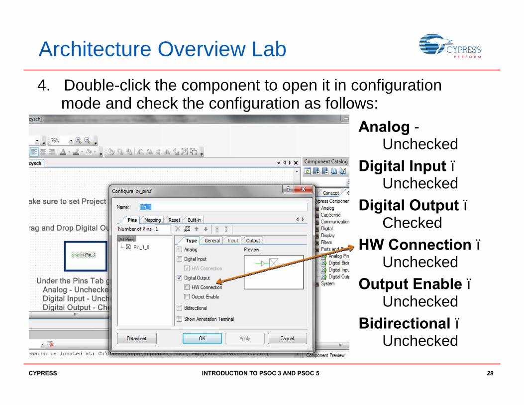
Architecture Overview Lab4. Double-click the component to open it in configuration
mode and check the configuration as follows:Analog -
UncheckedDigital Input –
UncheckedDigital Output –
CheckedHW Connection –
UncheckedOutput Enable –
UncheckedBidirectional –
Unchecked
INTRODUCTION TO PSOC 3 AND PSOC 5 30CYPRESS
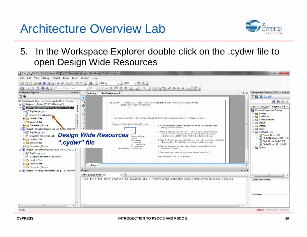
Architecture Overview Lab
5. In the Workspace Explorer double click on the .cydwr file to open Design Wide Resources
Design Wide Resources “.cydwr” file

INTRODUCTION TO PSOC 3 AND PSOC 5 31CYPRESS
Architecture Overview Lab6. Within the Design Wide Resources tab, select the Pins tab (below the chip) 7. On the right hand side of the screen, make sure that Pin 1 is set to port 6
pin 3 or P6[3]. This will set your digital output to LED4 on the PSoC Development Board.
8. Build the Project by going to the Build menu and in the drop down click “Build Overview Lab”. This will take a minute to build the project.
Build Overview Lab Confirm Pin 1 is set to port 6 pin 3 or P6[3]
Pins tab
Design Wide Resources tab
INTRODUCTION TO PSOC 3 AND PSOC 5 32CYPRESS
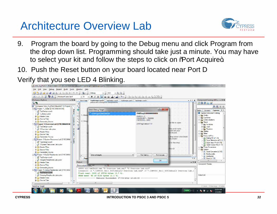
Architecture Overview Lab9. Program the board by going to the Debug menu and click Program from
the drop down list. Programming should take just a minute. You may have to select your kit and follow the steps to click on “Port Acquire”.
10. Push the Reset button on your board located near Port DVerify that you see LED 4 Blinking.

INTRODUCTION TO PSOC 3 AND PSOC 5 33CYPRESS
Architecture Overview Lab9. Program the board by going to the Debug menu and click Program from
the drop down list. Programming should take just a minute. You may have to select your kit and follow the steps to click on “Port Acquire”.
10. Push the Reset button on your board located near Port DVerify that you see LED 4 Blinking.

INTRODUCTION TO PSOC 3 AND PSOC 5 34CYPRESS
Architecture Overview Lab
This LED will blink
35
SYSTEM RESOURCES
INTRODUCTION TO PSOC 3 AND PSOC 5

INTRODUCTION TO PSOC 3 AND PSOC 5 36CYPRESS
Section Objectives
At the end of this section you will be able to§ Understand the system block diagram of PSoC 3 / PSoC 5 devices§ Understand and use the PSoC 3 / PSoC 5 System Resources, including:
• Power System• Programming and debugging• Configuration and boot process• Resets• Clocking• Memory and Mapping• DMA and PHUB• I/O• Interrupts

INTRODUCTION TO PSOC 3 AND PSOC 5 37CYPRESS
System Block Diagram

INTRODUCTION TO PSOC 3 AND PSOC 5 38CYPRESS
Power System and Supplies (no boost)Standard Power Configuration§ No boost pump§ Vdda Vddd >= Vddio0/1/2/3§ Vdda = 1.8 – 5.5V
Supply Rules and Usage§ Vdda: Must be highest voltage in system.
Supplies analog high voltage domain and core regulator§ Vddd: Supplies digital system core regulators§ Vcca: Output of the analog core regulator.
External 1.1uF capacitance to ground is required.§ Vccd: Output of the digital core regulator.
External 1.1uF capacitance to ground is required. Both Vccd pins must be tied together on the PCB and share the 1.1uF capacitance to ground§ Vddio0/1/2/3: Independent I/O supplies. May be
any voltage in the range of 1.8V to Vdda
INTRODUCTION TO PSOC 3 AND PSOC 5 39CYPRESS
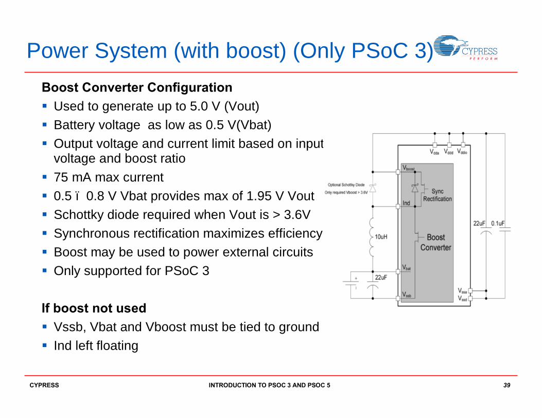
Power System (with boost) (Only PSoC 3)Boost Converter Configuration§ Used to generate up to 5.0 V (Vout)§ Battery voltage as low as 0.5 V(Vbat)§ Output voltage and current limit based on input
voltage and boost ratio§ 75 mA max current§ 0.5 – 0.8 V Vbat provides max of 1.95 V Vout§ Schottky diode required when Vout is > 3.6V§ Synchronous rectification maximizes efficiency § Boost may be used to power external circuits§ Only supported for PSoC 3
If boost not used§ Vssb, Vbat and Vboost must be tied to ground§ Ind left floating

INTRODUCTION TO PSOC 3 AND PSOC 5 40CYPRESS
Programming and Debug Interfaces
JTAG§ Legacy 4-wire Interface§ Supports all programming and debug features
Serial Wire Debug (SWD)§ Standard 2-wire interface for all CY tools and kits§ Supports all programming and debug features wth
same performance of JTAG§ Default debug interface in PSoC Creator

INTRODUCTION TO PSOC 3 AND PSOC 5 41CYPRESS
Programming and General Features
Flash operations§ Erase all§ Erase block – 256 blocks per device, independent of Flash size§ Program block§ Set block security§ Unprotected – No protection§ Factory Upgrade – Prevents external read§ Field Upgrade – Prevents external read and write§ Full Protection – Prevents external read and write as well as internal
write
General Features available through JTAG/SWD§ I/O boundary scan through JTAG interface§ Enable/Disable JTAG and SWD interfaces§ On Chip Debug features enabled/disabled by firmware

INTRODUCTION TO PSOC 3 AND PSOC 5 42CYPRESS
Reset Sources
§ PPOR – Power on Reset§ XRES – External Reset§ PRES – Under Voltage on external supplies Vddd, Vdda
(Precise Low Voltage Reset)§ PRES – Under Voltage on internal supplies Vccd, Vcca§ AHVI – Over Voltage on Vdda (Analog High Voltage
Interrupt)§ HRES – Hibernate mode under voltage detect§ SRES – User software and/or hardware generated reset§WRES – Watchdog Timer reset
§ JTAG or SWD interface generated reset

INTRODUCTION TO PSOC 3 AND PSOC 5 43CYPRESS
Clocking Sources§ Internal Main Oscillator (PSoC 3): 3-62 MHz (+/-1% at 3 MHz; +/-7% at 62 MHz)§ Internal Main Oscillator (PSoC 5): 3-74 MHz (+/-1% at 3 MHz; +/-7% at 74 MHz)§ PLL Output: 12.67 MHz (can not use 32 KHz crystal)§ External clock crystal input: 4-33 MHz§ External clock oscillator inputs: 0-33 MHz§ Clock doubler output: 12-48 MHz§ Internal Low speed Oscillator: 1 kHz, 33 kHz and 100 kHz
§ External 32 kHz crystal input for RTC

INTRODUCTION TO PSOC 3 AND PSOC 5 44CYPRESS
Clock Distribution
Clock Dividers§ 16-bit dividers§ 8 clock source inputs§ 8 digital domain clock dividers§ 4 analog domain clock dividers§ Provide skew control to reduce
digital switching noise§ 1 CPU divider
UDB’s can be used to create additional digital clocks

INTRODUCTION TO PSOC 3 AND PSOC 5 45CYPRESS
System Clock Setup
Easy to configure clock options using graphical configuration tool

INTRODUCTION TO PSOC 3 AND PSOC 5 46CYPRESS
Clock Management
Clocks allocated to dividers in clock treeClocks have software APIs to dynamically change frequency
Note: Reuse existing clocks to preserve resources
Double click clock to see component window

INTRODUCTION TO PSOC 3 AND PSOC 5 47CYPRESS
Clock Distribution
EMIF Supports:§ Sync SRAM§ Async SRAM§ Cellular RAM§ NOR Flash
EMIF Usage:§ Data only§ 8- or 16-bit data bus§ 8-, 16- or 24-bit address bus§ Max throughput 11-16 MHz
depending on configuration details

INTRODUCTION TO PSOC 3 AND PSOC 5 48CYPRESS
Flash
Flash Blocks§ 256 blocks in all devices – 64 KB flash has 256-byte block size§ Each block may be set to 1 of 4 protection levels of increasing security
• Unprotected – Allows internal and external reads and writes• Factory Upgrade – Prevents external read• Field Upgrade – Prevents external read and write• Full Protection – Prevents external read and write as well as internal write
§ Flash is erased and programmed in block units
Specs§ Code executes out of Flash§ Flash-writes block CPU unless executing from cache§ 20 year minimum retention§ 10 K minimum endurance§ 15 ms block erase + write time

INTRODUCTION TO PSOC 3 AND PSOC 5 49CYPRESS
Error Correcting Code (ECC)ECC = Flash Memory Error Correction § Required for some high reliability designs (e.g. automotive and medical)§ Detects and corrects 1 bit of error per 8 bits§ Detects but does not correct 2 bits of error§ Correction is automatic; interrupt and flag bit are set§ 1 byte of ECC data for each 8 bytes of Flash data (1 row)§ 64 KB device includes + 8 KB of ECC memory for 72 KB total8 KB is used for configuration data storage if ECC not used (default)§ ECC memory is mapped into contiguous region in peripheral space§ ECC memory may also hold user data§ Code cannot execute out of ECC memory

INTRODUCTION TO PSOC 3 AND PSOC 5 50CYPRESS
EEPROM2 KB of EEPROM are providedCode cannot execute out of EEPROM
EEPROM Specs:§ EEPROM writes do not block CPU execution§ 20 year minimum retention§ 100K minimum endurance§ 2 ms single byte erase + write time
• Supports single byte erase and writes (read / modify / write row)• May erase or write up to 16 consecutive bytes (1 row) at the same time
INTRODUCTION TO PSOC 3 AND PSOC 5 51CYPRESS
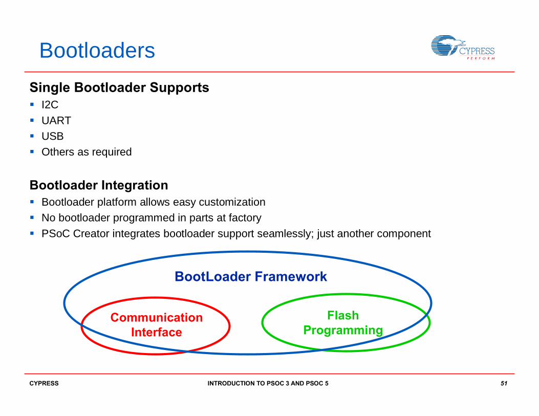
BootloadersSingle Bootloader Supports§ I2C§ UART§ USB§ Others as required
Bootloader Integration§ Bootloader platform allows easy customization§ No bootloader programmed in parts at factory§ PSoC Creator integrates bootloader support seamlessly; just another component
BootLoader Framework
Communication Interface
Flash Programming

INTRODUCTION TO PSOC 3 AND PSOC 5 52CYPRESS
Direct Memory Access (DMA)§ 24 hardware channels
§ 8 priority levels with minimum bandwidth guarantees
§ 128 Transaction Descriptors (TD) tell channel what to do• 2kB of dedicated SRAM holds all TD data
§ Multiple channels or TDs may be chained or nested
§ Configurable burst size
§ DMA between peripherals on same spoke limited to 1-byte burst length

INTRODUCTION TO PSOC 3 AND PSOC 5 53CYPRESS
GPIO - I/O Digital Features
Independent supply rails§ Each quadrant of device has
separate Vddio supply§ GPIO Vddio must be <=Vdda
Logic level maximum current§ 8 mA sink § 4 mA source
Pin maximum current§ ~25 mA sink§ ~25 mA source

INTRODUCTION TO PSOC 3 AND PSOC 5 54CYPRESS
GPIO - I/O Digital Features

INTRODUCTION TO PSOC 3 AND PSOC 5 55CYPRESS
GPIO - Interrupts
Each GPIO port has:§ Port Interrupt Control Unit (PICU)§ Dedicated Interrupt vector
Interrupt on:§ Rising edge§ Falling dege§ Any edge
Status Rgister§ Latches which pin triggered interrupt§ Available for firmware read§ Read clear

INTRODUCTION TO PSOC 3 AND PSOC 5 56CYPRESS
GPIO - I/O Analog Features§ All pins inputs and outputs§ Supports two independent analog
connections at each pin§ CapSense Touch Sensing§ LCD char/segment drive§ Hardware controlled analog mux at
pin§ Some pins have additional routing
features:• OpAmps• High Current DAC mode

INTRODUCTION TO PSOC 3 AND PSOC 5 57CYPRESS
SIO (Special I/O) FeaturesSame as GPIO with exceptions:§ 5.5 V tolerant at all Vdda levels
• Hot Swap• Overvoltage tolerance
§ Configurable drive and sense voltage levels
• Basic DAC output• High Speed CMP input
§ Logic level max current• 25 mA sink• 4 mA source
§ Pin max current• ~50 mA sink• ~25 mA source
§ No Analog§ No LCD char/segment drive§ No CapSense touch sensing
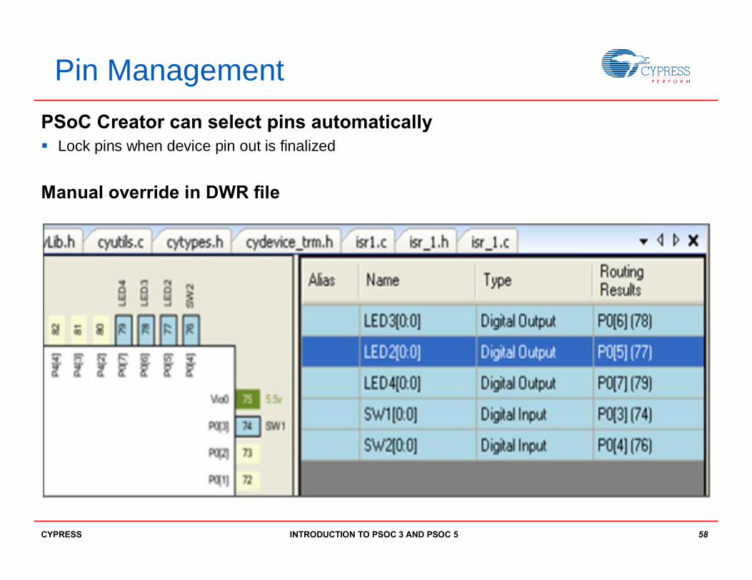
INTRODUCTION TO PSOC 3 AND PSOC 5 58CYPRESS
Pin ManagementPSoC Creator can select pins automatically§ Lock pins when device pin out is finalized
Manual override in DWR file

INTRODUCTION TO PSOC 3 AND PSOC 5 59CYPRESS
InterruptsInterrupt Controller§ 32 interrupt vectors § Dynamically adjustable vector
addresses§ 8 priority levels§ Each vector supports one of these
sources• Fixed function DMA, DSI (UDB)
route
PSoC 8051§ 32 interrupt vectors vs. standard 8051
is five
ARM Cortex-M3§ 32 interrupts + 15 exceptions§ Tail chaining

INTRODUCTION TO PSOC 3 AND PSOC 5 60CYPRESS
Interrupt ComponentGUI-based Configuration
APIisr_1_Start() – Configures and enables the interrupt. Typically the only API required
to be called
Advanced APIs§ isr_1_SetVector() – Dynamically change vector address§ isr_1_SetPriority() – Dynamically change vector priority§ isr_1_GetPriority() – Read current priority§ isr_1_Enable() – Enable interrupt vector§ isr_1_GetState() – Return current state of interrupt vector enable§ isr_1_Disable() – Disable interrupt vector§ isr_1_SetPending() – Force a pending interrupt§ isr_1_ClearPending() – Clear a pending interrupt
Double click clock to see component window

INTRODUCTION TO PSOC 3 AND PSOC 5 61CYPRESS
ReviewYou should now be able to:§ Understand the system block diagram of PSoC 3 / PSoC 5 devices§ Understand and use the PSoC 3 / PSoC 5 System Resources,
including:• Power system• Programming and debugging• Configuration and boot process• Resets• Clocking • Memory and Mapping• DMA and PHUB• I/O• Interrupts

62
SYSTEM RESOURCES LABINTRODUCTION TO PSOC 3 AND PSOC 5

INTRODUCTION TO PSOC 3 AND PSOC 5 63CYPRESS
System Resources Lab
Lab Objective§ To convert an output from the potentiometer into a digital
number using the ADC§ To display the digital number on the LCD Screen on PSoC
Development Kit

INTRODUCTION TO PSOC 3 AND PSOC 5 64CYPRESS
System Resources Lab
Instructions:1.Open LAB 22.Place the Analog Pin from Component Catalog as shown
here in the adjacent box3.Place the Delta Sigma ADC in the box as shown below.4.Double-click on the component to open it in the configuration mode and
make the following changes:Set Properties to:
Conversion Mode: 1-Multi Sample
Input Mode: Single
Resolution: 12-Bits Input Range: Vssa to Vdda
Conversion Rate: 1000 SPS Buffer Gain: 1
Clock Frequency: 131 kHz (Calculated value)
Buffer Mode: Rail to Rail

INTRODUCTION TO PSOC 3 AND PSOC 5 65CYPRESS
System Resources Lab5. Use the wire tool found on the left side of the worksheet (shown in slide
23) to connect Pin 1 to the ADC input. To use the wire tool hover over the connections until an ‘X’ appears, then click to make the connection.
6. Your final schematic should look like this when complete

INTRODUCTION TO PSOC 3 AND PSOC 5 66CYPRESS
System Resources Lab7. In the Workspace Explorer double click on the .cydwr file to open
Design wide Resources (as explained in Overview lab)8. In the Design wide Resources tab locate the section for pins on the right9. Connect the LCD to Port 2 by assigning LCDPort[6:0] to P2[6:0].
Connect Pin 1 to the potentiometer (Port 6, Pin 5) by assigning Pin_1 to P6(5).
Confirm LCD is set to Port 2 or LCDPort [6:0] to P2[6:0]Pin 1 is set to P6[3]

INTRODUCTION TO PSOC 3 AND PSOC 5 67CYPRESS
System Resources Lab
10. Build the project by going to the Build menu selecting Build System Resources Lab. This will take some time to build the project.
11. Program the board by going to the Debug menu and in the drop down click Program
12. Push the Reset button on your board located near Port D
Verify: When you turn the POT you should see the ADC values change
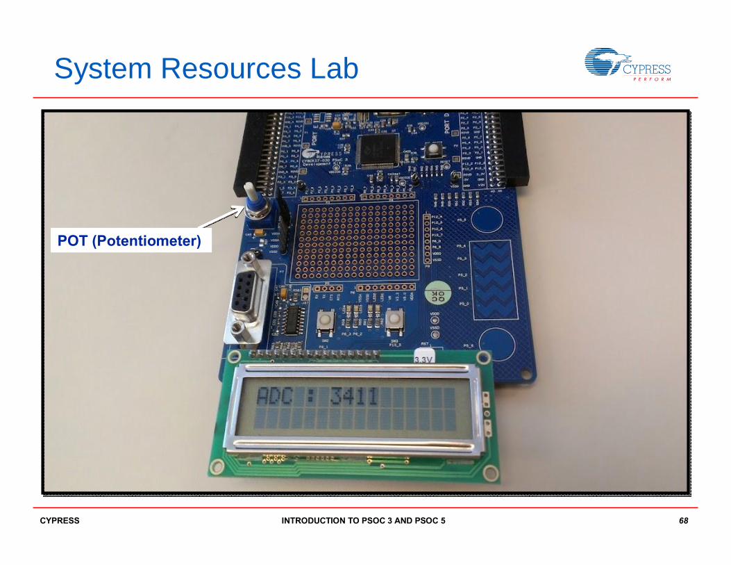
INTRODUCTION TO PSOC 3 AND PSOC 5 68CYPRESS
System Resources Lab
POT (Potentiometer)

69
DIGITAL PERIPHERALSINTRODUCTION TO PSOC 3 AND PSOC 5

INTRODUCTION TO PSOC 3 AND PSOC 5 70CYPRESS
Section Objectives
At the end of this section you should be able to:§ Understand Universal Digital Blocks (UDBs) in PSoC 3 /
PSoC 5§ Use and implement digital peripherals with PSoC Creator
INTRODUCTION TO PSOC 3 AND PSOC 5 71CYPRESS
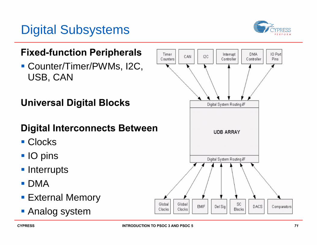
Digital Subsystems
Fixed-function Peripherals§ Counter/Timer/PWMs, I2C,
USB, CAN
Universal Digital Blocks
Digital Interconnects Between§ Clocks§ IO pins§ Interrupts§ DMA§ External Memory§ Analog system

INTRODUCTION TO PSOC 3 AND PSOC 5 72CYPRESS
UDB Array

INTRODUCTION TO PSOC 3 AND PSOC 5 73CYPRESS
Digital Signal Interconnects (DSI)
Routing Example:§ Single UDB Pair§ 7000 DSI registers
INTRODUCTION TO PSOC 3 AND PSOC 5 74CYPRESS
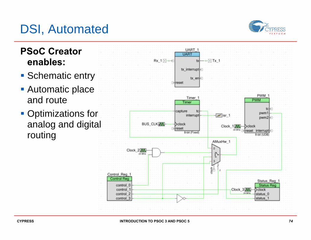
DSI, Automated
PSoC Creator enables:§ Schematic entry§ Automatic place
and route§ Optimizations for
analog and digital routing

INTRODUCTION TO PSOC 3 AND PSOC 5 75CYPRESS
UDB Block Diagram

INTRODUCTION TO PSOC 3 AND PSOC 5 76CYPRESS
Digital Peripherals
Sample of Digital Peripherals:§ Counter§ Timer§ PWM§ PRS§ I2C§ USB§ UART§ SPI§ CAN§ Char/Segment LCD Drive

INTRODUCTION TO PSOC 3 AND PSOC 5 77CYPRESS
CounterFixed/UDB Counters:§ General-Purpose counter§ Continuous, reload on reset,
terminal count, or one shot mode§ Compare options: < <= > >= =§ Enable, reset, capture inputs§ Compare, TC, interrupt outputs§ Interrupts on various events
Fixed-Function Counters:§ 4 Available§ 8- or 16-bit§ Down counter only§ Single capture registerUDB-Based:§ 8-, 16-, 24- or 32-bit§ Many options:
• Enable, count, capture, compare
• 4-deep capture FIFO
Double Click Counter to configure
INTRODUCTION TO PSOC 3 AND PSOC 5 78CYPRESS
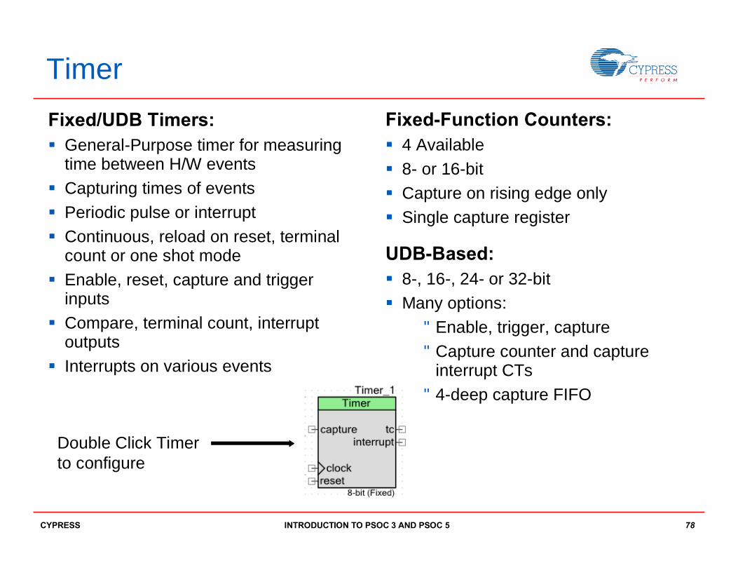
TimerFixed/UDB Timers:§ General-Purpose timer for measuring
time between H/W events§ Capturing times of events§ Periodic pulse or interrupt§ Continuous, reload on reset, terminal
count or one shot mode§ Enable, reset, capture and trigger
inputs§ Compare, terminal count, interrupt
outputs§ Interrupts on various events
Fixed-Function Counters:§ 4 Available§ 8- or 16-bit§ Capture on rising edge only§ Single capture register
UDB-Based:§ 8-, 16-, 24- or 32-bit§ Many options:
• Enable, trigger, capture• Capture counter and capture
interrupt CTs• 4-deep capture FIFO
Double Click Timer to configure
INTRODUCTION TO PSOC 3 AND PSOC 5 79CYPRESS
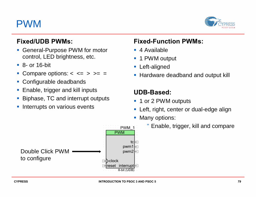
PWMFixed/UDB PWMs:§ General-Purpose PWM for motor
control, LED brightness, etc.§ 8- or 16-bit§ Compare options: < <= > >= =§ Configurable deadbands§ Enable, trigger and kill inputs§ Biphase, TC and interrupt outputs§ Interrupts on various events
Fixed-Function PWMs:§ 4 Available§ 1 PWM output§ Left-aligned§ Hardware deadband and output kill
UDB-Based:§ 1 or 2 PWM outputs§ Left, right, center or dual-edge align§ Many options:
• Enable, trigger, kill and compare
Double Click PWM to configure
INTRODUCTION TO PSOC 3 AND PSOC 5 80CYPRESS
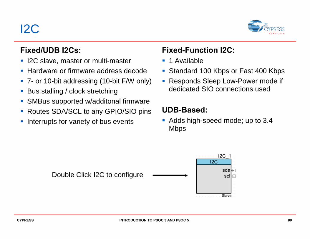
I2CFixed/UDB I2Cs:§ I2C slave, master or multi-master§ Hardware or firmware address decode§ 7- or 10-bit addressing (10-bit F/W only)§ Bus stalling / clock stretching§ SMBus supported w/additonal firmware§ Routes SDA/SCL to any GPIO/SIO pins§ Interrupts for variety of bus events
Fixed-Function I2C:§ 1 Available§ Standard 100 Kbps or Fast 400 Kbps§ Responds Sleep Low-Power mode if
dedicated SIO connections used
UDB-Based:§ Adds high-speed mode; up to 3.4
Mbps
Double Click I2C to configure

INTRODUCTION TO PSOC 3 AND PSOC 5 81CYPRESS
Pseudo Random SequencerPseudo Random Sequencer (PRS)Specs:§ 2- to 64-bit sequence length§ Serial output bit stream§ Continuous or single step run modes§ Standard or custom polynomial§ Standard or custom seed value§ Enable input provides synchronized
operation with other components§ Computed pseudo-random number can
be read directly from the linear feedback shift register (LFSR)
Double Click PRS to configure

INTRODUCTION TO PSOC 3 AND PSOC 5 82CYPRESS
USBSpecs:§ Fixed-function, USB 2.0 Full Speed (12
Mbps) peripheral§ 8 unidirectional endpoints§ Shared 512 byte buffer§ Transfer Types: Control, Interrupt, Bulk,
Isochronous§ DMA access / capable§ Wake from sleep
Double Click USB to configure

INTRODUCTION TO PSOC 3 AND PSOC 5 83CYPRESS
UARTSpecs:§ Full-Duplex, Tx only and Rx only§ 5- to 9-data bits§ 110- to 921600-bps or arbitrary up to 4
Mbps§ Rx and Tx buffers 1- to 255-bytes§ Framing, Parity and Overrun error
detection§ 9-bit address mode with hardware
address detection§ Optional Tx enable for RS-485
Double Click UART to configure

INTRODUCTION TO PSOC 3 AND PSOC 5 84CYPRESS
SPISpecs:§ Master or Slave§ Data rates to 33 Mbps§ 2- to 16-bit data width§ 4 SPI modes§ LSB or MSB first§ 1- to 255-byte Rx and Tx buffers§ Hardware Slave Select generation§ Supports 3-wire mode
Double Click SPI to configure

INTRODUCTION TO PSOC 3 AND PSOC 5 85CYPRESS
CANSpecs:§ CAN 2.0A/B spec. compliant
• Remote Transmission Request (RTR) support• Programmable bit rate up to 1Mbps• External CAN PHY connects to any GPIO
§ Transmit path:• 8 transmit message buffers• Programmable priority for each
§ Receive path:• 16 receive message buffers• 16 acceptance filters/masks• DeviceNet addressing support• Option to link multiple receive buffers to/from
a hardware FIFO
Double Click CAN to configure

INTRODUCTION TO PSOC 3 AND PSOC 5 86CYPRESS
LCD DriveSpecs:§ Drives up to 736-segments (16-commons/46-front
plane)§ Up to 62 total LCD drive pins; commons and
segment lines mapped to any GPIO§ High multiplex ratio of up to 1/16 for max 16
segments§ Type A (standard) and Type B (low power)
waveforms supported§ Wide operating voltage range supported (2V to
5.2V) for LCD panels§ Static, ½, 1/3, ¼, 1/5 bias voltage levels§ Vias voltage generation using dedicated DAC, and
internal resistor leader§ Up to 128 levels of software controlled contrast§ Ability to move display data from memory to LCD
via DMA§ Adjustable LCD refresh rate from 10 Hz to 150 Hz
Double Click LCD to configure

INTRODUCTION TO PSOC 3 AND PSOC 5 87CYPRESS
Review
You should now be able to:§ Understand Universal Digital Blocks (UDBs) in PSoC 3 /
PSoC 5§ Use and implement digital peripherals with PSoC Creator

88
DIGITAL PERIPHERALS LAB
INTRODUCTION TO PSOC 3 AND PSOC 5

INTRODUCTION TO PSOC 3 AND PSOC 5 89CYPRESS
Lab Objective§ To use two PWMs to change the duty cycle on the LED to
make it a “Breathing” LED using your PSoC Development kit for this.
Digital Peripherals Lab

INTRODUCTION TO PSOC 3 AND PSOC 5 90CYPRESS
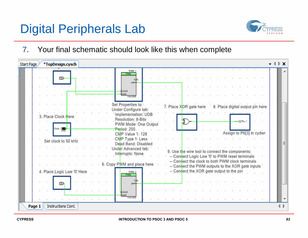
Instructions:1.Open LAB 3 from the flash drive2.Find the following components from the Component catalog on the right
side of the screen and place them in the boxes given on the “Top Design.cysch” schematic file. These are shown below:
Digital Peripherals Lab
Logic Low ‘0’ XOR Gate
Clock Digital Output Pin
PWM

INTRODUCTION TO PSOC 3 AND PSOC 5 91CYPRESS
3. Place the components inside the right boxes shown on the schematic file
4. Double click on the clock component to open it in configuration mode and set it to 50 kHz
5. Double click on the PWM component to open it in configuration mode and make the following changes to its properties
Set Properties to:
6. Copy the first PWM from the top box into the bottom box and change the “Period” to 254
Implementation: UDB CMP Value 1: 128Resolution: 8-Bits CMP Type 1: LessPWM mode: One Output Dead Band : DisabledPeriod: 255 Under Advanced tab:
Interrupts: None
Digital Peripherals Lab

INTRODUCTION TO PSOC 3 AND PSOC 5 92CYPRESS
6. Use the wire tool to make the following connection between the components:§ Connect Logic Low ‘0’ to PWM reset terminals§ Connect the clock to both PWM clock terminals§ Connect the PWM outputs to the XOR gate inputs§ Connect the XOR gate output to the pin.
Digital Peripherals Lab
INTRODUCTION TO PSOC 3 AND PSOC 5 93CYPRESS
7. Your final schematic should look like this when complete
Digital Peripherals Lab

INTRODUCTION TO PSOC 3 AND PSOC 5 94CYPRESS
8. In the Workspace Explorer double click on the .cydwr file to open Design wide Resources (as explained in Overview lab)
9. In the Design wide Resources tab locate the section for pins on the right10. Configure the I/O so that Pin 1 is connected to Port 6 pin 3 or P6[3].
Digital Peripherals Lab
Confirm Pin 1 is connected to Port 6 pin 3 or P6[3]
INTRODUCTION TO PSOC 3 AND PSOC 5 95CYPRESS
11. Build the project by going to the Build menu selecting Build Digital Peripherals Lab or pressing Shift + F6. This will take some time to build the project.
12.Program the board by going to the Debug menu and in the drop down click Program
13.Push the Reset button on your board located near Port D
Verify: LED 4 is seen “Breathing”.
Digital Peripherals Lab
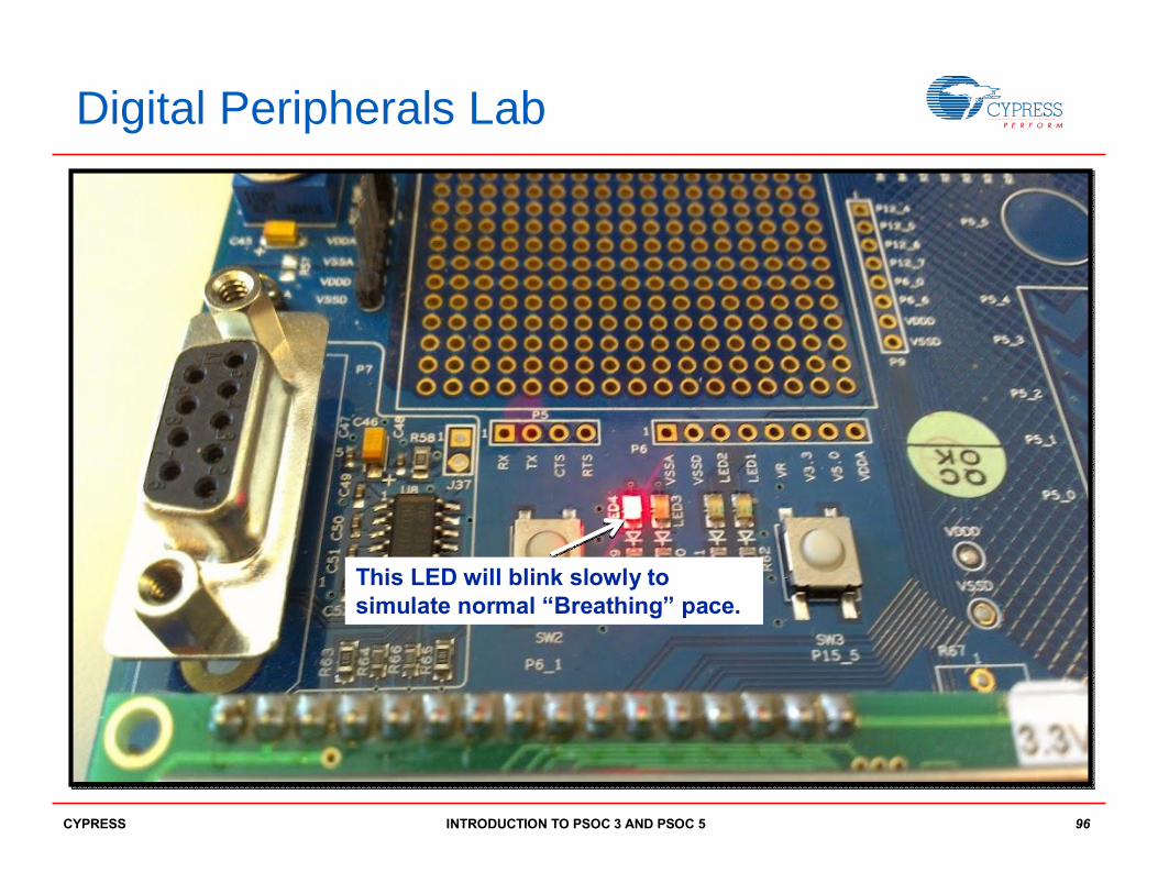
INTRODUCTION TO PSOC 3 AND PSOC 5 96CYPRESS
Digital Peripherals Lab
This LED will blink slowly to simulate normal “Breathing” pace.

97
ANALOG PERIPHERALSINTRODUCTION TO PSOC 3 AND PSOC 5

INTRODUCTION TO PSOC 3 AND PSOC 5 98CYPRESS
Section Objectives
At the end of this section you will be able to§ Understand analog in PSoC 3 / PSoC 5§ Use and understand analog peripherals in PSoC Creator

INTRODUCTION TO PSOC 3 AND PSOC 5 99CYPRESS
Analog SubsystemRoutingMultiplexersComparatorsOpampsDACs (V & I)DeltaSigma ADCProgrammable Analog§ PGA§ TIA§ MixerCapSense Touch SensingDigital Filters
INTRODUCTION TO PSOC 3 AND PSOC 5 100CYPRESS
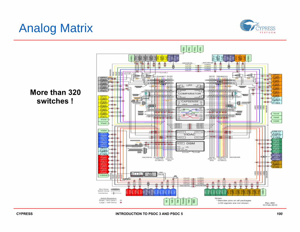
Analog Matrix
More than 320 switches !

INTRODUCTION TO PSOC 3 AND PSOC 5 101CYPRESS
Analog Matrix
PSoC Creator enables:§ Schematic Entry§ Automatic place and route§ Optimizations for analog and digital routing

INTRODUCTION TO PSOC 3 AND PSOC 5 102CYPRESS
Routing with Muxes
Analog Multiplexer Specs:§ Bi-directional§ Either single ended or differential§ Actual routing hidden from user§ May have more than one connection at a time§ Analog routing may be controlled by digital subsystem
Double Click MUX to configure

INTRODUCTION TO PSOC 3 AND PSOC 5 103CYPRESS
Analog Peripheral: Comparator
Specs:§ Up to four per device§ Speeds:
• Fast – 80 ns / 250 uA• Slow – 55 us / 6 uA
§ Accuracy:• 2 mV fast mode• Zero-adjust; Internal VDAC
§ Hysteresis:• 10 mV nominal• May be enabled or disabled

INTRODUCTION TO PSOC 3 AND PSOC 5 104CYPRESS
Analog Peripheral: Opamp
Specs:§ Up to four per device§ Speeds:
• Fast – 80 ns / 250 uA• Slow – 55 us / 6 uA
§ Accuracy:• 2 mV fast mode• Zero-adjust; Internal VDAC
§ Hysteresis:• 10 mV nominal• May be enabled or disabled
INTRODUCTION TO PSOC 3 AND PSOC 5 105CYPRESS
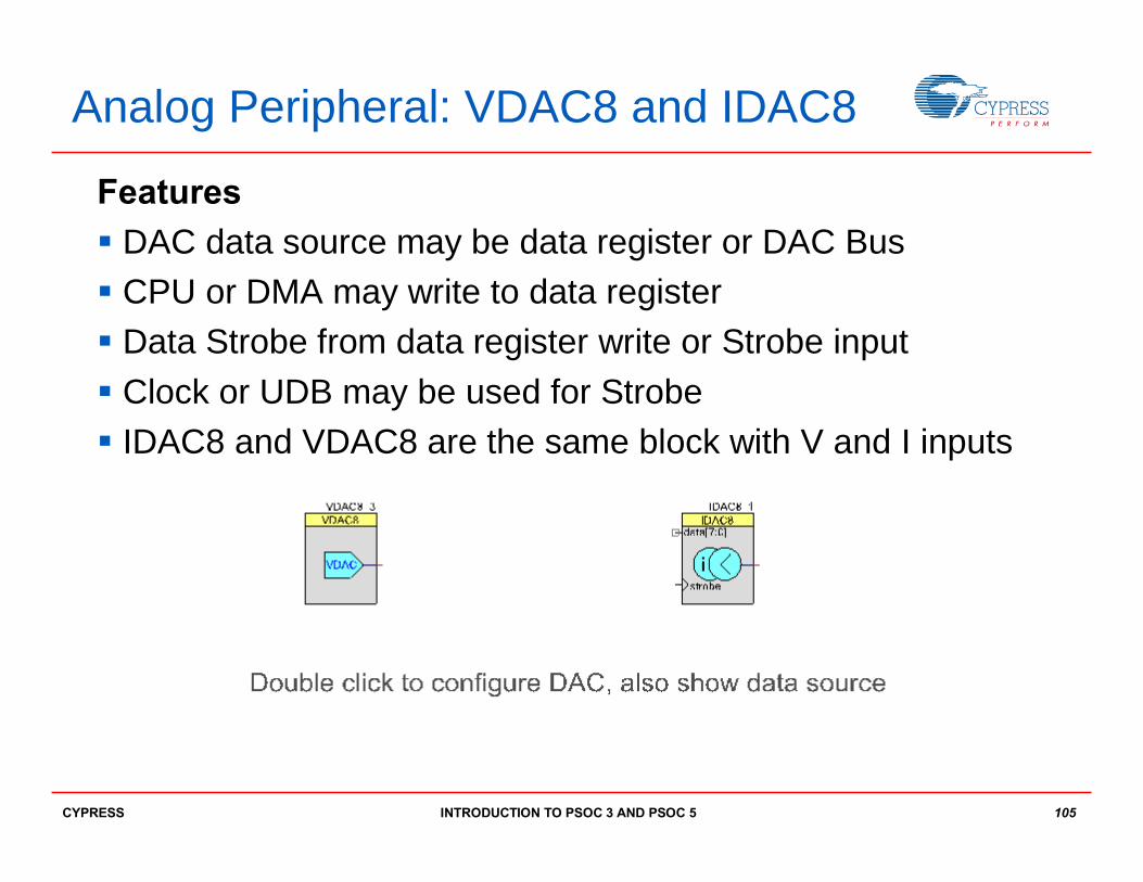
Analog Peripheral: VDAC8 and IDAC8
Features§ DAC data source may be data register or DAC Bus§ CPU or DMA may write to data register§ Data Strobe from data register write or Strobe input§ Clock or UDB may be used for Strobe§ IDAC8 and VDAC8 are the same block with V and I inputs

INTRODUCTION TO PSOC 3 AND PSOC 5 106CYPRESS
Analog Peripheral: IDAC8
Specs:§ Source or sink§ Ranges:
• 0 to 31.875 uA (125 nA/bit)• 0 to 255 uA (1 uA/bit)• 0 to 2.04 mA (8 uA/bit)
§ Power (ICC):• 100 uA max slow mode• 500 uA max fast mode

INTRODUCTION TO PSOC 3 AND PSOC 5 107CYPRESS
Analog Peripheral: VDAC8Specs:§ Ranges:
• 0 to 1.02V (4mV/bit)• 0 to 4.08V (16mV/bit)
§ Output R = ~16 k ohms (4 volt range)• Must be buffered for external use• Some internal loads don’t require
buffering§ Power (ICC):
• 100 uA max slow mode• 500 uA max fast mode
§ Speed:• 1 Msps (1V mode)• 250 ksps (4V mode)

INTRODUCTION TO PSOC 3 AND PSOC 5 108CYPRESS
Analog Peripheral: Delta Sigma ADCSpecs:§ High speed, high resolution ADC§ Selectable resolutions (8- to 20-bit)§ Several input ranges§ High-impedance input buffers
• Programmable gain (1,2,4,8)• Chopper mode for low offset• Internal reference may be
bypassed§ Single and differential input modes§ Wide range of sample rates 10 to
375K§ Multiple reference sources§ Drop, connect, and go!
INTRODUCTION TO PSOC 3 AND PSOC 5 109CYPRESS
Programmable Analog Peripherals
Specs:§ Combination of functions from PSoC1 programmable analog
catalog§ Switched-Capacitor (SC)-based analog§ Continuous Time blocks (CT)-based analog

INTRODUCTION TO PSOC 3 AND PSOC 5 110CYPRESS
Analog Peripheral: PGA
Specs:§ Programmable Gain Amplifier§ Amplify signals without
external components§ Gain: 1x to 50x§ Vin and Vref to any pin
Accuracy:§ Gain: +/- 5%§ Vos: 10 mV
INTRODUCTION TO PSOC 3 AND PSOC 5 111CYPRESS
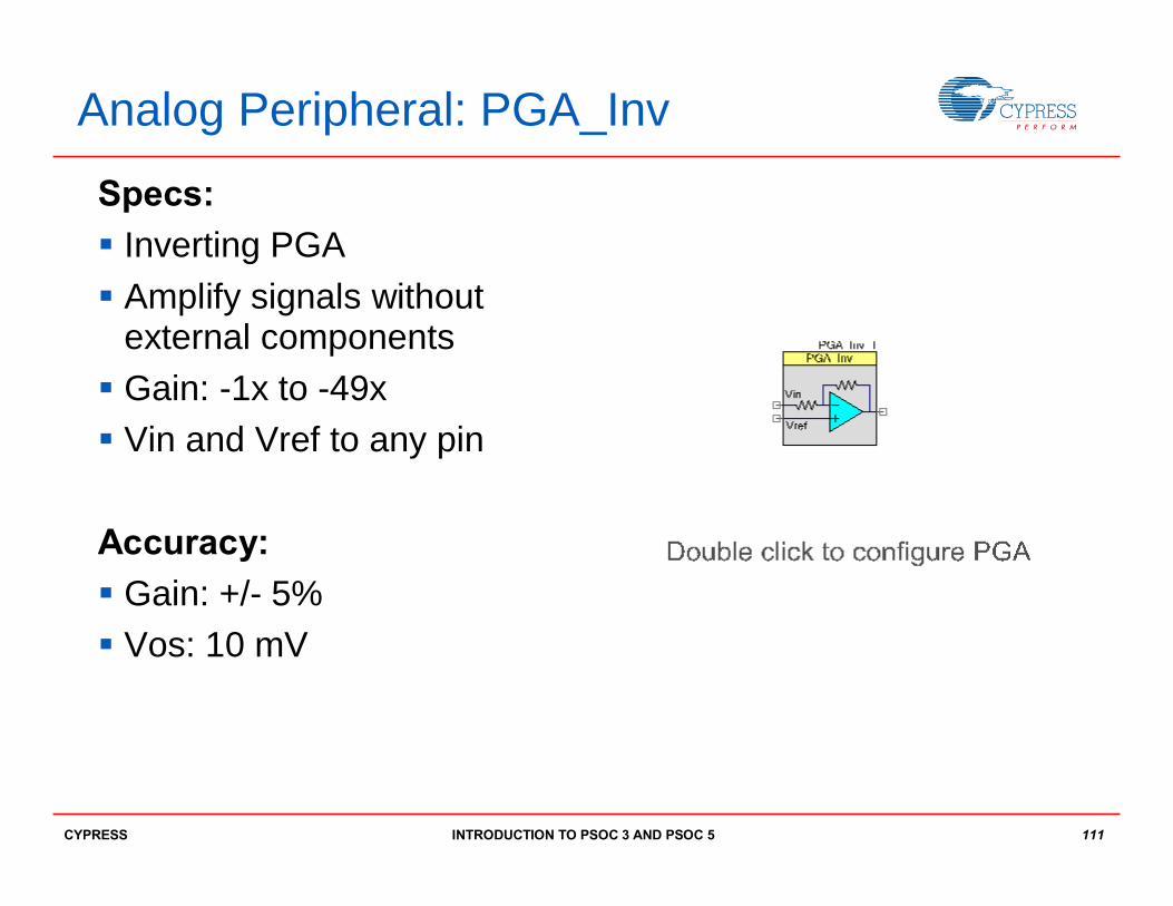
Analog Peripheral: PGA_Inv
Specs:§ Inverting PGA§ Amplify signals without
external components§ Gain: -1x to -49x§ Vin and Vref to any pin
Accuracy:§ Gain: +/- 5%§ Vos: 10 mV

INTRODUCTION TO PSOC 3 AND PSOC 5 112CYPRESS
Analog Peripheral: TIASpecs:§ Trans-Impedance Amplifier§ Conversion gain is a “resistor”
• Current IN -> Volts OUT• Vout = Vref – Iin*Rfb• Adjustable Rfb = Programmable gain (20k
to 1M)• Adjustable Cfb = Programmable bandwidth
(up to 4.7 pF)• Calibrated with on-chip IDAC (internal
resistors +/- 30%)§ Applicable to current output sensors
• Glucose meters• Photo-diodes – light meters, medium
speed IR receiver

INTRODUCTION TO PSOC 3 AND PSOC 5 113CYPRESS
Analog Peripheral: MixerSpecs:§ LO_Freq = Local Oscillator
Mixer Modes:§ Up-Mixer: Multiplier
• Clock up to 1.0 MHz• Output at LO_Freq +/- Fin• Example 200 kHz input clocked at 255 kHz
to narrowband filter at 455 kHZ
§ Down-Mixer Sampler• Clock up to 4.0 MHz• Output at Fin – LO_Freq• Example 455 clocked at 435 kHz to low-
pass filter at 25 kHz

INTRODUCTION TO PSOC 3 AND PSOC 5 114CYPRESS
Analog Peripheral: CapSense®
Specs:§ CapSense peripheral uses configuration of
existing system resources§ Two simultaneous CapSense systems possible§ CapSense Configurations
• All have similar configuration patterns• Buttons: Basic CapSense sensor with
On/Off detection• Sliders: Linear and radial with interpolated
positioning (also supports diplexing to reduce pin count)
• Touch Pads: X, Y interpolated positioning• Matrix Buttons• Proximity Sensors• Generic Sensors

INTRODUCTION TO PSOC 3 AND PSOC 5 115CYPRESS
Analog Peripheral: DFBSpecs:§ Digital Filter Block§ What it does:
• Works on digitized data from ADC or any other source• Sequentially calculate multiple filters• Removes noise and unwanted frequencies from signals• Replaces analog filters requiring external components
§ How it works:• No coding or coefficients! All handled by GUI• 24-bit filter co-processor• 128 pairs of data/coefficients
§ Setting for filters can be made for 2 channels§ Select type:
• Low Pass, Band Pass, High Pass, Notch§ Select implementation:
• FIR or IIR Biquad§ Specify sample rate§ Specify number of taps§ Select frequency parameters

INTRODUCTION TO PSOC 3 AND PSOC 5 116CYPRESS
Review
You should now be able to:§ Understand analog in PSoC 3 / PSoC 5§ Use and understand analog peripherals in PSoC Creator

117
ANALOG PERIPHERALS LAB
INTRODUCTION TO PSOC 3 AND PSOC 5

INTRODUCTION TO PSOC 3 AND PSOC 5 118CYPRESS
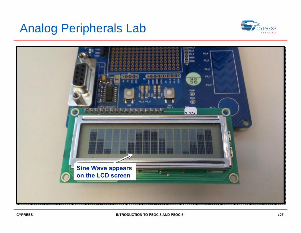
Lab Objective § To use a VDAC to convert a clock signal into an analog signal
then convert it back into digital signal using an ADC DelSig.§ To output the signal on the LCD Screen using the vertical bar
graph option using your PSoC 3 Development kit for this. § To be able to see a sine wave on the screen when the lab is
complete.
Analog Peripherals Lab

INTRODUCTION TO PSOC 3 AND PSOC 5 119CYPRESS
Instructions:1.Open LAB 4 from the flash drive and find the following components from
the Component catalog on the right side of the screen and place them in the boxes given on the “Top Design.cysch” schematic file.
2.These are shown below:
Analog Peripherals Lab
Clock ADC Del-Sig
VADC
Interrupt
INTRODUCTION TO PSOC 3 AND PSOC 5 120CYPRESS
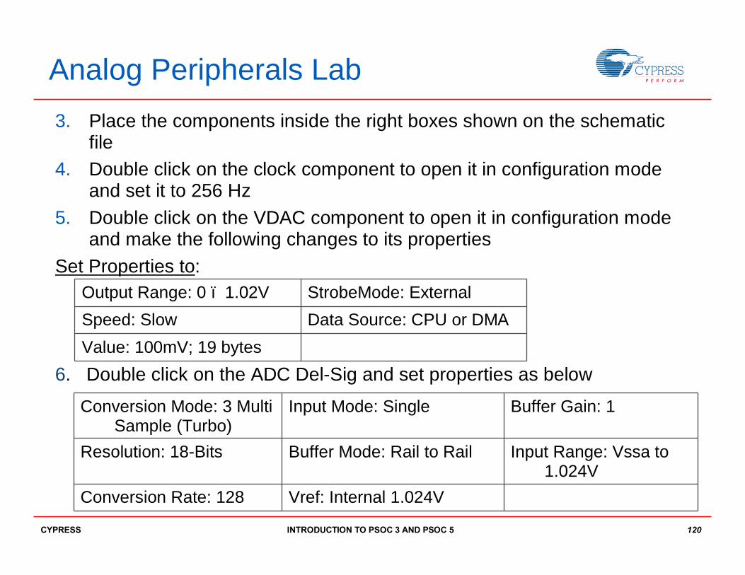
3. Place the components inside the right boxes shown on the schematic file
4. Double click on the clock component to open it in configuration mode and set it to 256 Hz
5. Double click on the VDAC component to open it in configuration mode and make the following changes to its properties
Set Properties to:
6. Double click on the ADC Del-Sig and set properties as below
Output Range: 0 – 1.02V StrobeMode: ExternalSpeed: Slow Data Source: CPU or DMAValue: 100mV; 19 bytes
Analog Peripherals Lab
Conversion Mode: 3 Multi Sample (Turbo)
Input Mode: Single Buffer Gain: 1
Resolution: 18-Bits Buffer Mode: Rail to Rail Input Range: Vssa to 1.024V
Conversion Rate: 128 Vref: Internal 1.024V

INTRODUCTION TO PSOC 3 AND PSOC 5 121CYPRESS
7. Use the wire tool to make the following connection between the components:§ Connect Clock to the strobe input of the VDAC§ Connect the Clock to the Interrupt§ Connect VDAC output to the input of the Single ended
ADC DelSig
Analog Peripherals Lab

INTRODUCTION TO PSOC 3 AND PSOC 5 122CYPRESS
8. Your final schematic should look like this when complete
Analog Peripherals Lab

INTRODUCTION TO PSOC 3 AND PSOC 5 123CYPRESS
9. In the Workspace Explorer double click on the .cydwr file to open Design wide Resources (as explained in Overview lab)
10. In the Design wide Resources tab locate the section for pins on the right11. Configure the I/O so that the LCD is connected to port 2 pins 0-6 or
P2(6:0).
Analog Peripherals Lab
Confirm LCD is connected to port 2 pins 0-6 or P2[6:0]

INTRODUCTION TO PSOC 3 AND PSOC 5 124CYPRESS
12.Build the project by going to the Build menu selecting Build Analog Peripherals Lab or pressing Shift + F6. This will take some time to build the project.
13.Program the board by going to the Debug menu and in the drop down click Program
14.Push the Reset button on your board located near Port D
Verify: You should see a sine wave moving across the LCD screen.
Analog Peripherals Lab
INTRODUCTION TO PSOC 3 AND PSOC 5 125CYPRESS
Analog Peripherals Lab
Sine Wave appears on the LCD screen