pth05000w —5-v input - texas instruments notes for technical support and further information visit...
TRANSCRIPT

For technical support and further information visit http://power.ti.com
Standard Application
Features• Up to 6-A Output Current• 5-V Input Voltage• Wide-Output Voltage Adjust
(0.9 V to 3.6 V)• Efficiencies up to 94 %• 160 W/in³ Power Density• On/Off Inhibit• Under-Voltage Lockout
6-A, 5-V Input Non-IsolatedWide-Output Adjust Power Module
Rset = Required to set the output voltage to a valuehigher than 0.9 V. See spec. table for values.
Cin = Required 330 µF capacitorCout = Optional 100 µF capacitor
• Output Current Limit• Pre-Bias Startup Capability• Over-Temperature Protection• Surface Mountable• Operating Temp: –40 to +85 °C• Safety Agency Approvals (Pending):
UL 1950, CSA 22.2 950, EN60950& VDE
VIN
Inhibit
GND GND
VOUT
RSET
1 %, 0.1 W(Required)
COUT100 µFElectrolytic(Optional)
CIN330 µF(Required)
PTH05000W(Top View)
1
4
2
3
5
SLTS201C – MAY 2003 – REVISED DECEMBER 2003
DescriptionThe PTH05000 series of non-isolated
power modules are small in size and highon performance. Using double-sided sur-face mount construction and synchronousrectification technology, these regulatorsdeliver up to 6 A of output current whileoccupying a PCB area of about half thesize of a standard postage stamp. Theyare an ideal choice for applications wherespace, performance and cost are impor-tant design constraints.
The series operates from an inputvoltage of 5 V to provide step-downpower conversion to any output voltageover the range, 0.9 V to 3.6 V. The out-put voltage of the PTH05000W is setwithin this range using a single resistor.
Operating features include an on/offinhibit, output voltage adjust (trim), anoutput current limit, and over-tempera-ture protection.
For high efficiency these parts employa synchronous rectifier output stage. Anoutput pre-bias holdoff capability ensuresthat the output will not sink current dur-ing startup.
Target applications include telecom,industrial, and general purpose circuits,including low-power dual-voltage systemsthat use a DSP, microprocessor, or ASIC.
Package options include both through-hole and surface mount configurations.
Pin ConfigurationPin Function1 GND2 Vin
3 Inhibit *4 Vo Adjust5 Vout
* Denotes negative logic:Open = Output OnGround = Output Off
NOMINAL SIZE = 0.75 in x 0.5 in(19,05 mm x 12,7 mm)
PTH05000W —5-V Input
For technical support and further information visit http://power.ti.com
Pin Descriptions
Vin: The positive input voltage power node to the mod-ule, which is referenced to common GND.
Vout: The regulated positive power output with respectto the GND node.
GND: This is the common ground connection for the‘Vin’ and ‘Vout’ power connections. It is also the 0 VDCreference for the ‘Inhibit’ and ‘Vo Adjust’ control input.
Inhibit: The Inhibit pin is an open-collector/drain negativelogic input that is referenced to GND. Applying a low-level ground signal to this input disables the module’soutput and turns off the output voltage. When the Inhibitcontrol is active, the input current drawn by the regulatoris significantly reduced. If the Inhibit pin is left open-circuit, the module will produce an output whenever avalid input source is applied.
Vo Adjust: A 0.1 W 1 % resistor must be directly connectedbetween this pin and the GND pin to set the output voltageto a value higher than 0.9 V. The temperature stabilityof the resistor should be 100 ppm/°C (or better). The setpoint range for the output voltage is from 0.9 V to 3.6 V.The resistor required for a given output voltage may becalculated from the following formula. If left open circuit,the output voltage will default to its lowest value. Forfurther information on output voltage adjustment, consultthe related application note.
Rset = 10 kΩ · 0.891 V – 3.24 kΩ Vout – 0.9 V
The specification table gives the preferred resistor valuesfor a number of standard output voltages.
Ordering Information
Package Options (PTH05000x) (1)
Code Description Pkg Ref. (2)
AH Horiz. T/H (EUS)AS SMD, Standard (3) (EUT)
Output Voltage (PTH05000xx)Code Voltage
W 0.9 V – 3.6 V (Adjust)
Notes: (1) Add “T” to end of part number for tape and reel on SMD packages only.(2) Reference the applicable package reference drawing for the dimensions and PC board layout(3) “Standard” option specifies 63/37, Sn/Pb pin solder material.
6-A, 5-V Input Non-IsolatedWide-Output Adjust Power Module SLTS201C – MAY 2003 – REVISED DECEMBER 2003
PTH05000W —5-V Input

For technical support and further information visit http://power.ti.com
Environmental & Absolute Maximum RatingsCharacteristics Symbols Conditions Min Typ Max Units
Operating Temperature Range Ta Over Vin Range –40 (i) — +85 °CSolder Reflow Temperature Treflow Surface temperature of module body or pins 235 (ii) °CStorage Temperature Ts — –40 — +125 °COver Temperature Protection OTP IC junction temperature — 150 — °CMechanical Shock Per Mil-STD-883D, Method 2002.3 — 500 — G’s1 msec, ½ sine, mountedMechanical Vibration Mil-STD-883D, Method 2007.2 — 20 — G’s20-2000 HzWeight — — 2 — gramsFlammability — Meets UL 94V-O
Notes: (i) For operation below 0 °C the external capacitors must have stable characteristics. Use either a low ESR tantalum, Os-con, or ceramic capacitor.(ii) During reflow of SMD package version do not elevate peak temperature of the module, pins or internal components above the stated maximum.
6-A, 5-V Input Non-IsolatedWide-Output Adjust Power Module SLTS201C – MAY 2003 – REVISED DECEMBER 2003
PTH05000W —5-V Input
Electrical Specifications Unless otherwise stated, Ta =25 °C, Vin =5 V, Vo =3.3 V, Cin =330 µF, Cout =0 µF, and Io =Io(max)
PTH05000WCharacteristics Symbols Conditions Min Typ Max Units
Output Current Io 0.9 V ≤ Vo ≤3.6 V, Ta =25 °C, natural convection 0 — 6 (1) ATa =60 °C, 200LFM 0 — 5.25 (1)
Input Voltage Range Vin Over Io range 4.5 — 5.5 VSet-Point Voltage Tolerance Vo tol — — ±2 (2) %Vo
Temperature Variation ∆Regtemp –40 °C <Ta < +85 °C — ±0.5 — %Vo
Line Regulation ∆Regline Over Vin range — ±5 — mVLoad Regulation ∆Regload Over Io range — ±5 — mVTotal Output Variation ∆Regtot Includes set-point, line, load, — — ±3 (2) %Vo–40 °C ≤ Ta ≤ +85 °CEfficiency η Vin =5 V, Io =4 A RSET = 475 Ω Vo = 3.3 V — 92 —
RSET = 2.32 kΩ Vo = 2.5 V — 90 —RSET = 4.87 kΩ Vo = 2.0 V — 88 —RSET = 6.65 kΩ Vo = 1.8 V — 87 — %RSET = 11.5 kΩ Vo = 1.5 V — 84 —RSET = 26.1 kΩ Vo = 1.2 V — 82 —RSET = 84.5 kΩ Vo = 1.0 V — 79 —
Vo Ripple (pk-pk) Vr 20 MHz bandwidth Vo ≥3.3 V — 30 — mVppVo ≤2.5 V — 25 —Transient Response 1 A/µs load step, 50 to 100 % Iomax,
Vo =1.8 V, Cout =100 µFttr Recovery time — 70 — µSec∆Vtr Vo over/undershoot — 100 — mV
Current Limit Ilim ∆Vo = –50 mV — 13 — AUnder-Voltage Lockout UVLO Vin increasing — 3.8 4.3 VVin decreasing 3.4 3.5 —Inhibit Control (pin 3) Referenced to GND Input High Voltage VIH Vin –0.5 — Open (3) V Input Low Voltage VIL –0.2 — 0.8 Input Low Current IIL Pin 3 to GND — –10 — µAStandby Input Current Iin standby pins 1 & 3 connected — 1 — mASwitching Frequency ƒs Over Vin and Io ranges — 700 — kHzExternal Input Capacitance Cin 330 (4) — — µFExternal Output Capacitance Cout Capacitance value non-ceramic 0 100 (5) 1,000 (6) µFceramic 0 — 300
Equiv. series resistance (non-ceramic) 4 (7) — — mΩReliability MTBF Per Bellcore TR-332 28 — — 106 Hrs50 % stress, Ta =40 °C, ground benign
Notes: (1) See SOA curves or consult factory for appropriate derating.(2) The set-point voltage tolerance is affected by the tolerance and stability ofRSET. The stated limit is unconditionally met if RSET has a tolerance of 1 %
with 100 ppm/°C or better temperature stability.(3) The Inhibit control (pin 3) has an internal pull-up to Vin, and if left open-circuit the module will operate when input power is applied. A small low-
leakage (<100 nA) MOSFET is recommended to control this input. See application notes for more information.(4) The regulator requires a minimum of 330 µF input capacitor with a minimum 300 mArms ripple current rating. For further information, consult the
related application note on Capacitor Recommendations.(5) An external output capacitor is not required for basic operation. Adding 100 µF of distributed capacitance at the load will improve the transient response.(6) This is the calculated maximum. The minimum ESR limitation will often result in a lower value. Consult the application notes for further guidance.(7) This is the typical ESR for all the electrolytic (non-ceramic) output capacitance. Use 7 mΩ as the minimum when using max-ESR values to calculate.
For technical support and further information visit http://power.ti.com
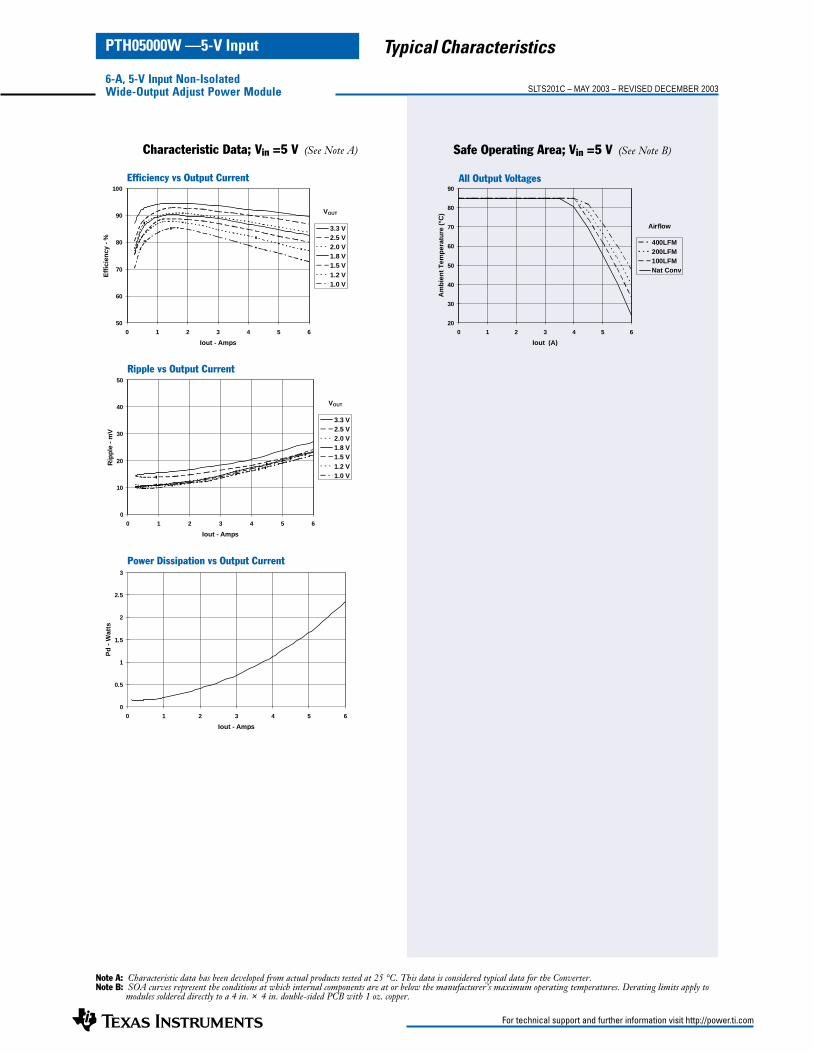
Note A: Characteristic data has been developed from actual products tested at 25 °C. This data is considered typical data for the Converter.Note B: SOA curves represent the conditions at which internal components are at or below the manufacturer’s maximum operating temperatures. Derating limits apply to
modules soldered directly to a 4 in. × 4 in. double-sided PCB with 1 oz. copper.
Typical Characteristics
Characteristic Data; Vin =5 V (See Note A)
Efficiency vs Output Current
Power Dissipation vs Output Current
Ripple vs Output Current
20
30
40
50
60
70
80
90
0 1 2 3 4 5 6
Iout (A)
Am
bie
nt
Tem
per
atu
re (
°C)
400LFM200LFM100LFMNat Conv
Airflow
Safe Operating Area; Vin =5 V (See Note B)
All Output Voltages
50
60
70
80
90
100
0 1 2 3 4 5 6
Iout - Amps
Eff
icie
ncy
- %
3.3 V2.5 V2.0 V1.8 V1.5 V1.2 V1.0 V
VOUT
0
10
20
30
40
50
0 1 2 3 4 5 6
Iout - Amps
Rip
ple
- m
V
3.3 V2.5 V2.0 V1.8 V1.5 V1.2 V1.0 V
VOUT
0
0.5
1
1.5
2
2.5
3
0 1 2 3 4 5 6
Iout - Amps
Pd
- W
atts
6-A, 5-V Input Non-IsolatedWide-Output Adjust Power Module SLTS201C – MAY 2003 – REVISED DECEMBER 2003
PTH05000W —5-V Input

Application Notes
For technical support and further information visit http://power.ti.com
PTH05000W
Capacitor Recommendations for the PTH05000WWide-Output Adjust Power Modules
Input CapacitorThe recommended input capacitor(s) is determined bythe 330 µF minimum capacitance and 300 mArms mini-mum ripple current rating.
Ripple current, less than 300 mΩ equivalent series resis-tance (ESR), and temperature are the major considerationswhen selecting input capacitors. Unlike polymer tantalum,regular tantalum capacitors have a recommended mini-mum voltage rating of 2 × (maximum DC voltage + ACripple). This is standard practice to ensure reliability.
For improved ripple reduction on the input bus, ceramiccapacitors [2] may used to complement electrolytic types,and achieve the minimum required capacitance.
Output Capacitors (Optional)For applications with load transients (sudden changes inload current), regulator response will benefit from anexternal output capacitance. The recommended outputcapacitance of 100 µF will allow the module to meetits transient response specification (see product data sheet).For most applications, a high quality computer-gradealuminum electrolytic capacitor is adequate. These capaci-tors provide decoupling over the frequency range, 2 kHzto 150 kHz, and are suitable for ambient temperaturesabove 0 °C. For operation below 0 °C tantalum, ceramicor Os-Con type capacitors are recommended. When usingone or more non-ceramic capacitors, the calculated equiva-lent ESR should be no lower than 4 mΩ (7 mΩ using themanufacturer’s maximum ESR for a single capacitor). Alist of preferred low-ESR type capacitors are identifiedin Table 1-1.
Ceramic CapacitorsAbove 150 kHz the performance of aluminum electrolyticcapacitors becomes less effective. To further improve thereflected input ripple current [2] or the output transientresponse, multilayer ceramic capacitors can also be added.Ceramic capacitors have very low ESR and their resonantfrequency is higher than the bandwidth of the regulator.When used on the output their combined ESR is notcritical as long as the total value of ceramic capacitancedoes not exceed 300 µF. Also, to prevent the formation oflocal resonances, do not place more than five identical ce-ramic capacitors in parallel with values of 10 µF or greater.
Tantalum CapacitorsTantalum type capacitors can be used at both the inputand output, and are recommended for applications wherethe ambient operating temperature can be less than 0 °C.The AVX TPS, Sprague 593D/594/595 and Kemet T495/
T510 capacitor series are suggested over many othertantalum types due to their higher rated surge, powerdissipation, and ripple current capability. As a cautionmany general purpose tantalum capacitors have consid-erably higher ESR, reduced power dissipation and lowerripple current capability. These capacitors are also lessreliable as they have lower power dissipation and surgecurrent ratings. Tantalum capacitors that do not have astated ESR or surge current rating are not recommendedfor power applications.
When specifying Os-Con and polymer tantalum capacitorsfor the output, the minimum ESR limit will be encoun-tered well before the maximum capacitance value isreached.
Capacitor TableTable 1-1 identifies the characteristics of capacitors from anumber of vendors with acceptable ESR and ripple current(rms) ratings. The recommended number of capacitorsrequired at both the input and output buses is identifiedfor each capacitor type.
This is not an extensive capacitor list. Capacitors from othervendors are available with comparable specifications. Thoselisted are for guidance. The RMS ripple current rating andESR (at 100 kHz) are critical parameters necessary to insureboth optimum regulator performance and long capacitor life.
Designing for Very Fast Load TransientsThe transient response of the DC/DC converter has beencharacterized using a load transient with a di/dt of 1 A/µs.The typical voltage deviation for this load transient isgiven in the data sheet specification table using theoptional value of output capacitance. As the di/dt of atransient is increased, the response of a converter’s regu-lation circuit ultimately depends on its output capacitordecoupling network. This is an inherent limitation withany DC/DC converter once the speed of the transientexceeds its bandwidth capability. If the target applicationspecifies a higher di/dt or lower voltage deviation, therequirement can only be met with additional outputcapacitor decoupling. In these cases special attentionmust be paid to the type, value and ESR of the capacitorsselected.
If the transient performance requirements exceed thatspecified in the data sheet, the selection of output ca-pacitors becomes more important. For further guidanceconsult the separate application note, “Selecting OutputCapacitors for PTH Products in High-Performance Applica-tions.”

Application Notes continued
For technical support and further information visit http://power.ti.com
PTH05000 Series
Table 1-1: Input/Output Capacitors
[1] A total capacitance of 300 µF is acceptable based on the surge current capability of ceramic capacitors.[2] A ceramic capacitor may be used to complement electrolytic types at the input to further reduce high-frequency ripple current.
/epyT,rodneVroticapaC)elytS(seireS scitsiretcarahCroticapaC ytitnauQ
gnikroWegatloV )Fµ(eulaV
RSE.xaMzHk001ta
elppiR.xaMC°58tatnerruC
)smrI(
eziSlacisyhP)mm(
tupnIsuB
tuptuOsuB rebmuNrodneV
cinosanaP)DMS(munimulA-yloP,AW
)DMS(munimulA,CF)DMS(munimulA,KF)laidaR(munimulA,CF
V01V61V61V01
Fµ033Fµ033Fµ033Fµ033
.0 530 Ω051.0 Ω061.0 Ω711.0 Ω
Am0082Am076Am006Am055
8× 9.601 × 2.01
8× 2.018× 5.11
1111
≤3≤3≤3≤3
P121A1AWFEEP133C1CFVEEP133C1KFVEE
133A1CFUEE
noC–imehCdetinU)DMS(mulA-yloP,AXP
)laidaR(noc-sO,SF)laidaR(munimulA,ZXL)DMS(numimulA,ZVM
)laidaR(munimulA-yloP,ASP
V01V01V61V52V3.6
033 FµFµ033Fµ033
033 FµFµ093
420.0 Ω520.0 Ω021.0 Ω071.0 Ω800.0 Ω
Am0773Am0053Am555Am054Am0805
01 × 7.701 × 5.018× 218× 01
8× 5.11
11111
≤3≤3≤3≤3≤1
PT08JM133CV01AXPM033SF01
LL21x8M133BV61ZXLPT01HM133CV52ZVM
11HM093BV3.6ASP
munimulAnocihciN)DMS(GW
)laidaR(MPV61V01
033 Fµ033 Fµ
051.0 Ω061.0 Ω
Am076Am064
01 × 018× 5.11
11
≤3≤3
SG1RNM133C1GWUHHM133A1MPU
oynaS)DMS(noc-sO,PVS
)laidaR(noc-sO,PS)DMS(remyloPpacsoP,EPT
V01V01V3.6
033 FµFµ074Fµ033
520.0 Ω510.0 Ω520.0 Ω
Am0073Am0054Am0042
01 ×801 × 5.01L3.7 × W3.4
111
≤3≤2≤3
XM033PVS01M074PS01
LM033EPT6
SPTmulatnaTXVA)DMS(
V01V01
Fµ033Fµ033
01.0 0 Ω060.0 Ω
Am0011Am0002
L3.7× W3.4 × H1.4
11
≤3≤3
0010R010M733VSPT0600R010M733VSPT
)DMS(temeK,025T munimulAyloP
.mulA-yloPcinagrO,035T
V01V01
Fµ033Fµ033
040.0 Ω510.0 Ω
Am0021Am0011
L3.7 × W7.5× H0.4
11
≤3≤2
SA010M733X025TSA010M733X035T
eugarpS-yahsiV)DMS(mulatnaT,D495)DMS(mulatnaT,D595
)DMS(noc-sO,PVS49)laidaR(noc-sO,AS49
V01V01V3.6V3,6
Fµ033Fµ033Fµ033Fµ033
540.0 Ω041.0 Ω520.0 Ω520.0 Ω
Am0041Am0001Am0033Am0053
L3.7× W0.6 × H1.4
01 ×801 × 5.01
1111
≤3≤3≤3≤3
T2R0100X733D495T2D0100X733D5958F3R60X733PVS49PBF3R60X733AS49
)DMS(R5XcimareC,temeK V61V3.6
0174
200.0 Ω200.0 Ω
— esac0121mm5223
1 ]2[1 ]2[
≤3≤2
CAP4M601C0121CCAP9K674C0121C
cimareC,ataruM R5X )DMS( V3.6V3.6V61V61
001742201
200.0 Ω — esac0121mm5223
3 ]1[1 ]2[1 ]2[1 ]2[
1≤≤2≤3≤3
M701J06RE23MRGM674J06RE23MRGK622C16RE23MRGK601C16RD23MRG
cimareC,KDT R5X )DMS( V3.6V3.6V61V61
001742201
200.0 Ω — esac0121mm5223
3 ]1[1 ]2[1 ]2[1 ]2[
1≤≤2≤3≤3
TM701J0R5X5223CTM674J0R5X5223CTM622C1R5X5223CTM601C1R5X5223C

Application Notes
For technical support and further information visit http://power.ti.com
Adjusting the Output Voltage of the PTH05000WWide-Output Adjust Power Modules
The Vo Adjust control (pin 4) sets the output voltage ofthe PTH05000Wproduct. The adjustment range isfrom 0.9 V to 3.6 V. The adjustment method requiresthe addition of a single external resistor, Rset, that mustbe connected directly between the Vo Adjust and GNDpins 1. Table 2-1 gives the preferred value of the externalresistor for a number of standard voltages, along with theactual output voltage that this resistance value provides.
For other output voltages the value of the required resistorcan either be calculated using the following formula, orsimply selected from the range of values given in Table 2-2.Figure 2-1 shows the placement of the required resistor.
Rset = 10 kΩ · 0.891 V – 3.24 kΩVout – 0.9 V
Figure 2-1; Vo Adjust Resistor Placement
Notes:1. Use a 0.1 W resistor. The tolerance should be 1 %,
with a temperature stability of 100 ppm/°C (or better).Place the resistor as close to the regulator as possible.Connect the resistor directly between pins 4 and 1using dedicated PCB traces.
2. Never connect capacitors from Vo Adjust to either GND orVout. Any capacitance added to the Vo Adjust pin will affectthe stability of the regulator.
0.900 Open0.925 353 kΩ0.950 175 kΩ0.975 116 kΩ1.000 85.9 kΩ1.025 68.0 kΩ1.050 56.2 kΩ1.075 47.7 kΩ1.100 41.3 kΩ1.125 36.4 kΩ1.150 32.4 kΩ1.175 29.2 kΩ1.200 26.5 kΩ1.225 24.2 kΩ1.250 22.2 kΩ1.275 20.5 kΩ1.300 19.0 kΩ1.325 17.7 kΩ1.350 16.6 kΩ1.375 15.5 kΩ1.400 14.6 kΩ1.425 13.7 kΩ1.450 13.0 kΩ1.475 12.3 kΩ1.50 11.6 kΩ1.55 10.5 kΩ1.60 9.49 kΩ1.65 8.64 kΩ1.70 7.90 kΩ1.75 7.24 kΩ1.80 6.66 kΩ1.85 6.14 kΩ1.90 5.67 kΩ1.95 5.25 kΩ
Vout (Standard) Rset (Pref’d Value) Vout (Actual)
3.3 V 475 Ω 3.298V2.5 V 2.32 kΩ 2.502 V2 V 4.87 kΩ 1.999 V1.8 V 6.65 kΩ 1.801 V1.5 V 11.5 kΩ 1.504 V1.2 V 26.1 kΩ 1.204 V1 V 84.5 kΩ 1.001 V0.9 V Open 0.9 V
Table 2-1; Preferred Values of Rset for Standard Output Voltages
Table 2-2; Output Voltage Set-Point Resistor ValuesVa Req’d Rset Va Req’d Rset
2.00 4.86 kΩ2.05 4.51 kΩ2.10 4.19 kΩ2.15 3.89 kΩ2.20 3.61 kΩ2.25 3.36 kΩ2.30 3.12 kΩ2.35 2.90 kΩ2.40 2.70 kΩ2.45 2.51 kΩ2.50 2.33 kΩ2.55 2.16 kΩ2.60 2.00 kΩ2.65 1.85 kΩ2.70 1.71 kΩ2.75 1.58 kΩ2.80 1.45 kΩ2.85 1.33 kΩ2.90 1.22 kΩ2.95 1.11 kΩ3.00 1.00 kΩ3.05 904 Ω3.10 810 Ω3.15 720 Ω3.20 634 Ω3.25 551 Ω3.30 473 Ω3.35 397 Ω3.40 324 Ω3.45 254 Ω3.50 187 Ω3.55 122 Ω3.60 60 Ω
PTH05000WVIN
1
4
52
3CIN
330µF(Required)
+ COUT
100µF(Optional)
+
Inhibit
GND GND
VOUT
RSET
0.1 W, 1 %
VO Adj
GNDInhibit
VINVO
PTH05000W
Application Notes
For technical support and further information visit http://power.ti.com
Output On/Off InhibitFor applications requiring output voltage on/off control,the PTH03000W & PTH05000W power modules in-corporate an output on/off Inhibit control (pin 3). Theinhibit feature can be used wherever there is a require-ment for the output voltage from the regulator to beturned off.
The power module functions normally when the Inhibitpin is left open-circuit, providing a regulated outputwhenever a valid source voltage is connected to Vin withrespect to GND.
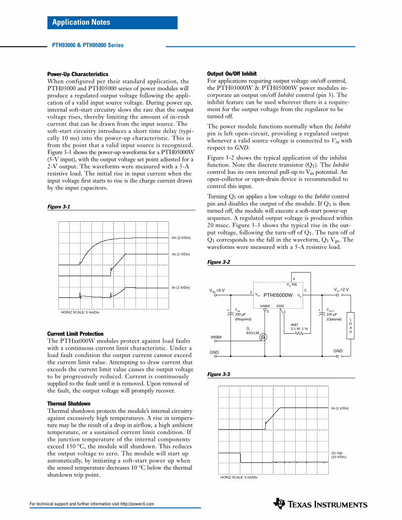
Figure 3-2 shows the typical application of the inhibitfunction. Note the discrete transistor (Q1). The Inhibitcontrol has its own internal pull-up to Vin potential. Anopen-collector or open-drain device is recommended tocontrol this input.
Turning Q1 on applies a low voltage to the Inhibit controlpin and disables the output of the module. If Q1 is thenturned off, the module will execute a soft-start power-upsequence. A regulated output voltage is produced within20 msec. Figure 3-3 shows the typical rise in the out-put voltage, following the turn-off of Q1. The turn off ofQ1 corresponds to the fall in the waveform, Q1 Vgs. Thewaveforms were measured with a 5-A resistive load.
Figure 3-2
Figure 3-3
Power-Up CharacteristicsWhen configured per their standard application, thePTH03000 and PTH05000 series of power modules willproduce a regulated output voltage following the appli-cation of a valid input source voltage. During power up,internal soft-start circuitry slows the rate that the outputvoltage rises, thereby limiting the amount of in-rushcurrent that can be drawn from the input source. Thesoft-start circuitry introduces a short time delay (typi-cally 10 ms) into the power-up characteristic. This isfrom the point that a valid input source is recognized.Figure 3-1 shows the power-up waveforms for a PTH05000W(5-V input), with the output voltage set point adjusted for a2-V output. The waveforms were measured with a 5-Aresistive load. The initial rise in input current when theinput voltage first starts to rise is the charge current drawnby the input capacitors.
Figure 3-1
Current Limit ProtectionThe PTHxx000W modules protect against load faultswith a continuous current limit characteristic. Under aload fault condition the output current cannot exceedthe current limit value. Attempting to draw current thatexceeds the current limit value causes the output voltageto be progressively reduced. Current is continuouslysupplied to the fault until it is removed. Upon removal ofthe fault, the output voltage will promptly recover.
Thermal ShutdownThermal shutdown protects the module’s internal circuitryagainst excessively high temperatures. A rise in tempera-ture may be the result of a drop in airflow, a high ambienttemperature, or a sustained current limit condition. Ifthe junction temperature of the internal componentsexceed 150 °C, the module will shutdown. This reducesthe output voltage to zero. The module will start upautomatically, by initiating a soft-start power up whenthe sensed temperature decreases 10 °C below the thermalshutdown trip point.
PTH03000 & PTH05000 Series
PTH05000WVIN =5 V
1
4
52
3CIN
330 µF(Required)
+ COUT
100 µF(Optional)
+
Inhibit
GND
VO =2 V
4k870.1 W, 1 %
VO Adj
GNDInhibit
VIN VO
LOAD
GND
Q1
BSS138
Vo (1 V/Div)
Q1 Vgs(10 V/Div)
HORIZ SCALE: 5 ms/Div
Vin (2 V/Div)
Vo (1 V/Div)
Iin (2 A/Div)
HORIZ SCALE: 5 ms/Div
Application Notes
For technical support and further information visit http://power.ti.com
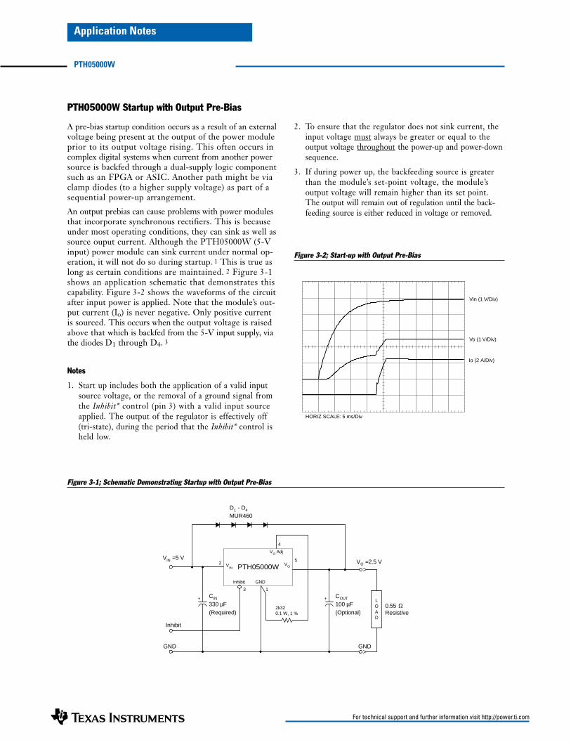
PTH05000W Startup with Output Pre-Bias
A pre-bias startup condition occurs as a result of an externalvoltage being present at the output of the power moduleprior to its output voltage rising. This often occurs incomplex digital systems when current from another powersource is backfed through a dual-supply logic componentsuch as an FPGA or ASIC. Another path might be viaclamp diodes (to a higher supply voltage) as part of asequential power-up arrangement.
An output prebias can cause problems with power modulesthat incorporate synchronous rectifiers. This is becauseunder most operating conditions, they can sink as well assource ouput current. Although the PTH05000W (5-Vinput) power module can sink current under normal op-eration, it will not do so during startup. 1 This is true aslong as certain conditions are maintained. 2 Figure 3-1shows an application schematic that demonstrates thiscapability. Figure 3-2 shows the waveforms of the circuitafter input power is applied. Note that the module’s out-put current (Io) is never negative. Only positive currentis sourced. This occurs when the output voltage is raisedabove that which is backfed from the 5-V input supply, viathe diodes D1 through D4. 3
Notes
1. Start up includes both the application of a valid inputsource voltage, or the removal of a ground signal fromthe Inhibit* control (pin 3) with a valid input sourceapplied. The output of the regulator is effectively off(tri-state), during the period that the Inhibit* control isheld low.
Figure 3-2; Start-up with Output Pre-Bias
Figure 3-1; Schematic Demonstrating Startup with Output Pre-Bias
2. To ensure that the regulator does not sink current, theinput voltage must always be greater or equal to theoutput voltage throughout the power-up and power-downsequence.
3. If during power up, the backfeeding source is greaterthan the module’s set-point voltage, the module’soutput voltage will remain higher than its set point.The output will remain out of regulation until the back-feeding source is either reduced in voltage or removed.
PTH05000W
Vin (1 V/Div)
Vo (1 V/Div)
Io (2 A/Div)
HORIZ SCALE: 5 ms/Div
PTH05000WVIN =5 V
1
4
52
3
CIN
330 µF(Required)
+ COUT
100 µF(Optional)
+
Inhibit
GND
VO =2.5 V
2k320.1 W, 1 %
VO Adj
GNDInhibit
VIN
VO
LOAD
GND
D1 - D4
MUR460
0.55 ΩResistive

PACKAGE OPTION ADDENDUM
www.ti.com 27-Apr-2017
Addendum-Page 1
PACKAGING INFORMATION
Orderable Device Status(1)
Package Type PackageDrawing
Pins PackageQty
Eco Plan(2)
Lead/Ball Finish(6)
MSL Peak Temp(3)
Op Temp (°C) Device Marking(4/5)
Samples
PTH05000WAD ACTIVE Through-Hole Module
EUS 5 56 RoHS (InWork) & Green
(In Work)
SN N / A for Pkg Type -40 to 85
PTH05000WAH ACTIVE Through-Hole Module
EUS 5 56 RoHS (InWork) & Green
(In Work)
SN N / A for Pkg Type -40 to 85
PTH05000WAS ACTIVE SurfaceMount Module
EUT 5 49 RoHS (InWork) & Green
(In Work)
SNPB Level-1-235C-UNLIM/Level-3-260C-168HRS
-40 to 85
PTH05000WAST ACTIVE SurfaceMount Module
EUT 5 250 RoHS (InWork) & Green
(In Work)
SNPB Level-1-235C-UNLIM/Level-3-260C-168HRS
-40 to 85
PTH05000WAZ ACTIVE SurfaceMount Module
EUT 5 49 RoHS (InWork) & Green
(In Work)
SNAGCU Level-3-260C-168 HR -40 to 85
PTH05000WAZT ACTIVE SurfaceMount Module
EUT 5 250 RoHS (InWork) & Green
(In Work)
SNAGCU Level-3-260C-168 HR -40 to 85
(1) The marketing status values are defined as follows:ACTIVE: Product device recommended for new designs.LIFEBUY: TI has announced that the device will be discontinued, and a lifetime-buy period is in effect.NRND: Not recommended for new designs. Device is in production to support existing customers, but TI does not recommend using this part in a new design.PREVIEW: Device has been announced but is not in production. Samples may or may not be available.OBSOLETE: TI has discontinued the production of the device.
(2) RoHS: TI defines "RoHS" to mean semiconductor products that are compliant with the current EU RoHS requirements for all 10 RoHS substances, including the requirement that RoHS substancedo not exceed 0.1% by weight in homogeneous materials. Where designed to be soldered at high temperatures, "RoHS" products are suitable for use in specified lead-free processes. TI mayreference these types of products as "Pb-Free".RoHS Exempt: TI defines "RoHS Exempt" to mean products that contain lead but are compliant with EU RoHS pursuant to a specific EU RoHS exemption.Green: TI defines "Green" to mean the content of Chlorine (Cl) and Bromine (Br) based flame retardants meet JS709B low halogen requirements of <=1000ppm threshold. Antimony trioxide basedflame retardants must also meet the <=1000ppm threshold requirement.
(3) MSL, Peak Temp. - The Moisture Sensitivity Level rating according to the JEDEC industry standard classifications, and peak solder temperature.
(4) There may be additional marking, which relates to the logo, the lot trace code information, or the environmental category on the device.
PACKAGE OPTION ADDENDUM
www.ti.com 27-Apr-2017
Addendum-Page 2
(5) Multiple Device Markings will be inside parentheses. Only one Device Marking contained in parentheses and separated by a "~" will appear on a device. If a line is indented then it is a continuationof the previous line and the two combined represent the entire Device Marking for that device.
(6) Lead/Ball Finish - Orderable Devices may have multiple material finish options. Finish options are separated by a vertical ruled line. Lead/Ball Finish values may wrap to two lines if the finishvalue exceeds the maximum column width.
Important Information and Disclaimer:The information provided on this page represents TI's knowledge and belief as of the date that it is provided. TI bases its knowledge and belief on informationprovided by third parties, and makes no representation or warranty as to the accuracy of such information. Efforts are underway to better integrate information from third parties. TI has taken andcontinues to take reasonable steps to provide representative and accurate information but may not have conducted destructive testing or chemical analysis on incoming materials and chemicals.TI and TI suppliers consider certain information to be proprietary, and thus CAS numbers and other limited information may not be available for release.
In no event shall TI's liability arising out of such information exceed the total purchase price of the TI part(s) at issue in this document sold by TI to Customer on an annual basis.


IMPORTANT NOTICE
Texas Instruments Incorporated (TI) reserves the right to make corrections, enhancements, improvements and other changes to itssemiconductor products and services per JESD46, latest issue, and to discontinue any product or service per JESD48, latest issue. Buyersshould obtain the latest relevant information before placing orders and should verify that such information is current and complete.TI’s published terms of sale for semiconductor products (http://www.ti.com/sc/docs/stdterms.htm) apply to the sale of packaged integratedcircuit products that TI has qualified and released to market. Additional terms may apply to the use or sale of other types of TI products andservices.Reproduction of significant portions of TI information in TI data sheets is permissible only if reproduction is without alteration and isaccompanied by all associated warranties, conditions, limitations, and notices. TI is not responsible or liable for such reproduceddocumentation. Information of third parties may be subject to additional restrictions. Resale of TI products or services with statementsdifferent from or beyond the parameters stated by TI for that product or service voids all express and any implied warranties for theassociated TI product or service and is an unfair and deceptive business practice. TI is not responsible or liable for any such statements.Buyers and others who are developing systems that incorporate TI products (collectively, “Designers”) understand and agree that Designersremain responsible for using their independent analysis, evaluation and judgment in designing their applications and that Designers havefull and exclusive responsibility to assure the safety of Designers' applications and compliance of their applications (and of all TI productsused in or for Designers’ applications) with all applicable regulations, laws and other applicable requirements. Designer represents that, withrespect to their applications, Designer has all the necessary expertise to create and implement safeguards that (1) anticipate dangerousconsequences of failures, (2) monitor failures and their consequences, and (3) lessen the likelihood of failures that might cause harm andtake appropriate actions. Designer agrees that prior to using or distributing any applications that include TI products, Designer willthoroughly test such applications and the functionality of such TI products as used in such applications.TI’s provision of technical, application or other design advice, quality characterization, reliability data or other services or information,including, but not limited to, reference designs and materials relating to evaluation modules, (collectively, “TI Resources”) are intended toassist designers who are developing applications that incorporate TI products; by downloading, accessing or using TI Resources in anyway, Designer (individually or, if Designer is acting on behalf of a company, Designer’s company) agrees to use any particular TI Resourcesolely for this purpose and subject to the terms of this Notice.TI’s provision of TI Resources does not expand or otherwise alter TI’s applicable published warranties or warranty disclaimers for TIproducts, and no additional obligations or liabilities arise from TI providing such TI Resources. TI reserves the right to make corrections,enhancements, improvements and other changes to its TI Resources. TI has not conducted any testing other than that specificallydescribed in the published documentation for a particular TI Resource.Designer is authorized to use, copy and modify any individual TI Resource only in connection with the development of applications thatinclude the TI product(s) identified in such TI Resource. NO OTHER LICENSE, EXPRESS OR IMPLIED, BY ESTOPPEL OR OTHERWISETO ANY OTHER TI INTELLECTUAL PROPERTY RIGHT, AND NO LICENSE TO ANY TECHNOLOGY OR INTELLECTUAL PROPERTYRIGHT OF TI OR ANY THIRD PARTY IS GRANTED HEREIN, including but not limited to any patent right, copyright, mask work right, orother intellectual property right relating to any combination, machine, or process in which TI products or services are used. Informationregarding or referencing third-party products or services does not constitute a license to use such products or services, or a warranty orendorsement thereof. Use of TI Resources may require a license from a third party under the patents or other intellectual property of thethird party, or a license from TI under the patents or other intellectual property of TI.TI RESOURCES ARE PROVIDED “AS IS” AND WITH ALL FAULTS. TI DISCLAIMS ALL OTHER WARRANTIES ORREPRESENTATIONS, EXPRESS OR IMPLIED, REGARDING RESOURCES OR USE THEREOF, INCLUDING BUT NOT LIMITED TOACCURACY OR COMPLETENESS, TITLE, ANY EPIDEMIC FAILURE WARRANTY AND ANY IMPLIED WARRANTIES OFMERCHANTABILITY, FITNESS FOR A PARTICULAR PURPOSE, AND NON-INFRINGEMENT OF ANY THIRD PARTY INTELLECTUALPROPERTY RIGHTS. TI SHALL NOT BE LIABLE FOR AND SHALL NOT DEFEND OR INDEMNIFY DESIGNER AGAINST ANY CLAIM,INCLUDING BUT NOT LIMITED TO ANY INFRINGEMENT CLAIM THAT RELATES TO OR IS BASED ON ANY COMBINATION OFPRODUCTS EVEN IF DESCRIBED IN TI RESOURCES OR OTHERWISE. IN NO EVENT SHALL TI BE LIABLE FOR ANY ACTUAL,DIRECT, SPECIAL, COLLATERAL, INDIRECT, PUNITIVE, INCIDENTAL, CONSEQUENTIAL OR EXEMPLARY DAMAGES INCONNECTION WITH OR ARISING OUT OF TI RESOURCES OR USE THEREOF, AND REGARDLESS OF WHETHER TI HAS BEENADVISED OF THE POSSIBILITY OF SUCH DAMAGES.Unless TI has explicitly designated an individual product as meeting the requirements of a particular industry standard (e.g., ISO/TS 16949and ISO 26262), TI is not responsible for any failure to meet such industry standard requirements.Where TI specifically promotes products as facilitating functional safety or as compliant with industry functional safety standards, suchproducts are intended to help enable customers to design and create their own applications that meet applicable functional safety standardsand requirements. Using products in an application does not by itself establish any safety features in the application. Designers mustensure compliance with safety-related requirements and standards applicable to their applications. Designer may not use any TI products inlife-critical medical equipment unless authorized officers of the parties have executed a special contract specifically governing such use.Life-critical medical equipment is medical equipment where failure of such equipment would cause serious bodily injury or death (e.g., lifesupport, pacemakers, defibrillators, heart pumps, neurostimulators, and implantables). Such equipment includes, without limitation, allmedical devices identified by the U.S. Food and Drug Administration as Class III devices and equivalent classifications outside the U.S.TI may expressly designate certain products as completing a particular qualification (e.g., Q100, Military Grade, or Enhanced Product).Designers agree that it has the necessary expertise to select the product with the appropriate qualification designation for their applicationsand that proper product selection is at Designers’ own risk. Designers are solely responsible for compliance with all legal and regulatoryrequirements in connection with such selection.Designer will fully indemnify TI and its representatives against any damages, costs, losses, and/or liabilities arising out of Designer’s non-compliance with the terms and provisions of this Notice.
Mailing Address: Texas Instruments, Post Office Box 655303, Dallas, Texas 75265Copyright © 2017, Texas Instruments Incorporated