pulse and digital circuits laboratory …lendi.org/ece/labmanuals/pdc_lab-min.pdf · 13. bootstrap...
TRANSCRIPT

PDC LAB
Dept of ECE, Lendi Institute of Engineering and Technology Page 1
LENDI INSTITUTE OF ENGINEERING AND TECHNOLOGY (Approved by A.I.C.T.E & Affiliated to JNTU, Kakinada)
Jonnada (Village), Denkada (Mandal), Vizianagaram Dist – 535005
Phone No. 08922-241111, 241112 E-Mail: [email protected] Website: www.lendi.org
DEPARTMENT OF ELECTRONICS AND COMMUNICATION ENGINEERING
PULSE AND DIGITAL CIRCUITS LABORATORY
OBSERVATION
Name:
Regd No: Year&Sem:
Academic Year:
PDC LAB
Dept of ECE, Lendi Institute of Engineering and Technology Page 2
LIST OF EXPERIMENTS
Minimum Twelve experiments to be conducted:
1. Linear wave shaping.
2. Non Linear wave shaping – Clippers.
3. Non Linear wave shaping – Clampers.
4. Transistor as a switch.
5. Study of Logic Gates & Some applications.
6. Study of Flip-Flops & some applications.
7. Sampling Gates.
8. Astable Multivibrator.
9. Monostable Multivibrator.
10. Bistable Multivibrator.
11. Schmitt Trigger.
12. UJT Relaxation Oscillator.
13. Bootstrap sweep circuit.
PDC LAB
Dept of ECE, Lendi Institute of Engineering and Technology Page 3
INTRODUCTION TO PDC LAB:
This Lab is organized into 12 experiments and the outline is as follows:
When non-sinusoidal signals are transmitted through a linear network, the shape of the waveform
undergoes a change. This process is called linear wave shaping and is our 1st experiment.
In communication systems it is required to remove a part of the waveform above or below
some reference level, this process is called clipping. In many pulse systems, quite often a dc level is
required to be added to a waveform to fix the top or bottom of waveform at some reference level,
this process is called clamping. Clipping and Clamping together is called non- Linear wave shaping
and is our 2nd
and 3rd
experiments.
The switching characteristics of transistors are designed in the 4th
experiment.
Logic gates are the fundamental building blocks of any digital system. Realization of logic
gates using diodes and transistors are done in the 5th
experiment.
The different types of flip- flops are designed in the 8th
experiments which are used for
storing digital data.
When signals are to be transmitted only for specified intervals of time and are to be
blocked during other intervals of time, we require sampling gates. Various types of sampling gates
are designed in our 7th
experiment.
Memory is the basic requirement of all computers. The basic memory element is flip- flop
i.e. the bistable multivibrator. The monostable multivibrator is the basic gating circuit. The astable
multivibrator is used as a master oscillator and the Schmitt trigger circuit as a basic voltage
comparator. The various types of multivibrators designing is done in the 8,9,10 and 11 experiments.
Time- base generators are essential for display of signals on the screen. Voltage and current
time- base generators are designed in 12th
and 13th
experiments.
PDC LAB
Dept of ECE, Lendi Institute of Engineering and Technology Page 4
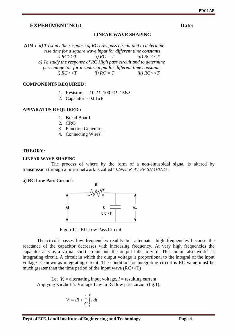
EXPERIMENT NO:1 Date:
LINEAR WAVE SHAPING
AIM : a) To study the response of RC Low pass circuit and to determine
rise time for a square wave input for different time constants.
i) RC>>T ii) RC = T iii) RC<<T
b) To study the response of RC High pass circuit and to determine
percentage tilt for a square input for different time constants.
i) RC>>T ii) RC = T iii) RC<<T
COMPONENTS REQUIRED :
1. Resistors - 10k, 100 k, 1M
2. Capacitor - 0.01F
APPARATUS REQUIRED :
1. Bread Board.
2. CRO
3. Function Generator.
4. Connecting Wires.
THEORY:
LINEAR WAVE SHAPING
The process of where by the form of a non-sinusoidal signal is altered by
transmission through a linear network is called “LINEAR WAVE SHAPING”.
a) RC Low Pass Circuit :
Figure1.1: RC Low Pass Circuit.
The circuit passes low frequencies readily but attenuates high frequencies because the
reactance of the capacitor decreases with increasing frequency. At very high frequencies the
capacitor acts as a virtual short circuit and the output falls to zero. This circuit also works as
integrating circuit. A circuit in which the output voltage is proportional to the integral of the input
voltage is known as integrating circuit. The condition for integrating circuit is RC value must be
much greater than the time period of the input wave (RC>>T)
Let Vi = alternating input voltage, i = resulting current
Applying Kirchoff‟s Voltage Law to RC low pass circuit (fig.1).
T
o
i dtiC
iRV .1
PDC LAB
Dept of ECE, Lendi Institute of Engineering and Technology Page 5
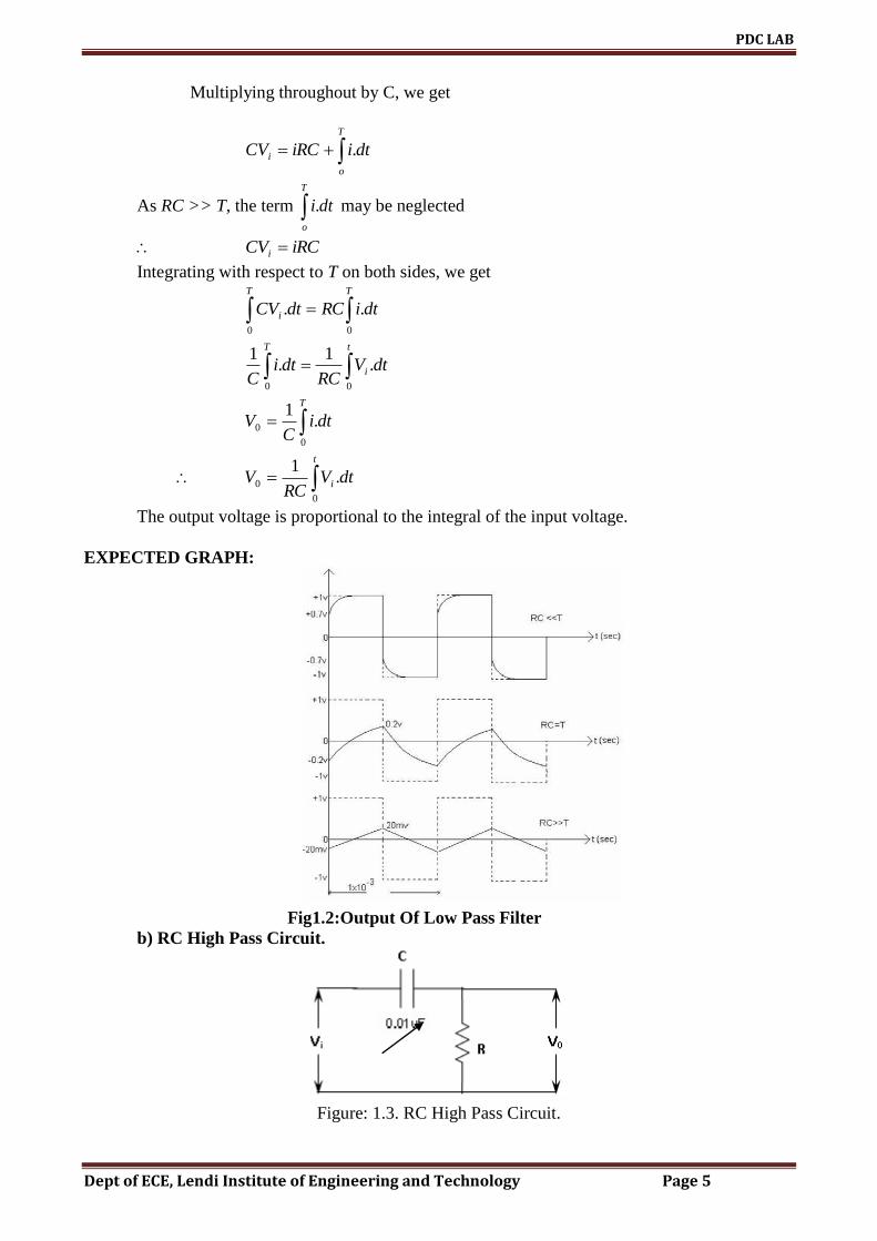
Multiplying throughout by C, we get
T
o
i dtiiRCCV .
As RC >> T, the term T
o
dti. may be neglected
iRCCVi
Integrating with respect to T on both sides, we get
T T
i dtiRCdtCV0 0
..
T t
i dtVRC
dtiC
0 0
.1
.1
T
dtiC
V0
0 .1
t
i dtVRC
V0
0 .1
The output voltage is proportional to the integral of the input voltage.
EXPECTED GRAPH:
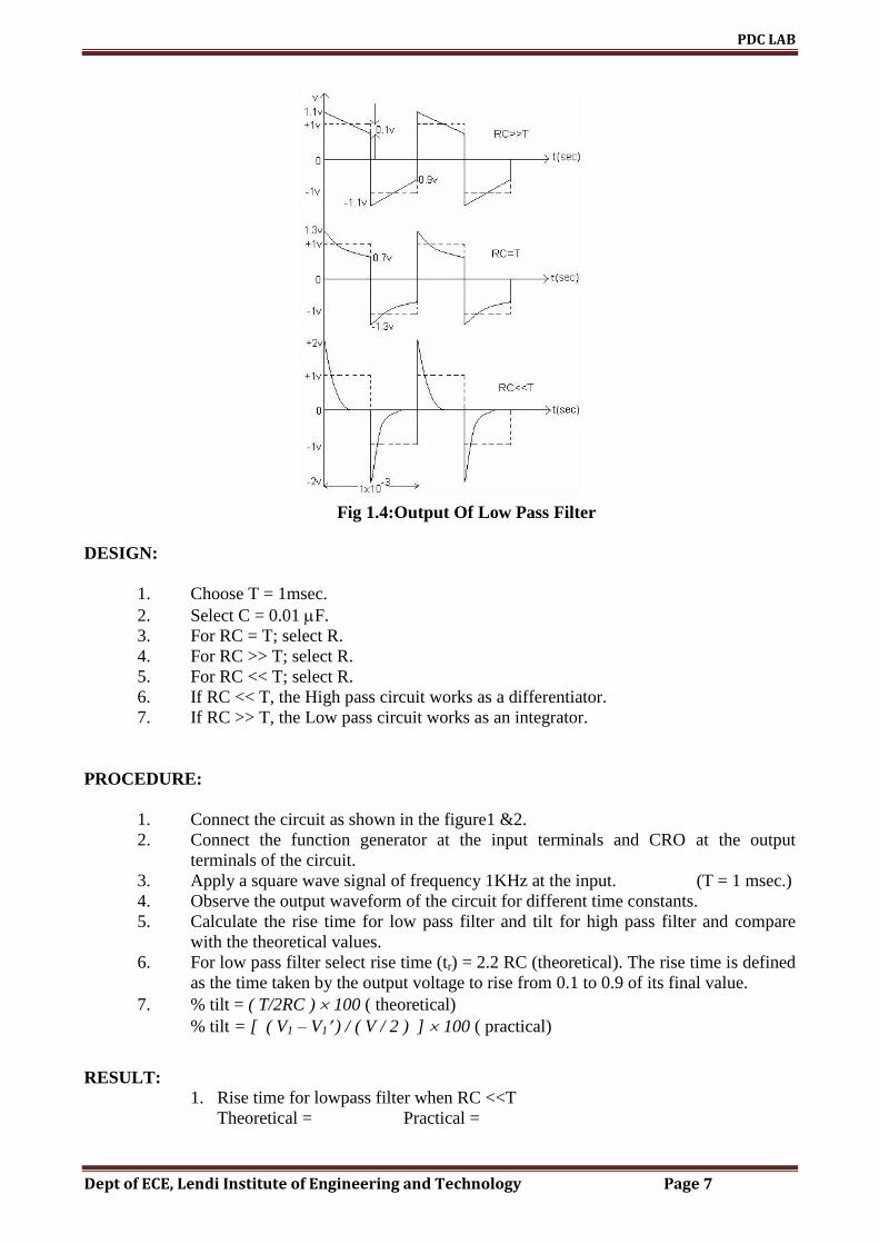
Fig1.2:Output Of Low Pass Filter
b) RC High Pass Circuit.
Figure: 1.3. RC High Pass Circuit.
PDC LAB
Dept of ECE, Lendi Institute of Engineering and Technology Page 6
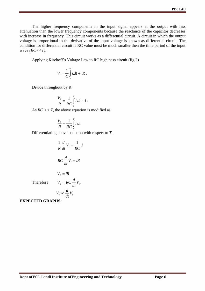
The higher frequency components in the input signal appears at the output with less
attenuation than the lower frequency components because the reactance of the capacitor decreases
with increase in frequency. This circuit works as a differential circuit. A circuit in which the output
voltage is proportional to the derivative of the input voltage is known as differential circuit. The
condition for differential circuit is RC value must be much smaller then the time period of the input
wave (RC<<T).
Applying Kirchoff‟s Voltage Law to RC high pass circuit (fig.2)
T
o
i iRdtiC
V .1
.
Divide throughout by R
T
o
i idtiRCR
V.
1.
As RC << T, the above equation is modified as
T
o
i dtiRCR
V.
1
Differentiating above equation with respect to T.
iRC
Vdt
d
Ri .
11
iRVdt
dRC i
iRV 0
Therefore iVdt
dRCV 0 .
iVdt
dV 0
EXPECTED GRAPHS:
PDC LAB
Dept of ECE, Lendi Institute of Engineering and Technology Page 7
Fig 1.4:Output Of Low Pass Filter
DESIGN:
1. Choose T = 1msec.
2. Select C = 0.01 F.
3. For RC = T; select R.
4. For RC >> T; select R.
5. For RC << T; select R.
6. If RC << T, the High pass circuit works as a differentiator.
7. If RC >> T, the Low pass circuit works as an integrator.
PROCEDURE:
1. Connect the circuit as shown in the figure1 &2.
2. Connect the function generator at the input terminals and CRO at the output
terminals of the circuit.
3. Apply a square wave signal of frequency 1KHz at the input. (T = 1 msec.)
4. Observe the output waveform of the circuit for different time constants.
5. Calculate the rise time for low pass filter and tilt for high pass filter and compare
with the theoretical values.
6. For low pass filter select rise time (tr) = 2.2 RC (theoretical). The rise time is defined
as the time taken by the output voltage to rise from 0.1 to 0.9 of its final value.
7. % tilt = ( T/2RC ) 100 ( theoretical)
% tilt = [ ( V1 – V1 ) / ( V / 2 ) ] 100 ( practical)
RESULT:
1. Rise time for lowpass filter when RC <<T
Theoretical = Practical =

PDC LAB
Dept of ECE, Lendi Institute of Engineering and Technology Page 8
2. % tilt for highpass filter when RC = T.
Theoretical = Practical =
Response of RC Low pass circuit is observed and rise time calculated.
Response of RC High pass circuit is observed and percentage tilt is
calculated.
VIVA QUESTIONS:
1. What is high pass circuit under what condition it acts as a differentiator?
2. What is low pass circuit under what condition it acts as a integrator?
3. Show theoretically how you get a triangular wave when a square wave is given to
an integrator?
4. What happens when a sine wave is applied to a differentiator or integrator circuit?
5. What are different applications of a differentiator?
6. What are different applications of a integrator?
7. What is the ideal value of phase shift offered by an RC circuit?
APPLICATIONS:
1. Linear wave shaping networks as a low pass filter and high pass filter used to control the
transmission with respect to frequency.
2. The output of High pass network for less time constant can be used as a trgger for monostable
multivibrator.
3. The low pass network can be used to generate the triangular wave for high time constant.
DESIGNING PROBLEM:
1. A 1khz symmetrical square wave of +10V is applied to a RC circuit having 1msec Time
constant .calculate and plot the scale for the configurations :
a) High Pass Circuit
b) Low Pass Circuit

PDC LAB
Dept of ECE, Lendi Institute of Engineering and Technology Page 9
GRAPH

PDC LAB
Dept of ECE, Lendi Institute of Engineering and Technology Page 10
GRAPH
PDC LAB
Dept of ECE, Lendi Institute of Engineering and Technology Page 11
EXPERIMENT NO:2 Date:
NON LINEAR WAVE SHAPING - CLIPPERS
AIM : To study the clipping circuits for the following reference voltages and
to verify the responses.
Components Required:
1. Resistors - 1K
2. IN4007 Diode – 2No.
Apparatus Required : 1. Bread board.
2. Function generator
3. CRO
4. Power supply (0-30V)
5. Connecting wires
THEORY:
The non-linear semiconductor diode in combination with resistor can function as clipper
circuit. Energy storage circuit components are not required in the basic process of clipping.
These circuits will select part of an arbitrary waveform which lies above or below some
particular reference voltage level and that selected part of the waveform is used for transmission. So
they are referred as voltage limiters, current limiters, amplitude selectors or slicers.
There are three different types of clipping circuits.
1) Positive Clipping circuit.
2) Negative Clipping.
3) Positive and Negative Clipping ( slicer ).
In positive clipping circuit positive cycle of Sinusoidal signal is clipped and negative
portion of sinusoidal signal is obtained in the output of reference voltage is added, instead of
complete positive cycle that portion of the positive cycle which is above the reference voltage value
is clipped.
In negative clipping circuit instead of positive portion of sinusoidal signal, negative portion
is clipped.
In slicer both positive and negative portions of the sinusoidal signal are clipped.
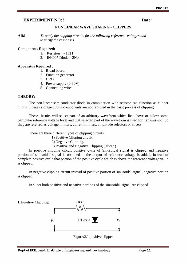
I. Positive Clipping
Figure:2.1.positive clipper
IN 4007
1 KΩ
Vi V0

PDC LAB
Dept of ECE, Lendi Institute of Engineering and Technology Page 12
Figure: 2.2. Input waveform Figure: 2.3.Output waveform.
Vi is a input sinusoidal signal as shown in the figure 2(a) . For positive portion of the
sinusoidal the diode IN4007 gets forward biased. The output voltages in the voltage across the
diode under forward biased which is cut-in-voltage of the diode. Therefore the positive portion
above the cut-in-voltage is clipped or not observed in the output (V0) as shown in figure 2(b).
II. Positive Clipping with Positive Reference Voltage
Figure:2.4. Positive Clipping with Positive Reference Voltage
Figure:2.5.Input waveform Figure:2.6.Output waveform.
The input sinusoidal signal (Vi ) in figure 4(a) can make the diode to conduct when its
instantaneous value is greater than VR. Up to that voltage (VR) the diode is open circuited and the
output voltage is same as the input voltage. After that voltage (VR) the output voltage is VR plus the
cut-in-voltage (V ) of the diode as shown in figure 4(b).
III. Positive Clipping with Negative Reference Voltage
IN 4007
1 KΩ
VR
Vi V0
IN 4007
1 KΩ
VR
Vi V0
Vi
t V
V0
t
Vi
t
VR+ V
V0
t
PDC LAB
Dept of ECE, Lendi Institute of Engineering and Technology Page 13
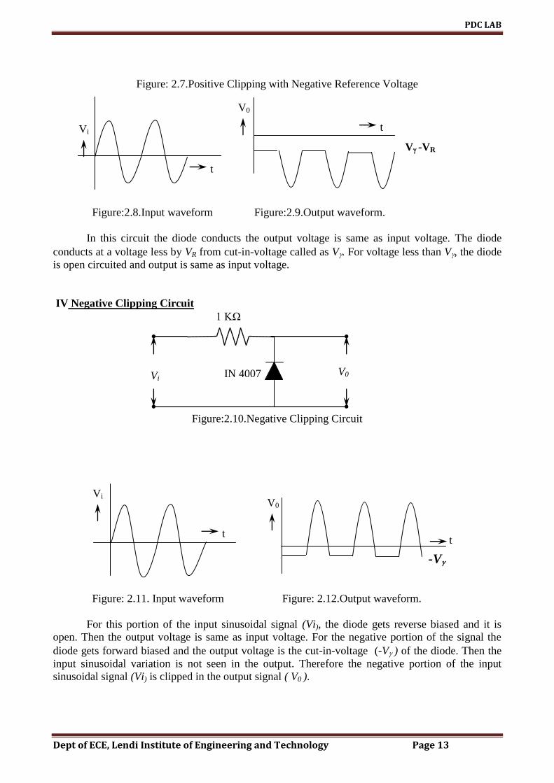
Figure: 2.7.Positive Clipping with Negative Reference Voltage
Figure:2.8.Input waveform Figure:2.9.Output waveform.
In this circuit the diode conducts the output voltage is same as input voltage. The diode
conducts at a voltage less by VR from cut-in-voltage called as V. For voltage less than V, the diode
is open circuited and output is same as input voltage.
IV Negative Clipping Circuit
Figure:2.10.Negative Clipping Circuit
Figure: 2.11. Input waveform Figure: 2.12.Output waveform.
For this portion of the input sinusoidal signal (Vi), the diode gets reverse biased and it is
open. Then the output voltage is same as input voltage. For the negative portion of the signal the
diode gets forward biased and the output voltage is the cut-in-voltage (-V ) of the diode. Then the
input sinusoidal variation is not seen in the output. Therefore the negative portion of the input
sinusoidal signal (Vi) is clipped in the output signal ( V0 ).
V -VR
IN 4007
1 KΩ
Vi V0
Vi
t
V0
t
Vi
t
-V
V0
t

PDC LAB
Dept of ECE, Lendi Institute of Engineering and Technology Page 14
Vi V0
V. Negative Clipping with Negative Reference Voltage
Figure:2.13.Negative Clipping with Negative Reference Voltage
Figure:2.14. Input waveform. Figure:2.15. Output waveform.
In this circuit, the diode gets forward biased for the input sinusoidal voltage is less than (–
VR). For input voltage greater than (–VR), the diode is non-conducting and it is open. Then the
output voltage is same as input voltage.
VI. Negative Clipping with Positive Reference Voltage
Figure:2.16.Negative Clipping with Positive Reference Voltage
Figure: 2.17. Input waveform Figure: 2.18. Output waveform.
IN 4007
1 KΩ
VR
Vi V0
IN 4007
1 KΩ
VR
Vi
t
-VR-V
V0
t
Vi
t VR-V
V0
t

PDC LAB
Dept of ECE, Lendi Institute of Engineering and Technology Page 15
For input sinusoidal signal voltage less than VR, the diode is shorted and the output voltage
is fixed ar VR. For input sinusoidal voltage greater than VR the diode is reverse biased and open
circuited. Then the output voltage is same as input voltage.
VII. Slicer
Vi V0
Figure: 2.19.Slicer
Figure:2.20. Input waveform Figure:2.21.Output waveform.
DESIGN:
1. For positive clipping at „V‟ volts reference select VR = V.
2. For negative clipping at „V‟ volts reference select VR = V.
3. For clipping at two independent levels at V1&V2 reference voltages select
VR1 = V1, VR2 = V2 and VR2 > VR1.
PROCEDURE:
1. Connect the circuit as shown in the figure 1.
2. Connect the function generator at the input terminals and CRO at the output
terminals of the circuit.
3. Apply a sine wave signal of frequency 1KHz at the input and observe the output
waveforms of the circuits.
4. Repeat the procedure for figure 3, 5, 7, 9, 11 and 13.
RESULT:
V =
Clipping circuits for different reference voltages are studied.
VIVA QUESTIONS:
1. Define clipping? Describe (i) Positive clipper (ii) Biased clipper
(iii) Combination clipper.
2. Define clamping?
3. Define peak inverse voltage of diode?
4. What are the other names for the clamper?
5. What are the applications of clampers?
IN 4007
1 KΩ
VR1
IN 4007
VR2
Vi
t V+VR
V-VR
V0
t

PDC LAB
Dept of ECE, Lendi Institute of Engineering and Technology Page 16
6. Explain the clipping process?
7. Discuss the differences between shunt and series clipper.
8. Draw the o/p waveforms for
i) Series diode +ve clipper
ii) Series diode -ve clipper
iii) Shunt diode +ve clipper
iv) Shunt diode -ve clipper
v) Two level clipper
9. Draw the o/p wave forms for
i). +ve clamper
ii). –ve clamper
APPLICATIONS:
1. Used in radars, digital computers and other electronic systems for removing unwanted portions of
the input signal voltages above or below a specified level.
2. used in radio-receivers for communication circuits where noise pulses that rise well above the
signal amplitude are clipped down to the desired level.
DESIGNING PROBLEM:
1. The circuit shown in Figure below is used to “square” a 1Khz input sine wave whose peak is
40V. It is desired that the output voltage waveform be flat for 90% of time. Find the values
if VR1 and VR2. Assume ideal diodes. At what value of input will the waveform be clipped?
Input waveform Output waveform.

PDC LAB
Dept of ECE, Lendi Institute of Engineering and Technology Page 17
GRAPH

PDC LAB
Dept of ECE, Lendi Institute of Engineering and Technology Page 18
GRAPH
PDC LAB
Dept of ECE, Lendi Institute of Engineering and Technology Page 19
EXPERIMENT NO:3 Date:
NON LINEAR WAVE SHAPING – CLAMPERS
AIM : To get positive and negative clamping for sinusoidal and Square
wave inputs.
COMPONENTS REQUIRED:
1. Resistors - 1k
2. IN4007 Diode
3. Capacitor -10F
APPARATUS REQUIRED:
1. Bread board
2. Function generator
3. CRO
4. Power supply 0-30V
5. Connecting Wires.
THEORY:
Clamping Circuit
“A clamping circuit is one that takes an input waveform and provides an output that is a
faithful replica of its shape but has one edge tightly clamped to the zero voltage reference point”.
There are various types of Clamping circuits, which are mentioned below:
1. Positive Clamping Circuit.
2. Negative Clamping Circuit.
3. Positive Clamping with positive reference voltage.
4. Negative Clamping with positive reference voltage.
5. Positive Clamping with negative reference voltage.
6. Negative Clamping with negative reference voltage.
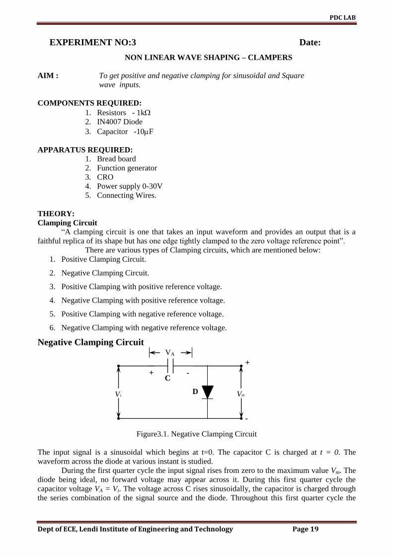
Negative Clamping Circuit
Figure3.1. Negative Clamping Circuit
The input signal is a sinusoidal which begins at t=0. The capacitor C is charged at t = 0. The
waveform across the diode at various instant is studied.
During the first quarter cycle the input signal rises from zero to the maximum value Vm. The
diode being ideal, no forward voltage may appear across it. During this first quarter cycle the
capacitor voltage VA = Vi. The voltage across C rises sinusoidally, the capacitor is charged through
the series combination of the signal source and the diode. Throughout this first quarter cycle the
Vi V0
VA
C
D
+ -
+
-
PDC LAB
Dept of ECE, Lendi Institute of Engineering and Technology Page 20
mi VVV 0
output V0 has remained zero. At the end of this quarter cycle there exists across the capacitor a
voltage VA = Vm.
After the first quarter cycle, the peak has been passed and the input signal begins to fall, the
voltage VA across the capacitor is no longer able to follow the input voltage. For in order to do so, it
would be required that the capacitor discharge, and because of the diode, such a discharge is not
possible. The capacitor remains charged to the voltage VA = Vm, and, after the first quarter cycle the
output is V0 = Vi – Vm. During succeeding cycles the positive excursion of the signal just barely
reaches zero. The diode need never again conduct, and the positive extremity of the signal has been
clamped to zero. The average value of the signal is –Vm.
Positive Clamping Circuit:
Figure3.2. Positive Clamping Circuit
It is also called as negative peak clamper, because this circuit clamps at the negative peaks of a
signal.
Let the input signal be Vi = Vm sint. When Vi goes negative, diode gets forward biased and
conducts. The capacitor charges to voltage Vm, with polarity as shown. Under steady state
condition, the positive clamping circuit is given as,
)(0 mi VVV
Eq.1
During the negative half cycle of Vi, the diode conducts and C charges to –Vm volts, i.e., the
negative peak value. The capacitor cannot discharge since the diode cannot conduct in the reverse
direction. Thus the capacitor acts as a battery of –Vm volts and the output voltage is given by
equation.1 above. It is seen for figure 2, that the negative peaks of the input signal are clamped to
zero level. Peak-to-peak amplitude of output voltage 2Vm, which is the same as that of the input
signal.
Negative Clamping with Positive Reference Voltage
Vi V0
C
D
VR
Vi V0
Vm
C
D
+ -
+
-
+
-
PDC LAB
Dept of ECE, Lendi Institute of Engineering and Technology Page 21
Figure:3.3. Negative Clamping with Positive Reference Voltage
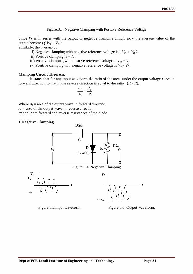
Since VR is in series with the output of negative clamping circuit, now the average value of the
output becomes (-Vm + VR ).
Similarly, the average of
i) Negative clamping with negative reference voltage is (-Vm + VR ).
ii) Positive clamping is +Vm.
iii) Positive clamping with positive reference voltage is Vm + VR.
iv) Positive clamping with negative reference voltage is Vm - VR.
Clamping Circuit Theorem:
It states that for any input waveform the ratio of the areas under the output voltage curve in
forward direction to that in the reverse direction is equal to the ratio (Rf / R).
R
R
A
A f
r
f .
Where Af = area of the output wave in forward direction.
Ar = area of the output wave in reverse direction.
Rf and R are forward and reverse resistances of the diode.
I. Negative Clamping
Figure:3.4. Negative Clamping
Figure:3.5.Input waveform Figure:3.6. Output waveform.
IN 4007
1 KΩ Vi V0
10F
C
D R
Vi
t
Vm
-Vm
V0
t
-2Vm

PDC LAB
Dept of ECE, Lendi Institute of Engineering and Technology Page 22
II. Negative Clamping with Positive Reference Voltage.
Figure:3.7. Negative Clamping with Positive Reference Voltage
Figure:3.8.Input waveform Figure:3.9.Output waveform.
III. Negative Clamping with Negative Reference Voltage.
Figure:3.10. Negative Clamping with Negative Reference Voltage
Figure:3.11.Input waveform Figure:3.12 Output waveform.
IN 4007
1 KΩ
Vi V0
10F
C
D
R
VR
t
Vi VR
t
V0
t t
V0 Vi
-VR
IN 4007
1 KΩ
Vi V0
10F
C
D
R
VR

PDC LAB
Dept of ECE, Lendi Institute of Engineering and Technology Page 23
IV. Positive Clamping.
figure:3.13.Positive Clamping
Figure:3.14.Input waveform Figure:3.15. Output waveform.
V. Positive Clamping with Negative Reference Voltage.
Figure: 3.16. Positive Clamping with Negative Reference Voltage
Figure:3.17.Input waveform Figure:3.18. Output waveform.
VI. Positive Clamping with Positive reference Voltage.
IN 4007
1 KΩ Vi V0
10F
C
D R
IN 4007
1 KΩ
Vi V0
10F
C
D
R
VR
t
Vi
t
V0 -VR
V0
t
Vi
t
2Vm
Vm
-Vm
PDC LAB
Dept of ECE, Lendi Institute of Engineering and Technology Page 24
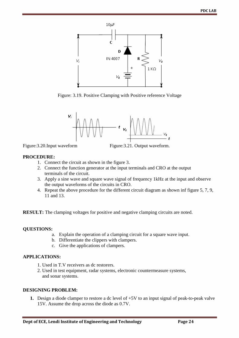
Figure: 3.19. Positive Clamping with Positive reference Voltage
Figure:3.20.Input waveform Figure:3.21. Output waveform.
PROCEDURE:
1. Connect the circuit as shown in the figure 3.
2. Connect the function generator at the input terminals and CRO at the output
terminals of the circuit.
3. Apply a sine wave and square wave signal of frequency 1kHz at the input and observe
the output waveforms of the circuits in CRO.
4. Repeat the above procedure for the different circuit diagram as shown inf figure 5, 7, 9,
11 and 13.
RESULT: The clamping voltages for positive and negative clamping circuits are noted.
QUESTIONS:
a. Explain the operation of a clamping circuit for a square wave input.
b. Differentiate the clippers with clampers.
c. Give the applications of clampers.
APPLICATIONS:
1. Used in T.V receivers as dc restorers.
2. Used in test equipment, radar systems, electronic countermeasure systems,
and sonar systems.
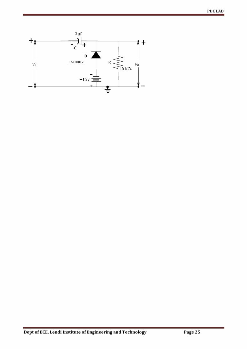
DESIGNING PROBLEM:
1. Design a diode clamper to restore a dc level of +5V to an input signal of peak-to-peak valve
15V. Assume the drop across the diode as 0.7V.
PDC LAB
Dept of ECE, Lendi Institute of Engineering and Technology Page 25

PDC LAB
Dept of ECE, Lendi Institute of Engineering and Technology Page 26
GRAPH

PDC LAB
Dept of ECE, Lendi Institute of Engineering and Technology Page 27
GRAPH

PDC LAB
Dept of ECE, Lendi Institute of Engineering and Technology Page 28
GRAPH

PDC LAB
Dept of ECE, Lendi Institute of Engineering and Technology Page 29
EXPERIMENT NO:4 Date:
TRANSISTOR AS A SWITCH
AIM : To design and observe the performance of a transistor as a switch.
COMPONENTS REQUIRED :
1. Resistors
2. LED
3. 2N2369 Transistor
APPARATUS REQUIRED:
1. Bread board
2. Function generator 1Hz- 1MHz
3. CRO 1Hz -20MHz
4. Power supply 0-30V
THEORY:
Transistors are widely used in digital logic circuits and switching applications.in these
applications the voltage levels periodically alternate between a “LOW” and a “HIGH”
voltage,such as 0v and +5v.in switching circuits ,a transistor is operated at cutoff for the off
condition ,ans the saturation for the ON condition.the active linear region is passed through
abruptly from cutoff to saturation or vice versa.in cut off region,both the transistor junctions
between Emitter and Base and the junction between base and collector are reverse biased and only
the reverse current which is very small and practically neglected,flows in the transistor.in
saturation region both junctions are in forward bais and the values of Vce (sat) and Vbe(sat) are small.
CIRCUIT DIAGRAM:
Figure 4.1.circuit diagram of transistor working as a switch

PDC LAB
Dept of ECE, Lendi Institute of Engineering and Technology Page 30
PROCEDURE:
1.Connect the circuit as per circuit diagram.
2.Obtain a constant amplitude square wave from function generator of 5V p-p and give
the signal as input to the circuit.
4.Draw the input and output waveforms
3.Observe the output waveform and note down its voltage amplitude levels.
MODEL WAVEFORM:
Figure4.2.model waveforms
OBSERVATIONS:
THEORETICAL CALCULATIONS:
When Vi=+2.5v,the transistor goes into saturation region .
So Vout=Vce (sat)=0.3V.
When Vi=-2.5v,the transistor goes into cutoff region .
So Vout=Vcc =5v
PRECAUTIONS:
1. Connections should be made carefully.
2. Verify the circuit before giving supply voltage.
3. Take reading without any parallax error.
PDC LAB
Dept of ECE, Lendi Institute of Engineering and Technology Page 31
RESULT:
Switchinng charactristics of a transistor are observed.
VIVA QUESTIONS:
1. What are the three regions of operation of a transistor.
2. What do you mean by time delay of a transistor.
3. When does the transistor acts as (a) a closed switch (b) an open switch.
4. How are the junctions of a transistor biased for a active region operation.
5. What do you mean by turn ON time of a transistor.
APPLICATIONS:
Used for switching purpose in analog and digital communication networks.
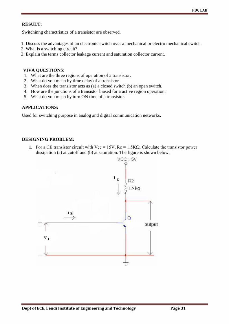
DESIGNING PROBLEM:
1. For a CE transistor circuit with Vcc = 15V, Rc = 1.5KΩ. Calculate the transistor power
dissipation (a) at cutoff and (b) at saturation. The figure is shown below.
1. Discuss the advantages of an electronic switch over a mechanical or electro mechanical switch.
2. What is a switching circuit?
3. Explain the terms collector leakage current and saturation collector current.

PDC LAB
Dept of ECE, Lendi Institute of Engineering and Technology Page 32

PDC LAB
Dept of ECE, Lendi Institute of Engineering and Technology Page 33
GRAPH
PDC LAB
Dept of ECE, Lendi Institute of Engineering and Technology Page 34
EXPERIMENT NO: 5 Date:
STUDY OF LOGIC GATES
AIM : To study the various logic gates by using discrete components.
COMPONENTS REQUIRED :
1. Resistors - 1k -1, 10 k -2
2. IN4007 Diode – 2 no
3. Transistor 2N2369
APPARATUS REQUIRED:
1. Power supply 0-30V
2. Bread board
3. Connecting wires
THEORY:
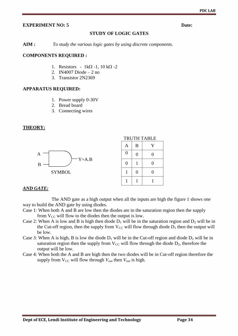
TRUTH TABLE
A B Y
0 0 0
0 1 0
1 0 0
1 1 1
AND GATE:
The AND gate as a high output when all the inputs are high the figure 1 shows one
way to build the AND gate by using diodes.
Case 1: When both A and B are low then the diodes are in the saturation region then the supply
from VCC will flow to the diodes then the output is low.
Case 2: When A is low and B is high then diode D1 will be in the saturation region and D2 will be in
the Cut-off region, then the supply from VCC will flow through diode D1 then the output will
be low.
Case 3: When A is high, B is low the diode D1 will be in the Cut-off region and diode D2 will be in
saturation region then the supply from VCC will flow through the diode D2, therefore the
output will be low.
Case 4: When both the A and B are high then the two diodes will be in Cut-off region therefore the
supply from VCC will flow through Vout then Vout is high.
A
B Y=A.B
SYMBOL

PDC LAB
Dept of ECE, Lendi Institute of Engineering and Technology Page 35
OR GATE:
TRUTH TABLE
A B Y
0 0 0
0 1 1
1 0 1
1 1 1
An OR gate has two or more inputs but only one output signal. It is called OR gate because
the output voltage is high if any or all the inputs are high.
The figure 2 shows one way to build OR gate (two inputs) by using diodes.
Case 1: When A and B are low then the two diodes D1 and D2 are in Cut-off region. Then the Vout
is low.
Case 2: When A is low and B is high then the diode D1 is in Cut-off region and diode D2 is in
saturation region, then the Vout is high.
Case 3: When A is high and B is low then the diode D2 is in saturation region and diode D1 is in
Cut-off region, then the Vout is high.
Case 4: When both A and B are high the diodes D1 and D2 are in saturation region then the output
Vout is high.
NOR GATE:
TRUTH TABLE
Symbol
NOR gate is referred to a NOT OR gate because the output is BAY . Read this as Y =
NOT A OR B or Y = compliment of the A OR B. the circuit is in an OR gate followed by a NO
gate OR inverter. The only to get high output is to have both inputs low.
A B Y
0 0 1
0 1 0
1 0 0
1 1 0
A
B Y = A + B
SYMBOL
A
B
Y = A + B BAY
A
B BAY
PDC LAB
Dept of ECE, Lendi Institute of Engineering and Technology Page 36
A
B
Y = A.B BAY .
A
B BAY .
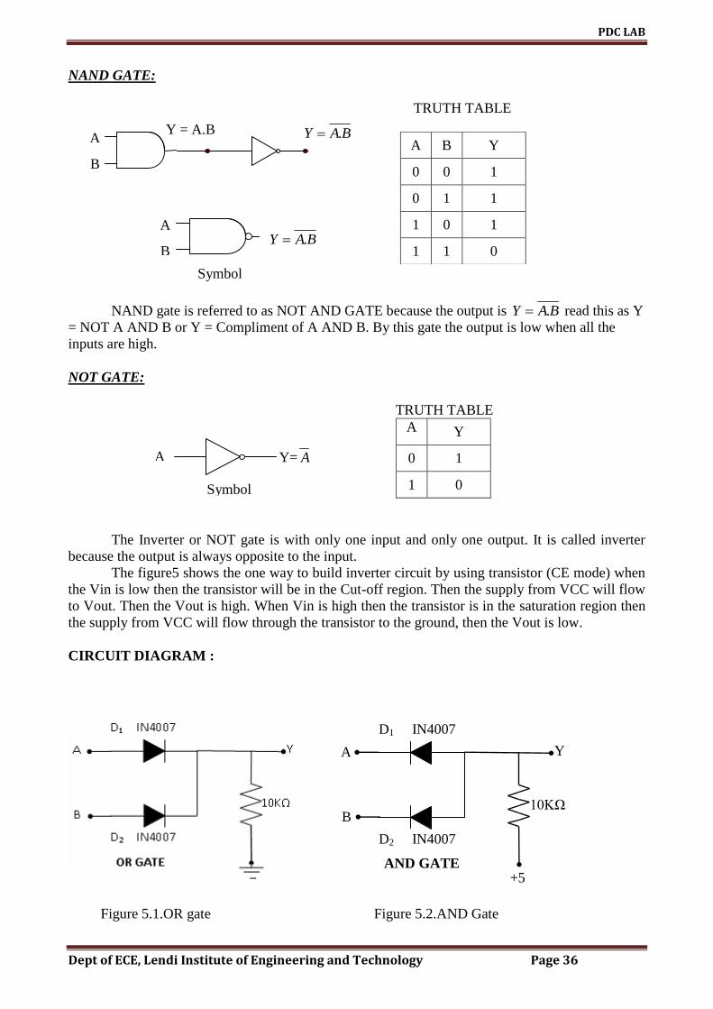
NAND GATE:
TRUTH TABLE
Symbol
NAND gate is referred to as NOT AND GATE because the output is BAY . read this as Y
= NOT A AND B or Y = Compliment of A AND B. By this gate the output is low when all the
inputs are high.
NOT GATE:
TRUTH TABLE
A Y
0 1
1 0
The Inverter or NOT gate is with only one input and only one output. It is called inverter
because the output is always opposite to the input.
The figure5 shows the one way to build inverter circuit by using transistor (CE mode) when
the Vin is low then the transistor will be in the Cut-off region. Then the supply from VCC will flow
to Vout. Then the Vout is high. When Vin is high then the transistor is in the saturation region then
the supply from VCC will flow through the transistor to the ground, then the Vout is low.
CIRCUIT DIAGRAM :
Figure 5.1.OR gate Figure 5.2.AND Gate
A B Y
0 0 1
0 1 1
1 0 1
1 1 0
D1 IN4007
D2 IN4007
10KΩ
Y A
B
+5 AND GATE
A Y= A
Symbol

PDC LAB
Dept of ECE, Lendi Institute of Engineering and Technology Page 37
Figure 5.3.NOR Gate
Figure 5.4.NAND Gate
Figure 5.5.NOT Gate
PROCEDURE:
1. Connect the circuit as shown in figures above.
2. Verify the truth tables of various gates for different conditions of inputs.
3. Repeat the steps 1&2 for figures 2, 3, 4 & 5.
D1
IN4007
D2
IN4007
10K
Ω
Y
A
B
+5
NOR
GATE
1KΩ
10K
Ω
2N2369
D1 IN4007
D2 IN4007
10KΩ
Y
A
B
VCC +5V
NAND GATE
1KΩ
10KΩ
2N2369
+5
1KΩ
Y
2N2369 A NOT GATE
10KΩ

PDC LAB
Dept of ECE, Lendi Institute of Engineering and Technology Page 38
TRUTH TABLES:
AND GATE OR GATE NAND GATE NOR GATE NOT GATE
A B Y A B Y A B Y A B Y A Y
0
0
1
1
0
1
0
1
0
0
1
1
0
1
0
1
0
0
1
1
0
1
0
1
0
0
1
1
0
1
0
1
0
1
1
0
Where 5V is represented by logic 1.
RESULT: Different logic gates are studied and their truth tables are verified .
QUESTIONS:
1. Realize AND, OR, NOT gates using NAND & NOR gates
2. Why NAND & NOR gates are called universal gates.
APPLICATIONS:
1. Arithmetic adders, multiplexers, and some kinds of memories.
2. Computers,arger components like Internet routers, digital television sets, your cell
phone, tablet, Blue Ray player, or iPad.

PDC LAB
Dept of ECE, Lendi Institute of Engineering and Technology Page 39
GRAPH
PDC LAB
Dept of ECE, Lendi Institute of Engineering and Technology Page 40
EXPERIMENT NO:6 Date:
STUDY OF FLIP-FLOPS
AIM: to verify the truth table of SR latch ,JK flipflop ,JK master slave flipflop,T-flipflop and D-
flipflop.
COMPONENTS REQUIRED:
1. IC 74LS00
2. IC 74LS10
3. IC 74LS04.
4. Digital Trainer Kit.
THEORY:
RS FLOP-FLOP:
Consider the logic Symbol for RS flip-flop shown in Fig. Notice that the RS flip-flop has two
inputs, labeled S and R. The two outputs are labeled Q and Q . Note that the outputs are always
opposite, or complementary in the flip-flops.
Fig 6.1 shows the timing diagram for an RS flip-flop. Notice that the output Q goes high
whenever R goes low; and the output Q goes LOW whenever S goes LOW. The logic levels (0,1)
are on the left side of the wave forms. The output Q „holds‟ whenever the both inputs are high.
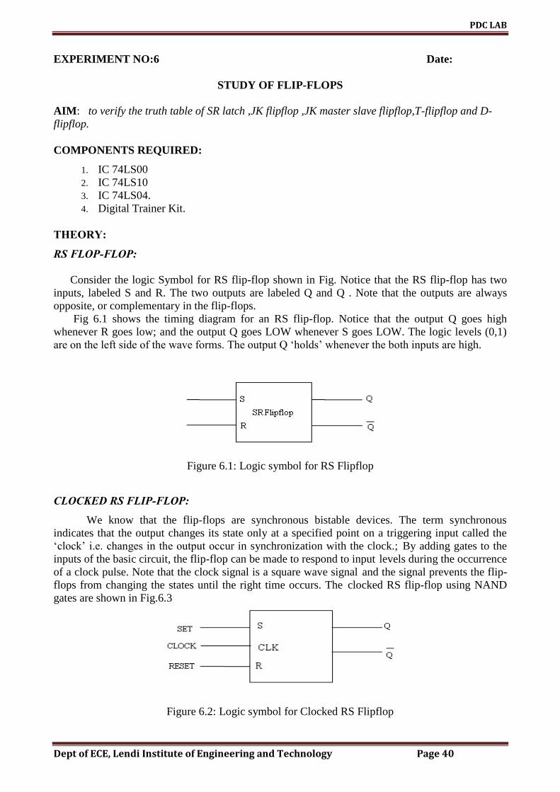
Figure 6.1: Logic symbol for RS Flipflop
CLOCKED RS FLIP-FLOP:
We know that the flip-flops are synchronous bistable devices. The term synchronous indicates that the output changes its state only at a specified point on a triggering input called the „clock‟ i.e. changes in the output occur in synchronization with the clock.; By adding gates to the
inputs of the basic circuit, the flip-flop can be made to respond to input levels during the occurrence
of a clock pulse. Note that the clock signal is a square wave signal and the signal prevents the flip-
flops from changing the states until the right time occurs. The clocked RS flip-flop using NAND
gates are shown in Fig.6.3
Figure 6.2: Logic symbol for Clocked RS Flipflop
PDC LAB
Dept of ECE, Lendi Institute of Engineering and Technology Page 41
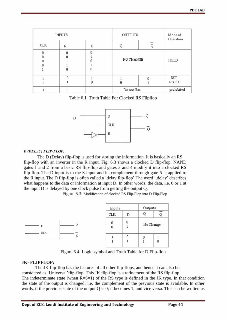
Table 6.1. Truth Table For Clocked RS Flipflop
Figure 6.3: Modification of clocked RS Flip-Flop into D Flip-Flop
Figure 6.4: Logic symbol and Truth Table for D Flip-flop
JK- FLIPFLOP:
The JK flip-flop has the features of all other flip-flops, and hence it can also be
considered as „Universal‟flip-flop. This JK flip-flop is a refinement of the RS flip-flop.
The indeterminate state (when R=S=1) of the RS type is defined in the JK type. In that condition
the state of the output is changed; i.e. the complement of the previous state is available. In other
words, if the previous state of the output Q is 0; it becomes 1; and vice versa. This can be written as
D (DELAY) FLIP-FLOP:
The D (Delay) flip-flop is used for storing the information. It is basically an RS
flip-flop with an inverter in the R input. Fig. 6.3 shows a clocked D flip-flop. NAND
gates 1 and 2 from a basic RS flip-flop and gates 3 and 4 modify it into a clocked RS
flip-flop. The D input is to the S input and its complement through gate 5 is applied to
the R input. The D flip-flop is often called a „delay flip-flop‟ The word „.delay‟ describes
what happens to the data or information at input D. In other words, the data, i.e. 0 or 1 at
the input D is delayed by one clock pulse from getting the output Q.
PDC LAB
Dept of ECE, Lendi Institute of Engineering and Technology Page 42
Qn+1 = complement Qn.
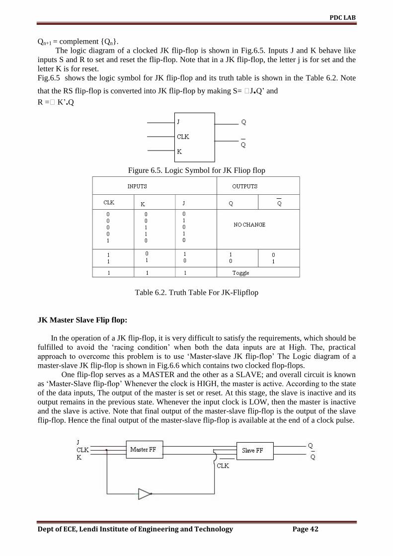
The logic diagram of a clocked JK flip-flop is shown in Fig.6.5. Inputs J and K behave like
inputs S and R to set and reset the flip-flop. Note that in a JK flip-flop, the letter j is for set and the
letter K is for reset.
Fig.6.5 shows the logic symbol for JK flip-flop and its truth table is shown in the Table 6.2. Note
that the RS flip-flop is converted into JK flip-flop by making S= J.Q‟ and
R = K‟.Q
Figure 6.5. Logic Symbol for JK Fliop flop
Table 6.2. Truth Table For JK-Flipflop
JK Master Slave Flip flop:
In the operation of a JK flip-flop, it is very difficult to satisfy the requirements, which should be
fulfilled to avoid the „racing condition‟ when both the data inputs are at High. The, practical
approach to overcome this problem is to use „Master-slave JK flip-flop‟ The Logic diagram of a
master-slave JK flip-flop is shown in Fig.6.6 which contains two clocked flop-flops. One flip-flop serves as a MASTER and the other as a SLAVE; and overall circuit is known
as „Master-Slave flip-flop‟ Whenever the clock is HIGH, the master is active. According to the state
of the data inputs, The output of the master is set or reset. At this stage, the slave is inactive and its
output remains in the previous state. Whenever the input clock is LOW, then the master is inactive
and the slave is active. Note that final output of the master-slave flip-flop is the output of the slave
flip-flop. Hence the final output of the master-slave flip-flop is available at the end of a clock pulse.

PDC LAB
Dept of ECE, Lendi Institute of Engineering and Technology Page 43
Figure 6.6: Logic Diagram Of Master-Slave J-K Flip-Flop
T(TOGGLE) FLIP FLOP:
The single input version of the JK flip-flop is (toggle) flip-flop and it is obtained from a JK
flip-flop if both inputs are tied together. The name T comes from the ability of the flip-flop to
„toggle‟ or change the state. Generally T flip-flop IC‟ are not available. It can be realized using JK,
SR, or D flip-flop.
Fig 6.7. shows the logic diagram of a clocked T flip-flop; which has only one input
referred to as T-input.
Figure 6.7: Logic symbol and Truth Table for T Flip-flop

PDC LAB
Dept of ECE, Lendi Institute of Engineering and Technology Page 44
CIRCUIT DIAGRAMS:
PROCEDURE:
1. Connect the circuit diagram as shown in the diagram.
2. Verify the truth table of the SR latch.
3. Connect the JK flip-flop circuit using 3-input NAND gates and verify the truth table.
4. Verify the truth table for T and D Flip-flops.

PDC LAB
Dept of ECE, Lendi Institute of Engineering and Technology Page 45
5. Verify the truth table for J-K MASTER-SLAVE FLIP-FLOP
QUESTIONS:
1. What is a sequential logic circuit? How is it different from a combinational system?
2. What is a binary? What is a flip-flop?
3. Explain the meaning of set and reset?
4. Explain the need of flip-flop?
5. What basic purpose does all flip-flops serve?
6. Is it possible to toggle a SR flip-flop? Explain?
7. Explain the meaning of race – around problem? How does it affect the behavior of a
flip-flop?
8. Explain how the race – around problem is overcome in the JK Master Slave flip flop
9. Explain how a shift register can be constructed from SR flip-flop?
APPLICATIONS:
1. Data Storage
2. Data Transfer
3. Counters
4. Frequency division

PDC LAB
Dept of ECE, Lendi Institute of Engineering and Technology Page 46
GRAPH
PDC LAB
Dept of ECE, Lendi Institute of Engineering and Technology Page 47
EXPERIMENT NO:7 Date:
BISTABLE MULTIVIBRATOR
AIM: To design a fixed bias Bistable Multivibrator and to measure the stable state
voltages before and after triggering.
COMPONENTS REQUIRED:
1. Resistors 2.2KΩ-2
15 KΩ-2
100 KΩ-2
2. Transistors 2N2369 – 2
APPARATUS: 1. Bread board
2. Power supply 0-30V
3. CRO
4. Connecting wires
THEORY:
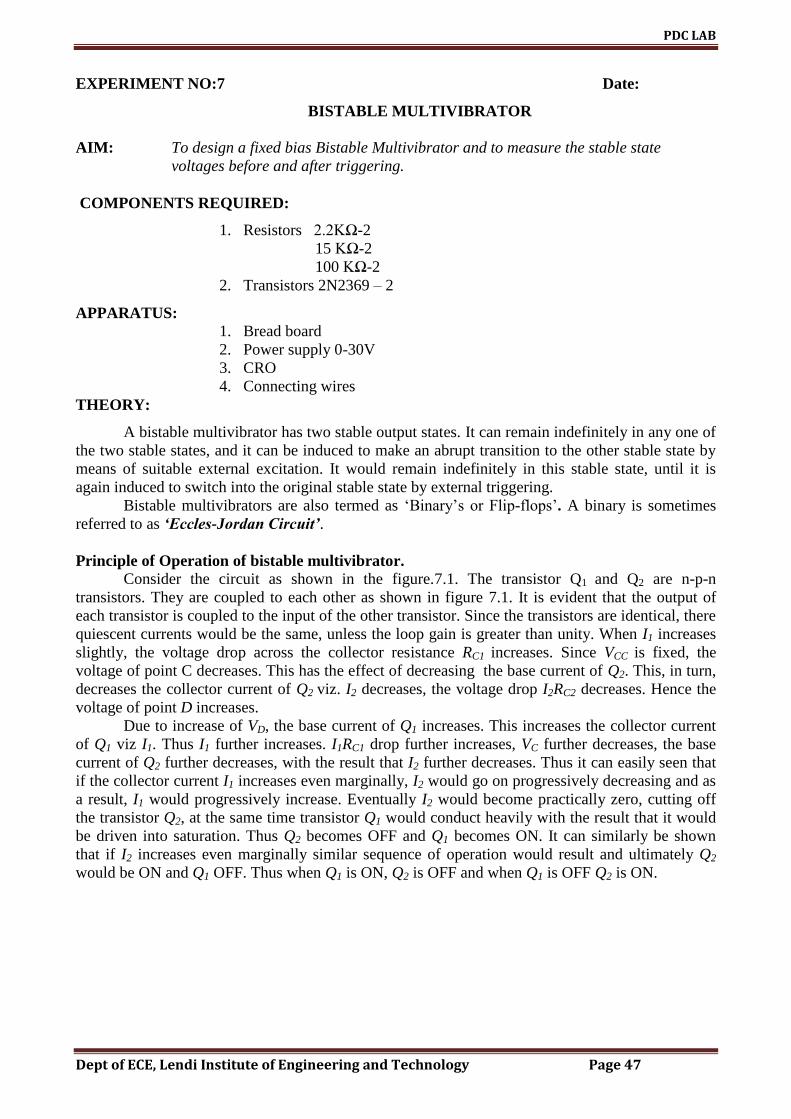
A bistable multivibrator has two stable output states. It can remain indefinitely in any one of
the two stable states, and it can be induced to make an abrupt transition to the other stable state by
means of suitable external excitation. It would remain indefinitely in this stable state, until it is
again induced to switch into the original stable state by external triggering.
Bistable multivibrators are also termed as „Binary‟s or Flip-flops‟. A binary is sometimes
referred to as ‘Eccles-Jordan Circuit’.
Principle of Operation of bistable multivibrator.
Consider the circuit as shown in the figure.7.1. The transistor Q1 and Q2 are n-p-n
transistors. They are coupled to each other as shown in figure 7.1. It is evident that the output of
each transistor is coupled to the input of the other transistor. Since the transistors are identical, there
quiescent currents would be the same, unless the loop gain is greater than unity. When I1 increases
slightly, the voltage drop across the collector resistance RC1 increases. Since VCC is fixed, the
voltage of point C decreases. This has the effect of decreasing the base current of Q2. This, in turn,
decreases the collector current of Q2 viz. I2 decreases, the voltage drop I2RC2 decreases. Hence the
voltage of point D increases.
Due to increase of VD, the base current of Q1 increases. This increases the collector current
of Q1 viz I1. Thus I1 further increases. I1RC1 drop further increases, VC further decreases, the base
current of Q2 further decreases, with the result that I2 further decreases. Thus it can easily seen that
if the collector current I1 increases even marginally, I2 would go on progressively decreasing and as
a result, I1 would progressively increase. Eventually I2 would become practically zero, cutting off
the transistor Q2, at the same time transistor Q1 would conduct heavily with the result that it would
be driven into saturation. Thus Q2 becomes OFF and Q1 becomes ON. It can similarly be shown
that if I2 increases even marginally similar sequence of operation would result and ultimately Q2
would be ON and Q1 OFF. Thus when Q1 is ON, Q2 is OFF and when Q1 is OFF Q2 is ON.
PDC LAB
Dept of ECE, Lendi Institute of Engineering and Technology Page 48
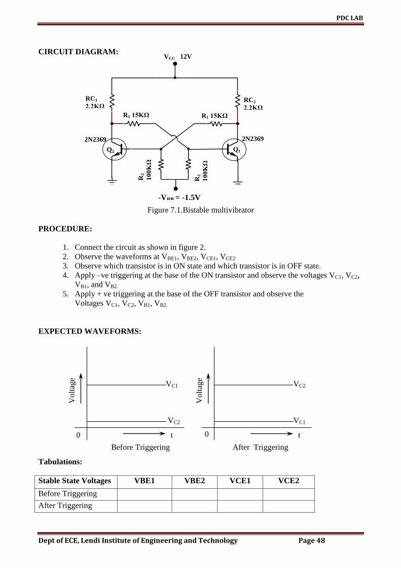
CIRCUIT DIAGRAM:
Figure 7.1.Bistable multivibrator
PROCEDURE:
1. Connect the circuit as shown in figure 2.
2. Observe the waveforms at VBE1, VBE2, VCE1, VCE2
3. Observe which transistor is in ON state and which transistor is in OFF state.
4. Apply –ve triggering at the base of the ON transistor and observe the voltages VC1, VC2,
VB1, and VB2.
5. Apply + ve triggering at the base of the OFF transistor and observe the
Voltages VC1, VC2, VB1, VB2.
EXPECTED WAVEFORMS:
Tabulations:
Stable State Voltages VBE1 VBE2 VCE1 VCE2
Before Triggering
After Triggering
t
Volt
age
VC1
VC2
Before Triggering
t
Volt
age
VC1
VC2
After Triggering
0 0
RC1
2.2KΩ RC2
2.2KΩ R1 15KΩ
2N2369 2N2369
VCC 12V
-VBB = -1.5V
R1 15KΩ
R2
100KΩ
R2
100KΩ
Q1 Q2

PDC LAB
Dept of ECE, Lendi Institute of Engineering and Technology Page 49
RESULT:
Hence we have designed a fixed bias Bistable Multivibrator and measured the
Stable state voltages before and after triggering.
QUESTIONS:
1. What is Multivibrator? Explain the principle on which it works? Why is it called a
binary?
2. Explain the role of commutating capacitors in a Bistable Multivibrator?
3. Give the Application of a Binary.
APPLICATIONS:
1. used for the performance of many digital operations such as counting and storing binary
information.
2. used in the generation and processing of pulse-type waveforms.
DESIGNING PROBLEM:
1. Silicon transistors with hfe(min) equal to 20 are available. If Vcc=VBB = 10V, design the
bistable multivibrator.

PDC LAB
Dept of ECE, Lendi Institute of Engineering and Technology Page 50
GRAPH
PDC LAB
Dept of ECE, Lendi Institute of Engineering and Technology Page 51
EXPERIMENT NO:8 Date:
ASTABLE MULTIVIBRATOR
AIM : To design and test performance of an Astable Multivibrator to generate clockpulse for a
given frequency.
COMPONENTS REQUIRED:
1. Resistors 3.3KΩ-2
10KΩ-2
2. Capacitors 0.1 f - 2
3. Transistors 2N2369 – 2
APPARATUS :
1. CRO
2. Power supply 0-30V
3. Bread board
4. Connecting wires
THEORY:
An Astable multivibrator has two quasi-stable states, and it keeps on switching between
these two states, by itself, No external triggering signal is needed. The astable multivibrator cannot
remain indefinitely in any of these two states. The two amplifiers of an astable multivibrator are
regeneratively cross-coupled by capacitor.
Principle:
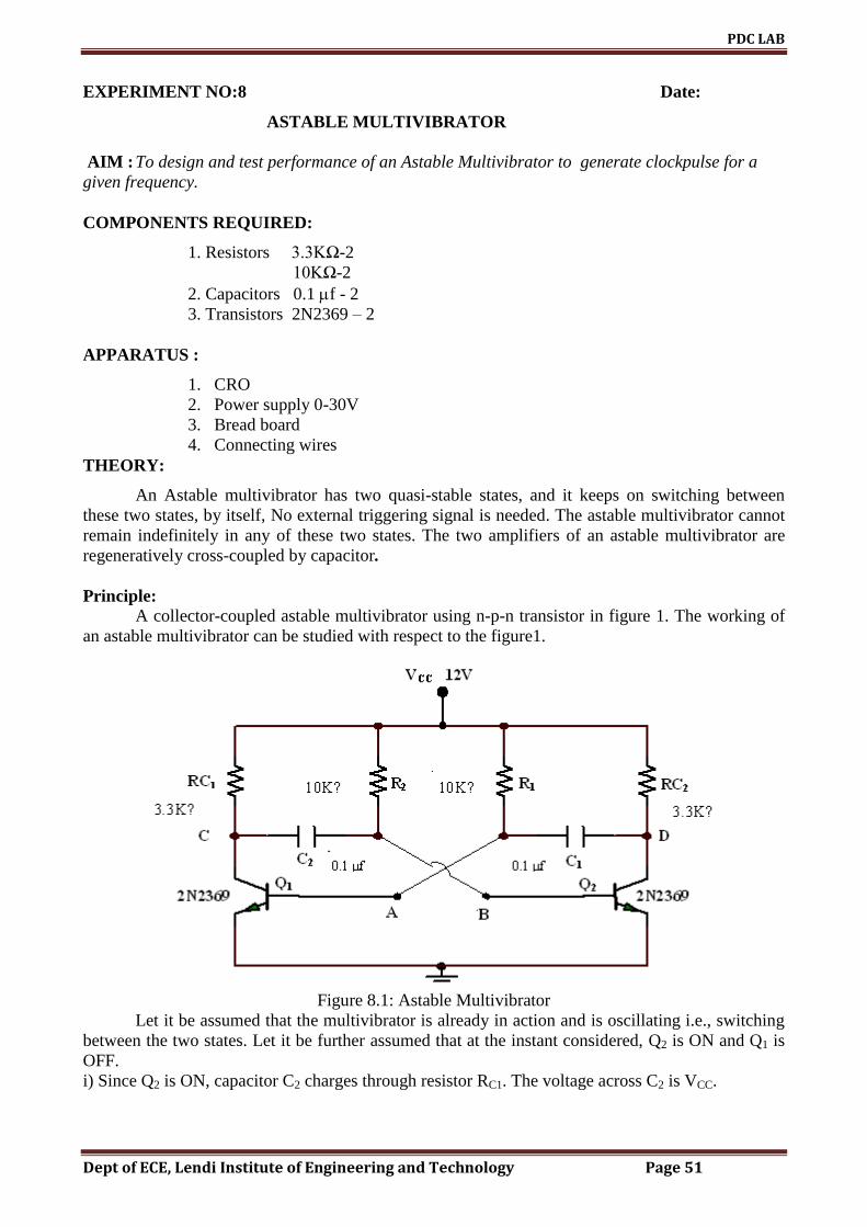
A collector-coupled astable multivibrator using n-p-n transistor in figure 1. The working of
an astable multivibrator can be studied with respect to the figure1.
Figure 8.1: Astable Multivibrator
Let it be assumed that the multivibrator is already in action and is oscillating i.e., switching
between the two states. Let it be further assumed that at the instant considered, Q2 is ON and Q1 is
OFF.
i) Since Q2 is ON, capacitor C2 charges through resistor RC1. The voltage across C2 is VCC.

PDC LAB
Dept of ECE, Lendi Institute of Engineering and Technology Page 52
ii) Capacitor C1discharges through resistor R1, the voltage across C1 when it is about to start
discharging is VCC.(Capacitor C1 gets charged to VCC when Q1 is ON).
As capacitor C1 discharges more and more, the potential of point A becomes more and more
positive (or less and less negative), and eventually VA becomes equal to V, the cut in voltage of
Q1. For VA > V, transistor Q1 starts conducting. When Q1 is ON Q2 becomes OFF.
Similar operations repeat when Q1 becomes ON and Q2 becomes OFF.
Thus with Q1 ON and Q2 OFF, capacitor C1 charges through resistor RC2 and capacitor C2
discharges through resistor R2. As capacitor C2 discharges more and more , it is seen that the
potential of point B becomes less and less negative (or more and more positive), and eventually VB
becomes equal to V, the cut in voltage of Q2. when VB > V, transistor Q2 starts conducting. When
Q2 becomes On, Q1 becomes OFF.
It is thus seen that the circuit keeps on switching continuously between the two quasi-stable
states and once in operation, no external triggering is needed. Square wave voltage are generated at
the collector terminals of Q1 and Q2 i.e., at points C and D.
DESIGN:
IC max = 5 mA ; VCC = 12 V; VCE (SAT) = 0.2V
RC = (VCC - VCE(SAT)) / IC MAX
Let C = 0.1 f
and R= 10K
T = 0.69 (R1C1+R2C2) = 0.69(2RC) ( R1=R2 ; C1=C2)
=TON+TOFF
PROCEDURE:
1. Connect the circuit as shown in figure 1.
2. Observe the waveforms at VBE1, VBE2, VCE1, VCE2 and find frequency.
3. Vary C from 0.01 to 0.001F and measure the frequency at each step.
4. Keep the DC- AC control of the Oscilloscope in DC mode.
PDC LAB
Dept of ECE, Lendi Institute of Engineering and Technology Page 53
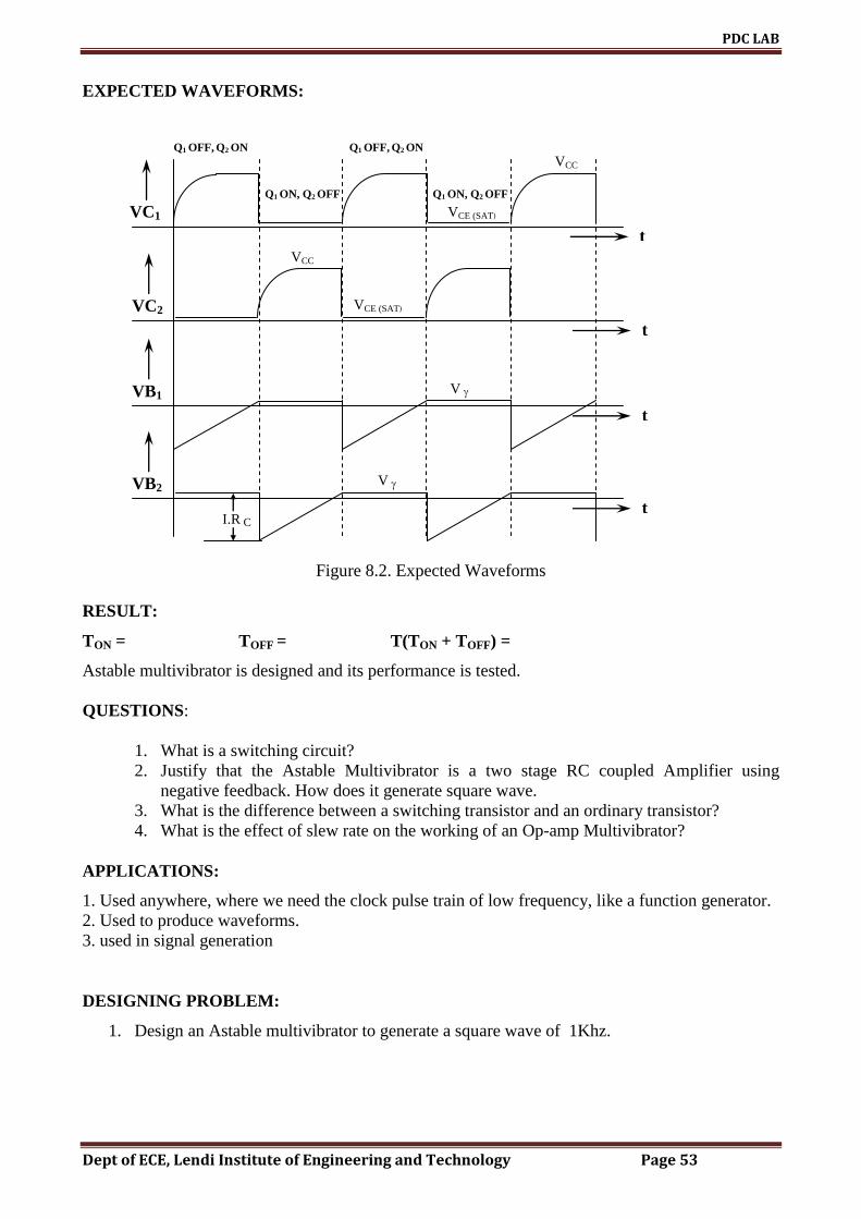
EXPECTED WAVEFORMS:
Q1 OFF, Q2 ON Q1 OFF, Q2 ON
Q1 ON, Q2 OFF Q1 ON, Q2 OFF
Figure 8.2. Expected Waveforms
RESULT:
TON = TOFF = T(TON + TOFF) =
Astable multivibrator is designed and its performance is tested.
QUESTIONS:
1. What is a switching circuit?
2. Justify that the Astable Multivibrator is a two stage RC coupled Amplifier using
negative feedback. How does it generate square wave.
3. What is the difference between a switching transistor and an ordinary transistor?
4. What is the effect of slew rate on the working of an Op-amp Multivibrator?
APPLICATIONS:
1. Used anywhere, where we need the clock pulse train of low frequency, like a function generator.
2. Used to produce waveforms.
3. used in signal generation
DESIGNING PROBLEM:
1. Design an Astable multivibrator to generate a square wave of 1Khz.
VC1
t
VC2
t
VB1
t
VB2
t
VCE (SAT)
VCE (SAT)
VCC
V
V
VCC
I.RC

PDC LAB
Dept of ECE, Lendi Institute of Engineering and Technology Page 54

PDC LAB
Dept of ECE, Lendi Institute of Engineering and Technology Page 55
GRAPH

PDC LAB
Dept of ECE, Lendi Institute of Engineering and Technology Page 56
EXPERIMENT NO: 9 Date:
MONOSTABLE MULTIVIBRATOR
AIM : To design and test performance of a monostable multivibrator to generate clock
pulse for a given frequency. And obtain the waveforms.
COMPONENTS REQUIRED:
1. Resistors 2.2KΩ-2
10KΩ-1
1KΩ-2
1.5 KΩ-1
2. Capacitors- 0.1µF
1 µF
3. Transistors 2N2369 – 2
4. Diode QA79-1
APPARATUS REQUIRED:
1. CRO
2. Power supply 0-30V
3. Bread board
4. Connecting wires
CIRCUIT DIAGRAM:
Figure 9.1. Monostable multivibrator
THEORY :
„A monostable multivibrator has only one stable state, the other state being quasi-
stable. Normally the multivibrator is in the stable state, and when an external triggering pulse is
applied, it switches from the stable to the quasi-stable state. It remains in the quasi-stable state fro a

PDC LAB
Dept of ECE, Lendi Institute of Engineering and Technology Page 57
short duration, but automatically reverts i.e. switches back to its original stable state, without any
triggering pulse‟.
Principle of operation
A collector-coupled Monostable multivibrator of the two transistors Q1 and Q2, Q1 is
normally OFF and Q2 is Normally ON. Resistor R1 and R2 are connected to the normally OFF
transistor, and the capacitor C is connected to the normally ON transistor.
It is seen from the circuit of the monostable multivibrator that, under normal conditions, the
supply voltage VCC provides enough base drive to the transistor Q2 through resistor R, with the
result that Q2 goes into saturation. With Q2 ON, Q1 goes OFF, as already studied in the context of
binary operation.
With Q2 ON and Q1 OFF, the capacitor finds a charging path. The voltage across the
capacitor is VCC with polarity. It is obvious that in the stable state of the multivibrator, Q2 is ON
and Q1 is OFF.
If the negative triggering pulse is applied to the collector of Q1, it is transmitted to the base
of Q2 through the capacitor, and hence makes the base of Q2 negative. Immediately Q2 goes OFF
and Q1 becomes ON. However, this is only a quasi-stable state as is obvious form the following
observation.
With Q1 ON and Q2 OFF, the capacitor C finds a discharging path. As the capacitor
discharges, it is seen that the potential at the base of the transistor Q2 becomes less and less
negative, and after a time, we have VB = V, the cut-in-voltage of Q2.
As soon as VB crosses the level of V, Q2 starts conducting and gets saturated. When
Q2 becomes ON, Q1 becomes OFF. Thus the original stable state of the multivibrator is restored.
[ In quasi-stable state: Q1 is ON and Q2 is OFF]
The interval during which the quasi-stable state of the multivibrator persists i.e., Q2 remains
OFF is dependent upon the rate at which the capacitor C discharges. This duration of the quasi-
stable state is termed as delay time or pulse width or gate time. It is denoted as T. The wave forms
of the voltage at base of the transistor Q2 and C (Collector of Q1)
DESIGN:
VCE = 5.56v, VCC = 6v, VCE(sat) = 0.3v, VBE(sat), = 0.7v, IC = 6mA,VF = -0.3v
Rc = (VCC–VCE(sat))/IC.
C
CsatBE
C
CCCE
RR
RV
RR
RVV
1
)(
1
1
Find the values of R1 and R2
PROCEDURE:
1. Connect the circuit as shown in figure.
2. With the help of a triggering circuit and using the condition T (trig) >
T(Quasi) a pulse waveform is generated.
3. The output of the triggering circuit is connected to the base of the off
transistor.
4. The Off transistor goes into ON state.
5. Observe the waveforms at VBE1, VBE2, VCE1, VCE2
6. Keep the DC- AC control of the Oscilloscope in DC mode.
EXPECTED WAVEFORMS:
21
2)(
21
1
RR
RV
RR
RVV
satCEBBF

PDC LAB
Dept of ECE, Lendi Institute of Engineering and Technology Page 58
Q2 OFF, Q1 ON Q1 OFF, Q2 ON
Q2 ON, Q1 OFF
Figure 9.2. Expected Waveforms
RESULT:
TON =
TOFF =
Total T (TON + TOFF) =
Monostable multivibrator is designed and studied.
QUESTIONS:
1. Explain the operation of collector coupled Monostable Multivibrator?
2. Derive the expression for the gate width of a transistor Monostable Multivibrator?
3. Give the application of a Monostable Multivibrator.
APPLICATIONS:
1. Frequency divider
2. Pulse width modulation
3. Linear ramp generator
4. Missing pulse detector
DESIGNING PROBLEM:
1. Design a collector coupled one shot with a gate width of 3ms, using n-p-n
transistors.
VC2
t
VB2 t
VC1
t
VB1
t
VCE (SAT)
VCE (SAT)
VCC
V
V
VCC
I.RC

PDC LAB
Dept of ECE, Lendi Institute of Engineering and Technology Page 59

PDC LAB
Dept of ECE, Lendi Institute of Engineering and Technology Page 60
GRAPH
PDC LAB
Dept of ECE, Lendi Institute of Engineering and Technology Page 61
EXPERIMENT NO: 10 Date:
SCHMITT TRIGGER
AIM: To design and analyze Schmitt trigger and to observe the waveforms.
COMPONENTS REQUIRED:
1. Resistors 100 KΩ-1
2.2 KΩ-2
3.3 KΩ-1
3.9 KΩ-1
6.8 K Ω-1
2. Capacitors 0.01µF-1
2. Transistors BC 107 – 2
APPARATUS:
1. Bread board
2. Power supply 0-30V
3. Signal generator
4. CRO
5. Connecting Wires.
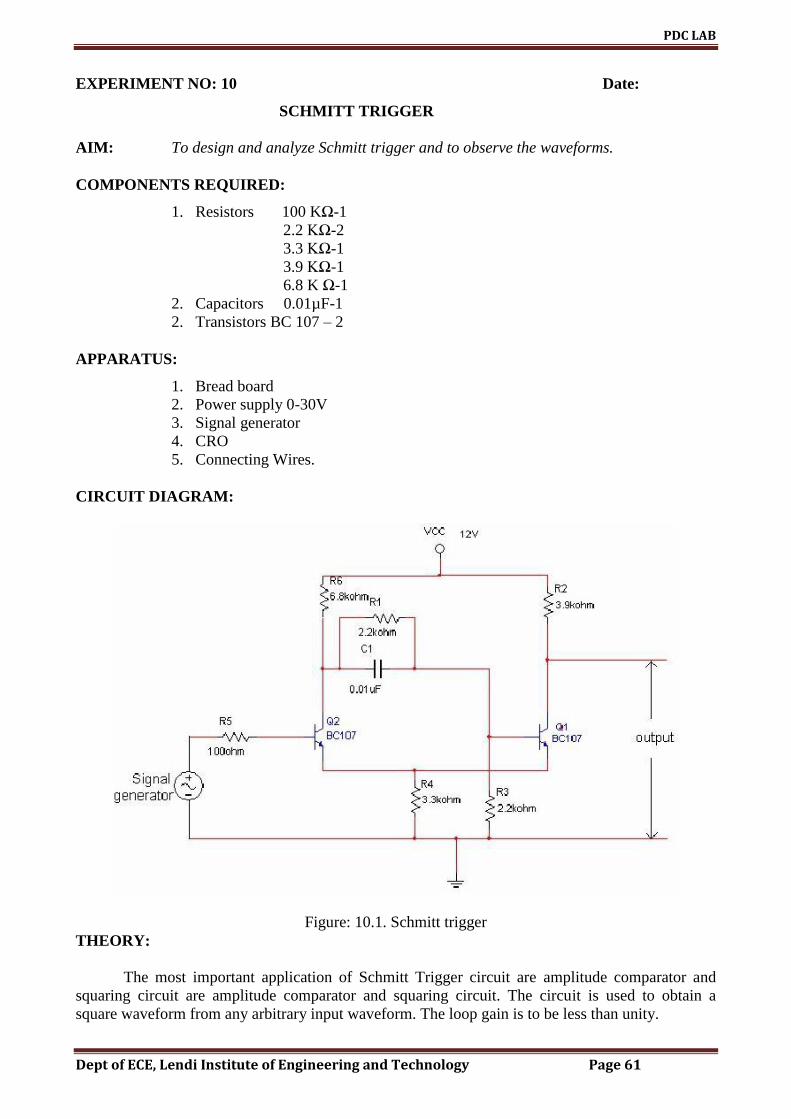
CIRCUIT DIAGRAM:
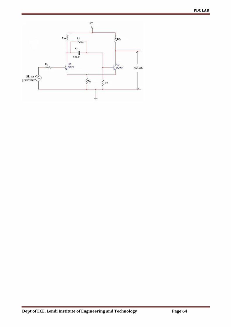
Figure: 10.1. Schmitt trigger
THEORY:
The most important application of Schmitt Trigger circuit are amplitude comparator and
squaring circuit are amplitude comparator and squaring circuit. The circuit is used to obtain a
square waveform from any arbitrary input waveform. The loop gain is to be less than unity.

PDC LAB
Dept of ECE, Lendi Institute of Engineering and Technology Page 62
If Q2 is conducting there will be voltage drop across RZ which will elevate the emitter of Q1.
Consequently if V is small enough in voltage, Q1 will be cut-off with Q1 conducting, the circuit
amplifies and since the gain is positive, the output to rise, V2 continues to fall and Z2 continues to
rise. Therefore a value of V will be reached where Q2 is turned OFF. At the point the output no
longer responds to the input.
Here the input signal is arbitrary except that it has large enough excursion to carry input
beyond the limits of hysteresis range, VH = (V1 – V2).
The output is a square wave whose amplitude is independent of the amplitude of the input
waveform.
DESIGN:
IC2 = 5mA
(Rc2 + RE) = VCC / IC2
U.T.P = VE2 = 5V
VE2 = (RE VCC) / (Rc2+RE)
I2 = 0.1IC2
L.T.P = VE1 = 3V
R2 = ER2i / I2 = VE1 / I2 = L.T.P / I2
Rc1 = (REVCC) / VE1 –RE
IB2 = IC2 / hfe(min)
(VCC - VE2) / (R1+RL1))) = (VE2/R2)+IB2
RB = (hfeRE) / 10
Find R1, R2, RE, Rc1and Rc2 from the above equations
PROCEDURE:
1. Connect the circuit as shown in figure 1 with designed values.
2. Apply VCC of 12V and an input frequency of 1KHz with an amplitude more than the
designed UTP.
3. Now note down the output wave forms
4. Observe that the output comes to ON state when input exceeds UTP and it comes to OFF
state when input comes below LTP
5. Observe the waveforms at VC1, VC2, VB2 and VE and plot graphs.
6. Keep the DC- AC control of the Oscilloscope in DC mode.
PDC LAB
Dept of ECE, Lendi Institute of Engineering and Technology Page 63
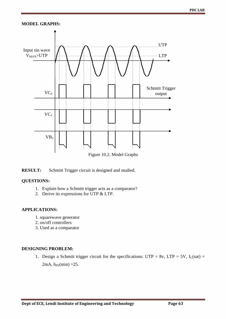
MODEL GRAPHS:
Figure 10.2. Model Graphs
RESULT: Schmitt Trigger circuit is designed and studied.
QUESTIONS:
1. Explain how a Schmitt trigger acts as a comparator?
2. Derive its expressions for UTP & LTP.
APPLICATIONS:
1. squarewave generator
2. on/off controllers
3. Used as a comparator
DESIGNING PROBLEM:
1. Design a Schmitt trigger circuit for the specifications: UTP = 8v, LTP = 5V, IC(sat) =
2mA, hFE(min) =25.
VC2
VC1
VB2
Input sin wave
VMAX>UTP
UTP
LTP
Schmitt Trigger
output
PDC LAB
Dept of ECE, Lendi Institute of Engineering and Technology Page 64

PDC LAB
Dept of ECE, Lendi Institute of Engineering and Technology Page 65
GRAPH

PDC LAB
Dept of ECE, Lendi Institute of Engineering and Technology Page 66
EXPERIMENT NO: 11 Date:
UJT RELAXATION OSCILLATOR
AIM : To obtain a saw tooth waveform using UJT and test its performance as an oscillator
and also obtain the error.
COMPONENTS:
1. Resistors 47k-1
100-1
2. Capacitor 0.1F-1
3. UJT 2n2646-1
APPARATUS
1. Bread board
2. Power supply 0-30V
3. CRO
THOERY :
A Unijunction transistor (UJT), as the very implies, has only one p-n junction, unlike a BJT
which has two p-n junctions’.
11.1. Equivalent Circuit of UJT Relaxation Oscillator
The equivalent circuit of the UJT is as shown in figure 1.
RB1 is the resistance between base B1 and the emitter, and it is basically a variable resistance,
its value being dependent upon the emitter current IE.
RB2 is the resistance between base B2 and the emitter, and the value is fixed. Consider the circuit as shown in figure 1.
Let IE = 0. Due to the applied voltage VBB a current I results as shown.
We have V1 = iRB1.

PDC LAB
Dept of ECE, Lendi Institute of Engineering and Technology Page 67
VP = V + VBB
0,when
21
1E
BB
B IRR
R
But 21 BB
BB
RR
Vi
1
21
1 B
BB
BB RRR
VV
BB
BB
B VRR
R
21
1
The ratio
21
1
BB
B
RR
Ris termed as the intrinsic stand
off ratio and it is denoted as .
Figure 11.2
BBVV 1 .
Form the equivalent circuit, it is evident that the diode cannot conduct unless the emitter voltage VE
= V + V1, where V is the cutin voltage of the diode.
This value of the emitter voltage which makes the diode conduct is termed as peak voltage,
and it is denoted as VP.
We have VE = V + V1,
V1 = VBB. or since
It is obvious that if VE < VP, the UJT is OFF, and
if VE < VP, the UJT is ON.
Figure 11.3. Shows the emitter characteristics of a UJT (plot of VE vs IE)
Figure 11.3. Emitter characteristics of a UJT
The main application of UJT is in switching circuits wherein rapid discharging of capacitor
is very essential.
Having understood the basic of UJT, we shall next study the working of UJT relaxation
oscillator.
RB2
RB1
VBB
V1
i
0 IP IV IE
VV
VP
VE
Peak Point
Valley Point
Negative
resistance
region

PDC LAB
Dept of ECE, Lendi Institute of Engineering and Technology Page 68
RB2
RB1
R
C Vs
+
-
V or VBB
B2
B1
E
Working of UJT relaxation oscillator (OR UJT sweep circuit)
Figure:11.4. UJT relaxation oscillator
The UJT sweep circuit shown in the figure 4 consists of a UJT, a capacitor and a resistor
arranged as shown.
We studied that a UJT is OFF as long as VE < VP, the peak voltage. Hence initially when the
UJT is OFF, the capacitor C charges through the resistance R from the supply voltage V.
Let VS = capacitor voltage.
It is seen that when the capacitor voltage VS rises to the value VP the UJT readily conducts.
When the UJT becomes ON, the capacitor discharges and its voltage falls. When the voltage falls to
the valley point VV, the UJT becomes OFF and the capacitor charges again to VP.
This cycle of charging and discharging of the capacitor C repeats, and as a result, a saw
tooth wave form of voltage across C is generated.
CIRCUIT DIAGRAM :
1. Emitter 2. Base1 3. Base2
Figure:11.5. Circuit Diagram of UJT relaxation oscillator
PROCEDURE:
1. Connect the circuit as shown in figure with designed values.
2. Note down the voltages and frequencies across C& R2 .
3. The time period of the output wave form is noted and is compared with theoretical value
T = R1 C[ ln (VBB – VV) / (VBB – VP)]
VCC =12V R
1
C
B
2 B
1
E 47k
0.1
F
R
2 100
2N26
46

PDC LAB
Dept of ECE, Lendi Institute of Engineering and Technology Page 69
4. Plot the graphs of Vc and VR1.
EXPECTED WAVEFORMS:
VC VR2
VP
VV
t t
RESULT:
Theoretical T = Practical T =
Sawtooth waveform is obtained using UJT and its performance as an oscillator is studied.
QUESTIONS:
1. Describe some important applications of a UJT?
2. Is the name UJT appropriate?
3. Write short notes on UJT as a relaxation oscillator?
4. Discuss the concept of –ve resistance?
5. Define the intrinsic stand off ratio and explain its importance?
APPLICATIONS:
1. Sawtooth wave generator
2. Used in Phase Shifters.
DESIGNING ROBLEM:
1. The specifications of UJT are given as η = 0.6, Vv = 2V, RBB = 5KΩ,Iv = 1.5mA, Ip = 8µA
and VBB = 18V. Calculate the component values of the UJT sweep circuit to generate an
output sweep frequency of 10KHZ with swee amplitude of 12V.

PDC LAB
Dept of ECE, Lendi Institute of Engineering and Technology Page 70
GRAPH
PDC LAB
Dept of ECE, Lendi Institute of Engineering and Technology Page 71
10µF
VCC = 12V
-VBB =-10V
100µF
0.1µF
100K 5.6K
10K
IN4007
2N2369
V0 Vi 2N2369
Q1
Q2
EXPERIMENT NO: 12 Date:
BOOT STRAP SWEEP CIRCUIT
AIM: To design and test the performance of bootstrap sweep circuit.
COMPONENTS REQUIRED:
1. Resistors 100K-1
5.6K-1
10K-1
2.Capacitors 0.1F-1,
10F-1
100F-1
3. Diode IN4007-1
4. Transistors 2N2369– 2
APPARATUS REQUIRED:
1. Bread board
2. Power supply
3. CRO
4. Signal generator
5. Connecting Wires.
CIRCUIT DIAGRAM:
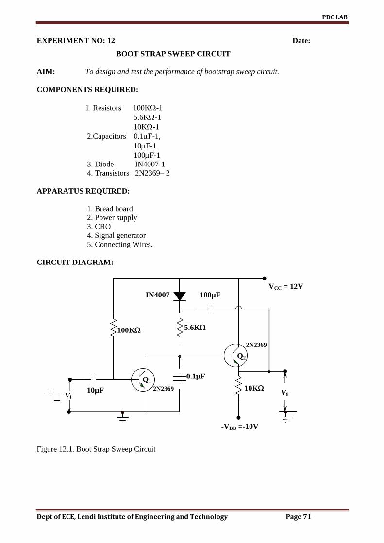
Figure 12.1. Boot Strap Sweep Circuit
PDC LAB
Dept of ECE, Lendi Institute of Engineering and Technology Page 72
DESIGN:
RC
TVV
gCC
S
)/1()/(
/)(
RRh
VVCT
Bfe
CCSR
Sweep time = TS = RC
THEORY:
The input to Q1 is the gating waveform. Before the application of the gating waveform, at t
= 0, transistor Q1 is in saturation. The voltage across the capacitor C and at the base of Q2 is VCE(sat).
To ensure Q1 to be in saturation for t = 0, it is necessary that its current be at least equal to iCE / hFE
so that Rb < hfeR.
With the application of the gating waveform at t = 0, Q1 is driven OFF. The current iC1 now
flow into C and assuming units gain in the emitter followerRC
tVV CC0 . When the sweep starts, the
diode is reverse biased, as already explained above, the current through R is supplied by C1. The
current VCC / R through C and R now flows from base to emitter of Q2.if the output V0 reaches the
voltage VCC in a time TS / Tg, then from above we have TS = RC.
If the sweep amplitude is less than VCC, then the maximum ramp voltage is given by
RC
TVV
gCC
S
PROCEDURE:
1. Connect the circuit as shown in figure.
2. Apply the square wave or rectangular wave form at the input terminals.
3. Connect the CRO at output terminals now plug the power card into line switch on and observe
the power indication.
4. As mentioned in circuit practical calculation. Observe and record the output waveforms from
CRO and compare with theoretical values.
PDC LAB
Dept of ECE, Lendi Institute of Engineering and Technology Page 73
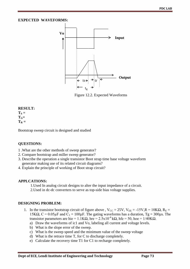
EXPECTED WAVEFORMS:
Vo
Input
Output
Figure 12.2. Expected Waveforms
RESULT:
TS =
TG=
TR =
Bootstrap sweep circuit is designed and studied
QUESTIONS:
1 .What are the other methods of sweep generator?
2. Compare bootstrap and miller sweep generator?
3. Describe the operation a single transistor Boot strap time base voltage waveform
generator making use of its related circuit diagrams?
4. Explain the principle of working of Boot strap circuit?
APPLCATIONS:
1.Used In analog circuit designs to alter the input impedance of a circuit.
2.Used in dc-dc converters to serve as top-side bias voltage supplies.
DESIGNING PROBLEM:
1. In the transistor bootstrap circuit of figure above , VCC = 25V, VEE = -15V,R = 10KΩ, RE =
15KΩ, C = 0.05µF and C1 = 100µF. The gating waveforms has a duration, Tg = 300µs. The
transistor parameters are hie = 1.1KΩ, hre = 2.5x10⁻⁴
kΩ, hfe = 50, hoe = 1/40KΩ.
a) Draw the waveforms of ic1 and Vo, labeling all current and voltage levels.
b) What is the slope error of the sweep.
c) What is the sweep speed and the minimum value of the sweep voltage
d) What is the retrace time T, for C to discharge completely.
e) Calculate the recovery time T1 for C1 to recharge completely.
ts
tg
tr

PDC LAB
Dept of ECE, Lendi Institute of Engineering and Technology Page 74

PDC LAB
Dept of ECE, Lendi Institute of Engineering and Technology Page 75
GRAPH
PDC LAB
Dept of ECE, Lendi Institute of Engineering and Technology Page 76
EXPERIMENT NO: 13 Date:
SAMPLING GATES
AIM: To construct and verify the response of sampling gate by using diode.
COMPONENTS:
1. Resistors (1 kΩ, 10 kΩ)
2. Capacitor (0.047µf)
3. Diode 1N4007
APPARATUS:
1. Function generator
2. CRO
3. Connecting wires
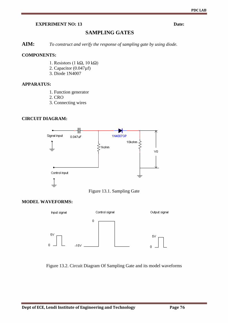
CIRCUIT DIAGRAM:
Figure 13.1. Sampling Gate
MODEL WAVEFORMS:
Figure 13.2. Circuit Diagram Of Sampling Gate and its model waveforms

PDC LAB
Dept of ECE, Lendi Institute of Engineering and Technology Page 77
THEORY:
An ideal sampling gate is a transmission circuit that produces an output signal
identical to the input signal during a selected time interval.the output of the sampling gate is zero
outside this selected time interval.the sampling gate is open during the sampling interval and it is
closed at all other times.the time interval for transmission is monitored by a control input
signal,which is usually rectangular in shape.in practice the idealized transmission gate is not
realized.as long as the output is produced at the correct time the performance of the practical
sampling gates available is treated to be quite satisfactory.
PROCEDURE:
1. Connect the circuit as per circuit diagram
2. Apply both inputs (signal input and control input) simultaneously to the
circuit.
3. Repeat the second step by varying input signal and putting control signal
fixed.
4. Note down the output waveforms for various range of input signals.
PRECAUTIONS:
1. Connections should be tight.
2. Take care when applying the control signal.
RESULT: Hence verified the response of sampling gate by using diode.
QUESTIONS:
1. What is sampling gate?
2. Define control signal?
3. What is the other name for the control signal?
4. What is the difference between logic gates and sampling gates?
5. What is the necessity of the sampling gate?
APPLICATIONS:
Used in
1. Multiplexers
2. D/A converters
3. Chopper stabilized amplifiers
4. Sampling scopes.
5. Sampling and hold circuits.

PDC LAB
Dept of ECE, Lendi Institute of Engineering and Technology Page 78
GRAPH

PDC LAB
Dept of ECE, Lendi Institute of Engineering and Technology Page 79
PROJECTS
MOSQUITO CONTROL CIRCUIT:
circuit daigram
Components required
1. Power supply (12V)
2. Resistors (2.7kΩ x 2)
3. Capacitors (0.01µF x 2)
4. NE 555 timer
5. IC Diode (1N4007)
6. Piezo Buzzer
Working of bug repellent circuit
Here the 555 timer is configured in astable multivibrator mode, specifically devised for generating
sound at the ultra frequency levels.The frequency of this circuit is set to 25 kHz, this frequency falls
in the ultrasound region and it is not audible to human beings. The 1N4007 diode is used to get 50%
duty cycle for the frequency generator.The piezo buzzer converts the output of 555 astable to

PDC LAB
Dept of ECE, Lendi Institute of Engineering and Technology Page 80
ultrasonic sound that can be heard by the insects.This ultrasound frequency cause some irritations
and uneasiness to the insects such as mosquitoes. However it will not disturb you if you have
installed this circuit of insect repellent for your home.
DANCING LIGHT
circuit daigram
Cponents required
As indicated in the circuit diagram
Working principal
Here is a simple dancing light circuit Based on NE555(IC1) & CD4017(IC2). The IC1 is
wored as an astable multivibrator to provide the clock pulses for the CD4017.for each clock pulse
receiving at the clock input (pin14) of IC CD4017,the outputs Q0 to Q9 becomes high one by one
alternatively.the leds connected to these pins glow in the same fashion to give a Dancing effect.the
speed of the dancing LEDs depend on the frequency of the clock pulses generated by the IC1.

PDC LAB
Dept of ECE, Lendi Institute of Engineering and Technology Page 81
CLAP SWITCH
Circuit diagram
Components required
Resistors
R1=15KΩ, R5,R6=1.5KΩ
R2,R11,R12=2.2MΩ, R13=2.2KΩ
R3=270KΩ, R4=3.3KΩ
R7,R8=10KΩ, R9,R10=27KΩ
Capacitors
C1=1000µf/16v
C2=.01µf,C3,C4=.047µf
Semi Conductors
Q1,Q2,Q3= BC548
D2,D3,D4= IN 4148
D1,D5=IN 4007, Q4=BC368
Misc
T1=12v/500mA Transformer
Mic= Condenser Microphone
K1= 12V Relay, B1= Bulb or Load
PDC LAB
Dept of ECE, Lendi Institute of Engineering and Technology Page 82
Working principle
Here is a Hobby Circuit for electronics hobbyists that can switch on & off a light, Fan, Radio
etc., by the sound of clap. The sound of clap is received by a small microphone that is shown biased by
resistor R1 in the circuit. The microphone changes sound wave in to electrical wave, which is further
amplified by Q1. Transistor Q1 is used as common emitter circuit to amplify weak signals received by
the microphone. Amplified output from the collector of transistor Q1 is feed to the Bistable
Multivibrator circuit also known as flip-flop circuit.
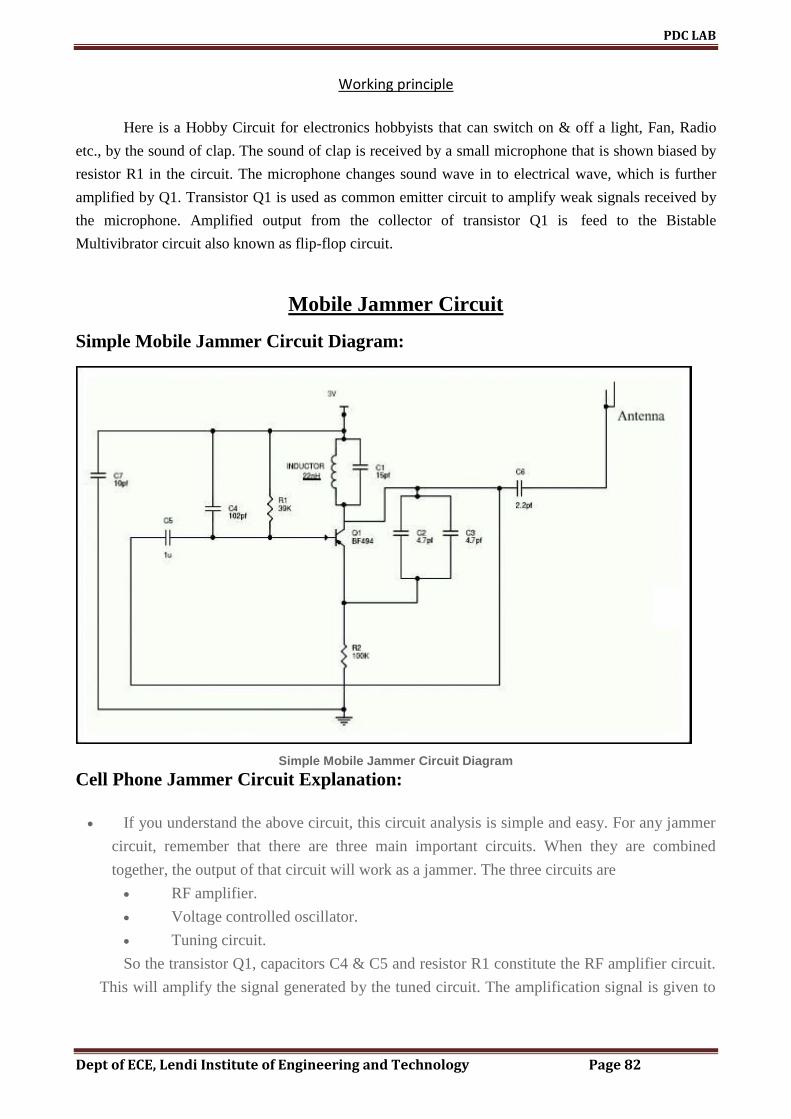
Mobile Jammer Circuit
Simple Mobile Jammer Circuit Diagram:
Simple Mobile Jammer Circuit Diagram
Cell Phone Jammer Circuit Explanation:
If you understand the above circuit, this circuit analysis is simple and easy. For any jammer
circuit, remember that there are three main important circuits. When they are combined
together, the output of that circuit will work as a jammer. The three circuits are
RF amplifier.
Voltage controlled oscillator.
Tuning circuit.
So the transistor Q1, capacitors C4 & C5 and resistor R1 constitute the RF amplifier circuit.
This will amplify the signal generated by the tuned circuit. The amplification signal is given to
PDC LAB
Dept of ECE, Lendi Institute of Engineering and Technology Page 83
the antenna through C6 capacitor. Capacitor C6 will remove the DC and allow only the AC
signal which is transmitted in the air.
When the transistor Q1 is turned ON, the tuned circuit at the collector will get turned ON.
The tuned circuit consists of capacitor C1 and inductor L1. This tuned circuit will act as an
oscillator with zero resistance.
This oscillator or tuned circuit will produce the very high frequency with minimum
damping. The both inductor and capacitor of tuned circuit will oscillate at its resonating
frequency.
The tuned circuit operation is very simple and easy to understand. When the circuit gets ON,
the voltage is stored by the capacitor according to its capacity. The main function of capacitor is
to store electric energy. Once the capacitor is completely charged, it will allow the charge to
flow through inductor. We know that inductor is used to store magnetic energy. When the
current is flowing across the inductor, it will store the magnetic energy by this voltage across
the capacitor and will get decreased, at some point complete magnetic energy is stored by
inductor and the charge or voltage across the capacitor will be zero. The magnetic charge
through the inductor will decreased and the current will charge the capacitor in opposite or
reverse polarity manner. Again after some period of time, capacitor will get completely charged
and magnetic energy across the inductor will be completely zero. Again the capacitor will give
charge to the inductor and becomes zero. After some time, inductor will give charge to capacitor
and become zero and they will oscillate and generate the frequency.
This circle run upto the internal resistance is generated and oscillations will get stop. RF
amplifier feed is given through the capacitor C5 to the collector terminal before C6 for gain or
like a boost signal to the tuned circuit signal. The capacitors C2 and C3 are used for generating
the noise for the frequency generated by the tuned circuit. Capacitors C2 and C3 will generate
the electronic pulses in some random fashion (technically called noise).
The feedback back or boost given by the RF amplifier, frequency generated by the tuned
circuit, the noise signal generated by the capacitors C2 and C3 will be combined, amplified and
transmitted to the air.
Cell phone works at the frequency of 450 MHz frequency. To block this 450MHz
frequency, we also need to generate 450Mhz frequency with some noise which will act as
simple blocking signal, because cell phone receiver will not be able to understand to which
signal it has been received. By this, we can able to block the cell phone signal from reaching the
cell phones.
So here in the above circuit, we generated the 450 MHz frequency to block the actual cell
phone signal. That‟s what the above circuit will act as a jammer for blocking the actual signal.
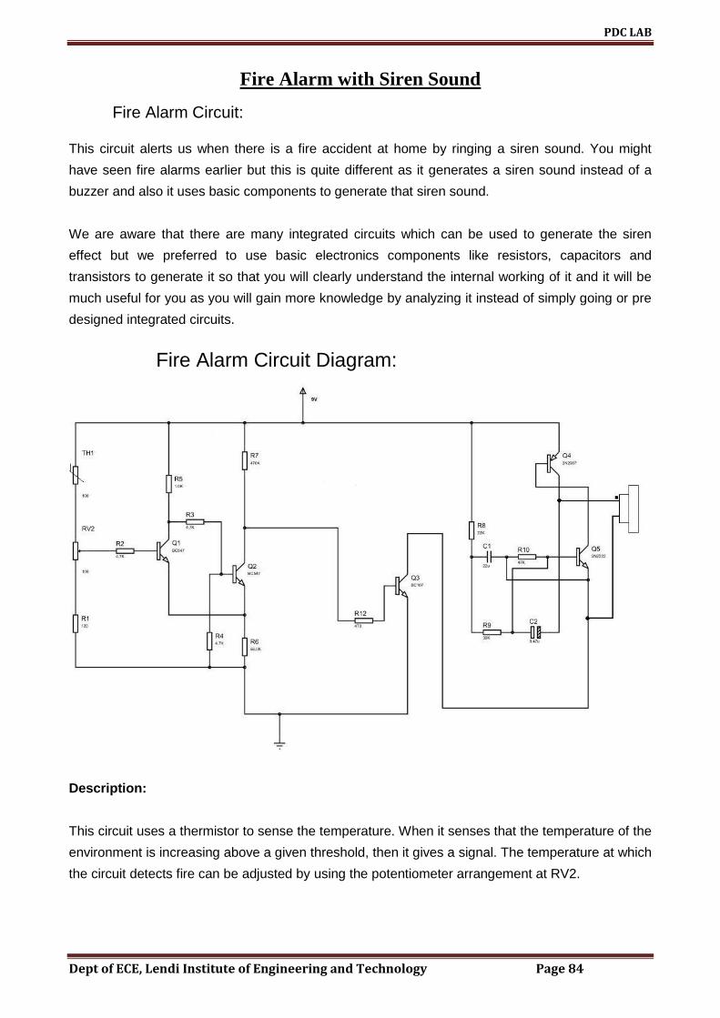
PDC LAB
Dept of ECE, Lendi Institute of Engineering and Technology Page 84
Fire Alarm with Siren Sound
Fire Alarm Circuit:
This circuit alerts us when there is a fire accident at home by ringing a siren sound. You might
have seen fire alarms earlier but this is quite different as it generates a siren sound instead of a
buzzer and also it uses basic components to generate that siren sound.
We are aware that there are many integrated circuits which can be used to generate the siren
effect but we preferred to use basic electronics components like resistors, capacitors and
transistors to generate it so that you will clearly understand the internal working of it and it will be
much useful for you as you will gain more knowledge by analyzing it instead of simply going or pre
designed integrated circuits.
Fire Alarm Circuit Diagram:
Description:
This circuit uses a thermistor to sense the temperature. When it senses that the temperature of the
environment is increasing above a given threshold, then it gives a signal. The temperature at which
the circuit detects fire can be adjusted by using the potentiometer arrangement at RV2.

PDC LAB
Dept of ECE, Lendi Institute of Engineering and Technology Page 85
When the temperature increases above the set value, the potentiometer arrangement produces a
high voltage. This voltage is then given to BC547 transistor in common emitter mode. It is an NPN
general purpose transistor. When the base is given a high input, it gets turned on. When the
transistor is turned on, its collector voltage is reduced to low as the collector to emitter voltage
decreases. The collector output voltage of the first transistor is given to the base as an input to the
second BC 547 NPN transistor. This transistor too is in common emitter mode and as the input is
low when the temperature threshold is reached, the output at the collector will rise high. In this
state, it will turn on the next transistor, i.e BC107. This transistor will now act as a switch for the
siren circuit. This transistor can bear power quite larger than the BC547 and it is also equipped
with a heat sink for that purpose.
When the BC107 transistor turns on, it allows current to pass from power supply to ground through
collector thereby acting as an electronically controlled switch. When the current is passing, the
siren circuit which is assembled as the load to the circuit is turned ON. Then you can hear the siren
sound through the buzzer. The capacitors used in the circuit are the main components in
producing the siren effect. The principle involved in generating the siren effect is to make an
oscillator with an envelope which periodically increases and decreases so as to generate that
effect.
Battery Charger Circuit Using SCR
Introduction to Battery Charger Using SCR:
The battery is charged with small amount of AC voltage or DC voltage. So if you want to
charge your battery with AC source then should follow these steps, we need first limit the
large AC voltage, need to filter the AC voltage to remove the noise, regulate and get the
constant voltage and then give the resulting voltage to the battery for charging. Once
charging is completed the circuit should automatically turned off.
Block Diagram of Battery Charger Using SCR:
The AC source is given to the step down transformer which converts the large AC source
into limited AC source, filter the AC voltage and remove the noise and then give that
voltage to the SCR where it will rectify the AC and give the resulting voltage to the battery
for charging.
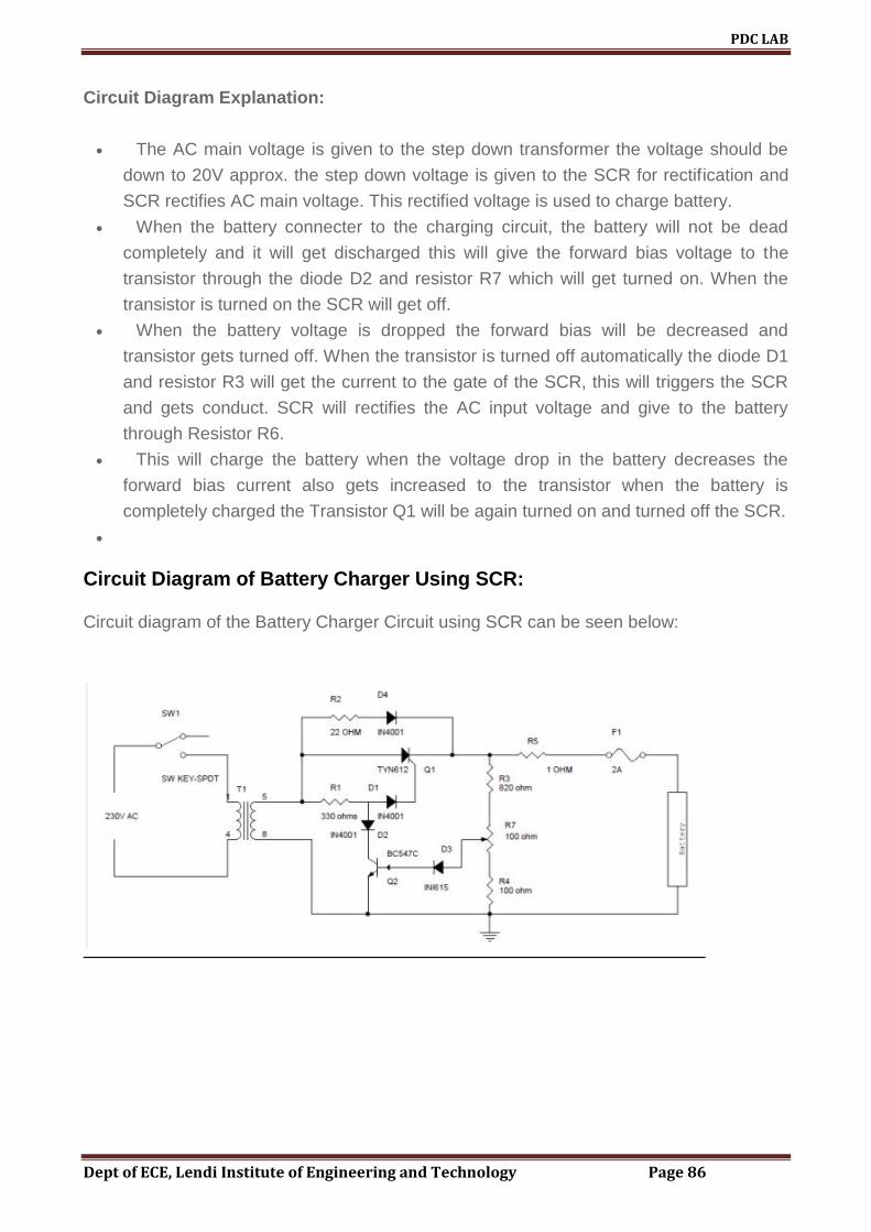
PDC LAB
Dept of ECE, Lendi Institute of Engineering and Technology Page 86
Circuit Diagram Explanation:
The AC main voltage is given to the step down transformer the voltage should be
down to 20V approx. the step down voltage is given to the SCR for rectification and
SCR rectifies AC main voltage. This rectified voltage is used to charge battery.
When the battery connecter to the charging circuit, the battery will not be dead
completely and it will get discharged this will give the forward bias voltage to the
transistor through the diode D2 and resistor R7 which will get turned on. When the
transistor is turned on the SCR will get off.
When the battery voltage is dropped the forward bias will be decreased and
transistor gets turned off. When the transistor is turned off automatically the diode D1
and resistor R3 will get the current to the gate of the SCR, this will triggers the SCR
and gets conduct. SCR will rectifies the AC input voltage and give to the battery
through Resistor R6.
This will charge the battery when the voltage drop in the battery decreases the
forward bias current also gets increased to the transistor when the battery is
completely charged the Transistor Q1 will be again turned on and turned off the SCR.
Circuit Diagram of Battery Charger Using SCR:
Circuit diagram of the Battery Charger Circuit using SCR can be seen below: