pumpkin's cubesat kit hinge - pumpkin, inc
TRANSCRIPT
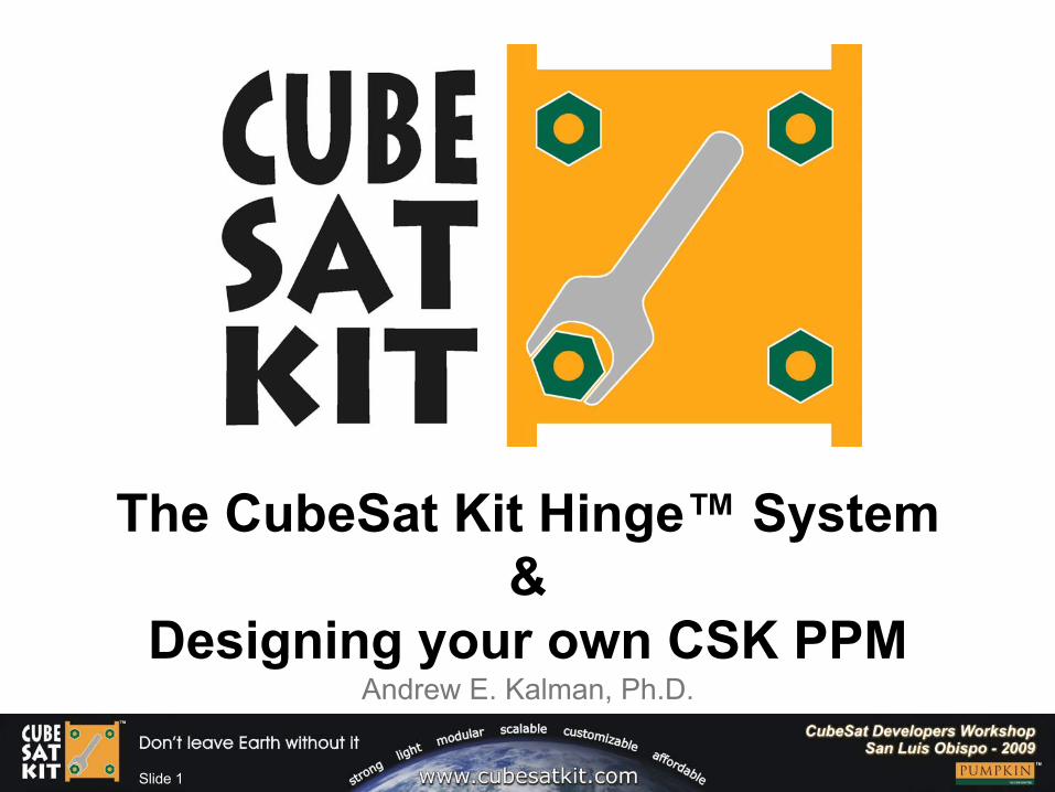
Slide 1
The CubeSat Kit Hinge™ System&
Designing your own CSK PPMAndrew E. Kalman, Ph.D.
Slide 2
Outline• Part I: The CubeSat Kit Hinge System• Part II: Design your own CubeSat Kit Pluggable
Processor Module (PPM)
Slide 3
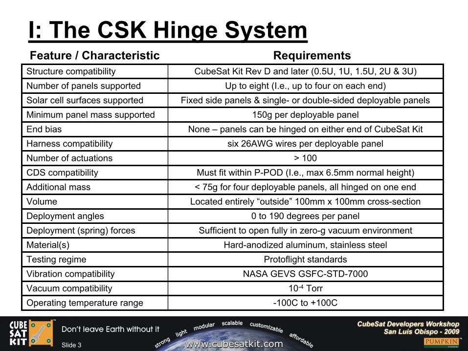
I: The CSK Hinge System
150g per deployable panelMinimum panel mass supported
> 100Number of actuations
None – panels can be hinged on either end of CubeSat KitEnd biassix 26AWG wires per deployable panelHarness compatibility
10-4 TorrVacuum compatibility
Sufficient to open fully in zero-g vacuum environmentDeployment (spring) forces
Must fit within P-POD (I.e., max 6.5mm normal height)CDS compatibility
Protoflight standardsTesting regime
Fixed side panels & single- or double-sided deployable panelsSolar cell surfaces supported
-100C to +100COperating temperature range
Up to eight (I.e., up to four on each end)Number of panels supported
Hard-anodized aluminum, stainless steelMaterial(s)
NASA GEVS GSFC-STD-7000Vibration compatibility
0 to 190 degrees per panelDeployment anglesLocated entirely “outside” 100mm x 100mm cross-sectionVolume< 75g for four deployable panels, all hinged on one endAdditional mass
CubeSat Kit Rev D and later (0.5U, 1U, 1.5U, 2U & 3U)Structure compatibilityRequirementsFeature / Characteristic

Slide 4
CSK Hinge Components• Hinge feet &
hinges• Precision shoulder
bolts• Springs• Large & small
buttons• Harnesses &
cables
Slide 5
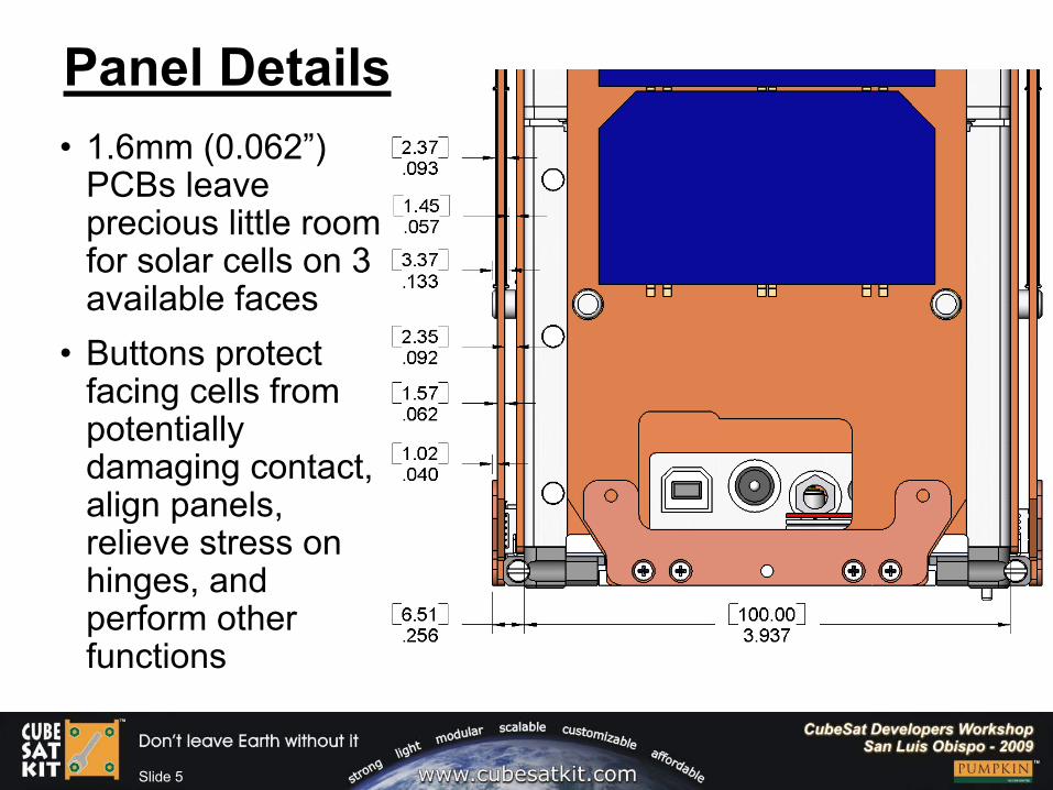
Panel Details• 1.6mm (0.062”)
PCBs leave precious little room for solar cells on 3 available faces
• Buttons protect facing cells from potentially damaging contact, align panels, relieve stress on hinges, and perform other functions
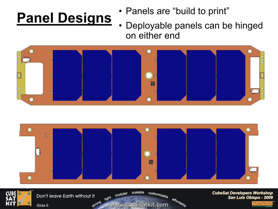
Slide 6
Panel Designs • Panels are “build to print”• Deployable panels can be hinged
on either end
Slide 7
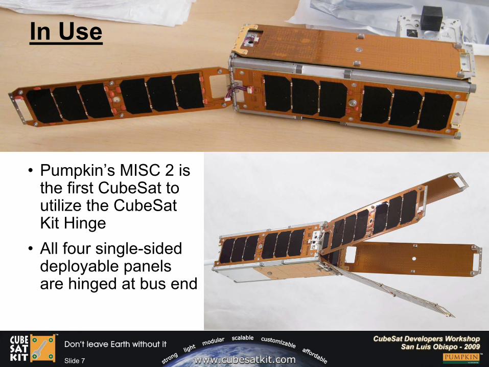
In Use
• Pumpkin’s MISC 2 is the first CubeSat to utilize the CubeSat Kit Hinge
• All four single-sided deployable panels are hinged at bus end
Slide 8
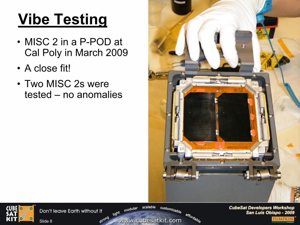
Vibe Testing• MISC 2 in a P-POD at
Cal Poly in March 2009• A close fit!• Two MISC 2s were
tested – no anomalies
Slide 9
II: Design your own CSK PPM• Pluggable Processor Modules (PPMs) enable rapid
adaptation of the CubeSat Kit architecture to an existing codebase that has tight ties to a particular processor architecture or family.
• The PPM:is where your CubeSat’s processor(s) is(are) locatedtakes power from the CSK bus, uses it locally, conditions it for the Motherboard (MB) and optionally for the CSK busaccepts a few high-level control signals from the CSK busconnects to various resources on the MBconnects to I/O and other signals on the CSK bus

Slide 10
CSK Architecture Block Diagram
Slide 11
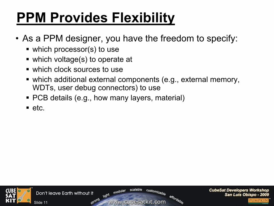
PPM Provides Flexibility• As a PPM designer, you have the freedom to specify:
which processor(s) to usewhich voltage(s) to operate atwhich clock sources to usewhich additional external components (e.g., external memory, WDTs, user debug connectors) to usePCB details (e.g., how many layers, material)etc.
Slide 12
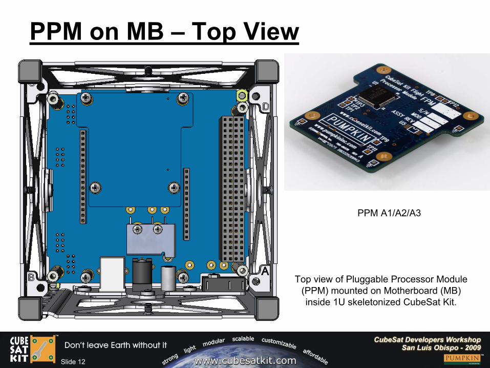
PPM on MB – Top View
Top view of Pluggable Processor Module (PPM) mounted on Motherboard (MB) inside 1U skeletonized CubeSat Kit.
PPM A1/A2/A3
Slide 13
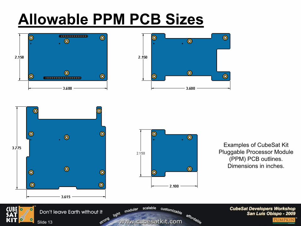
Allowable PPM PCB Sizes
Examples of CubeSat Kit Pluggable Processor Module
(PPM) PCB outlines. Dimensions in inches.
Slide 14
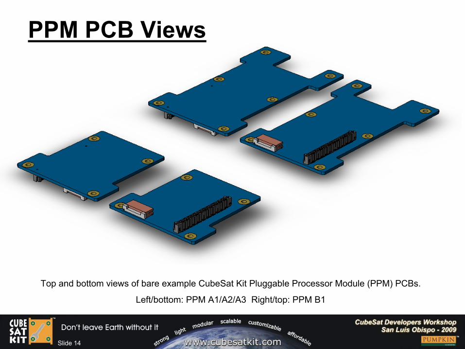
PPM PCB Views
Top and bottom views of bare example CubeSat Kit Pluggable Processor Module (PPM) PCBs.
Left/bottom: PPM A1/A2/A3 Right/top: PPM B1
Slide 15
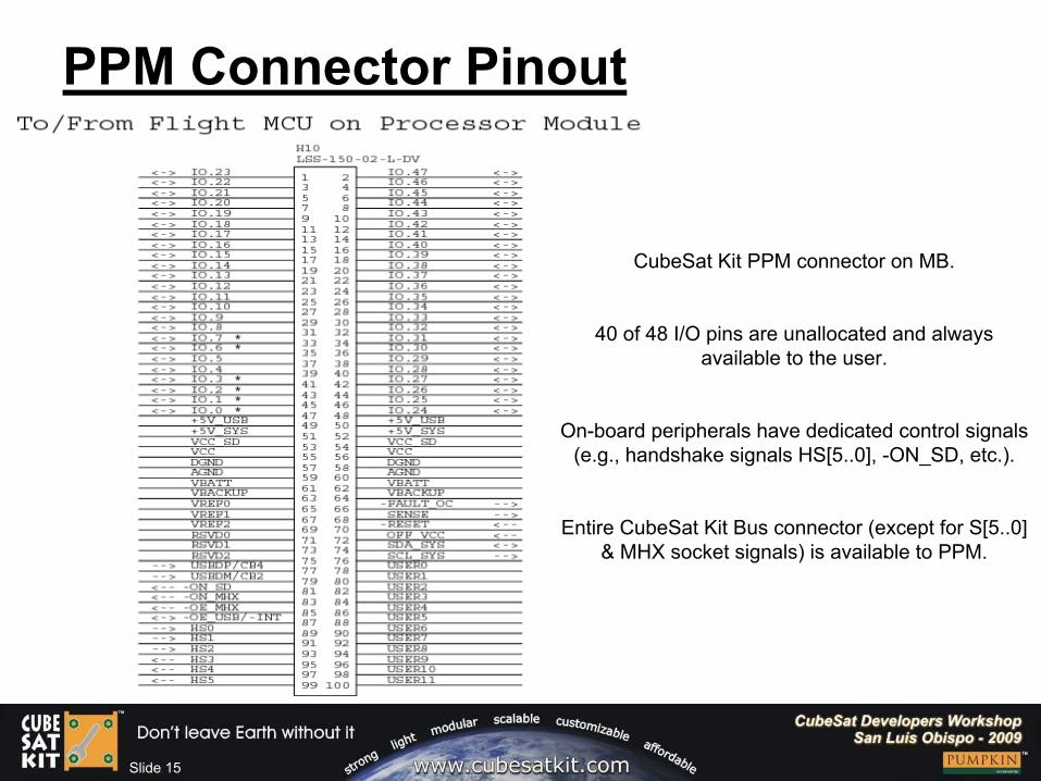
PPM Connector Pinout
CubeSat Kit PPM connector on MB.
40 of 48 I/O pins are unallocated and always available to the user.
On-board peripherals have dedicated control signals (e.g., handshake signals HS[5..0], -ON_SD, etc.).
Entire CubeSat Kit Bus connector (except for S[5..0] & MHX socket signals) is available to PPM.
Slide 16
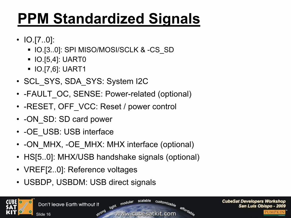
PPM Standardized Signals• IO.[7..0]:
IO.[3..0]: SPI MISO/MOSI/SCLK & -CS_SDIO.[5,4]: UART0IO.[7,6]: UART1
• SCL_SYS, SDA_SYS: System I2C• -FAULT_OC, SENSE: Power-related (optional)• -RESET, OFF_VCC: Reset / power control• -ON_SD: SD card power• -OE_USB: USB interface• -ON_MHX, -OE_MHX: MHX interface (optional)• HS[5..0]: MHX/USB handshake signals (optional)• VREF[2..0]: Reference voltages• USBDP, USBDM: USB direct signals
Slide 17
PPM User Signals & Power• PPM user signals
IO.[47..8] – as yet undefined, up to designer’s discretionUSER[11..0] – undefined
• PPM power +5V_USB & +5V_SYS: from EPS & USB to PPMVCC_SD: from PPM to MB SD Card, +3.3VVCC: on PPM, and to MB – can range from +2.7V to +5VDGND: Digital groundAGND: Analog (quiet) groundVBATT: Raw battery voltage (e.g. +7.4V)VBACKUP: +3V battery backup (e.g. for SRAM)
Slide 18
PPM A1: MSP430F1612• Utilizes TI’s MSP430F1612IPM (64-pin LQFP package)• Regulates +5V_SYS & +5V_USB down to +3.3V for processor, VCC
on MB and SD Card• Has local POR supervisor & overcurrent protection / auto-reset• Has 32.768kHz & 7.3728MHz crystals• All 48 I/O pins to IO.[47..0] on CSK bus• PCA9515 I2C isolator routes MSP430 SCL & SDA to SCL_SYS &
SDA_SYS, enabled via –CS_SD• Some I/O signals also routed to –ON_XX, -OE_XX, HS[5..0]• VREF[2..0] used• VBACKUP not used• 11g, small-footprint PCB
Slide 19
PPM B1: C8051F120• Utilizes SiLabs C8051F120-GQ (100-pin LQFP package)• Regulates +5V_SYS & +5V_USB down to +3.3V for processor, VCC on MB and
SD Card• Uses on-chip POR• Has local overcurrent protection / auto-reset• Has optional high-speed crystal• Has 1Mbit SRAM via P4.[7..5], P6.n, P7.n (multiplexed mode, paged)• Has 6-pin FPC user debug header• P0.n, P1.n, P2.n, P3.n, P4.0, AIN0.n, CP0/1 & DAC0/1 mapped to IO.[47..34,
30..0] on CSK bus• I2C (P0.[7,6]) direct to SCL_SYS & SDA_SYS• –ON_XX, -OE_XX, HS[5..0] on dedicated lines via P4 & P5• VREF[2..0] used• VBACKUP used for SRAM backup• 17g, medium-footprint PCB
Slide 20
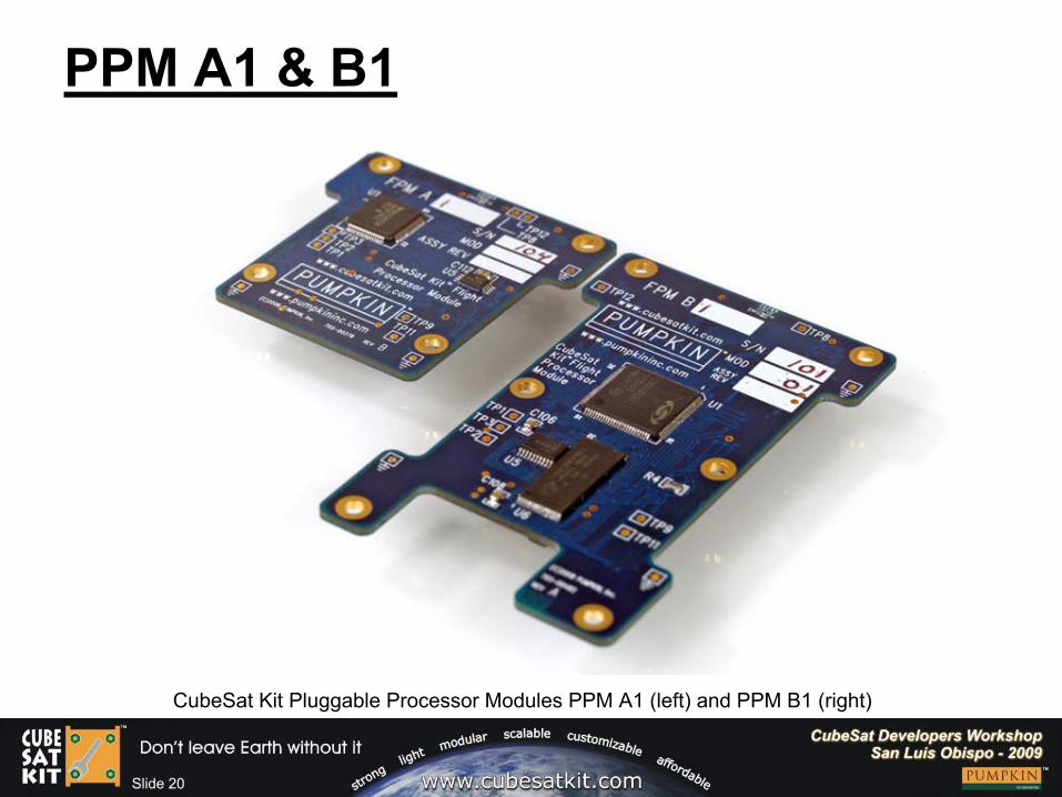
PPM A1 & B1
CubeSat Kit Pluggable Processor Modules PPM A1 (left) and PPM B1 (right)
Slide 21
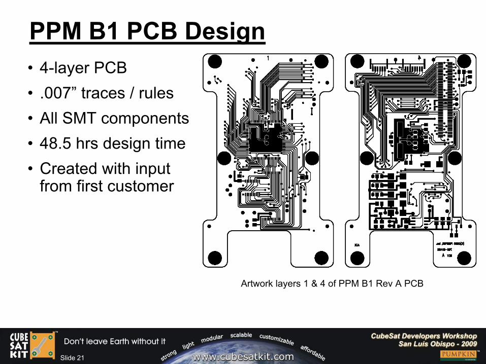
PPM B1 PCB Design• 4-layer PCB• .007” traces / rules• All SMT components• 48.5 hrs design time• Created with input
from first customer
Artwork layers 1 & 4 of PPM B1 Rev A PCB
Slide 22
Review• A PPM designer must resolve, specify and do:
Mechanical interface & packaging constraintsElectrical interface
I/O & bus signalsProgramming / debug (e.g., JTAG)Power & control signals
SchematicsPCB layoutParts procurementAssembly & testSoftware drivers (e.g., SD card)
Slide 23
Conclusions• CSK Hinge design fully vetted, now in production.• Virtually any microprocessor / microcontroller / CPU can
be used on a PPM, subject to volume & power constraints. • Single-chip micros, processors with external memory,
multi-processor systems, DSPs, CPU+SDR, CPU w/TMR Flash memory, etc. are all candidates for PPM integration. If it fits within the physical and power envelope of the open PPM specification, you can fly it!
• Existing software and hardware designs can be ported to the CubeSat Kit with the design of an appropriate PPM.
• Once compatible with the CubeSat Kit, your CubeSat Kit & PPM can utilize other COTS CSK-compatible hardware.
Slide 24
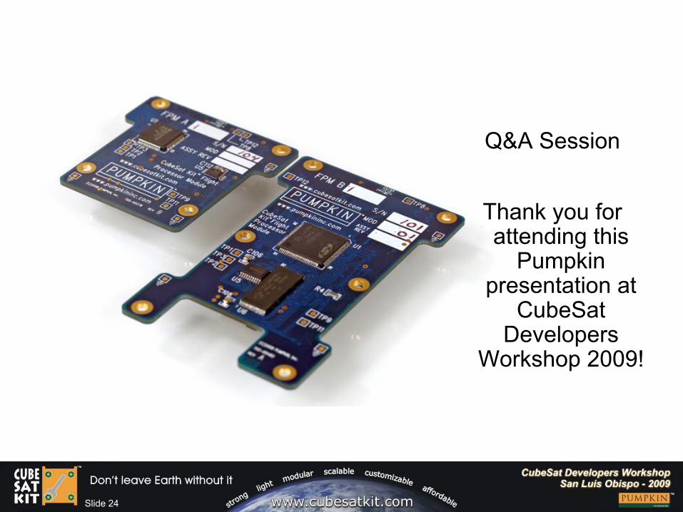
Q&A Session
Thank you for attending this
Pumpkin presentation at
CubeSat Developers
Workshop 2009!
Slide 25
Notice
This presentation is available online in Microsoft®
PowerPoint® and Adobe® Acrobat® formats at:
www.pumpkininc.com/content/doc/press/Pumpkin_CSDWSLO_2009.ppt
and:
www.pumpkininc.com/content/doc/press/Pumpkin_CSDWSLO_2009.pdf
Slide 26
Appendix• Speaker information
Dr. Kalman is Pumpkin's president and chief technology architect. He entered the embedded programming world in the mid-1980's. After co-founding Euphonix, Inc – the pioneering Silicon Valley high-tech pro-audio company – he founded Pumpkin, Inc. to explore the feasibility of applying high-level programming paradigms to severely memory-constrained embedded architectures. He is the creator of the Salvo RTOS and the CubeSat Kit. He holds two United States patents. He is a consulting professor in the Department of Aeronautics & Astronautics at Stanford University and directs the department’s Space Systems Development Laboratory (SSDL). Contact Dr. Kalman at [email protected].
• AcknowledgementsPumpkin’s Salvo and CubeSat Kit customers, whose real-world experience with our products helps us improve and innovate.
• CubeSat Kit informationMore information on Pumpkin’s CubeSat Kit can be found at http://www.cubesatkit.com/.
• Copyright notice© 2000-2009 Pumpkin, Inc. All rights reserved. Pumpkin and the Pumpkin logo, Salvo and the Salvo logo, The RTOS that runs in tiny places, CubeSat Kit, CubeSat Kit Bus, the CubeSat Kit logo and MISC are all trademarks of Pumpkin, Inc. Don’t leave Earth without it is a service mark of Pumpkin, Inc. All other trademarks and logos are the property of their respective owners. No endorsements of or by third parties listed are implied. All specifications subject to change without notice. Unless stated otherwise, all photographs, images and illustrations are the property of Pumpkin, Inc. and may not be used without permission.
First presented at the CubeSat Developers Workshop in San Luis Obispo at Cal Poly University on Friday, April 24, 2009.