purpose of the document -...
TRANSCRIPT
Draft ATC 5301 v01.10.01.05Page i
A Working Group Draft of the Advanced Transportation Controller Joint Committee
ATC 5301 StdUCD v01.10.01.05
Advanced Transportation Controller CabinetUser Comment Draft (StdUCD)
August 14, 2017
StdUCD in support of: ITS Cabinet v2.0 Standard DevelopmentITE Contract: DTFH61-11-D-00052Task 1503
For approval by: Joint Committee on the ATC
For use by: Siva Narla, Chief Engineer and ITS Standards ManagerInstitute of Transportation Engineers
Prepared by: Dave Miller, Chair of the Joint Committee on the ATC
© 2017 AASHTO / ITE / NEMA Do Not Copy Without Written Permission
PLEASE NOTEOnly the PDF copy is the official UCD version. The MS Word document is not to be used or quoted as reference in your comments, only the PDF version is to be copied or quoted for your comments. Do not submit comments integrated into the MS Word document. Comments must be submitted by copying the existing text into the comment spreadsheet along with the proposed changes. Any modifications to this the MS Word version will be dismissed without review as “non-responsive.”
PLEASE NOTEOnly the PDF copy is the official UCD version. The MS Word document is not to be used or quoted as reference in your comments, only the PDF version is to be copied or quoted for your comments. Do not submit comments integrated into the MS Word document. Comments must be submitted by copying the existing text into the comment spreadsheet along with the proposed changes. Any modifications to this the MS Word version will be dismissed without review as “non-responsive.”
PLEASE NOTEOnly the PDF copy is the official UCD version. The MS Word document is not to be used or quoted as reference in your comments, only the PDF version is to be copied or quoted for your comments. Do not submit comments integrated into the MS Word document. Comments must be submitted by copying the existing text into the comment spreadsheet along with the proposed changes. Any modifications to this the MS Word version will be dismissed without review as “non-responsive.”
PLEASE NOTEOnly the PDF copy is the official UCD version. The MS Word document is not to be used or quoted as reference in your comments, only the PDF version is to be copied or quoted for your comments. Do not submit comments integrated into the MS Word document. Comments must be submitted by copying the existing text into the comment spreadsheet along with the proposed changes. Any modifications to this the MS Word version will be dismissed without review as “non-responsive.”
PLEASE NOTEOnly the PDF copy is the official UCD version. The MS Word document is not to be used or quoted as reference in your comments, only the PDF version is to be copied or quoted for your comments. Do not submit comments integrated into the MS Word document. Comments must be submitted by copying the existing text into the comment spreadsheet along with the proposed changes. Any modifications to this the MS Word version will be dismissed without review as “non-responsive.”
PLEASE NOTEOnly the PDF copy is the official UCD version. The MS Word document is not to be used or quoted as reference in your comments, only the PDF version is to be copied or quoted for your comments. Do not submit comments integrated into the MS Word document. Comments must be submitted by copying the existing text into the comment spreadsheet along with the proposed changes. Any modifications to this the MS Word version will be dismissed without review as “non-responsive.”
PLEASE NOTEOnly the PDF copy is the official UCD version. The MS Word document is not to be used or quoted as reference in your comments, only the PDF version is to be copied or quoted for your comments. Do not submit comments integrated into the MS Word document. Comments must be submitted by copying the existing text into the comment spreadsheet along with the proposed changes. Any modifications to this the MS Word version will be dismissed without review as “non-responsive.”
PLEASE NOTEOnly the PDF copy is the official UCD version. The MS Word document is not to be used or quoted as reference in your comments, only the PDF version is to be copied or quoted for your comments. Do not submit comments integrated into the MS Word document. Comments must be submitted by copying the existing text into the comment spreadsheet along with the proposed changes. Any modifications to this the MS Word version will be dismissed without review as “non-responsive.”
Draft ATC 5301 v01.10.01.05Page ii
Ó Copyright 2017AASHTO/ITE/NEMA. All rights reserved.
© 2017 AASHTO / ITE / NEMA Do Not Copy Without Written Permission
Draft ATC 5301 v01.10.01.05Page iii
CHANGE HISTORY
REVISIONSSec Title Author Ver Date Description5.1 Figure 2 D. Miller 1.05 8/14/2017 Added SB1 to CMU in diagram8.5 ATC 5301 StdUCD D. Miller 1.04 8/14/2017 Updated Table 25, Figure 20 per WGAll ATC 5301 StdUCD S. Evans 1.03 8/11/2017 Updated per WG Comment PeriodAll ATC 5301 StdUCD D. Miller 1.02 7/28/2017 Updated per WG Comment PeriodAll ATC 5301 StdPUCD S. Evans 1.01 3/13/2017 Minor updates with tracked changesAll ATC 5301 StdUCD D. Miller 1.00 2/24/2017 Sections below merged into UCD
Draft6.1 Serial Interface Unit D. Miller 1.00 10/7/2010 Brought forward from v1 standard6.2 Model 2202 SP S. Evans 1.20 3/13/2017 ISO/IEC update6.3 Cabinet Monitor Unit S. Evans 1.30 3/13/2017 Data Key change, ISO/IEC update6.4 Model 2216 PS S. Evans 1.20 3/13/2017 fans, startup time6.5 Model 2248 S. Evans 1.00 3/13/2017 Initial Version6.6 Model 2220 ADU S. Evans 1.00 12/14/2016 Initial Version7.1 SIU-2218 Slot D. Miller 1.00 10/17/2010 Brought forward from V1 standard7.2 CMU Slot D. Miller 1.00 10/17/2010 Brought forward from V1 standard7.3 IN Slot D. Miller 1.00 10/17/2010 Brought forward from V1 standard7.4 OUT Slot D. Miller 1.00 10/17/2010 Initial Version (new)8.1 SIU-2218 IN
InterfaceD. Miller 1.00 10/17/2010 Brought forward from V1 standard
8.2 SIU-2218 OUT Interface
D. Miller 1.00 10/17/2010 Brought forward from V1 standard
8.3 SB1 SB2 Interface D. Miller 1.00 10/17/2010 Brought forward from V1 standard8.4 SB3 Interface D. Miller 1.00 10/17/2010 Brought forward from V1 standard8.5 CC Interface D. Miller 1.00 10/17/2010 Brought forward from V1 standard8.6 CDC Interface D. Miller 1.00 10/17/2010 Brought forward from V1 standard8.7 Termination D. Miller 1.00 10/17/2010 Brought forward from V1 standard9.1 SB1 Protocol D. Miller 1.00 10/17/2010 Brought forward from V1 standard9.2 SB2 Protocol D. Miller 1.00 10/17/2010 Brought forward from V1 standard9.3 SB3 Protocol D. Miller 1.00 10/17/2010 Brought forward from V1 standard
© 2017 AASHTO / ITE / NEMA Do Not Copy Without Written Permission

Draft ATC 5301 v01.10.01.05Page iv
NOTICE
Joint NEMA, AASHTO and ITE Copyright andIntelligent Transportation Systems (ITS) Working Group
These materials are delivered "AS IS" without any warranties as to their use or performance.
NEMA, AASHTO, ITE AND THEIR SUPPLIERS DO NOT WARRANT THE PERFORMANCE OR RESULTS YOU MAY OBTAIN BY USING THESE MATERIALS. NEMA, AASHTO, ITE AND THEIR SUPPLIERS MAKE NO WARRANTIES, EXPRESSED OR IMPLIED, AS TO NON-INFRINGEMENT OF THIRD PARTY RIGHTS, MERCHANTABILITY, OR FITNESS FOR ANY PARTICULAR PURPOSE. IN NO EVENT WILL NEMA, AASHTO, ITE OR THEIR SUPPLIERS BE LIABLE TO YOU OR ANY THIRD PARTY FOR ANY CLAIM OR FOR ANY CONSEQUENTIAL, INCIDENTAL, OR SPECIAL DAMAGES, INCLUDING ANY LOST PROFITS OR LOST SAVINGS ARISING FROM YOUR REPRODUCTION OR USE OF THESE MATERIALS, EVEN IF A NEMA, AASHTO OR ITE REPRESENTATIVE HAS BEEN ADVISED OF THE POSSIBILITY OF SUCH DAMAGES. Some states or jurisdictions do not allow the exclusion or limitation of incidental, consequential, or special damages, or exclusion of implied warranties, so the above limitations may not apply to you.
Use of these materials does not constitute an endorsement or affiliation by or between NEMA, AASHTO or ITE, and you, your company, or your products and services.
If you are not willing to accept the foregoing restrictions, you should immediately return these materials.
ATC is a trademark of NEMA, AASHTO and ITE.
© 2017 AASHTO / ITE / NEMA Do Not Copy Without Written Permission
Draft ATC 5301 v01.10.01.05Page v
CONTENTS
Page1 PURPOSE OF THE DOCUMENT....................................................................92 SCOPE OF PROJECT...................................................................................93 REFERENCED DOCUMENTS......................................................................104 CONVENTIONS USED IN THIS DOCUMENT.................................................115 HIGH LEVEL BLOCK DIAGRAM..................................................................11
5.1 ATCC Versions................................................................................................................115.2 Traceability.......................................................................................................................11
6 COMPONENTS.........................................................................................146.1 Model 2218 Serial Interface Unit (SIU)............................................................................14
6.1.1 General...............................................................................................................146.1.2 Model 2218 Functions.........................................................................................146.1.3 Watchdog............................................................................................................146.1.4 Power Up Initialization.........................................................................................146.1.5 Input Functions....................................................................................................146.1.6 Output Functions.................................................................................................176.1.7 Model 2218 Operational Functions.....................................................................176.1.8 Power Requirements...........................................................................................196.1.9 Communications Ports........................................................................................196.1.10 Model 2218 Mechanical Details..........................................................................22
6.2 Model 2202 High Density Switch Pack / Flasher Unit (HDSP/FU)...................................246.2.1 General...............................................................................................................246.2.2 Switch Pack Functions........................................................................................246.2.3 Input Signals.......................................................................................................256.2.4 Output Signals.....................................................................................................266.2.5 Power Requirements...........................................................................................276.2.6 Front Panel Indicators.........................................................................................276.2.7 HDSP Connector.................................................................................................286.2.8 2202 HDSP/FU Mechanical................................................................................29
6.3 Model 2212 Cabinet Monitor Unit.....................................................................................306.3.1 General...............................................................................................................316.3.2 Failed State Action (FSA)....................................................................................316.3.3 Unit Reset...........................................................................................................316.3.4 Exit From Failed State Action..............................................................................316.3.5 Monitor Functions................................................................................................316.3.6 Input Signals.......................................................................................................366.3.7 Control Signal Inputs...........................................................................................376.3.8 Power and Circuit Requirements.........................................................................386.3.9 Failed State Output Circuit..................................................................................396.3.10 Front Panel Indicators.........................................................................................396.3.11 Mechanical..........................................................................................................416.3.12 Serial Bus #3 Terminations.................................................................................426.3.13 Terminal Port.......................................................................................................426.3.14 Serial Memory Key..............................................................................................426.3.15 Serial Memory Key Application Specific Buffer...................................................516.3.16 CMU Connector..................................................................................................51
6.4 Cabinet Power Supply Requirements, High Voltage Versions.........................................526.4.1 Model 2216-HV Cabinet Power Supply...............................................................526.4.2 Model 2217-HV Cabinet Power Supply...............................................................55
6.5 Cabinet Power Supply Requirements, Low Voltage Version............................................57
© 2017 AASHTO / ITE / NEMA Do Not Copy Without Written Permission

Draft ATC 5301 v01.10.01.05Page vi
6.5.1 Model 2248 Cabinet Power Supply.....................................................................576.6 Model 2220 Auxiliary Display Unit....................................................................................59
6.6.1 General...............................................................................................................596.6.2 Mechanical..........................................................................................................596.6.3 Power..................................................................................................................606.6.4 Front Panel Indicators.........................................................................................606.6.5 Front Panel Controls...........................................................................................60
6.7 Sensor Unit......................................................................................................................606.7.1 General...............................................................................................................616.7.2 Form Factor........................................................................................................616.7.3 Connector and Pin Assignments.........................................................................61
7 SLOTS....................................................................................................617.1 Serial Interface Unit Slot..................................................................................................61
7.1.1 General...............................................................................................................617.1.2 Form Factor........................................................................................................617.1.3 Connector and Pin Assignments.........................................................................62
7.2 Cabinet Monitor Unit Slot.................................................................................................627.2.1 General...............................................................................................................637.2.2 Form Factor........................................................................................................637.2.3 Connector and Pin Assignments.........................................................................63
7.3 IN Slot.............................................................................................................................. 637.3.1 General...............................................................................................................637.3.2 Form Factor........................................................................................................647.3.3 Connector and Pin Assignments.........................................................................64
7.4 OUT Slot.......................................................................................................................... 647.4.1 General...............................................................................................................647.4.2 Form Factor........................................................................................................657.4.3 Connector and Pin Assignments.........................................................................65
8 INTERFACES...........................................................................................658.1 SIU IN Interface...............................................................................................................65
8.1.1 General...............................................................................................................668.1.2 Electrical Characteristics.....................................................................................668.1.3 Form Factor........................................................................................................668.1.4 SIU 1 Pin Assignments.......................................................................................66
8.2 SIU OUT Interface...........................................................................................................688.2.1 General...............................................................................................................688.2.2 Electrical Characteristics.....................................................................................688.2.3 Form Factor........................................................................................................688.2.4 Connector Pin Assignments................................................................................69
8.3 SB1/SB2 Interface...........................................................................................................708.3.1 General...............................................................................................................708.3.2 Connector Pin Assignment..................................................................................73
8.4 B3 Interface...................................................................................................................... 738.4.1 General...............................................................................................................738.4.2 SB3 Terminations................................................................................................748.4.3 SB3 Electrical......................................................................................................748.4.4 Form Factor........................................................................................................748.4.5 Connector Pin Assignments................................................................................74
8.5 CC Interface..................................................................................................................... 758.5.1 General...............................................................................................................758.5.2 Form Factor........................................................................................................758.5.3 Connector Pin Assignments................................................................................76
8.6 CDC Interface..................................................................................................................778.6.1 General...............................................................................................................78
© 2017 AASHTO / ITE / NEMA Do Not Copy Without Written Permission
Draft ATC 5301 v01.10.01.05Page vii
8.7 Termination Interface.......................................................................................................798.7.1 General...............................................................................................................798.7.2 Electrical Characteristics.....................................................................................798.7.3 Field Wire Sense.................................................................................................808.7.4 Form Factor........................................................................................................808.7.5 Field Wire Interface.............................................................................................80
9 PROTOCOLS...........................................................................................819.1 SB1 Communications Protocol........................................................................................81
9.1.1 Electrical.............................................................................................................819.1.2 Data Link Layer...................................................................................................819.1.3 Procedures..........................................................................................................819.1.4 Message Timing..................................................................................................819.1.5 SB1 Frame Types...............................................................................................829.1.6 SIU2218 SB1 Frame Types................................................................................849.1.7 CMU2212 SB1 Frame Types..............................................................................94
9.2 SB2 Communications Protocol......................................................................................1069.2.1 General.............................................................................................................1069.2.2 Data Link Layer.................................................................................................1069.2.3 Communication Frames....................................................................................107
9.3 SB3 Communications Protocol......................................................................................1079.3.1 General.............................................................................................................1079.3.2 Serial Bus Terminations....................................................................................1079.3.3 Electrical...........................................................................................................1079.3.4 Data Link Layer.................................................................................................1079.3.5 Procedures........................................................................................................1079.3.6 Message Timing................................................................................................1089.3.7 SB #3 Information Field Formats.......................................................................1089.3.8 2202 HDSP/FU SB3 Frame Types....................................................................1099.3.9 Model 2220 SB3 Frame Types..........................................................................113
10 PRODUCT SAFETY.................................................................................11610.1 Mercury.......................................................................................................................... 11610.2 Shock Hazard................................................................................................................11610.3 Arc Flash........................................................................................................................11610.4 Safe Operation During Service and Replacement.........................................................116
11 ENVIRONMENTAL AND TESTING REQUIREMENTS.....................................11612 ACRONYMS...........................................................................................121
FIGURES
PageFigure 1: ITS Cabinet V2 Major Milestones (http://www.ite.org/standards/ITScabinet/v2.0.asp)......10Figure 2: High Level Functional Block Diagram, High Voltage Version.............................................12Figure 3: High Level Design Functional Block Diagram, Low Voltage Verson..................................13Figure 4: Serial Sensors..........................................................................................................................21Figure 5: Model 2218 Mechanical Dimensions......................................................................................22Figure 6: 2202 HDSP/FU Mechanical Dimensions................................................................................30Figure 7: CMU Mechanical Details.........................................................................................................41Figure 8: Model 2217 Mechanical Details..............................................................................................56Figure 9: model 2218 Slot Mechanical Details......................................................................................62Figure 10: CMU Slot Mechanical Details................................................................................................63Figure 11: IN Slot Mechanical Details....................................................................................................64
© 2017 AASHTO / ITE / NEMA Do Not Copy Without Written Permission
Draft ATC 5301 v01.10.01.05Page viii
Figure 12: OUT Slot Mechanical Details................................................................................................65Figure 13: model 2218 IN Interface Block Diagram...............................................................................66Figure 14: model 2218 OUT Electrical Characteristics.........................................................................68Figure 15: SB1/SB2 Communications Interface Form Factor..............................................................71Figure 16: SB1/SB2 Terminator Unit......................................................................................................72Figure 17: SB3 Communications Interface Form Factor......................................................................74Figure 18: SB3 Communications Cable Form Factor...........................................................................74Figure 19: CC Interface Form Factor......................................................................................................75Figure 20: CC Interface Connection Diagram........................................................................................77Figure 21: CDC Interface Form Factor...................................................................................................78Figure 22: Termination Interface for 2 Load Switch Channels............................................................79Figure 23: Test Profile........................................................................................................................... 119
TABLESPage
Table 1: Address Select Inputs...............................................................................................................16Table 2: Rack Address Frequency.........................................................................................................17Table 3: Input Transition Entry...............................................................................................................18Table 4: Millisecond Counter Rollover Entry.........................................................................................18Table 5: Output Bit Translation..............................................................................................................18Table 6: Model 2218 EIA-232 Port...........................................................................................................23Table 7: Model 2218 Connector Assignments.......................................................................................23Table 8: 2202 HDSP/FU Slot Address....................................................................................................25Table 9: HDFU Mode................................................................................................................................ 26Table 10: HDSP Connector.....................................................................................................................28Table 11: HDFU Mode Connector Pin Assignments.............................................................................29Table 12: CMU Address Inputs...............................................................................................................38Table 13 CMU Serial Memory Key Data.................................................................................................42Table 14: CMU Connector Pin Assignments.........................................................................................51Table 15: Power Supply DC Output Connector.....................................................................................54Table 16: Model 2217 Power Supply DC Output Connector.................................................................56Table 17: Power Supply DC Output Connector.....................................................................................58Table 17: ADU Power Connector Signals..............................................................................................59Table 18: ADU SB #3 Signals..................................................................................................................60Table 19: SIU 1 to IN SLOT Signal Mapping..........................................................................................66Table 20: First Output SIU Opto Assignments......................................................................................69Table 21: model 2218 to OUT SLOT Signal Mapping............................................................................69Table 22: SB1/SB2 Connector Pin Assignment....................................................................................73Table 23: SB #3 Connector Pin Assignment.........................................................................................74Table 25: CC Connector Pin Assignments............................................................................................76Table 25: CDC Connector Pin Assignments.........................................................................................78Table 26: Frame Types and Performance Requirements.....................................................................82Table 27: Module Identification Command...........................................................................................82Table 28: Module Identification Response............................................................................................83Table 29: Type 66 Command.................................................................................................................. 83Table 30: Module Description Command..............................................................................................83Table 31: Module Description Response...............................................................................................83Table 32: Request Module Status Command........................................................................................84Table 33: Request Module Status Response.........................................................................................84Table 34: Millisecond Counter Management Command.......................................................................85Table 35: Millisecond Counter Management Response.......................................................................85Table 36: Configure Inputs Command...................................................................................................85Table 37: Configure Inputs Response...................................................................................................85Table 38: Poll Raw Input Data.................................................................................................................86Table 39: Poll Raw Data Response........................................................................................................86
© 2017 AASHTO / ITE / NEMA Do Not Copy Without Written Permission
Draft ATC 5301 v01.10.01.05Page ix
Table 40: Poll Filtered Data Command..................................................................................................87Table 41: Poll Filtered Data Response...................................................................................................87Table 42: Poll Input Transition Buffer Command..................................................................................87Table 43: Poll Input Transition Buffer Response..................................................................................87Table 44: Set Outputs Command...........................................................................................................88Table 45: Set Outputs Response............................................................................................................88Table 46: Configure Input Tracking Function Command.....................................................................89Table 47: Configure Input Tracking Function Response.....................................................................89Table 48: Configure Complex Outputs..................................................................................................91Table 49: Configure Complex Output Functions Response................................................................92Table 50: Serial Bus #1 Type 80 Command...........................................................................................94Table 51: Serial Bus #1 Type 208 Response.........................................................................................94Table 52: Serial Bus #1 Type 81 Command...........................................................................................94Table 53: Serial Bus #1 Type 81 Response...........................................................................................95Table 54 Type 62 Command.................................................................................................................102Table 55: Type 190 Response...............................................................................................................103Table 56: CMU Type 82 Command.......................................................................................................103Table 57: CMU Type 210 Response......................................................................................................103Table 58: CMU Type 67 Command.......................................................................................................103Table 59: CMU Type 195 Response......................................................................................................104Table 60: SB #3 Frame Types...............................................................................................................108Table 61: SB #3 Type 01 Command.....................................................................................................109Table 62: SB #3 Type 129 Response....................................................................................................109Table 63: SB #3 Type 02 Command.....................................................................................................111Table 64: SB #3 Type 130 Response....................................................................................................111Table 65: SB #3 Type 60 Command.....................................................................................................112Table 66: SB #3 Type 188 Response....................................................................................................112Table 67: SB #3 Type 128 Response....................................................................................................113Table 68: ADU Type 70 Command........................................................................................................113Table 69: ADU Type 70 Response........................................................................................................114Table 70: ADU Type 71 Command........................................................................................................114Table 71: ADU Type 71 Response........................................................................................................115Table 73: Ambient Temperature versus Relative Humidity At Barometric Pressures.....................118
© 2017 AASHTO / ITE / NEMA Do Not Copy Without Written Permission
1 PURPOSE OF THE DOCUMENT
This document is a Standards User Comment Draft (StdUCD) for the Intelligent Transportation System (ITS) Cabinet Version 2 (v2) project under the United States Department of Transportation (USDOT) Work Order T-11001 (ITS Cabinet v2 Maintenance) for development of the ATC 5301 Advanced Transportation Controller Cabinet (ATCC) standard The StdUCD is based on the Concept of Operations (ConOps) adapted from Section 8.4.5 of the "Systems Engineering Guidebook for ITS" (see Section 3 Referenced Documents) with system requirements derived from the user needs identified in the ConOps as a step in the process to create the ATC 5301 ATCC standard. ConOps development began with User Needs presented by the following End Users at the 2008 Workshop in Austin TX:
● Caltrans ● City of Houston TX ● Georgia DOT● Harris County TX ● Kentucky DOT ● Los Angeles DOT● Minnesota DOT ● New York City DOT ● San Francisco MTA
This workshop identified significant additions to User Needs since V1 was published, including:
USDOE ban on the sale of incandescent bulbs used in traffic signal heads EPA mercury waste regulations affecting high-capacity mercury relays State legislation to eliminate shock hazard inside electrical cabinets State legislation to eliminate shock hazard of field wires State legislation to eliminate arc flash hazard under NFPA 70E Need to replace internal components while in flash for motorist safety Low power features to facilitate alternate power sources such as solar panels
This StdUCD provides the detailed description of the elements, interfaces and communications protocols of the ATC 5301 Advanced Transportation Controller Cabinet standard, traceable to the Standards Requirements Specification for:
a) The USDOT Joint Program Office (JPO) who is sponsoring the work;b) The Standard Development Organizations (SDOs) overseeing the development; andc) The consultants, manufacturers, and public transportation professionals who participate in the
committees and working groups (WGs).
2 SCOPE OF PROJECT
The ITS Cabinet V2 project was sponsored by the USDOT JPO as part of an ITS Standards Development Program. The project was performed under the direction of the Advanced Transportation Controller (ATC) Joint Committee (JC). The ATC JC was made up of representatives from three SDOs: the American Association of State Highway and Transportation Officials (AASHTO), the Institute of Transportation Engineers (ITE) and the National Electrical Manufacturers Association (NEMA). The development will be carried out by the ITS Cabinet WG, a technical subcommittee of the ATC JC, and a paid consultant team.
The ITS Cabinet Standard Version 1.02.17b (also known as Version 1 or V1, (see RD[4]) was published in 2006. It defined a transportation field cabinet system (TFCS) that was highly modular and expandable but the standard was missing formalized user needs and requirements that come from the rigor of a Systems Engineering Process (SEP). The objectives of the ITS Cabinet V2 project are as follows:
1) Develop ATC 5301 Advanced Transportation Controller Cabinet standard by assessing issues and integrating lessons learned from current deployments of the ITS Cabinet Standard V1 into a Concept of Operation, Requirements and Design. User needs to be considered, but are not limited to: low-power features, items referred to as "B-List" items by the ITS Cabinet WG, and mercury relay replacement. These items along with all others solicited were introduced into the Systems Engineering Process (see objective #2) that examines their relevancy.
document.docx Page 10 of 123
Draft ATC 5301 v01.10.01.05Page 11
2) Use a systems engineering process to ensure the completeness and correctness of ATC 5301 Advanced Transportation Controller Cabinet standard and associated documents. The standard must be traceable and logically consistent.
3) Develop a detailed conformance statement that addresses backwards compatibility and provides clear and unambiguous instruction on how to extend the standard.
Figure 1: ITS Cabinet V2 Major Milestones (http://www.ite.org/standards/ITScabinet/v2.0.asp)
3 REFERENCED DOCUMENTS
[1] "2008 National Electrical Code," National Fire Protection Association (NFPA), 2008. Available from numerous sources.
[2] “ATC Controller Standard Revision v5.2b,” ATC JC, 26 June 2006. Available from the Institute of Transportation Engineers.
[3] "Electromagnetic Compatibility (EMC) - Part 4-2: Testing and Measurement Techniques - Electrostatic Discharge Immunity Test," IEC 6100-4-2:2008. Available from the International Electrotechnical Commission.
[4] “Intelligent Transportation System (ITS) Standard Specification for Roadside Cabinets v01.02.17b,” ATC JC, 16 November 2006. Available from the Institute of Transportation Engineers.
[5] “NEMA Standards Publication TS 2-2016 v3.07 Traffic Controller Assemblies with NTCIP Requirements," 1 January 2003. Available from National Electrical Manufacturers Association.
[6] "Systems Engineering Guidebook for ITS Version 2.0," FHWA, 2 January 2007. Available from the Federal Highway Administration, California Division.
[7] "Work Order 14-0701 NTCIP and ITE Standards Development," USDOT JPO, 29 May 2007. Available from the Institute of Transportation Engineers.
ITSCabStdUCD_01_10_01_05.docx Page 11
2012-13: HW, SW & Field Installations• Volunteer Effort
2014: Document/Approval• Traceability / Verification• Draft Standard for Ballot
2011: Detailed Design• Volunteer Effort
2010: High Level Design• Houston TX• Open Issues
2009 Requirements• By Working Group
2009 ConOps• Salt Lake City UT
2008 User Needs• Austin TX
ITS Cabinet Version 2 Project
Draft ATC 5301 v01.10.01.05Page 12
[8] “ITS Cabinet V2 StdRS v01.04”, ITS Cabinet Revision 2 Standards Requirements Specification (StdRS)” ATC Cabinet Working Group, 31 January 2011. Available from Institute of Transportation Engineers
[9] “National Electrical Codes (NEC), NFPA 70”, 2014 edition Available from National Fire Protection Association (110.27)
[10] “Model 2070 Controller Standard Version 03”, ATC 5202 v03.04, December 28, 2012. Available from Institute of Transportation Engineers.
[11] “ITS Cabinet V2 Attribute Priorities”, Pillar Consulting Inc, September 23, 2009[12] “Cabinets, Racks, Panels and Associated Equipment”, EIA-310, Electronic Industries Alliance
4 CONVENTIONS USED IN THIS DOCUMENT
RD [nn] indicates Reference Document number nn of REFERENCED DOCUMENTS above Rectangular symbol indicates a physical cabinet element Oval symbol indicates an interface used to connect physical cabinet elements Hatched symbol with dashed border indicates standard does not control mechanical dimensions Solid symbol with solid border indicates standard controls the mechanical dimensions for plug-in
interchangeablity Electrical signals, signal names and signal functions are controlled by the standard in all cases Solid connecting line indicates the standard controls the connector and pin assignments for plug-
in interchangeability. Dashed connecting line indicates the standard does not control the connector type and pin
assignments. The signals are electrically identical among manufacturers, but may require an adapter cable for interchangeability among manufacturers.
5 HIGH LEVEL BLOCK DIAGRAM
5.1 ATCC Versions
The ATCC standard defines two versions: High Voltage (HV) version fulfills the need for operation on traditional 120 VAC service voltage to
control 120 VAC low power (non-incandescent) signal heads Low Voltage (LV) version fulfills the need for operation on 48 VDC alternate power sources, such
as battery and solar, to control low voltage DC signal heads.
The ATCC standard reserves attributes for future version: Very High Voltage (VHV) version fulfills the need for operation on 220 VAC service voltages to
control 240 VAC low power (non-incandescent) signal heads, typically used outside of the USA.
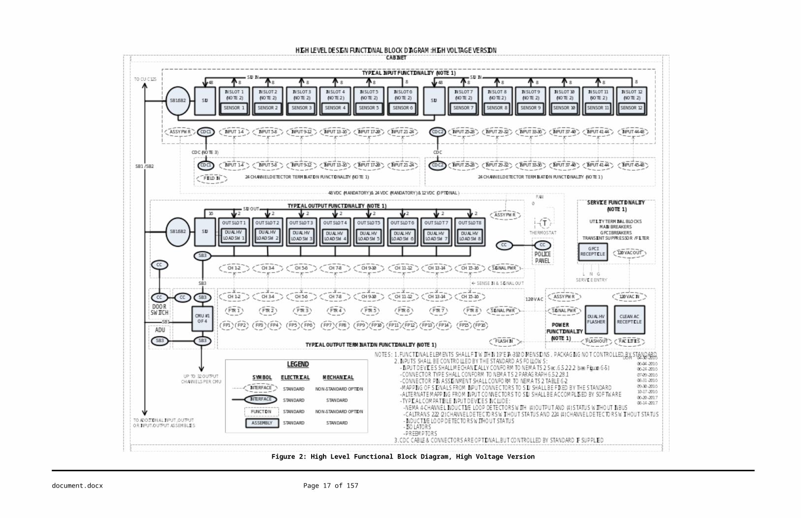
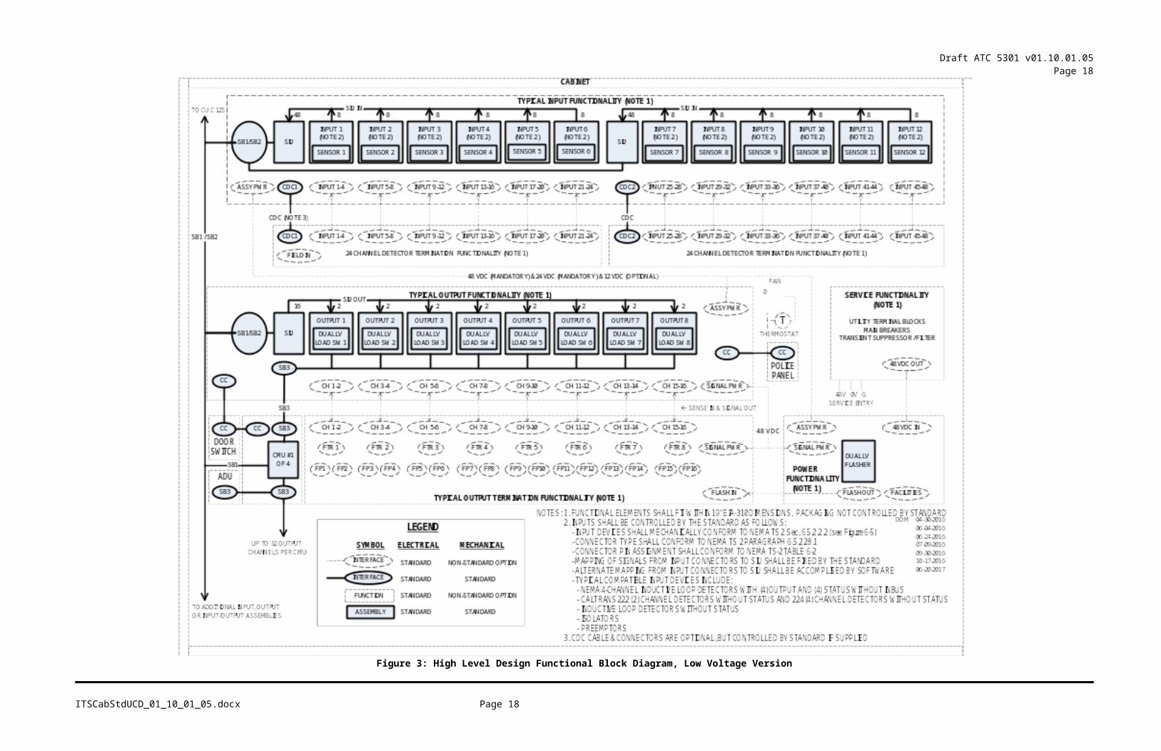
Refer to Figure 2: High Level Functional Block Diagram, High Voltage Version and to Figure 3: High LevelDesign Functional Block Diagram, Low Voltage .
5.2 Traceability
To support traceability from High Level Design to this document, each of the elements and interfaces shown in the Block Diagrams is described in a corresponding section of this standard below.
ITSCabStdUCD_01_10_01_05.docx Page 12

Figure 2: High Level Functional Block Diagram, High Voltage Version
document.docx Page 13 of 123

Draft ATC 5301 v01.10.01.05Page 14
Figure 3: High Level Design Functional Block Diagram, Low Voltage Version
ITSCabStdUCD_01_10_01_05.docx Page 14
Draft ATC 5301 v01.10.01.05Page 15
6 COMPONENTS
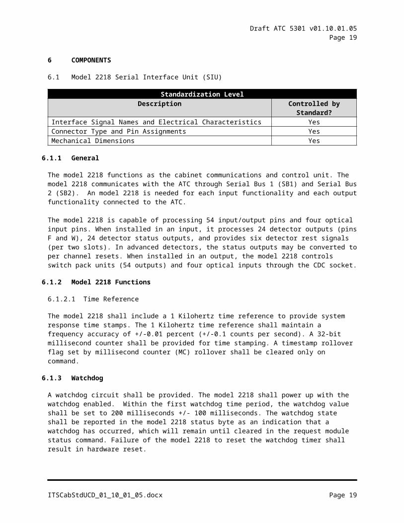
6.1 Model 2218 Serial Interface Unit (SIU)
Standardization LevelDescription Controlled by Standard?
Interface Signal Names and Electrical Characteristics YesConnector Type and Pin Assignments YesMechanical Dimensions Yes
6.1.1 General
The model 2218 functions as the cabinet communications and control unit. The model 2218 communicates with the ATC through Serial Bus 1 (SB1) and Serial Bus 2 (SB2). An model 2218 is needed for each input functionality and each output functionality connected to the ATC.
The model 2218 is capable of processing 54 input/output pins and four optical input pins. When installed in an input, it processes 24 detector outputs (pins F and W), 24 detector status outputs, and provides six detector rest signals (per two slots). In advanced detectors, the status outputs may be converted to per channel resets. When installed in an output, the model 2218 controls switch pack units (54 outputs) and four optical inputs through the CDC socket.
6.1.2 Model 2218 Functions
6.1.2.1Time Reference
The model 2218 shall include a 1 Kilohertz time reference to provide system response time stamps. The 1 Kilohertz time reference shall maintain a frequency accuracy of +/-0.01 percent (+/-0.1 counts per second). A 32-bit millisecond counter shall be provided for time stamping. A timestamp rollover flag set by millisecond counter (MC) rollover shall be cleared only on command.
6.1.3 Watchdog
A watchdog circuit shall be provided. The model 2218 shall power up with the watchdog enabled. Within the first watchdog time period, the watchdog value shall be set to 200 milliseconds +/- 100 milliseconds. The watchdog state shall be reported in the model 2218 status byte as an indication that a watchdog has occurred, which will remain until cleared in the request module status command. Failure of the model 2218 to reset the watchdog timer shall result in hardware reset.
6.1.4 Power Up Initialization
At Power Up, the model 2218 loss of communications timer shall indicate loss of communications until the user program sends the request module status message to reset the “E” bit and a subsequent set output command is processed.
6.1.5 Input Functions
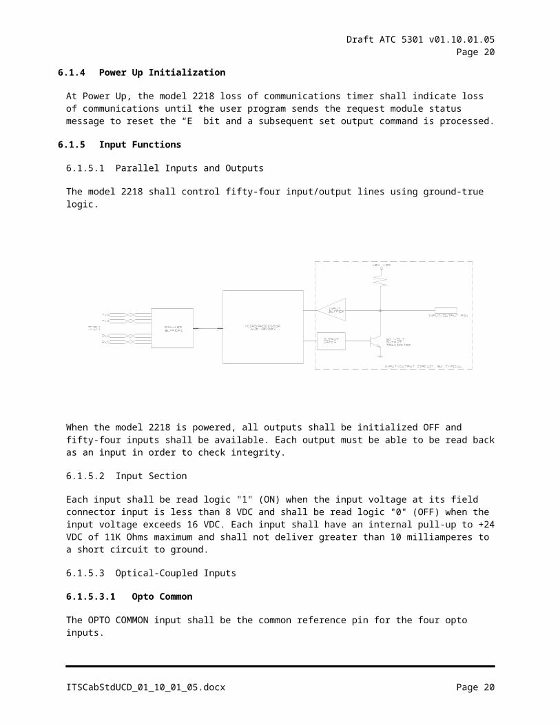
6.1.5.1Parallel Inputs and Outputs
The model 2218 shall control fifty-four input/output lines using ground-true logic.
ITSCabStdUCD_01_10_01_05.docx Page 15
Draft ATC 5301 v01.10.01.05Page 16
When the model 2218 is powered, all outputs shall be initialized OFF and fifty-four inputs shall be available. Each output must be able to be read back as an input in order to check integrity.
6.1.5.2Input Section
Each input shall be read logic "1" (ON) when the input voltage at its field connector input is less than 8 VDC and shall be read logic "0" (OFF) when the input voltage exceeds 16 VDC. Each input shall have an internal pull-up to +24 VDC of 11K Ohms maximum and shall not deliver greater than 10 milliamperes to a short circuit to ground.
6.1.5.3Optical-Coupled Inputs
6.1.5.3.1Opto Common
The OPTO COMMON input shall be the common reference pin for the four opto inputs.
6.1.5.3.2Opto Inputs
The OPTO inputs are intended to provide optical isolation for pedestrian detection, internal cabinet functions, remote interconnect, or other auxiliary inputs. The OPTO inputs are intended to connect through external 27K Ohm, 1-Watt resistors for 120 VAC operations and are intended for direct connection to 12 VAC or 24 VDC (Low True) for pedestrian detector applications.
1. The OPTO inputs shall provide electrical isolation of 10 Megohms minimum resistance and 1000 VAC RMS minimum breakdown to all connector pins except the OPTO COMMON pin, at a maximum breakdown leakage current of 1 milliamperes RMS.
2. The OPTO inputs shall exhibit nominal impedance to the OPTO COMMON pin of 5000 Ohms, +10 percent.
3. The OPTO inputs shall not recognize 3 Volts RMS (AC sinusoid or DC) or less relative to the OPTO COMMON input.
4. The OPTO inputs shall recognize 8 Volts RMS (AC sinusoid or DC) or more relative to the OPTO COMMON input.
5. Any steady state voltage applied between an OPTO input and the OPTO COMMON input shall not exceed 35 VAC RMS.
6. The OPTO inputs shall not be acknowledged when active for 25 milliseconds or less and shall be acknowledged when active for 50 milliseconds or more.
ITSCabStdUCD_01_10_01_05.docx Page 16
Draft ATC 5301 v01.10.01.05Page 17
6.1.5.4 NRESET Input Signal
The model 2218 uses the NRESET input for model 2218 shut down/turn on operations matching the ATC. The model 2218 shall be fully initialized and providing specified operation upon NRESET Line going HIGH (Power Up). The NRESET operation shall cause the model 2218 program restart. No prior message operation data retention is required. The Request Module Status response may report this restart as either a Power On or watchdog. ATC LINESYNC is used as a system time reference. The microprocessor/controller unit shall be reset by any of the following:
1. Pushbutton Reset2. NRESET Signal3. +5 VDC out of regulation4. Microprocessor/controller unit watchdog
6.1.5.5LINESYNC Input Signal
LINESYNC interrupt shall be generated by both the 0-1 and 1-0 transitions of the LINESYNC signal. The LINESYNC interrupt shall monitor the millisecond counter interrupt and set the millisecond counter error flag if there has not been an interrupt from the 1 Kilohertz source for 0.5 seconds (≥60 consecutive LINESYNC interrupts). The LINESYNC interrupt shall synchronize the 1 KHz time reference with the 0-1 transition of the LINESYNC signal once a second. A LINESYNC error flag shall be set if the LINESYNC interrupt has not successfully executed for 0.5 seconds or longer (≥500 consecutive millisecond interrupts).
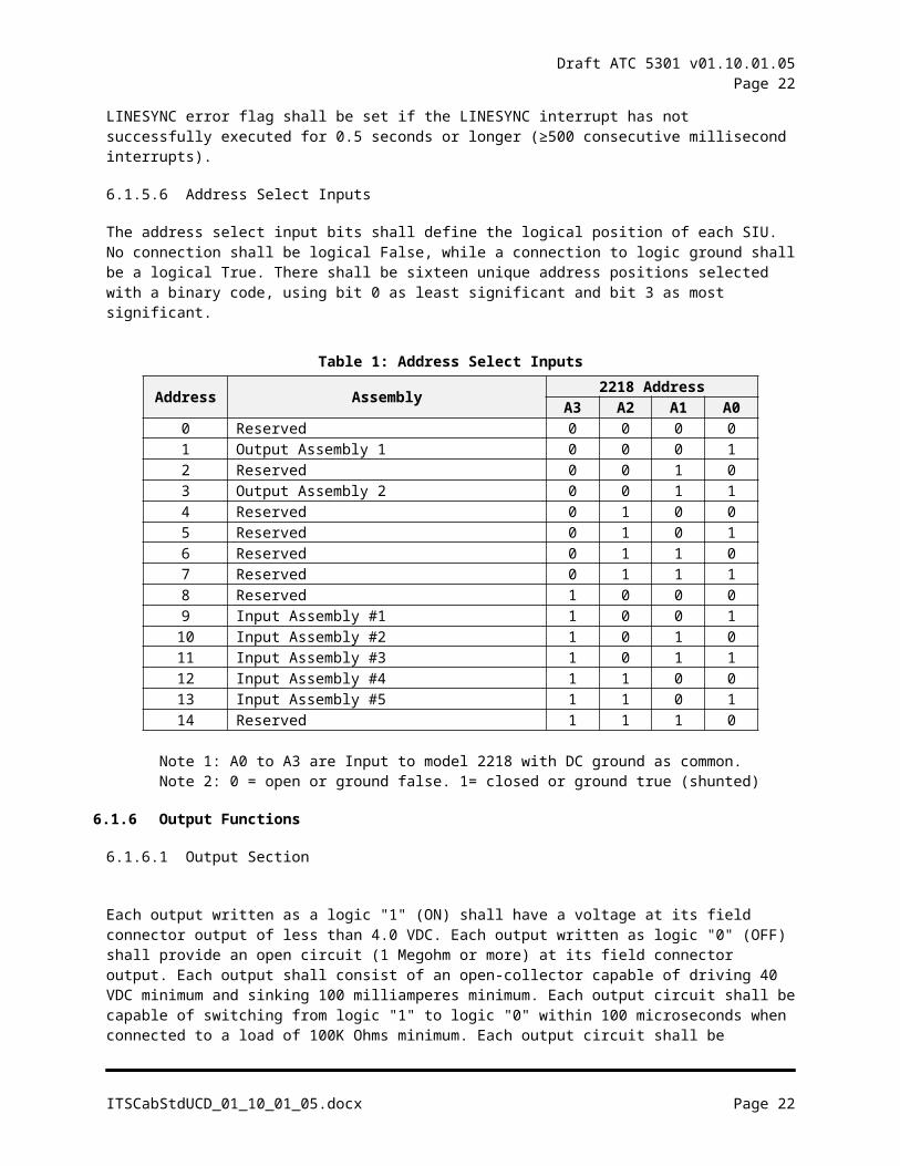
6.1.5.6Address Select Inputs
The address select input bits shall define the logical position of each SIU. No connection shall be logical False, while a connection to logic ground shall be a logical True. There shall be sixteen unique address positions selected with a binary code, using bit 0 as least significant and bit 3 as most significant.
Table 1: Address Select Inputs
Address Assembly 2218 AddressA3 A2 A1 A0
0 Reserved 0 0 0 01 Output Assembly 1 0 0 0 12 Reserved 0 0 1 03 Output Assembly 2 0 0 1 14 Reserved 0 1 0 05 Reserved 0 1 0 16 Reserved 0 1 1 07 Reserved 0 1 1 18 Reserved 1 0 0 09 Input Assembly #1 1 0 0 110 Input Assembly #2 1 0 1 011 Input Assembly #3 1 0 1 112 Input Assembly #4 1 1 0 013 Input Assembly #5 1 1 0 114 Reserved 1 1 1 0
Note 1: A0 to A3 are Input to model 2218 with DC ground as common.Note 2: 0 = open or ground false. 1= closed or ground true (shunted)
ITSCabStdUCD_01_10_01_05.docx Page 17
Draft ATC 5301 v01.10.01.05Page 18
6.1.6 Output Functions
6.1.6.1Output Section
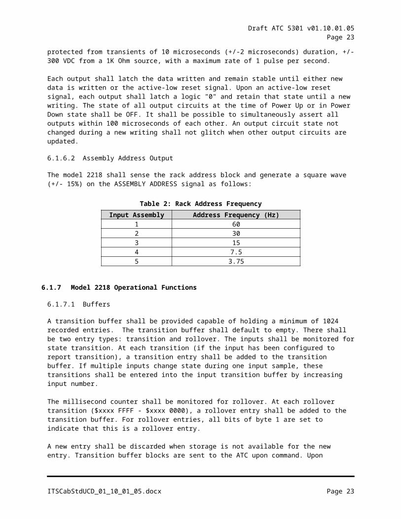
Each output written as a logic "1" (ON) shall have a voltage at its field connector output of less than 4.0 VDC. Each output written as logic "0" (OFF) shall provide an open circuit (1 Megohm or more) at its field connector output. Each output shall consist of an open-collector capable of driving 40 VDC minimum and sinking 100 milliamperes minimum. Each output circuit shall be capable of switching from logic "1" to logic "0" within 100 microseconds when connected to a load of 100K Ohms minimum. Each output circuit shall be protected from transients of 10 microseconds (+/-2 microseconds) duration, +/-300 VDC from a 1K Ohm source, with a maximum rate of 1 pulse per second.
Each output shall latch the data written and remain stable until either new data is written or the active-low reset signal. Upon an active-low reset signal, each output shall latch a logic "0" and retain that state until a new writing. The state of all output circuits at the time of Power Up or in Power Down state shall be OFF. It shall be possible to simultaneously assert all outputs within 100 microseconds of each other. An output circuit state not changed during a new writing shall not glitch when other output circuits are updated.
6.1.6.2Assembly Address Output
The model 2218 shall sense the rack address block and generate a square wave (+/- 15%) on the ASSEMBLY ADDRESS signal as follows:
Table 2: Rack Address FrequencyInput Assembly Address Frequency (Hz)
1 602 303 154 7.55 3.75
6.1.7 Model 2218 Operational Functions
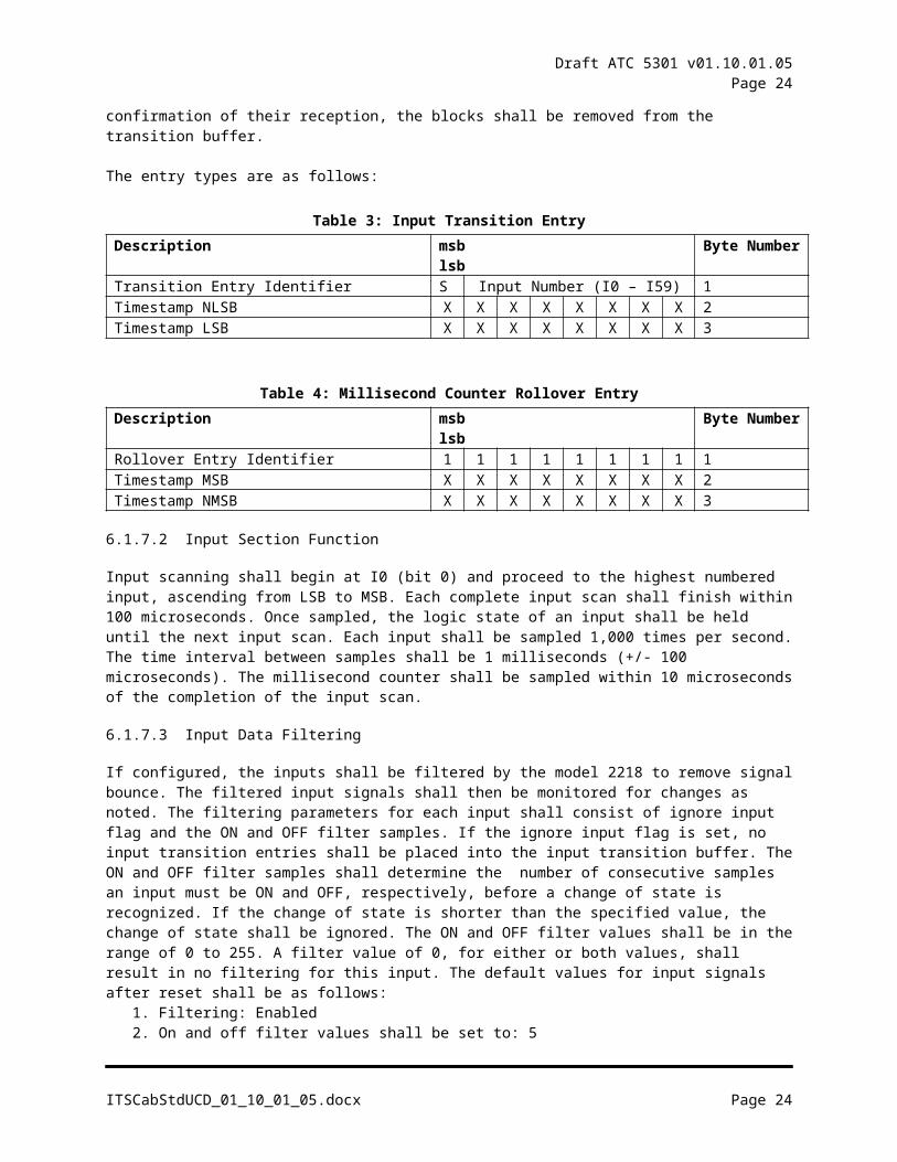
6.1.7.1Buffers
A transition buffer shall be provided capable of holding a minimum of 1024 recorded entries. The transition buffer shall default to empty. There shall be two entry types: transition and rollover. The inputs shall be monitored for state transition. At each transition (if the input has been configured to report transition), a transition entry shall be added to the transition buffer. If multiple inputs change state during one input sample, these transitions shall be entered into the input transition buffer by increasing input number.
The millisecond counter shall be monitored for rollover. At each rollover transition ($xxxx FFFF - $xxxx 0000), a rollover entry shall be added to the transition buffer. For rollover entries, all bits of byte 1 are set to indicate that this is a rollover entry.
A new entry shall be discarded when storage is not available for the new entry. Transition buffer blocks are sent to the ATC upon command. Upon confirmation of their reception, the blocks shall be removed from the transition buffer.
The entry types are as follows:
ITSCabStdUCD_01_10_01_05.docx Page 18
Draft ATC 5301 v01.10.01.05Page 19
Table 3: Input Transition EntryDescription msb lsb Byte NumberTransition Entry Identifier S Input Number (I0 – I59) 1Timestamp NLSB X X X X X X X X 2Timestamp LSB X X X X X X X X 3
Table 4: Millisecond Counter Rollover EntryDescription msb lsb Byte NumberRollover Entry Identifier 1 1 1 1 1 1 1 1 1Timestamp MSB X X X X X X X X 2Timestamp NMSB X X X X X X X X 3
6.1.7.2Input Section Function
Input scanning shall begin at I0 (bit 0) and proceed to the highest numbered input, ascending from LSB to MSB. Each complete input scan shall finish within 100 microseconds. Once sampled, the logic state of an input shall be held until the next input scan. Each input shall be sampled 1,000 times per second. The time interval between samples shall be 1 milliseconds (+/- 100 microseconds). The millisecond counter shall be sampled within 10 microseconds of the completion of the input scan.
6.1.7.3Input Data Filtering
If configured, the inputs shall be filtered by the model 2218 to remove signal bounce. The filtered input signals shall then be monitored for changes as noted. The filtering parameters for each input shall consist of ignore input flag and the ON and OFF filter samples. If the ignore input flag is set, no input transition entries shall be placed into the input transition buffer. The ON and OFF filter samples shall determine the number of consecutive samples an input must be ON and OFF, respectively, before a change of state is recognized. If the change of state is shorter than the specified value, the change of state shall be ignored. The ON and OFF filter values shall be in the range of 0 to 255. A filter value of 0, for either or both values, shall result in no filtering for this input. The default values for input signals after reset shall be as follows:
1. Filtering: Enabled2. On and off filter values shall be set to: 53. Transition monitoring: Disabled (Timestamps are not logged)
6.1.7.4Output Function
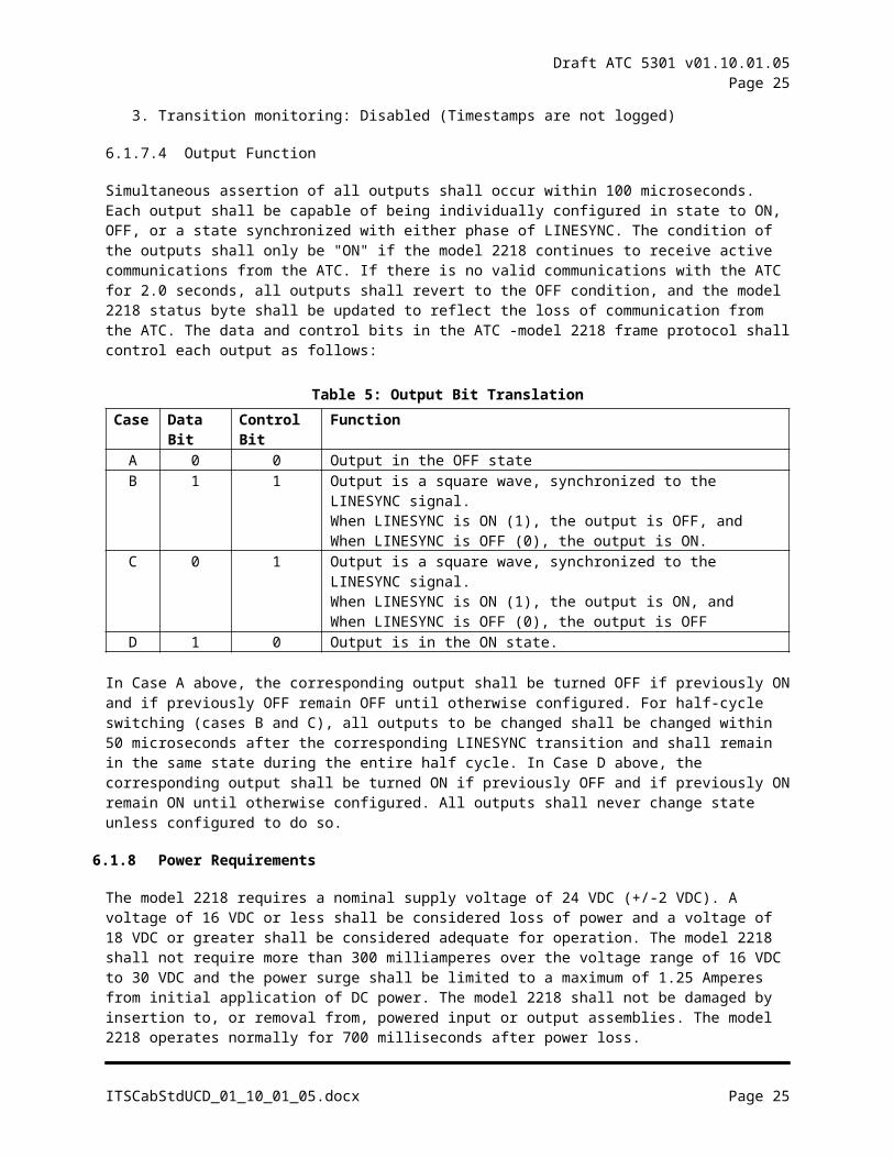
Simultaneous assertion of all outputs shall occur within 100 microseconds. Each output shall be capable of being individually configured in state to ON, OFF, or a state synchronized with either phase of LINESYNC. The condition of the outputs shall only be "ON" if the model 2218 continues to receive active communications from the ATC. If there is no valid communications with the ATC for 2.0 seconds, all outputs shall revert to the OFF condition, and the model 2218 status byte shall be updated to reflect the loss of communication from the ATC. The data and control bits in the ATC -model 2218 frame protocol shall control each output as follows:
Table 5: Output Bit TranslationCase Data Bit Control
BitFunction
A 0 0 Output in the OFF stateB 1 1 Output is a square wave, synchronized to the LINESYNC signal.
When LINESYNC is ON (1), the output is OFF, and When LINESYNC is OFF (0), the output is ON.
C 0 1 Output is a square wave, synchronized to the LINESYNC signal.When LINESYNC is ON (1), the output is ON, and
ITSCabStdUCD_01_10_01_05.docx Page 19
Draft ATC 5301 v01.10.01.05Page 20
When LINESYNC is OFF (0), the output is OFFD 1 0 Output is in the ON state.
In Case A above, the corresponding output shall be turned OFF if previously ON and if previously OFF remain OFF until otherwise configured. For half-cycle switching (cases B and C), all outputs to be changed shall be changed within 50 microseconds after the corresponding LINESYNC transition and shall remain in the same state during the entire half cycle. In Case D above, the corresponding output shall be turned ON if previously OFF and if previously ON remain ON until otherwise configured. All outputs shall never change state unless configured to do so.
6.1.8 Power Requirements
The model 2218 requires a nominal supply voltage of 24 VDC (+/-2 VDC). A voltage of 16 VDC or less shall be considered loss of power and a voltage of 18 VDC or greater shall be considered adequate for operation. The model 2218 shall not require more than 300 milliamperes over the voltage range of 16 VDC to 30 VDC and the power surge shall be limited to a maximum of 1.25 Amperes from initial application of DC power. The model 2218 shall not be damaged by insertion to, or removal from, powered input or output assemblies. The model 2218 operates normally for 700 milliseconds after power loss.
6.1.9 Communications Ports
The model 2218 shall have a minimum of four communications ports, identified as model 2218 Ports SB1, SB2, INBUS and a front panel Terminal port. Communications port SB1 and the Terminal port are connected to the model 2218 microprocessor/controller unit, while Serial ports SB2 and INBUS provide a buffered communications path from the ATC to the intelligent devices in the Input Assembly.
6.1.9.1Model 2218 Port SB#1
Port SB1 shall interface the model 2218 to the CU via Serial Bus 1 (SB1) of the cabinet bus assemblies. See the SB1 Protocol section 9.1 of this standard for the protocol requirements. The SB1 frame address assignments of multiple SIUs are as defined in section 6.1.5.6.
6.1.9.2Model 2218 Port SB#2
Port SB2 shall interface the INBUS port of the model 2218 to the CU via Serial Bus 2 (SB2) of the cabinet bus assemblies. The SB#2 protocol and Data Link parameters to the model 2218 are unspecified and are application specific. INBUS provides a buffered serial interface to intelligent devices located in the Input Assembly.
6.1.9.2.1Synchronous Operation
If the ATC is communicating via logical port SP3S, the model 2218 SB2 shall communicate in HDLC format and protocol, and the hardware requirements shall match serial bus 2 (synchronous TX/RX using TxC from the ATC CPU for common clocking) per ATC 5201 standard.
6.1.9.2.2Asynchronous Operation
If the ATC is communicating via logical port SP3, model 2218 SB2 shall communicate in an asynchronous START BIT / STOP BIT format and protocol per ATC 5201 standard.
ITSCabStdUCD_01_10_01_05.docx Page 20
Draft ATC 5301 v01.10.01.05Page 21
6.1.9.3Terminal Port Operation
The model 2218 Terminal port shall be provided for communication to a personal computer via a front panel 9- position subminiature D-type connector and EIA-232 logic. The model 2218 Terminal port protocol shall be defined by the vendor and operate with vendor-supplied software. The pin assignments of model 2218 port 3 shall be defined by section 6.1.10.5.
6.1.9.4INBUS Operation
The model 2218 INBUS consists of detector rack signal INBUS TxD, INBUS RxD, INBUS TxC and INBUS RxC and shall conform to the electrical standards of EIA-485, single-ended. In this scheme, the RxD- and RxC- inputs of the EIA-485 receivers are connected to 2.5 Volts, while the TxD- and TxC- outputs of the EIA-485 drivers are not used. model 2218 INBUS receivers shall withstand +/-25 Volts, suitable for reception of EIA-232 bipolar signals. All four INBUS signals shall be terminated at each receiver with impedance of 6,800 Ohms (+/-5 percent), connected from signal to +5V ground on the SIU. The protocol shall be defined by the receiving device.
The model 2218 provides one inversion to ensure a SB2 MARK equates to an INBUS MARK. The model 2218 shall provide an LED indicator for TxD and RxD, such that is illuminated during a MARK (START Bit, for example) and extinguished during a SPACE (STOP Bit, for example).
6.1.9.4.1Synchronous Operation
If the ATC is communicating to devices via logical port SP3S, the model 2218 INBUS buffers shall convert model 2218 SB2 TxD+ and TxD- to EIA-485, which shall then be transmitted to the devices via INBUS TxD. Likewise, the model 2218 INBUS buffers shall convert model 2218 SB2 TxC+ and TxC- to EIA-485, which shall then be transmitted to the devices via INBUS TxC.
If the ATC is communicating to detectors via logical port SP3S, the model 2218 INBUS buffers shall convert INBUS RxD from EIA-485, which shall then be transmitted to the ATC via model 2218 SB2 RxD+ and RxD-. Likewise, the model 2218 INBUS buffers shall convert INBUS RxC from EIA-485, which shall then be transmitted to the ATC via model 2218 SB2 RxC+ and RxC-.
6.1.9.4.2Asynchronous Operation
If the ATC is communicating to detectors via logical port SP3, the model 2218 INBUS buffers shall convert model 2218 SB2 TxD+ and TxD- to EIA-485 which shall be transmitted to the detectors via INBUS TxD.
If the ATC is communicating to detectors via logical port SP3, the model 2218 INBUS buffers shall convert INBUS RxD from EIA-485, which shall be transmitted to the ATC via model 2218 SB2 RxD+ and RxD-.
Asynchronous operation shall not use SB2 TxC+, TxC-, RxC+, RxC-, nor INBUS TxC, nor INBUS RxC.
6.1.9.4.3INBUS RTS Input
The INBUS RTS input shall be pulled to +24 Volts via a 10K Ohm resistor on the SIU. In systems using legacy devices that do not use INBUS RTS, this line shall not be used (no connection). Devices equipped with INBUS RTS shall drive this line low when transmitting data from that detector to the model 2218 via INBUS. When not transmitting data, this line shall not be driven low and is pulled to +24V via the 10K Ohm resistor.
ITSCabStdUCD_01_10_01_05.docx Page 21
Draft ATC 5301 v01.10.01.05Page 22
6.1.9.4.4Serial Bus 2 Control
The controller transmits a message on SB2 which shall be received by each device via the model 2218 INBUS TxD and INBUS TxC. If the device is asynchronous, INBUS TxC shall be ignored. Each detector shall compare the address field of the message with its own slot address and assembly address. If the address matches, that device shall respond with data on INBUS RxD and INBUS RxC. If the detector is asynchronous, INBUS RxC shall not be used. The model 2218 of the responding detector shall enable its EIA-485 line drivers to transmit the response from INBUS to SB2. This driver shall be enabled by any of the three following conditions:
Activity on INBUS RxD Activity on INBUS Rx INBUS RTS at low (true)
This driver shall be disabled by either of the following two conditions: Lack of activity on both INBUS RxD and RxC for 1.5 milliseconds
o INBUS RTS transitions from low (true) to high (false)
6.1.9.5 Model 2218 Block Diagrams
6.1.9.5.1Sensors with Serial Ports
Circuitry shown in Exhibit 4-4 shall be included in each SIU, providing a direct serial connection from the controller to each individual serial detector. This serial connection shall be in addition to all of the NEMA CALL and STATUS lines are shown:
Figure 4: Serial Sensors
Detectors and other sensor types that include serial ports can be accessed directly by the Controller Unit via Serial Bus 2 as shown above. The protocol is not dependent upon the SIU. For example, serial detector protocol is installed in the Controller Unit, which then reads the detector CALLs directly from the detector, and the detectors are configured directly from the Controller Unit. The model 2218 circuitry translates the EIA-485 balanced differential signals from the Controller Unit into single-ended signals compatible with modern detectors. In addition, the detectors can be tuned and monitored via the serial bus.
ITSCabStdUCD_01_10_01_05.docx Page 22
Draft ATC 5301 v01.10.01.05Page 23
6.1.10 Model 2218 Mechanical Details
6.1.10.1 Form Factor
The model 2218 module shall be physically composed of a printed circuit board, 4.5 inches high by 6.5 inches long, a front panel 1.42 inches wide by 4.5 inches high with a DIN 96-pin connector on the connector end (opposite the front panel).
Figure 5: Model 2218 Mechanical Dimensions
6.1.10.2 Model 2218 Insertion and Extraction
A “U” handle shall be mounted on the front panel for insertion/extraction.
6.1.10.3 LED Indicators
Six LED waterclear indicators shall be provided on the front panel, as follows: Active Power Serial Bus #1 TxD Serial Bus #1 RxD Serial Bus #2 TxD Serial Bus #2 RxD
The model 2218 power LED shall indicate that the +24 VDC power supply is within regulation. The model 2218 active LED shall be controlled via model 2218 I/O 55. The Serial Bus indicators shall pulse when a frame is correctly received or transmitted.
6.1.10.4 Push Buttons
The model 2218 front panel shall provide a RESET pushbutton that shall provide a hardware RESET to the microprocessor/controller unit.
6.1.10.5 9-Position Subminiature D-Type Connector
The front panel EIA-232 connector is a 9 pin metal shell “DB9S” female subminiature type connector. Because the port is configured as a DTE device, a null modem cable is required to connect directly to a personal computer COMM port.
ITSCabStdUCD_01_10_01_05.docx Page 23
Draft ATC 5301 v01.10.01.05Page 24
Table 6: Model 2218 EIA-232 PortPin # Function I/O
1 RESERVED -2 RECEIVE DATA I3 TRANSMIT DATA O4 RESERVED -5 SIGNAL GROUND X6 RESERVED -7 RESERVED -8 RESERVED -9 RESERVED -
6.1.10.6 Model 2218 Connector
The model 2218 main connector is a three row DIN 4161296 Header Type. Signal names are with respect to the SIU.
Table 7: Model 2218 Connector AssignmentsPin Description Pin Description Pin DescriptionA1 +24 VDC IN B1 +24 VDC IN C1 INPUT / OUTPUT 47A2 INPUT / OUTPUT 0 B2 INPUT / OUTPUT 1 C2 INPUT / OUTPUT 48A3 INPUT / OUTPUT 2 B3 INPUT / OUTPUT 3 C3 INPUT / OUTPUT 49A4 INPUT / OUTPUT 4 B4 INPUT / OUTPUT 5 C4 INPUT / OUTPUT 50A5 INPUT / OUTPUT 6 B5 INPUT / OUTPUT 7 C5 INPUT / OUTPUT 51A6 INPUT / OUTPUT 8 B6 INPUT / OUTPUT 9 C6 INPUT / OUTPUT 52A7 INPUT / OUTPUT 10 B7 INPUT / OUTPUT 11 C7 INPUT / OUTPUT 53A8 INPUT / OUTPUT 12 B8 INPUT / OUTPUT 13 C8 SB1 TXD +A9 INPUT / OUTPUT 14 B9 INPUT / OUTPUT 15 C9 SB1 TXD -A10 INPUT / OUTPUT 16 B10 INPUT / OUTPUT 17 C10 SB1 RXD +A11 INPUT / OUTPUT 18 B11 INPUT / OUTPUT 19 C11 SB1 RXD -A12 INPUT / OUTPUT 20 B12 INPUT / OUTPUT 21 C12 SB1 TXC +A13 INPUT / OUTPUT 22 B13 INPUT / OUTPUT 23 C13 SB1 TXC -A14 INPUT / OUTPUT 24 B14 INPUT / OUTPUT 25 C14 SB1 RXC +A15 INPUT / OUTPUT 26 B15 INPUT / OUTPUT 27 C15 SB1 RXC -A16 INPUT / OUTPUT 28 B16 INPUT / OUTPUT 29 C16 LINESYNC +A17 INPUT / OUTPUT 30 B17 INPUT / OUTPUT 31 C17 LINESYNC -A18 INPUT / OUTPUT 32 B18 INPUT / OUTPUT 33 C18 NRESET +A19 INPUT / OUTPUT 34 B19 INPUT / OUTPUT 35 C19 NRESET -A20 INPUT / OUTPUT 36 B20 INPUT / OUTPUT 37 C20 ASSEMBLY ADRA21 INPUT / OUTPUT 38 B21 INPUT / OUTPUT 39 C21 INBUS RTSA22 INPUT / OUTPUT 40 B22 INPUT / OUTPUT 41 C22 SB2 TXD +A23 INPUT / OUTPUT 42 B23 INPUT / OUTPUT 43 C23 SB2 TXD -A24 INPUT / OUTPUT 44 B24 INPUT / OUTPUT 45 C24 SB2 RXD +A25 INPUT / OUTPUT 46 B25 OPTO INPUT 1 C25 SB2 RXD -A26 OPTO INPUT 2 B26 OPTO INPUT 3 C26 SB2 TXC +
A27 OPTO INPUT 4 B27 OPTO INPUT GROUND C27 SB2 TXC -
A28 ADDRESS – 0 B28 ADDRESS – 1 C28 SB2 RXC +A29 ADDRESS – 2 B29 ADDRESS – 3 C29 SB2 RXC -A30 INBUS TXD B30 INBUS RXD C30 INBUS TXCA31 EQUIPMENT B31 AC LINE C31 INBUS RXC
ITSCabStdUCD_01_10_01_05.docx Page 24
Draft ATC 5301 v01.10.01.05Page 25
Pin Description Pin Description Pin DescriptionGROUND REFERENCE
A32 24 VDC GROUND B32 24 VDC GROUND C32 RESERVED
6.2 Model 2202 High Density Switch Pack / Flasher Unit (HDSP/FU)
Standardization LevelDescription Controlled by Standard?
Interface Signal Names and Electrical Characteristics YesConnector Type and Pin Assignments YesMechanical Dimensions Yes
6.2.1 General
The Model 2202 High-Density Switch Pack / Flasher Unit (HDSP/FU) shall be a modular PCB-based plug-in device providing six solid-state switches (two channels) to drive field signal loads. Each switch shall open or close a connection between applied signal power and external load. The Model 2202 shall operate in either the switch pack mode (HDSP) or the flasher mode (HDFU) depending on the applied SB#3 bus address.
This standard defines both high voltage AC output (2202-HV) and low voltage DC output (2202-LV) units. Unless otherwise specified, all HDSP/FU requirements apply to both output types.
A common form factor, including connector pin-out, is used for both defined units. To prevent possible module or signal head damage should the incorrect version be inserted in a rack, the AC and DC signal power sources from the backplane connector are applied to unique sets of connector pins on the units.
6.2.2 Switch Pack Functions
6.2.2.1Field Output Drivers
The HDSP shall provide two channels consisting of three individual field outputs per channel. The HDFU shall provide two channels consisting of two individual field outputs per channel.
6.2.2.2Field Signal Voltage Sense Inputs
The 2202 HDSP/FU shall monitor the voltages at each of its six sense terminals. All voltage measurements shall be made over an RMS period of 33.3 milliseconds and shall be performed at a minimum sampling rate of 1920 samples per second.
A true RMS voltage measurement shall be made regardless of phase or wave-shape. All 2202-HV HDSP/FU voltage measurements shall be accurate to +/-2%. All 2202-HV HDSP/FU voltage measurements shall include both positive and negative half wave sinusoids, over the voltage range of 0 to 135 Volts RMS. All 2202-LV HDSP/FU voltage measurements shall be accurate to +/-2% over the voltage range of 0 to 64 Volts RMS.
The 2202 HDSP/FU shall be designed such that unused signal inputs are not sensed by the CMU as active signals. The 2202-HV HDSP/FU shall report an unused input at less than 15 Volts RMS when connected to HV+ SIGNAL through 1500 picofarads.
ITSCabStdUCD_01_10_01_05.docx Page 25
Draft ATC 5301 v01.10.01.05Page 26
6.2.2.3Field Load Current Monitor
The 2202 HDSP/FU shall sense the output current independently for each of the six outputs. All current measurements shall be made over an RMS period of 33.3 milliseconds and shall be performed at a minimum sampling rate of 1920 samples per second.
All 2202 HDSP/FU RMS current measurements shall be accurate to +/- 2%. A true RMS current measurement shall be made regardless of phase or wave-shape.
6.2.2.4Diagnostic
If the 2202 HDSP/FU is inoperative due to an internal malfunction, it shall go to a Diagnostic state and force the field outputs to the Off state. A DIAGNOSTIC indicator shall illuminate when the 2202 HDSP/FU is inoperative as a result of a diagnostic fault. The definition of Diagnostic fault is not controlled by the standard, but the Diagnostic state is reported as a bit in the Status byte of the SB#3 response frame, see Table 63 and Table 65.
6.2.3 Input Signals
6.2.3.1Field Signal Control Inputs
A Ground True input (0 VDC to 6 VDC) shall cause the output switch to conduct (ON), and a Ground False (16 VDC or more) shall cause it to not conduct (OFF). State transition shall occur between 6 VDC and 16 VDC. Each input shall not sink more than 20 milliamperes nor be subjected to more than 30 VDC. Each input shall have reverse polarity protection.
6.2.3.22202 HDSP/FU Slot Address
The address select input pins ADDRESS 4:0 define the Serial Bus #3 address of the HDSP mode as shown in Table 8 and the HDFU mode shown in Table 9. The pins are left open for a logical False, and are connected to ADDRESS COMMON for a logical True. ADDRESS COMMON shall be connected only to the ADDRESS 4:0 pins of the same slot. The Serial Bus #3 address is the binary value of the ADDRESS 4:0 inputs plus 1.
Table 8: 2202 HDSP/FU Slot Address
ADDR 4 ADDR 3 ADDR 2 ADDR 1 ADDR 0 SB #3Address Function
False False False False False 0x01 Slot #1 Ch 1,2False False False False True 0x02 Slot #2 Ch 3,4False False False True False 0x03 Slot #3 Ch 5,6False False False True True 0x04 Slot #4 Ch 7,8False False True False False 0x05 Slot #5 Ch 9,10False False True False True 0x06 Slot #6 Ch 11,12False False True True False 0x07 Slot #7 Ch 13,14False False True True True 0x08 Slot #8 Ch 15,16
False True False False False 0x09 Slot #9 Ch 17,18False True False False True 0x0A Slot #10 Ch 19,20False True False True False 0x0B Slot #11 Ch 21,22False True False True True 0x0C Slot #12 Ch 23,24False True True False False 0x0D Slot #13 Ch 25,26False True True False True 0x0E Slot #14 Ch 27,28
ITSCabStdUCD_01_10_01_05.docx Page 26
Draft ATC 5301 v01.10.01.05Page 27
ADDR 4 ADDR 3 ADDR 2 ADDR 1 ADDR 0 SB #3Address Function
False True True True False 0x0F Slot #15 Ch 29,30False True True True True 0x10 Slot #16 Ch 31,32
Table 9: HDFU Mode
ADDR 4 ADDR 3 ADDR 2 ADDR 1 ADDR 0 SB #3Address
Function
True False False False False Reserved
--
True False False False True Reserved
--
True False False True False Reserved
--
True False False True True Reserved
--
True False True False False Reserved
--
True False True False True Reserved
--
True False True True False Reserved
--
True False True True True Reserved
--
True True False False False Reserved
--
True True False False True Reserved
--
True True False True False Reserved
--
True True False True True Reserved
--
True True True False False Reserved
--
True True True False True 0x1E HDFU #1True True True True False 0x1F HDFU #2
True True True True True Reserved
--
6.2.4 Output Signals
6.2.4.1Field Signal Outputs
The 2202 HDSP/FU outputs shall be capable of proper operation with signal power over the Operational Power voltage ranges.
Each individual 2202-HV HDSP/FU output shall be capable of supplying an output current of a minimum of 5 milliamperes to a maximum of 2.0 Amperes RMS to the load. In the 2202-HV HDSP mode, the total output current shall be limited to 1.0 Amperes continuous on all six outputs. In the 2202-HV HDFU mode, the total output current shall be limited to 2.0 Amperes at 50% duty cycle on all four flasher outputs, and
ITSCabStdUCD_01_10_01_05.docx Page 27
Draft ATC 5301 v01.10.01.05Page 28
the Ch 1 and Ch 2 Aux outputs shall be limited to 1.0 Ampere continuous. Each 2202-HV HDSP/FU output shall have a peak stand-off voltage of 500 volts or greater.
Each individual 2202-LV HDSP/FU output shall be capable of supplying an output current of a minimum of 5 milliamperes to a maximum of 3.0 Amperes RMS to the load. In the 2202-LV HDSP mode, the total output current shall be limited to 2.0 Amperes continuous on all six outputs. In the 2202-LV HDFU mode, the total output current shall be limited to 3.0 Amperes at 50% duty cycle on all four flasher outputs, and the Ch 1 and Ch 2 Aux outputs shall be limited to 2.0 Amperes continuous. Each 2202-LV HDSP/FU output shall have a peak stand-off voltage of 100 volts or greater.
Each switch shall have an OFF state dv/dt rating of 100 Volts per microsecond or better. Each switch shall provide isolation between control inputs and field outputs of at least 2000 VDC and at least 100 megohms resistive.
6.2.4.1.1Off-State Leakage
When the switch is in the OFF state, the output current through the load shall not exceed 1 milliampere maximum.
6.2.4.1.2Zero-Cross
The 2202-HV HDSP/FU output shall turn On within 10 degrees of the zero voltage point of the AC Line sinusoid on the first turn-on cycle. All subsequent cycles shall turn On within 5 degrees of the zero voltage point of the AC line sinusoid. The output shall turn On within one half cycle following the application of the input signal. The output shall turn Off within 5 degrees of the zero voltage point of the AC line sinusoid and within one half cycle following the removal of the input signal.
6.2.5 Power Requirements
6.2.5.1 Operational Power
The 2202 HDSP/FU shall commence normal operation within 500 ms of application of nominal power. The Field Outputs shall not glitch to the On state during this period. Surge current drawn from the +24VDC source during power-up shall not exceed 100 mA peak. Surge current drawn from the HV+MAINS or LV+MAINS source during power-up shall not exceed 2000 mA peak.
6.2.5.1.1HV+MAINS
The HV+MAINS input provides operational power to the 2202-HV HDSP/FU. The 2202-HV HDSP/FU shall be operational over the voltage range of 60 Volts AC to 135 Volts AC.
6.2.5.1.2HV+SIGNAL
The HV+SIGNAL input provides field signal power to the 2202-HV HDSP/FU. This input shall be driven by the output of the Main Contactor secondary. The 2202-HV HDSP/FU field signal outputs shall be operational over the voltage range of 60 Volts AC to 135 Volts AC.
6.2.5.1.3LV+MAINS
The LV+MAINS input provides operational power to the 2202-LV HDSP/FU. The 2202-LV HDSP/FU shall be operational over the voltage range of 18 Volts RMS to 60 Volts RMS.
ITSCabStdUCD_01_10_01_05.docx Page 28
Draft ATC 5301 v01.10.01.05Page 29
6.2.5.1.4LV+SIGNAL
The LV+SIGNAL input provides field signal power to the 2202-LV HDSP/FU. This input shall be driven by the output of the Main Contactor secondary. The 2202-LV HDSP/FU field signal outputs shall be operational over the voltage range of 18 Volts RMS to 60 Volts RMS.
6.2.5.2+24VDC Power Supply
The maximum current into the +24 VDC input pin over the voltage range of 0 VDC to 30 VDC shall be less than 60 milliamperes.
6.2.6 Front Panel Indicators
All indicators shall be clear LEDs. Clear LEDs shall not depend on a reflector or diffusion as part of its design. Clear LEDs shall not appear to be ON when exposed to ambient light. The following indicators shall be provided:
6.2.6.1Power
A green POWER indicator shall illuminate to indicate Operational input voltage (HV+MAINS or LV-MAINS) is proper.
6.2.6.2Diagnostic
A red DIAGNOSTIC indicator shall illuminate when the 2202 HDSP/FU is in inoperative as a result of a diagnostic condition.
6.2.6.3SB #3 Rx
A yellow indicator shall pulse On each time the 2202 HDSP/FU correctly receives a frame on Serial Bus #3 from the CMU-2212.
6.2.6.4SB #3 Tx
A yellow indicator shall pulse ON each time the 2202 HDSP/FU transmits a frame on Serial Bus #3 to the CMU-2212.
6.2.6.5Field Signal Control Input
An individual red, yellow, and green LED indicator shall illuminate when the Field Signal Control input is active. There shall be one indicator for each Control input of each channel.
6.2.6.6Channel ID Status (HDSP mode)
Two blue LED indicators shall be provided for each channel and shall illuminate based on the command Frame #01 data from the CMU-2212. These Channel ID Status indicators may be used by the CMU-2212 to indicate various status conditions based on an 2202 HDSP/FU channel.
6.2.6.7Flasher Channel Status (HDFU mode)
Two LED indicators shall be provided for each flasher channel and shall illuminate to indicate an active Flasher output. The voltage level of the FL#x-x SENSE input is used to determine the active status of the LEDs such that they reflect actual flasher status to the field.
ITSCabStdUCD_01_10_01_05.docx Page 29
Draft ATC 5301 v01.10.01.05Page 30
6.2.6.7.1Flasher Channel Status Thresholds (HDFU-HV mode)
The Flasher output status shall be On when the RMS voltage exceeds 70 Vrms. The Flasher output status shall be Off when the RMS voltage is less than 50 Vrms.
6.2.6.7.2Flasher Channel Status Thresholds (HDFU-LV mode)
The Flasher output status shall be On when the RMS voltage exceeds 44 Vrms. The Flasher output status shall be Off when the RMS voltage is less than 40 Vrms.
6.2.7 HDSP Connector
The 2202 HDSP/FU shall connect to the OA2 backplane using a male DIN 41612 Type E series, 48-pin connector. The Rx and Tx signal names are with respect to the 2202 HDSP/FU. The connector pin assignments for the HDSP mode are shown in Table 10:
Table 10: HDSP Connector
Pin #
A (Bottom Row) C (Middle Row)
E (Top Row)
2 Ch 1 Red In Ch 1 Yellow In Ch 1 Green In4 Ch 2 Red In Ch 2 Yellow In Ch 2 Green In6 +24VDC VDC Ground Address 48 Equipment Ground MAINS Ground MAINS Ground10 SB #3 Rx+ SB #3 Tx+ Address Common12 SB #3 Rx- SB #3 Tx- Address 314 Address 0 Address 1 Address 216 Ch 1 Red Sense Ch 1 Red Out Ch 1 Red Out18 Ch 1 Yellow Sense Ch 1 Yellow Out Ch 1 Yellow Out20 Ch 1 Green Sense Ch 1 Green Out Ch 1 Green Out22 Ch 2 Red Sense Ch 2 Red Out Ch 2 Red Out24 Ch 2 Yellow Sense Ch 2 Yellow Out Ch 2 Yellow Out26 Ch 2 Green Sense Ch 2 Green Out Ch 2 Green Out28 LV+ Signal LV+ Signal LV+ Signal30 HV+ Signal HV+ Signal HV+ Signal32 LV+ MAINS MAINS Ground HV+ MAINS
The connector pin assignments for the HDFU mode are shown in Table 11
Table 11: HDFU Mode Connector Pin Assignments
Pin #
A (Bottom Row) C (Middle Row)
E (Top Row)
2 Reserved Reserved Ch 1 Aux In4 Ch 2 Aux In Reserved Reserved6 +24VDC VDC Ground Address 48 Equipment Ground MAINS Ground MAINS Ground10 SB #3 Rx+ SB #3 Tx+ Address Common12 SB #3 Rx- SB #3 Tx- Address 314 Address 0 Address 1 Address 216 FL#1-1 Sense FL#1-1 Out FL#1-1 Out
ITSCabStdUCD_01_10_01_05.docx Page 30
Draft ATC 5301 v01.10.01.05Page 31
Pin #
A (Bottom Row) C (Middle Row)
E (Top Row)
18 FL#1-2 Sense FL#1-2 Out FL#1-2 Out20 Ch 1 Aux Sense Ch 1 Aux Out Ch 1 Aux Out22 Ch 2 Aux Sense Ch 2 Aux Out Ch 2 Aux Out24 FL#2-1 Sense FL#2-1 Out FL#2-1 Out26 FL#2-2 Sense FL#2-2 Out FL#2-2 Out28 LV+ Signal LV+ Signal LV+ Signal30 HV+ Signal HV+ Signal HV+ Signal32 LV+ MAINS MAINS Ground HV+ MAINS
6.2.8 2202 HDSP/FU Mechanical
The 2202 HDSP/FU shall be 1.12” W x 4.50” H x 6.50” D. Mechanical details are illustrated Figure 6.
The 2202 HDSP/FU shall slide into two card guides in the High-Density Output Assembly (OA2), each having a nominal slot width of 0.075” and a maximum slot depth of 0.125”. The nominal thickness of the 2202 HDSP/FU PCB shall be 0.062” +/- 10%. The maximum height of components used on the 2202 HDSP/FU shall be 1.0”. The handle shall not extend further than 1.30” from the front panel surface.
ITSCabStdUCD_01_10_01_05.docx Page 31
Draft ATC 5301 v01.10.01.05Page 32
Figure 6: 2202 HDSP/FU Mechanical Dimensions
6.3 Model 2212 Cabinet Monitor Unit
Standardization LevelDescription Controlled by Standard?
Interface Signal Names and Electrical Characteristics YesConnector Type and Pin Assignments YesMechanical Dimensions Yes
ITSCabStdUCD_01_10_01_05.docx Page 32
Draft ATC 5301 v01.10.01.05Page 33
6.3.1 General
The Cabinet Monitor Unit (CMU) is the principle part of the ATC Cabinet monitoring system. The role of the CMU is to query various cabinet conditions and, if the application requires action, the CMU will transfer control from the ATC to a flashing control mode.
The Model 2212 CMU is composed of a microprocessor, memory devices including non-volatile memory, communications circuitry to interface with Serial Buses #1 and #3, front panel indicators, front panel communication connector and a serial memory key device. The operating program shall be resident in the non-volatile memory. The serial memory key shall possess the conditions and function selections of the CMU.
6.3.2 Failed State Action (FSA)
Only Unit Reset shall reset the CMU from a LATCHED FAILED STATE ACTION (LFSA). Only a Unit Reset or a CMU Power Fail shall reset a LATCHED RESETTABLE FAILED STATE ACTION (LFSA-R). A NONLATCHED FAILED STATE ACTION (NFSA) shall be reset if the fault conditions causing the NFSA have been removed. An NFSA shall last for the programmed Minimum Flash time at a minimum. Only one LFSA, LFSA-R or NFSA fault state shall be set at any time.
6.3.3 Unit Reset
The CMU shall be reset from a FSA as a result of the front panel reset button or the EXTERNAL TEST RESET input. This reset command shall be a one-time event, such that a continuous reset command does not prevent the CMU from operating.
The EXTERNAL TEST RESET input shall be True when the voltage is less than 8 VDC. The EXTERNAL TEST RESET input shall be False when the voltage is greater than 16 VDC. A minimum True pulse width on the EXTERNAL TEST RESET input of 100 milliseconds shall be required for a Unit Reset. The EXTERNAL TEST RESET input shall be referenced to VDC GROUND.
6.3.4 Exit From Failed State Action
Prior to the CMU transferring the output relay contacts from the Fault state to the No Fault state, a transition period of 500 milliseconds shall occur. During the transition period the output relay contacts shall be in the Fault state and the CMU shall set the Start-Up Flash Call bit in the Type 209 Frame to 1. At all other times the Start-Up Flash Call bit of the Type 209 Frame shall be set to 0.
6.3.5 Monitor Functions
6.3.5.1Cabinet Power Supply
The CMU shall sense the Cabinet +24 VDC and +12 VDC power supply sources to +/- 5 percent accuracy. The CMU shall also sense the Cabinet +24 VDC state in each Output Assembly as reported by each HDSP. Voltages equal to or greater than +22 VDC and +11 VDC respectively shall NOT cause a LFSA. Voltages at or less than +18 VDC and +9 VDC for 500 milliseconds or longer shall cause a LFSA. If the sensed voltage is less than +22 VDC or +11 VDC for 200 milliseconds or less, the CMU shall NOT cause a LFSA. All other timing or voltage conditions may or may not cause LFSA. A +24 VDC failure or +12 VDC failure during the programmed Minimum Flash time or during a CMU Power Failure shall not cause a LFSA. The CMU shall report the value of the +24 VDC and +12 VDC power supply sources in the Type 209 response frame.
There shall be programming in the serial memory key to disable +12 VDC power supply monitoring.
ITSCabStdUCD_01_10_01_05.docx Page 33
Draft ATC 5301 v01.10.01.05Page 34
6.3.5.2Conflicting Channels
For purpose of conflict determination, an active signal on either of the Green/Walk or Yellow inputs associated with any of the 32 channels shall be considered as that channel being active. The serial memory key shall contain the permissive channel pair programming. When any conflicting channels are detected as concurrently active for less than 200 milliseconds, the CMU shall not cause a LFSA. When any conflicting channels are detected as concurrently active for 500 milliseconds or more, the CMU shall cause a LFSA. When any conflicting channels are detected as concurrently active for more than 200 milliseconds but less than 500 milliseconds, the CMU may or may not cause a LFSA. The time interval between the beginning of the concurrently conflicting channels and the transfer to the LFSA shall not exceed 500 milliseconds.
6.3.5.3Serial Bus Error
The CMU communicates using both Serial Buses (SB) #1 and #3. On SB #1, the CMU is a secondary, polled by the ATC primary. On SB #1, the CMU shall respond to the SB #1 address defined by the ADDRESS 0 and ADDRESS 1 pins. On SB #3, the CMU is the primary, polling each high density switch pack (HDSP) and high density flasher unit pack (HDFU) secondary device.
6.3.5.3.1Serial Bus #1 Error
The CMU shall cause a FSA when a Type 81 or Type 67 frame has not been received from the ATC for greater than 600 milliseconds. The first and second failures in a 24-hour period shall be a NFSA. The third failure in a 24-hour period shall be a LFSA-R. If a CMU Power Fail resets the LFSA-R, the SB #1 timeout count shall be reset to 2 such that the next SB #1 timeout results in a LFSA-R.
An SB #1 timeout failure during the programmed minimum flash time or during a CMU power failure shall not cause a FSA. The SB #1 timeout function shall be disabled if the SB #1 DISABLE input is at a True (Low) state. The SB #1 DISABLE input shall be True when the voltage is less than 8 VDC. The SB #1 DISABLE input shall be False when the voltage is greater than 16 VDC. The SB #1 DISABLE input shall be referenced to VDC GROUND.
6.3.5.3.2Serial Bus #3 Error
The CMU shall cause a FSA when a Type 129 or Type 130 Frame has not been received from each HDSP for greater than 300 milliseconds. The first and second failures in a 24-hour period shall be a NFSA. The third failure in a 24-hour period shall be a LFSA-R. If a CMU power fail resets the LFSA-R, the SB #3 timeout count shall be reset to 2 such that the next SB #3 timeout results in a LFSA-R. A SB #3 timeout failure during the programmed minimum flash time or during a CMU power failure shall not cause a FSA.
6.3.5.4Type 62 – Send to Local Flash Command Message
If the “N” bit is set in a Type 62 – Send to Local Flash Command message, the CMU shall react by causing a NFSA. The NFSA shall remain until the receipt of a Type 62 – Send to Local Flash Command message with the “N” bit cleared or until the CMU is reset by a unit reset or CMU power fail. The NFSA shall last for the programmed minimum flash time at a minimum. If the “L” bit is set in a Type 62 – Send to Local Flash Command message, the CMU shall react by causing a LFSA.
6.3.5.5Diagnostics
6.3.5.5.1Diagnostic Error
ITSCabStdUCD_01_10_01_05.docx Page 34
Draft ATC 5301 v01.10.01.05Page 35
The CMU shall be provided with a resident series of self-check diagnostic capabilities. The CMU shall contain provisions to verify all memory elements on power-up. When a fault is detected, the LFSA-R shall be set and the DIAGNOSTIC indicator illuminated.
6.3.5.5.2RAM Diagnostic
This test shall verify that all RAM elements are operating correctly at power-up or following a Unit Reset. Patterns shall be written to RAM. Each write shall be followed by a read to verify that it contains the written pattern.
6.3.5.5.3Nonvolatile Diagnostic
This test shall verify that the nonvolatile ROM(s) contain the proper program. The routine shall perform a check on each ROM and make a comparison with a preprogrammed check value. This test shall be performed at power-up and at a minimum rate of 1024 bits per second during operation.
6.3.5.5.4Serial Memory Key Memory Diagnostic
This test shall verify whether the non-volatile serial memory key contains valid data and that the data has not changed since the last write. The routine shall perform a check on each nonvolatile memory element at power-up and whenever read and make a comparison with a preprogrammed check value as described in section 6.3.14. The serial memory key not present shall cause a LFSA if the DOOR SWITCH FRONT input is sensed as not active (door closed).
6.3.5.5.5Internal MPU Monitor
The CMU shall monitor the operation of its microprocessor with an independent circuit. At a minimum, the monitoring circuit shall receive logic state transitions at least once every 50 milliseconds from the microprocessor. When the logic state transition is not received for 500 milliseconds the monitor circuit shall force a LFSA-R and illuminate the DIAGNOSTIC indicator.
6.3.5.6Multiple Input
The CMU shall be capable of monitoring for the presence of an active signal on two or more inputs of a channel. When the presence of an active signal on two or more inputs of a channel is detected for less than 200 milliseconds, the CMU shall not cause a LFSA. When the presence of an active signal on two or more inputs to a channel is detected for 450 milliseconds or more, the CMU shall cause a LFSA. When the presence of an active signal on two or more inputs to a channel is detected for more than 200 milliseconds but less than 450 milliseconds, the CMU may or may not cause a LFSA. Multiple Indication monitoring shall be disabled when the MAIN CONTACTOR COIL STATUS input is not active. There shall be programming in the serial memory key to disable Multiple Input monitoring on a color combination basis (G+Y, Y+R, G+R).
6.3.5.7Lack of Signal Inputs
The CMU shall be capable of monitoring for the absence of any required signal voltage OR signal load current (CSU) on the inputs of a channel. For voltage purposes a required signal on the Green or Yellow or Red inputs associated with a channel shall be considered as that channel being active. For current purposes, a load current value that exceeds the programmed threshold shall be considered as that output being active.
When an absence of an active channel (voltage OR output current) is detected for less than 1200 milliseconds, the CMU shall not cause a LFSA. When an absence of an active channel is detected for 1500 milliseconds or more, the CMU shall cause a LFSA. When an absence of an active channel is detected for more than 1200 milliseconds but less than 1500 milliseconds, the CMU may or may not
ITSCabStdUCD_01_10_01_05.docx Page 35
Draft ATC 5301 v01.10.01.05Page 36
cause a LFSA. Lack of Signal Input monitoring shall be disabled for all channels when the MAIN CONTACTOR COIL STATUS input is not active. There shall be programming in the serial memory key to disable Lack of Signal Input monitoring on a per channel basis.
Lack of Signal Input monitoring shall also be disabled for any channel which has the DARK CHANNEL MAP bit set to "1" in the serial memory key programming for the DARK CHANNEL MAP addressed by the DARK CHANNEL MAP SELECT bits in a Type 81 message.
6.3.5.8Minimum Yellow Clearance
The CMU shall verify that the Yellow Change interval is at least 2.7 seconds (+/-0.1 seconds). When the minimum Yellow Change interval is not satisfied, the CMU shall cause a LFSA. The CMU shall report a Skipped Yellow Clearance when the Yellow Change interval is less than 100 milliseconds. The CMU shall report a Short Yellow Clearance when the Yellow Change interval is less than 2.7 seconds (+/-0.1 seconds) and greater than 100 milliseconds.
Minimum Yellow Change interval monitoring shall be disabled when the MAIN CONTACTOR COIL STATUS input is not active. There shall be programming in the serial memory key to disable Minimum Yellow Change interval monitoring on a per channel basis.
6.3.5.9Minimum Yellow Plus Red Clearance
The CMU shall verify that the Yellow Change plus Red Clearance interval between the end of an active GREEN signal and the beginning of the next conflicting GREEN signal is at least 2.7 (+/-0.1 seconds). When the minimum Yellow Change plus Red Clearance interval is not satisfied, the CMU shall cause a LFSA.
Minimum Yellow Change plus Red Clearance monitoring shall be disabled when the MAIN CONTACTOR COIL STATUS input is not active. There shall be programming in the serial memory key to disable Minimum Yellow Change plus Red Clearance interval monitoring on a per channel basis.
6.3.5.10 Flashing Yellow Arrow
A minimum of six Flashing Yellow Arrow channel pairs shall be supported by the CMU. Programming shall be provided in the serial memory key to specify the Overlap channel, Protected Left Turn channel, and the Opposing Thru channel. Any of the 32 CMU channels may be selected for the FYA operation including Virtual channels.
6.3.5.11 Local Flash Status
The CMU shall monitor the LF STATUS input. When this signal is sensed as not active for greater than 350 milliseconds, the CMU shall cause a NFSA. When this signal is sensed as not active for less than 200 milliseconds, the CMU shall not cause a NFSA.
6.3.5.11.1 Local Flash Status Recovery
Recovery from Local Flash Status NFSA shall occur when this signal is sensed as active for greater than 350 milliseconds. When this signal is sensed as active for less than 200 milliseconds, the CMU shall not cause recovery from Local Flash Status NFSA.
6.3.5.12 Circuit Breaker Trip Status
The CMU shall monitor the CB TRIP STATUS input. When this signal is sensed as not active for greater than 400 milliseconds, the CMU shall cause a LFSA. When this signal is sensed as not active for less than 200 milliseconds, the CMU shall not cause a LFSA.
ITSCabStdUCD_01_10_01_05.docx Page 36
Draft ATC 5301 v01.10.01.05Page 37
6.3.5.13 Flasher Unit Output Failed
The CMU shall monitor the FLASHER 1-1, FLASHER 1-2, FLASHER 2-1 and FLASHER 2-2 voltage states reported by each HDFU. When a transition from the inactive state to the active state or a transition from the active state to the inactive state is absent for greater than 2600 milliseconds, the CMU shall set a status bit in the Type 209 frame. This alarm condition shall not cause a FSA. It should cause the appropriate response in the ATC. This status is non-latching, such that once a status bit has been set, the sensing of five valid transitions of the input shall clear the status bit.
6.3.5.13.1 HDFU Flasher Thresholds
For a 2212-HV CMU these inputs shall be considered active when the input voltage exceeds 70 Volts RMS. These inputs shall not be considered active when the input voltage is less than 50 Volts RMS. Signals between 70 Volts RMS and 50 Volts RMS may or may not be considered active.
For a 2212-LV CMU these inputs shall be considered active when the input voltage exceeds 44 Volts RMS. These inputs shall not be considered active when the input voltage is less than 40 Volts RMS. Signals between 44 Volts RMS and 40 Volts RMS may or may not be considered active.
6.3.5.14 CMU Power Failure
The CMU shall monitor the MAINS POWER input and the NRESET and POWERDOWN cabinet control inputs to determine a CMU power failure response. The POWERDOWN signal in the low state indicates loss of AC+ Raw in the controller unit.
A model 2212-HV CMU power failure shall be recognized when both the POWERDOWN and NRESET signals are active low for greater than 100 milliseconds or the MAINS POWER voltage is less than 82 Volts RMS (+/-2 Volts RMS) for 700 milliseconds.
A model 2212-LV CMU power failure shall be recognized when both the POWERDOWN and NRESET signals are active low for greater than 100 milliseconds or the MAINS POWER voltage is less than 42 Volts RMS (+/-1 Volts RMS) for 700 milliseconds.
6.3.5.14.1 MAINS POWER Level Sense
The CMU shall monitor the MAINS POWER input and MAINS POWER inputs reported by each HDSP. For a 2212-HV CMU, when any MAINS POWER voltage is less than 82 Volts RMS (+/-2 Volts RMS) for greater than 700 milliseconds (+/-100 milliseconds) the CMU shall cause a NFSA. Once NFSA has been set, the POWERDOWN and NRESET signals shall not be monitored until all MAINS POWER voltages have exceeded 87 Volts RMS (+/-2 Volts RMS) for 150 milliseconds.
For a 2212-LV CMU, when any MAINS POWER voltage is less than 40 Volts RMS (+/-1 Volts RMS) for greater than 700 milliseconds (+/-100 milliseconds) the CMU shall cause a NFSA. Once NFSA has been set, the POWERDOWN and NRESET signals shall not be monitored until all MAINS POWER voltages have exceeded 46 Volts RMS (+/-1 Volts RMS) for 150 milliseconds.
5.3.14.1.1 Power Interruption
The CMU shall disable monitoring of the +12VDC and +24VDC power supply inputs when either the POWERDOWN or NRESET input is in the low state. When the POWERDOWN and NRESET signals are both in the low state the CMU shall cause a NFSA.
ITSCabStdUCD_01_10_01_05.docx Page 37
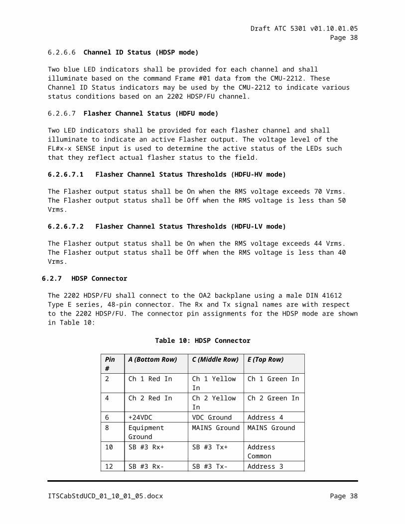
Draft ATC 5301 v01.10.01.05Page 38
6.3.5.14.2 Power Recovery
When the POWERDOWN input is high and the NRESET signal goes from low to high the CMU shall begin timing the programmed Minimum Flash Interval. During the Minimum Flash Interval, the CMU shall be in NFSA.
6.3.5.14.3 Power Up
Following initial application of AC+ Raw voltage, the CMU shall maintain a NFSA until the POWERDOWN input is high and the NRESET signal goes from low to high. The CMU shall then begin timing the programmed Minimum Flash Interval. During the Minimum Flash Interval, the CMU shall be in NFSA.
6.3.5.15 Minimum Flash Interval
The CMU shall be in NFSA during the Minimum Flash Interval. The Minimum Flash Interval shall be programmed in the serial memory key between the limits of 6 seconds to 16 seconds with an incremental adjustment of 1 second. The CMU shall not set a FSA during the Minimum Flash Interval.
6.3.5.16 Field Output Check
6.3.5.16.1 Field Check Fault
The CMU shall compare the active states of the field signals with the states reported by the ATC in the Type 81 or Type 67 frame. When a mismatch is detected for less than 700 milliseconds the CMU shall not cause a LFSA. When a mismatch is detected for 1000 milliseconds or more, the CMU shall cause a LFSA. When a mismatch is detected for more than 700 milliseconds but less than 1000 milliseconds, the CMU may or may not cause a LFSA. Field Output Check monitoring shall be disabled when the MAIN CONTACTOR COIL STATUS input is not active. There shall be a programming in the serial memory key to disable Field Output Check monitoring on a field input basis.
6.3.5.16.2 Field Check Status
The CMU shall compare the active states of the field signals with the states reported by the ATC in the Type 81 or Type 67 frame. When a mismatch is detected while a conflict, lack of signal, or multiple fault is timing, Field Check Status shall be reported with the fault to indicate the faulty channel(s) and color(s). Field Output Check monitoring shall be disabled when the MAIN CONTACTOR COIL STATUS input is not active. There shall be a programming in the serial memory key to disable Field Output Check monitoring on a field input basis.
6.3.5.17 CMU Temperature
The CMU shall measure the temperature at the CMU and report this value in the Type 182 frame. Temperature accuracy shall be +/-6 oC over the operating temperature range of the CMU.
6.3.6 Input Signals
There shall be a programming in the serial memory key to disable the Yellow input for each physical channel.
6.3.6.12212-HV Field Signal Voltage Inputs
For Lack of Signal monitoring (see 6.3.5.7) A Green or Yellow or Red signal input shall be sensed active when the reported voltage exceeds 70 Volts RMS and shall not be sensed active when it is less than 50 Volts RMS. A Green or Yellow or Red signal between 70 Volts RMS and 50 Volts RMS may or may not be sensed active.
ITSCabStdUCD_01_10_01_05.docx Page 38
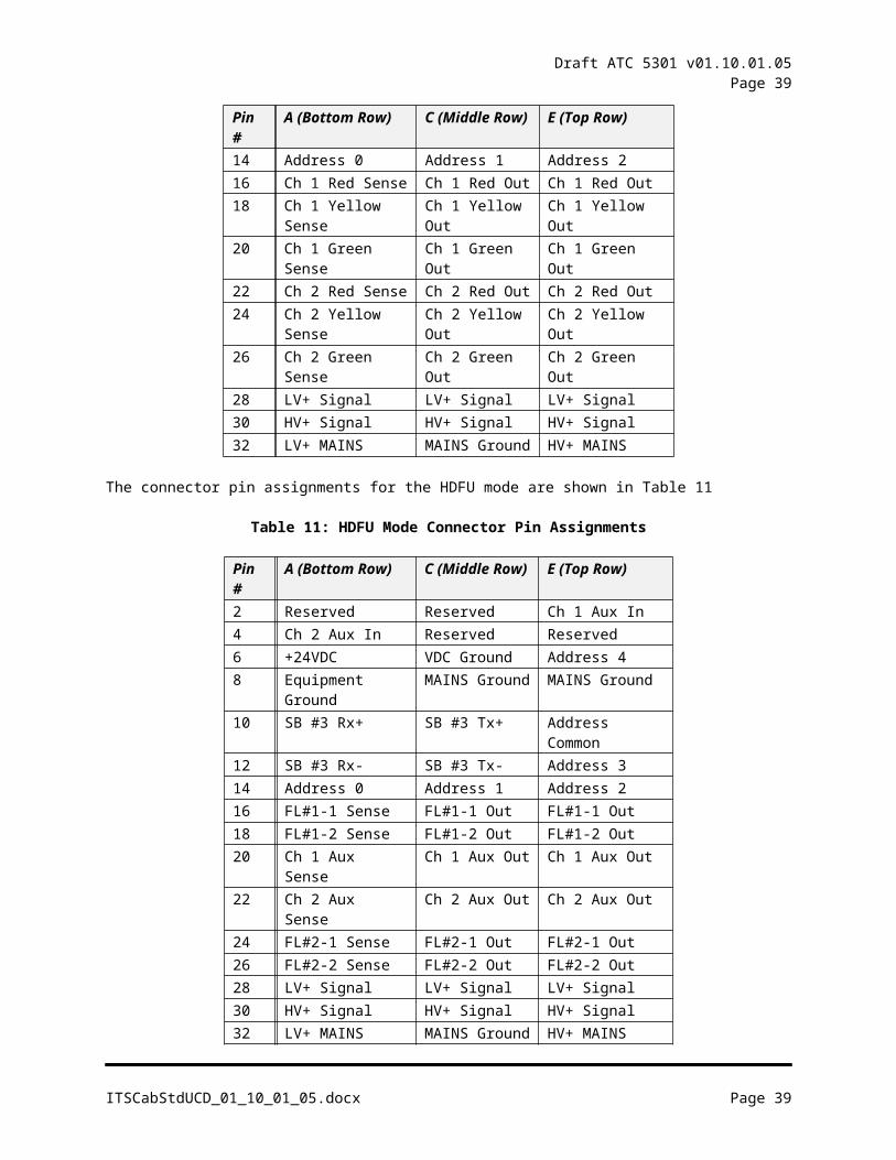
Draft ATC 5301 v01.10.01.05Page 39
For all other monitoring functions a Green or Yellow or Red signal input shall be sensed active when the reported voltage exceeds 25 Volts RMS and shall not be sensed active when it is less than 15 Volts RMS. A Green or Yellow or Red signal between 15 Volts RMS and 25 Volts RMS may or may not be sensed active.
6.3.6.22212-LV Field Signal Voltage Inputs
For Lack of Signal monitoring (see 6.3.5.7) A Green or Yellow or Red signal input shall be sensed active when the reported voltage exceeds 44 Volts RMS and shall not be sensed active when it is less than 40 Volts RMS. A Green or Yellow or Red signal between 44 Volts RMS and 40 Volts RMS may or may not be sensed active.
For all other monitoring functions a Green or Yellow or Red signal input shall be sensed active when the reported voltage exceeds 9 Volts RMS and shall not be sensed active when it is less than 6 Volts RMS. A Green or Yellow or Red signal between 9 Volts RMS and 6 Volts RMS may or may not be sensed active.
6.3.6.3Field Signal Load Current Outputs
A Green or Yellow or Red signal output shall be sensed active when the reported output load current exceeds the programmed threshold for that output and shall not be sensed active when the reported load current is less than the programmed threshold.
There shall be a programming in the serial memory key to disable Load Current monitoring on an output basis. There shall be a programming in the serial memory key to specify the Load Current Threshold on an output basis.
6.3.7 Control Signal Inputs
6.3.7.1Local Flash Status
The LF STATUS input shall be internally connected to the CMU Output Relay common pin. This input shall be considered active when the input voltage exceeds 43 Vdc. This input shall not be considered active when the input voltage is less than 39 Vdc. Signals between 43 Vdc and 39 Vdc may or may not be considered active. Operation of the cabinet in AUTO mode shall place 48 Vdc nominal on this input. Operation of the cabinet in FLASH mode shall be open circuit on this input. The CMU shall report the state of this input in the Type 209 frame.
6.3.7.2Main Contactor Coil Status
The MAIN CONTACTOR COIL STATUS input shall be connected to the Main Contactor signal bus relay coil. An active signal on this input indicates the signal bus should be powering the switch packs. This input shall be considered active when the input voltage exceeds 43 Vdc. This input shall not be considered active when the input voltage is less than 39 Vdc. Signals between 43 Vdc and 39 Vdc may or may not be considered active. The CMU shall report the state of this input in the Type 209 frame.
6.3.7.3Main Contactor Secondary Status
The MAIN CONTACTOR SECONDARY STATUS input shall be connected to the output side of the main contactor signal bus relay. The CMU shall report the state of this input in the Type 209 frame. For a 2212-HV CMU, this input shall be considered active when the input voltage exceeds 89 Volts RMS. This input shall not be considered active when the input voltage is less than 70 Volts RMS. For a 2212-LV CMU, this input shall be considered active when the input voltage exceeds 43 Volts RMS. This input shall not be considered active when the input voltage is less than 39 Volts RMS. Signals between 43 Volts RMS and 39 Volts RMS may or may not be considered active.
ITSCabStdUCD_01_10_01_05.docx Page 39
Draft ATC 5301 v01.10.01.05Page 40
6.3.7.4FTR Coil Drive Status
The FTR COIL DRIVE STATUS input shall be connected to the FTR COIL DRIVE signal in the AC SIGNAL POWER BUS. This input shall be considered active when the input voltage exceeds 43 Vdc. This input shall not be considered active when the input voltage is less than 39 Vdc. Signals between 43 Vdc and 39 Vdc may or may not be considered active. The CMU shall report the state of this input in the Type 209 frame.
6.3.7.5Circuit Breaker (CB) Trip Status
The CB TRIP STATUS input shall be connected to the auxiliary switch output of the circuit breaker unit. This input shall be considered active when the input voltage exceeds 43 Vdc. This input shall not be considered active when the input voltage is less than 39 Vdc. Signals between 43 Vdc and 39 Vdc may or may not be considered active. The CMU shall report the state of this input in the Type 209 frame.
6.3.7.6Front/Rear Door Switch
The CMU shall monitor the DOOR SWITCH FRONT and DOOR SWITCH REAR inputs. This input shall be considered active when the input voltage exceeds 14 Vdc. This input shall not be considered active when the input voltage is less than 10 Vdc. Signals between 14 Vdc and 10 Vdc may or may not be considered active. The CMU shall report the state of these inputs in the Type 209 frame.
6.3.7.7Monitor Interlock
The MONITOR INTERLOCK input shall be connected to VDC GROUND within the CMU.
6.3.7.8CMU Address Inputs
The address select input pins ADDRESS 0 and ADDRESS 1 define the Serial Bus #1 address of the CMU. The pins are left open for a logical False, and are connected to VDC GROUND for a logical True.
Table 12: CMU Address Inputs
ADDRESS 1
ADDRESS 0
SB #1 Address
False False 0x0FFalse True 0x10True False 0x11True True 0x12
6.3.8 Power and Circuit Requirements
6.3.8.1Mains Power
The 2212-HV CMU shall be operational over the voltage range of 80 Volts RMS to 135 Volts RMS. Surge current on AC+ Raw shall be less than 2 Amperes peak.
The 2212-LV CMU shall be operational over the voltage range of 35 Volts RMS to 60 Volts RMS. Surge current on AC+ Raw shall be less than 2 Amperes peak.
6.3.8.2+24VDC Power Supply
The CMU shall not use the Cabinet +24VDC Power Supply to run any of its internal circuitry. The +24 VDC MONITOR and +12 VDC MONITOR input circuits shall be optically isolated from the AC Mains
ITSCabStdUCD_01_10_01_05.docx Page 40
Draft ATC 5301 v01.10.01.05Page 41
circuitry. The maximum current into the +24 VDC or +12 VDC Monitor inputs over the voltage range of 0 VDC to 30 VDC shall be less than 20 milliamperes.
6.3.9 Failed State Output Circuit
The output relay of the CMU shall have one set of isolated Form C contacts. These relay contacts shall be rated for a minimum of three Amperes at 120 Volts RMS and 100,000 operations. Contact opening/closing time shall be 30 milliseconds or less. The relay coil shall be energized in the no fault state and de-energized in the FSA state.
6.3.10 Front Panel Indicators
All indicators shall be clear LEDs. Clear LEDs shall not depend on a reflector or diffusion as part of its design. Clear LEDs shall only show the die and not appear to be ON when exposed to ambient light. The following indicators shall be provided (Top to Bottom):
6.3.10.1 Power
A green POWER indicator shall illuminate to indicate AC Mains voltage is proper. It shall flash at a 2 Hertz rate when the NRESET or POWERDOWN input is low. For the 2212-HV CMU, it shall remain off when the voltage is less than 80 Volts RMS (+/-2 Volts RMS). For the 2212-LV CMU, it shall remain off when the voltage is less than 35 Volts RMS (+/-2 Volts RMS).
6.3.10.2 24 VDC Fail
A red 24VDC FAIL indicator shall illuminate when the CMU is in FSA as a result of a 24VDC cabinet power supply fault. The 24VDC FAIL indicator shall flash at a 2 Hertz rate when the 24 VDC monitor function is disabled.
6.3.10.3 12 VDC Fail
A red 12VDC FAIL indicator shall illuminate when the CMU is in FSA as a result of a 12VDC cabinet power supply fault.
6.3.10.4 Conflict
A red CONFLICT indicator shall illuminate when the CMU is in FSA as a result of a Conflicting channels fault.
6.3.10.5 Lack of Signal
A red LACK OF SIGNAL indicator shall illuminate when the CMU is in FSA as a result of a Lack of Signal Inputs fault.
6.3.10.6 Multiple
A red MULTIPLE indicator shall illuminate when the CMU is in FSA as a result of a Multiple Inputs fault.
6.3.10.7 CU/Local Flash
A red CU/LOCAL FLASH indicator shall illuminate when the CMU is in FSA as a result of a Type 62 – Send to Local Flash Command from the ATC, the LOCAL FLASH STATUS input sensed inactive, or CB TRIP STATUS active.
ITSCabStdUCD_01_10_01_05.docx Page 41

Draft ATC 5301 v01.10.01.05Page 42
6.3.10.8 Clearance
A red CLEARANCE indicator shall illuminate when the CMU is in FSA as a result of a Yellow Clearance or Yellow Plus Red Clearance fault.
6.3.10.9 Field Check
A red FIELD CHECK indicator shall illuminate when the CMU is in FSA as a result of a field output check fault. The indicator shall flash at a 2 Hertz rate when the CMU is in FSA with field check status as a result of Conflict, Lack of Signal, or Multiple fault.
6.3.10.10 SB #1 Error
A red SB #1 ERROR indicator shall illuminate when the CMU is in FSA as a result of a Serial Bus #1 fault.
6.3.10.11 SB #3 Error
A red SB #3 ERROR indicator shall illuminate when the CMU is in FSA as a result of a Serial Bus #3 fault.
6.3.10.12 Diagnostic
A red DIAGNOSTIC indicator shall illuminate when the CMU is in FSA as a result of a diagnostic fault. The DIAGNOSTIC indicator shall flash at a 4 Hertz rate if the serial memory key is not present and a FSA state does not exist (Front Door open).
6.3.10.13 SB #1 Rx
A yellow indicator shall pulse On each time the CMU correctly receives a frame on Serial Bus #1.
6.3.10.14 SB #3 Rx
A yellow indicator shall pulse On each time the CMU correctly receives a frame on Serial Bus #3.
ITSCabStdUCD_01_10_01_05.docx Page 42
Draft ATC 5301 v01.10.01.05Page 43
6.3.11 Mechanical
Figure 7: CMU Mechanical Details
ITSCabStdUCD_01_10_01_05.docx Page 43
Draft ATC 5301 v01.10.01.05Page 44
6.3.12 Serial Bus #3 Terminations
The Serial Bus #3 RxD+ input shall be terminated on the CMU to the Serial Bus #3 EIA-485 supply voltage through a 560 Ohm resistor. The Serial Bus #3 RxD- input shall be terminated on the CMU to Mains Ground through a 560 Ohm resistor. A 120 Ohm resistor shall be connected on the CMU between RxD+ and RxD-. The CMU Serial Bus #3 TxD drivers shall remain in the mark state with drivers enabled when the CMU is not transmitting a command frame.
Note: A 120 Ohm resistor shall be connected between Serial Bus #3 TxD+ and TxD- in the Auxiliary Display Unit (ADU) or on the Serial Bus #3 cable assembly in the last output assembly installed in the Serial Bus #3 daisy chain if an ADU is not installed.
6.3.13 Terminal Port
An Ethernet interface and connector shall be provided for interconnecting the CMU to a personal computer or network. The protocol for this Terminal Port is defined by the manufacturers.
6.3.13.1 Terminal Port Functions
The Ethernet port shall provide support for a static IP and DHCP Client at a minimum. A DHCP single address Server function option shall be provided to facilitate a direct connection to a PC. If a network DHCP Server is discovered on the network then this DHCP Server function shall be automatically disabled. The network settings of the Ethernet port shall be loaded directly from the serial memory key parameters if the download function is enabled.
6.3.13.2 Physical
The connector shall be mounted on the front panel and shall be an 8-position RJ-45 connector.
6.3.14 Serial Memory Key
The CMU shall have a Datakeytm model KC4210 Keycepticletm socket or equivalent serial memory key receptacle, which will intermate with the Datakeytm model LCK4000-RED, mounted on the front panel. The CMU shall be provided with a Datakeytm model LCK4000-RED serial memory key or equivalent. The serial memory key shall be rated for –40 to +80 degrees C operation.
Note: Datakeytm and Keycepticletm are registered trademarks of Datakey, Inc.
6.3.14.1 Monitor Unit Serial Memory Key Interface
The CMU shall not provide the capability to program the serial memory key. Writing to the serial memory key may be accomplished through the use of a serial memory key writer. The serial memory key shall be used by the CMU as a read only device. The 16 bit Frame Check Sequence (FCS) procedure defined in clause 4.5.2 of ISO/IEC 13239-2002(E) shall be used to verify the integrity of the read data. Failure to read the serial memory key correctly shall result in LFSA. Interface circuitry to the device shall utilize the LOFO switch on the serial memory key socket to ensure the device is removed and inserted with no power applied to the interface pins (i.e. dead socket).
6.3.14.2 Serial Memory Key Data
All bytes and bits marked as “reserved” shall be set to “0”.
Table 13 CMU Serial Memory Key Data
ITSCabStdUCD_01_10_01_05.docx Page 44
Draft ATC 5301 v01.10.01.05Page 45
Byte # Contents Description
1 0x20 Serial Memory Key Version (CMU 2212)2 Ch 1-9, …, 1-2 Permissive Programming for channels 1-32:
A bit set to “1” programs a channel pair to the permissive state. In the event the CMU has fewer than 32 channels, the bit positions corresponding to the nonexistent channels shall be 0.
Default programming shall be 0.
The Contents parameter contains on channel pair per bit position. For example, the contents of byte #5, “Ch 2-3, …, 1-26”, is as follows:
b0 = channel pair 1-26b1 = channel pair 1-27b2 = channel pair 1-28b3 = channel pair 1-29b4 = channel pair 1-30b5 = channel pair 1-31b6 = channel pair 1-32b7 = channel pair 2-3
If b1 is set, then channel 1 is permissive with channel 27.
3 Ch 1-17, …, 1-104 Ch 1-25, …, 1-185 Ch 2-3, …, 1-266 Ch 2-11, …, 2-47 Ch 2-19, …, 2-128 Ch 2-27, …, 2-209 Ch 3-6, …, 2-28
10 Ch 3-14, …, 3-711 Ch 3-22, …, 3-1512 Ch 3-30, …, 3-2313 Ch 4-10, …, 3-3114 Ch 4-18, …, 4-1115 Ch 4-26, …, 4-1916 Ch 5-7, …, 4-2717 Ch 5-15, …, 5-818 Ch 5-23, …, 5-1619 Ch 5-31, …, 5-2420 Ch 6-13, …, 5-3221 Ch 6-21, …, 6-1422 Ch 6-29, …, 6-2223 Ch 7-12, …, 6-3024 Ch 7-20, …, 7-1325 Ch 7-28, …, 7-2126 Ch 8-12, …, 7-2927 Ch 8-20, …, 8-1328 Ch 8-28, …, 8-2129 Ch 9-13, …, 8-2930 Ch 9-21, …, 9-1431 Ch 9-29, …, 9-2232 Ch 10-15, …, 9-3033 Ch 10-23, …, 10-1634 Ch 10-31, …, 10-2435 Ch 11-18, …, 10-3236 Ch 11-26, …, 11-1937 Ch 12-14, …, 11-2738 Ch 12-22, …, 12-1539 Ch 12-30, …, 12-2340 Ch 13-19, …, 12-3141 Ch 13-27, …, 13-2042 Ch 14-17, …, 13-2843 Ch 14-25, …, 14-1844 Ch 15-16, …, 14-2645 Ch 15-24, …, 15-17
ITSCabStdUCD_01_10_01_05.docx Page 45
Draft ATC 5301 v01.10.01.05Page 46
Byte # Contents Description
46 Ch 15-32, …, 15-2547 Ch 16-24, …, 16-1748 Ch 16-32, …, 16-2549 Ch 17-25, …, 17-1850 Ch 18-19, …, 17-2651 Ch 18-27, …, 18-2052 Ch 19-22, …, 18-2853 Ch 19-30, …, 19-2354 Ch 20-26, …, 19-3155 Ch 21-23, …, 20-2756 Ch 21-31, …, 21-2457 Ch 22-29, …, 21-3258 Ch 23-28, …, 22-3059 Ch 24-28, …, 23-2960 Ch 25-29, …, 24-2961 Ch 26-31, …, 25-3062 Ch 28-30, …, 26-3263 Ch 31-32, …, 28-3164 Ch 8:1 Lack of Signal Input Enable:
A bit set to “1” enables the Lack of Signal Input monitoring function for that channel. This bit shall be set to “0” for any channel that has an input mapped to a virtual channel. In the event the CMU has fewer than 32 channels, the bit positions corresponding to the nonexistent channels shall be 0. Default programming shall be 1.
65 Ch 16:966 Ch 24:17
67 Ch 32:18
68 Ch 8:1 Dark Channel Map #1A bit set to “1” disables the Lack of Signal Input monitoring function for that channel. For channels that are set to 0, Lack of Signal Input Enable programming shall determine Lack of Signal Input operation. Default programming shall be 0.
69 Ch 16:970 Ch 24:17
71 Ch 32:18
72 Ch 8:1 Dark Channel Map #2A bit set to “1” disables the Lack of Signal Input monitoring function for that channel. For channels that are set to 0, Lack of Signal Input Enable programming shall determine Lack of Signal Input operation. Default programming shall be 0.
73 Ch 16:974 Ch 24:17
75 Ch 32:18
76 Ch 8:1 Dark Channel Map #3A bit set to “1” disables the Lack of Signal Input monitoring function for that channel. For channels that are set to 0, Lack of Signal Input Enable programming shall determine Lack of
77 Ch 16:978 Ch 24:1779 Ch 32:18
ITSCabStdUCD_01_10_01_05.docx Page 46
Draft ATC 5301 v01.10.01.05Page 47
Byte # Contents Description
Signal Input operation. Default programming shall be 0.80 Ch 8:1 Dark Channel Map #4A bit set to “1” disables the Lack of Signal Input monitoring function for that channel. For channels that are set to 0, Lack of Signal Input Enable programming shall determine Lack of Signal Input operation. Default programming shall be 0.
81 Ch 16:982 Ch 24:17
83 Ch 32:18
84 Ch 8:1 GY Multiple Channel Enable:A bit set to “1” enables the Green/Yellow Multiple Channel monitoring function for that channel. This bit shall be set to “0” for any channel that has had a Green or Yellow input remapped to a virtual channel. In the event the CMU has fewer than 32 channels, the bit positions corresponding to the nonexistent channels shall be 0. Default programming shall be 1.
85 Ch 16:986 Ch 24:17
87 Ch 32:18
88 Ch 8:1 YR Multiple Channel Enable:A bit set to “1” enables the Yellow/Red Multiple Channel monitoring function for that channel. This bit shall be set to “0” for any channel that has had a Yellow or Red input remapped to a virtual channel. In the event the CMU has fewer than 32 channels, the bit positions corresponding to the nonexistent channels shall be 0. Default programming shall be 1.
89 Ch 16:990 Ch 24:17
91 Ch 32:18
92 Ch 8:1 GR Multiple Channel Enable:A bit set to “1” enables the Green/Red Multiple Channel monitoring function for that channel. This bit shall be set to “0” for any channel that has had a Green or Red input remapped to a virtual channel. In the event the CMU has fewer than 32 channels, the bit positions corresponding to the nonexistent channels shall be 0. Default programming shall be 1.
93 Ch 16:994 Ch 24:17
95 Ch 32:18
96 Ch 8:1 Minimum Yellow Change Enable:A bit set to “1” enables the Minimum Yellow Change monitoring function for that channel. In the event the CMU has fewer than 32 channels, the bit positions corresponding to the nonexistent channels shall be 0. Default programming shall be 1.
97 Ch 16:998 Ch 24:17
99 Ch 32:18
100 Ch 8:1 Minimum Yellow Change Plus Red Clearance Enable:A bit set to “1” enables the Minimum Yellow Change Plus Red monitoring function for that
101 Ch 16:9102 Ch 24:17
ITSCabStdUCD_01_10_01_05.docx Page 47
Draft ATC 5301 v01.10.01.05Page 48
Byte # Contents Description
channel. In the event the CMU has fewer than 32 channels, the bit positions corresponding to the nonexistent channels shall be 0. Default
103 Ch 32:18
104 Ch 8:1 Yellow Input Disable:A bit set to “1” forces the Yellow input to the OFF state for that channel. In the event the CMU has fewer than 32 physical channels, the bit positions corresponding to the nonexistent channels shall be 0. Default programming shall be 0.
105 Ch 16:9106 Ch 24:17
107 Ch 32:25
108 Ch 8:1 Output Current Sense Enable Red:A bit set to “1” enables the Lack of Signal current monitoring function for the Red Output of the channel. This bit shall be set to “0” for any Red input that has been mapped to a virtual channel. In the event the CMU has fewer than 32 physical channels, the bit positions corresponding to the nonexistent channels shall be 0. Default programming shall be 1.
109 Ch 16:9110 Ch 24:17
111 Ch 32:25
112 Ch 8:1 Output Current Sense Enable Yellow:A bit set to “1” enables the Lack of Signal current monitoring function for the Yellow Output of the channel. This bit shall be set to “0” for any Yellow input that has been mapped to a virtual channel. In the event the CMU has fewer than 32 physical channels, the bit positions corresponding to the nonexistent channels shall be 0. Default programming shall be 1.
113 Ch 16:9114 Ch 24:17
115 Ch 32:25
116 Ch 8:1 Output Current Sense Enable Green:A bit set to “1” enables the Lack of Signal current monitoring function for the Green Output of the channel. This bit shall be set to “0” for any Green input that has been mapped to a virtual channel. In the event the CMU has fewer than 32 physical channels, the bit positions corresponding to the nonexistent channels shall be 0. Default programming shall be 1.
117 Ch 16:9118 Ch 24:17
119 Ch 32:25
120 Channel 1 Red Output Current Sense ThresholdThe threshold value for Red current sense shall be programmed in scaled milliamps. IF Param >120
Then Current = (Param *16) – 1800Else Current = Param
If Param > 250 Then Current = “> 2200” mA
121 Channel 2 122 Channel 3 123 Channel 4 124 Channel 5 125 Channel 6 126 Channel 7 127 Channel 8 128 Channel 9
ITSCabStdUCD_01_10_01_05.docx Page 48
Draft ATC 5301 v01.10.01.05Page 49
Byte # Contents Description
129 Channel 10 130 Channel 11 131 Channel 12 132 Channel 13 133 Channel 14 134 Channel 15 135 Channel 16 136 Channel 17 137 Channel 18 138 Channel 19 139 Channel 20 140 Channel 21 141 Channel 22 142 Channel 23 143 Channel 24 144 Channel 25145 Channel 26146 Channel 27147 Channel 28148 Channel 29149 Channel 30150 Channel 31151 Channel 32152 Channel 1 Yellow Output Current Sense Threshold
The threshold value for Yellow current sense shall be programmed in scaled milliamps. IF Param >120
Then Current = (Param *16) – 1800Else Current = Param
If Param > 250 Then Current = “> 2200” mA
153 Channel 2 154 Channel 3 155 Channel 4 156 Channel 5 157 Channel 6 158 Channel 7 159 Channel 8 160 Channel 9 161 Channel 10 162 Channel 11 163 Channel 12 164 Channel 13 165 Channel 14 166 Channel 15 167 Channel 16 168 Channel 17 169 Channel 18 170 Channel 19 171 Channel 20 172 Channel 21 173 Channel 22
ITSCabStdUCD_01_10_01_05.docx Page 49
Draft ATC 5301 v01.10.01.05Page 50
Byte # Contents Description
174 Channel 23 175 Channel 24 176 Channel 25177 Channel 26178 Channel 27179 Channel 28180 Channel 29181 Channel 30182 Channel 31183 Channel 32184 Channel 1 Green Output Current Sense Threshold
The threshold value for Green current sense shall be programmed in scaled milliamps. IF Param >120
Then Current = (Param *16) – 1800Else Current = Param
If Param > 250 Then Current = “> 2200” mA
185 Channel 2 186 Channel 3 187 Channel 4 188 Channel 5 189 Channel 6 190 Channel 7 191 Channel 8 192 Channel 9 193 Channel 10 194 Channel 11 195 Channel 12 196 Channel 13 197 Channel 14 198 Channel 15 199 Channel 16 200 Channel 17 201 Channel 18 202 Channel 19 203 Channel 20 204 Channel 21 205 Channel 22 206 Channel 23 207 Channel 24 208 Channel 25209 Channel 26210 Channel 27211 Channel 28212 Channel 29213 Channel 30214 Channel 31215 Channel 32216 Red Ch 8:1 Field Output Check Enable:
A bit set to “1” enables the Field Output Check monitoring function for that input. This bit shall
217 Red Ch 16:9218 Red Ch 24:17
ITSCabStdUCD_01_10_01_05.docx Page 50
Draft ATC 5301 v01.10.01.05Page 51
Byte # Contents Description
be set to “0” for any input that has been remapped to a virtual channel. In the event the CMU has fewer than 32 channels, the bit positions corresponding to the nonexistent inputs shall be 0. Default programming shall be 1.
219 Red Ch 32:25220 Yellow Ch 8:1221 Yellow Ch 16:9222 Yellow Ch 24:17223 Yellow Ch 32:25224 Green Ch 8:1225 Green Ch 16:9226 Green Ch 24:17227 Green Ch 32:25
228 Minimum Flash Time
Minimum Flash TimeValues of 0 thru 5 shall result in 6 seconds of minimum flash. Maximum value is 15. Default programming shall be 6.
229 Misc Control
Misc Controlb0 = Set to 1 shall enable the +12 VDC Power
Supply monitor.b1 = Set to 1 shall enable HDFU #2b2:b7 = Reserved
Default programming shall be 0x01.230 Ch 29 Red Virtual Channel Assignment
Channels that have not been assigned shall be set to 0. Default programming shall be 0.
Bits 4:0 specify the physical channel number (1 to 28)Bits 6:5 specify the physical input
01 = Red10 = Yellow11 = Green
Bit 7 = reserved
231 Ch 29 Yellow232 Ch 29 Green233 Ch 30 Red234 Ch 30 Yellow235 Ch 30 Green236 Ch 31 Red237 Ch 31 Yellow238 Ch 31 Green239 Ch 32 Red240 Ch 32 Yellow241 Ch 32 Green242 Ch 8:1 HDSP Channel Enable
A bit set to “1” enables the channel monitoring function of the HDSP. This bit shall be set to “0” for any channel that has been disabled or is not installed. Default programming shall be 1.
243 Ch 16:9244 Ch 24:17
245 Ch 32:25
246:285 ASCII string
Monitor IDA packed 40 character ID shall be stored in ASCII format. Allowable characters are 020h through 07Eh. If less than 40 characters are used, the unused locations shall be set to 00h. Default programming shall be 00h.
286:325 ASCII string
User IDA packed 40 character ID shall be stored in ASCII format. Allowable characters are 020h through 07Eh. If less than 40 characters are
ITSCabStdUCD_01_10_01_05.docx Page 51
Draft ATC 5301 v01.10.01.05Page 52
Byte # Contents Description
used, the unused locations shall be set to 00h. Default programming shall be 00h.
326 0x00
Ethernet Controlb0: 1=DHCP Client Enableb1: 1=DHCP Server Enable (if provided)b2:b6 Reservedb7: 1=Enable download from datakey
327 LS octet Ethernet IP Address328 octet329 octet330 MS octet331 LS octet Ethernet Subnet Mask332 octet333 octet334 MS octet335 LS octet Ethernet Gateway Address336 octet337 octet338 MS octet339 Ascii byte #1 Ethernet Host Name (ascii)
A computer name can be up to 15 alphanumeric characters with no blank spaces. The name must be unique on the network and can contain the following characters:
0-9, A-Z, _, -
Unused characters shall be set to 0x00.
340 Ascii byte #2341 Ascii byte #3342 Ascii byte #4343 Ascii byte #5344 Ascii byte #6345 Ascii byte #7346 Ascii byte #8347 Ascii byte #9348 Ascii byte #10349 Ascii byte #11350 Ascii byte #12351 Ascii byte #13352 Ascii byte #14353 Ascii byte #15354 FYA Pair #1 FYA OLP Parameters
b4:b0 = OLP Channel number - 1b5 = Channel Enableb6 = Flash Rate Detectb7 = Reserved
355 FYA Pair #2356 FYA Pair #3357 FYA Pair #4358 FYA Pair #5359 FYA Pair #6360 FYA Pair #1 FYA LT Parameters
b4:b0 = Green Arrow Channel numberb5 = Reservedb6 = R&Y Input Enableb7 = Reserved
361 FYA Pair #2362 FYA Pair #3363 FYA Pair #4364 FYA Pair #5
ITSCabStdUCD_01_10_01_05.docx Page 52

Draft ATC 5301 v01.10.01.05Page 53
Byte # Contents Description
365 FYA Pair #6366 FYA Pair #1 FYA OPP Parameters
b4:b0 = Opposing Thru Channel numberb5 = Reservedb6 = Reservedb7 = Reserved
367 FYA Pair #2368 FYA Pair #3369 FYA Pair #4370 FYA Pair #5371 FYA Pair #6
372 0, 1:130
App Specific Buffer Size Decimal byte count of the App Specific Buffer including the Mfg ID. This buffer (if used) shall extend from offset 510 down to the Reserved limit of 373. The first (lowest) two bytes of the buffer shall be the NEMA Mfg ID number.
373:510 0x00 Reserved for future use or App Specific buffer. 511 FCS lsb 16 bit Check Value
FCS Polynomial calculation of bytes #1 through #510. 512 FCS lsb
6.3.15Serial Memory Key Application Specific BufferA section shall be reserved for CMU parameters that are defined by the CMU manufacturer for application specific functionality outside of this standard. This section shall begin at a Data Key location specified by “511 - App Specific Buffer Size” and end at byte 510. If this section is not used by the CMU, then the App Specific Buffer Size parameter shall be set to zero. The first (lowest) two bytes of this buffer shall be the NEMA Manufacturer Specific ID. The manufacturer specific code is a 16 bit binary number. These codes are maintained and issued by NEMA.
The intention in placing manufacturer specific codes in the Data Key parameter buffer that are reserved for manufacturers use is to allow equipment to differentiate between Data Keys that may contain the same data. (Authorized Engineering Information.)
6.3.16 CMU Connector
The CMU connector shall be a DIN 4161264 Header Type.
6.3.16.1 CMU Pin Assignments
Signal names are with respect to the CMU.
Table 14: CMU Connector Pin Assignments
Pin # Function Pin # FunctionA1 +24VDC Monitor B1 ReservedA2 +12VDC Monitor B2 External Test ResetA3 VDC Ground B3 Serial Bus #1 DisableA4 Monitor Interlock B4 ReservedA5 Address 0 B5 Address 1A6 Reserved B6 ReservedA7 SB1 TxData + B7 SB1 TxData -
ITSCabStdUCD_01_10_01_05.docx Page 53
Draft ATC 5301 v01.10.01.05Page 54
Pin # Function Pin # FunctionA8 SB1 RxData + B8 SB1 RxData -A9 SB1 TxClock + B9 SB1 TxClock -
A10 SB1 RxClock + B10 SB1 RxClock -A11 Reserved B11 ReservedA12 Reserved B12 ReservedA13 Reserved B13 ReservedA14 Reserved B14 ReservedA15 Line Sync + B15 Line Sync -A16 Nreset + B16 Nreset -A17 PowerDown + B17 PowerDown -A18 SB3 TxData + B18 SB3 TxData -A19 SB3 RxData + B19 SB3 RxData -A20 SB3 Clock+ B20 SB3 Clock-A21 LF Status B21 LF StatusA22 Output Relay NO B22 Output Relay NOA23 CB Trip Status B23 ReservedA24 MC Coil Status B24 ReservedA25 MC Secondary Status B25 ReservedA26 FTR Coil Drive Status B26 ReservedA27 Door Switch Front B27 ReservedA28 Door Switch Rear B28 ReservedA29 Reserved B29 ReservedA30 Reserved B30 MAINS PowerA31 Equipment Ground B31 ReservedA32 Reserved B32 MAINS Ground (Neutral)Note: Output Relay NO is open during FSA (de-energized).
6.4 Cabinet Power Supply Requirements, High Voltage Versions
Standardization LevelDescription Controlled by Standard?
Interface Signal Names and Electrical Characteristics YesConnector Type and Pin Assignments YesMechanical Dimensions Yes
Section 6.4 describes the requirements for two basic power supplies with different from factors and ratings. Because the interface between the cabinet assemblies and power supply is not controlled by this standard, it is not a conformance requirement that these power supplies be used in an ATC cabinet. Other power supplies may be substituted that meet or exceed the requirements stated below.
6.4.1 Model 2216-HV Cabinet Power Supply
6.4.1.1General
The model 2216 Cabinet Power Supply is a modular 19 inch rack mounted power supply device providing the DC voltages necessary for operating the ATC Cabinet in the HV mode.
ITSCabStdUCD_01_10_01_05.docx Page 54
Draft ATC 5301 v01.10.01.05Page 55
The model 2216-24-HV provides a regulated 24VDC output and a regulated 48 Vdc output. The model 2216-2412-HV model provides a regulated 24 Vdc output, a regulated 48 Vdc output, and a regulated 12 Vdc output option for powering the Input Assembly devices. Power Factor Correction shall be provided. Unless otherwise specified, all model 2216 requirements apply to both model types.
The model 2217 Cabinet Power Supply is a card mounted power supply device providing the DC voltages necessary for operating the ATC Cabinet in the HV mode. The model 2217 provides a regulated 24VDC output and a regulated 48 Vdc output. Power Factor Correction shall be provided.
6.4.1.2Mechanical
The model 2216 shall be 1U (1.7”) in height maximum and designed to mount into a 19 inch EIA rack. The maximum depth of the model 2216 shall be less than 8.0”.
6.4.1.3Inputs
The model 2216 shall be powered from AC Line provided by an AC Line cord with NEMA Type 515 plug. The input voltage range shall be 80 to 270 Vac, 45 to 65 Hz. Power Factor Correction shall be greater than 0.95.
6.4.1.3.1Input Surge
The AC Line input surge at power-up shall be less than 20 Amps maximum at rated full load.
6.4.1.4Outputs
6.4.1.4.1Model 2216-24
The model 2216-24 shall provide: 48 Vdc +/- 2 Vdc at 1 Amp maximum 24 Vdc +/- 2 Vdc at 5 Amps maximum
Each DC output shall be electrically isolated from AC Mains, Earth Ground, and other DC outputs. Fans shall not be used for cooling.
6.4.1.4.2Model 2216-2412
The model 2216-2412 shall provide: 48 Vdc +/- 2 Vdc at 1 Amp maximum 24 Vdc +/- 2 Vdc at 4 Amps maximum 12 Vdc +/- 1 Vdc at 5 Amps maximum
Each DC output shall be electrically isolated from AC Mains and Earth Ground. The 24 Vdc and 12 Vdc outputs share a common ground. Fans shall not be used for cooling..
6.4.1.4.3 DC Output Ripple
The DC Output Ripple on each output shall be less than 300 mVpp when measured at 20MHz of bandwidth using a 12" twisted pair-wire terminated with a 0.1uf & 47uf capacitor.
6.4.1.4.4 DC Start-up Time
The DC outputs shall attain regulated output levels within 1000 milliseconds of applied AC Line voltage of 110 Vac nominal across the operating temperature range and at rated full load.
ITSCabStdUCD_01_10_01_05.docx Page 55
Draft ATC 5301 v01.10.01.05Page 56
6.4.1.4.5 DC Hold-up Time
The DC outputs shall maintain regulated output level for a minimum of 50 milliseconds across the operating temperature range and at rated full load.
6.4.1.5Front Panel Indicators
All indicators shall be clear LEDs. Clear LEDs shall not depend on a reflector or diffusion as part of its design. Clear LEDs shall not appear to be ON when exposed to ambient light. The following indicators shall be provided:
6.4.1.5.1AC Line
A green AC Line indicator shall illuminate to indicate Operational input voltage is proper and the AC Line fuse is intact.
6.4.1.5.248 VDC
A green indicator shall illuminate to indicate the 48 VDC output is active and the fuse is intact.
6.4.1.5.324 VDC
A green indicator shall illuminate to indicate the 24 VDC output is active and the fuse is intact.
6.4.1.5.412 VDC (model 2216-2412 Only)
A green indicator shall illuminate to indicate the 12 VDC output is active and the fuse is intact.
6.4.1.6DC Voltage Test Jacks
Banana style test jacks shall be provided on the front panel for each DC output and DC ground. Mating banana plug spring width shall be 0.175 inches nominal.
6.4.1.7DC Output Connector
The output connector is a Phoenix Contact #1825161 and mates with a Phoenix Contact #1825352 or equivalent. Pin #1 is the right most pin when viewed from the rear of the supply. See Table 15.
Table 15: Power Supply DC Output Connector
Pin Function1 +48VDC2 48VDC Ground**
3 +24VDC4 +12VDC (PS-2216-2412 only)5 24/12 VDC Ground6 Chassis Ground
**Note that the 48 VDC output shall be electrically isolated from the AC Line input and the 24VDC and 12 VDC outputs. The 48VDC Ground (pin #2) shall be connected within the cabinet to the same AC Neutral that the Cabinet Monitor Unit (CMU) is connected to.
ITSCabStdUCD_01_10_01_05.docx Page 56

Draft ATC 5301 v01.10.01.05Page 57
6.4.2 Model 2217-HV Cabinet Power Supply
6.4.2.1General
The model 2217 Cabinet Power Supply is a card mounted power supply device providing the DC voltages necessary for operating the ATC Cabinet in the HV mode. The model 2217 provides a regulated 24VDC output and a regulated 48 Vdc output. Power Factor Correction shall be provided.
6.4.2.2Inputs
The model 2217 shall be powered from AC Line. The input voltage range shall be 80 to 270 Vac, 45 to 65 Hz. Power Factor Correction shall be greater than 0.95.
6.4.2.2.1Input Surge
The AC Line input surge at power-up shall be less than 20 Amps maximum at rated full load.
6.4.2.3Outputs
The model 2217 shall provide: 48 Vdc +/- 2 Vdc at 1 Amp maximum 24 Vdc +/- 2 Vdc at 3 Amps maximum
Each DC output shall be electrically isolated from AC Mains, Earth Ground, and other DC outputs. Fans shall not be used for cooling.
6.4.2.3.1 DC Output Ripple
The DC Output Ripple on each output shall be less than 300 mVpp when measured at 20MHz of bandwidth using a 12" twisted pair-wire terminated with a 0.1uf & 47uf capacitor.
6.4.2.3.2 DC Start-up Time
The DC outputs shall attain regulated output levels within 1000 milliseconds of applied AC Line voltage of 110 Vac nominal across the operating temperature range and at rated full load.
6.4.2.3.3 DC Hold-up Time
The DC outputs shall maintain regulated output level for a minimum of 50 milliseconds across the operating temperature range and at rated full load.
6.4.2.4Front Panel Indicators
All indicators shall be clear LEDs. Clear LEDs shall not depend on a reflector or diffusion as part of its design. Clear LEDs shall not appear to be ON when exposed to ambient light. The following indicators shall be provided:
6.4.2.4.1AC Line
A green AC Line indicator shall illuminate to indicate Operational input voltage is proper and the AC Line fuse is intact.
6.4.2.4.248 VDC
A green indicator shall illuminate to indicate the 48 VDC output is active and the fuse is intact.
ITSCabStdUCD_01_10_01_05.docx Page 57
Draft ATC 5301 v01.10.01.05Page 58
6.4.2.4.324 VDC
A green indicator shall illuminate to indicate the 24 VDC output is active and the fuse is intact.
6.4.2.5Mechanical
Figure 8: Model 2217 Mechanical Details
6.4.2.5.1DC Output Connector
The connector on the model 2217 shall a Phoenix #1776553 or equivalent. The mating connector on the rack is a Phoenix #1785997 or equivalent. Pin #1 is the right most pin when viewed from the rear of the supply. See Error: Reference source not found.
Table 16: Model 2217 Power Supply DC Output Connector
Pin Function1 Chassis Ground2 AC- Neutral3 AC+ Power 4 24VDC Ground 5 +24VDC Output6 48VDC Ground**7 +48VDC Output
**Note that the 48 VDC output shall be electrically isolated from the AC Line input and the 24VDC output. The 48VDC Ground (pin #6) shall be connected within the cabinet to the same MAINS GROUND that the Cabinet Monitor Unit (CMU) is connected to.
ITSCabStdUCD_01_10_01_05.docx Page 58
Draft ATC 5301 v01.10.01.05Page 59
6.5 Cabinet Power Supply Requirements, Low Voltage Version
Standardization LevelDescription Controlled by Standard?
Interface Signal Names and Electrical Characteristics YesConnector Type and Pin Assignments YesMechanical Dimensions Yes
Section 6.5 describes the requirements for two basic power supplies with different from factors and ratings. Because the interface between the cabinet assemblies and power supply is not controlled by this standard, it is not a conformance requirement that these power supplies be used in an ATC cabinet. Other power supplies may be substituted that meet or exceed the requirements stated below.
6.5.1 Model 2248 Cabinet Power Supply
6.5.1.1General
The model 2248 Cabinet Power Supply is a modular 19 inch rack mounted power supply device providing the DC voltages necessary for operating the ATC Low Voltage (LV) Cabinet. The model 2248 provides a regulated 24Vdc output and a regulated 48 Vdc output, and is intended to provide 48 Vdc power to the Output Assembly components and DC based signal lamps.
6.5.1.2Mechanical
The model 2248 shall be 1U (1.7”) in height maximum and designed to mount into a 19 inch EIA rack. The maximum depth of the model 2248 shall be less than 8.0”.
6.5.1.3Inputs
The model 2248 shall be powered from AC Line provided by an AC Line cord with NEMA Type 515 plug. The input voltage range shall be 80 to 270 Vac, 45 to 65 Hz. Power Factor Correction shall be greater than 0.95.
6.5.1.3.1 Input Surge
The AC Line input surge at power-up shall be less than 50 Amps maximum at rated full load.
6.5.1.4Outputs
The model 2248 shall provide: 48 Vdc +/- 2 Vdc at 6 Amp maximum 24 Vdc +/- 2 Vdc at 4 Amps maximum
Each DC output shall be electrically isolated from AC Mains, Earth Ground, and other DC outputs. Fans shall not be used for cooling.
6.5.1.4.1 DC Output Ripple
The DC Output Ripple on each output shall be less than 500 mVpp when measured at 20MHz of bandwidth using a 12" twisted pair-wire terminated with a 0.1uf & 47uf capacitor.
6.5.1.4.2 DC Start-up Time
The DC outputs shall attain regulated output levels within 1000 milliseconds of applied AC Line voltage of 110 Vac nominal across the operating temperature range and at rated full load.
ITSCabStdUCD_01_10_01_05.docx Page 59
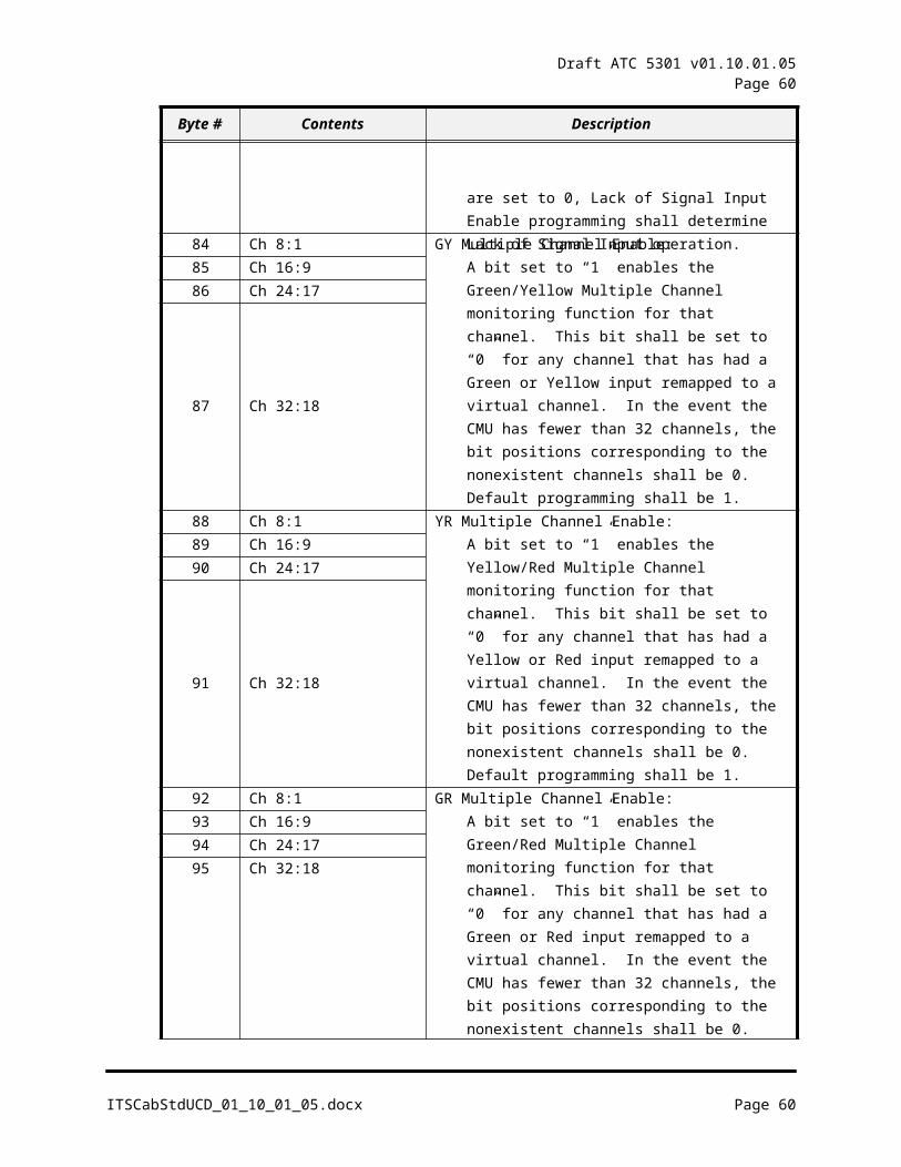
Draft ATC 5301 v01.10.01.05Page 60
6.5.1.4.3 DC Hold-up Time
The DC outputs shall maintain regulated output level for a minimum of 50 milliseconds across the operating temperature range and at rated full load.
6.5.1.5Front Panel Indicators
All indicators shall be clear LEDs. Clear LEDs shall not depend on a reflector or diffusion as part of its design. Clear LEDs shall not appear to be ON when exposed to ambient light. The following indicators shall be provided:
6.5.1.5.1AC Line
A green AC Line indicator shall illuminate to indicate Operational input voltage is proper and the AC Line fuse is intact.
6.5.1.5.248 VDC
A green indicator shall illuminate to indicate the 48 VDC output is active and the fuse is intact.
6.5.1.5.324 VDC
A green indicator shall illuminate to indicate the 24 VDC output is active and the fuse is intact.
6.5.1.6DC Voltage Test Jacks
Banana style test jacks shall be provided on the front panel for each DC output and DC ground. Mating banana plug spring width shall be 0.175 inches nominal.
6.5.1.7DC Output Connector
The output connector is a Phoenix Contact #1825161 and mates with a Phoenix Contact #1825352 or equivalent. Pin #1 is the right most pin when viewed from the rear of the supply. See Table 18.
Table 17: Power Supply DC Output Connector
Pin Function1 +48VDC2 48VDC Ground**
3 +24VDC4 Reserved5 24VDC Ground6 Chassis Ground
**Note that the 48 VDC output shall be electrically isolated from the AC Line input and the 24VDC output. The 48VDC Ground (pin #2) shall be connected within the cabinet to the same AC Neutral that the Cabinet Monitor Unit (CMU) is connected to.
ITSCabStdUCD_01_10_01_05.docx Page 60
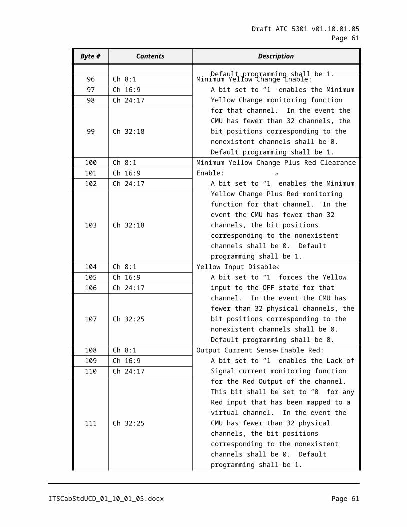
Draft ATC 5301 v01.10.01.05Page 61
6.6 Model 2220 Auxiliary Display Unit
Standardization LevelDescription Controlled by Standard?
Interface Signal Names and Electrical Characteristics YesConnector Type and Pin Assignments NoMechanical Dimensions No
6.6.1 General
The Model 2220 Auxiliary Display Unit (ADU) is a modular display that provides an enhanced user interface for the ATC Cabinet Monitor Unit system. The Auxiliary Display Unit mounts into a 1U space of the EIA 19 inch rack of the cabinet. The model 2220 shall not be required in the cabinet for the CMU22212 to operate normally.
The model 2220 provides a display function in a modular fashion for the installed cabinet monitor unit and utilizes an LED based channel output status display and a menu driven LCD display to view status, configuration, and logs. Five buttons are included to navigate the menu system. The CMU communicates to the model 2220 via Serial Bus #3.
Guidance: The Auxillary Display unit is an optional assembly for the ATC Cabinet. Mechanical dimensions as well as connector type and pin assignments are not controlled by the standard. The following section, defining the Model 2220 Auxillary Display Unit, is one example of how the user interface for the Cabinet Monitor Unit can be realized.
The display data shall be created and formatted by the installed CMU2212.
6.6.2 Mechanical
The model 2220 shall be 1U (1.7”) in height maximum and designed to mount into a 19 inch EIA rack. The maximum depth of the model 2220 shall be less than 3.0”.
6.6.2.1Power Connector
The 48VDC power is supplied with a Phoenix Contact 3-pin header 1776511, with a mating harness plug part number 1777992. Pin #1 is the rightmost pin when viewed from the connector end (back side of the ADU).
Table 18: ADU Power Connector Signals
Pin Function1 +48VDC2 48VDC Ground**3 Earth Ground
**The 48VDC Ground (pin #2) must be connected within the cabinet to the same MAINS GROUND of the Cabinet Monitor Unit (CMU).
6.6.2.2SB#3 Connector
This port provides the EIA-485 data path to the CMU Cabinet Monitor Unit (CMU) using Serial Bus #3. A standard CAT-5 network cable with RJ-45 connector shall be used. The signals shall be MAINS GROUND referenced, which is the same Ground point as the CMU2212. Signal names are with respect to the model 2220.
ITSCabStdUCD_01_10_01_05.docx Page 61
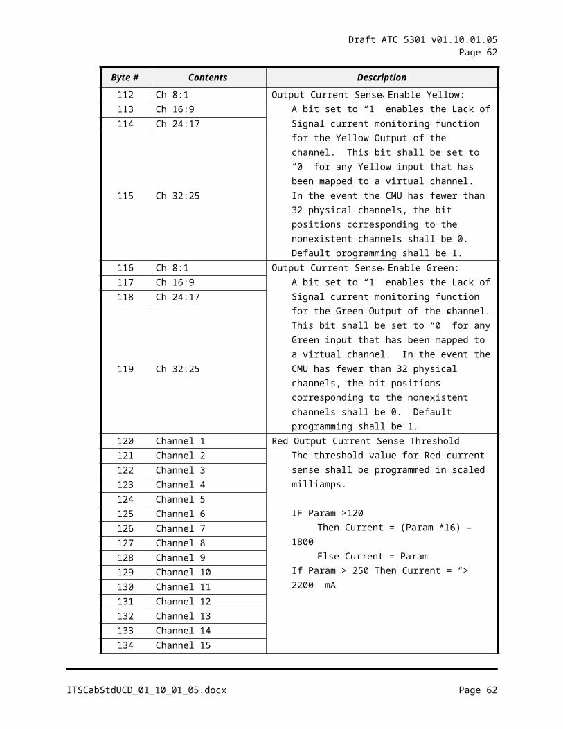
Draft ATC 5301 v01.10.01.05Page 62
Table 19: ADU SB #3 Signals
Pin Function1 Reserved2 Reserved3 Ground (MAINS GROUND / 48VDC GROUND)4 RxDATA +5 RxDATA -6 Ground (MAINS GROUND / 48VDC GROUND)7 TxDATA +8 TxDATA -
6.6.3 Power
The model 2220 shall be powered from the cabinet 48 Vdc supply. Input voltage operating range shall be 22.0 Vdc minimum to 60.0 Vdc maximum. The model 2220 input voltage shall be referenced to the cabinet 48 Vdc supply Ground (CMU2212 MAINS GROUND).
6.6.4 Front Panel Indicators
All indicators shall be clear LEDs. Clear LEDs shall not depend on a reflector or diffusion as part of its design. Clear LEDs shall not appear to be ON when exposed to ambient light. The following indicators shall be provided:
6.6.4.1Channel Status
The model 2220 shall provide 32 columns of LED indicators corresponding to channels 1 through 32. Each column shall be composed of a blue status indicator, a red status indicator, a yellow status indicator, and a green status indicator.
6.6.4.2CMU Status
A four row by 20 column LCD display shall be provided for displaying data from the CMU22212. The LCD shall provide a backlight function and operate over the full cabinet temperature range. A heater may be provided to meet the temperature requirement.
6.6.4.3SB #3 RxD
A yellow indicator shall pulse On each time the model 2220 correctly receives a frame on Serial Bus #3 from the CMU2212.
6.6.5 Front Panel Controls
Five buttons shall be provided to navigate the CMU status display menu. The buttons shall be labeled HELP, NEXT, BACK, SEL, and EXIT.
6.7 Sensor Unit
Standardization LevelDescription Controlled by Standard?
Interface Signal Names and Electrical Characteristics Yes
ITSCabStdUCD_01_10_01_05.docx Page 62
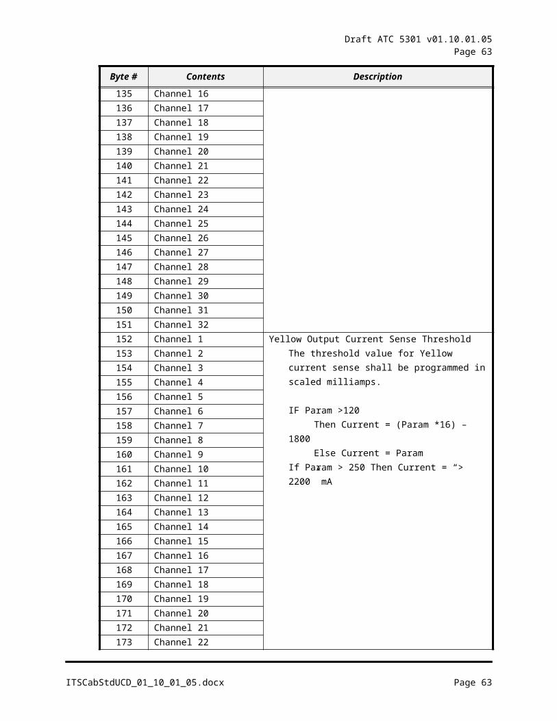
Draft ATC 5301 v01.10.01.05Page 63
Connector Type and Pin Assignments YesMechanical Dimensions Yes
6.7.1 General
The Sensor Unit functions as an input device used to sense field status conditions such as: NEMA 2-Channel Inductive Loop Detector with (2) Outputs and (2) Status NEMA 4-Channel Inductive Loop Detector with (4) Outputs and (4) Status Type 222 Inductive Loop Detector with (2) channels without Status Type 224 Inductive Loop Detector with (4) channels without Status Type 242L DC Isolator with (2) channels and (2) Status Type 244L DC Isolator with (4) channels and (4) Status Preemptor
6.7.2 Form Factor
Sensor Unit form factor shall conform to NEMA TS2 standard, Section 6.5.2.2.2 (see Figure 6-5)
6.7.3 Connector and Pin Assignments
Sensor Unit connector and pin assignments shall conform to NEMA TS2 standard Section 6.5.2.28 (see Table 6-2) for NEMA 4-Channel Inductive Loop Detector with (4) Outputs and (4) Status without INBUS.
For other Sensor Units listed in 6.7.1 above, the Loop connector pins shall be used for field wire inputs according to the sensor product specifications.
7 SLOTS
Slots include mechanical mounting hardware and electrical connectors necessary to house interchangeable assemblies.
7.1 Serial Interface Unit Slot
Standardization LevelDescription Controlled by Standard?
Interface Signal Names and Electrical Characteristics YesConnector Type and Pin Assignments YesMechanical Dimensions Yes
7.1.1 General
The model 2218 Slot functions to mechanically mount and to electrically connect the Serial Interface Unit (SIU)
7.1.2 Form Factor
The model 2218 Slot Form Factor shall mechanically and electrically accommodate the model 2218 as shown:
ITSCabStdUCD_01_10_01_05.docx Page 63

Draft ATC 5301 v01.10.01.05Page 64
Figure 9: model 2218 Slot Mechanical Details
The model 2218 Slot shall be capable of being shelf mounted or in a EIA 482.6 mm (19 in.) rack (EIA Standard RS-310) and shall not exceed 152.40 mm (6.0 in.) in height and have a maximum depth of 215.90 mm (8.50 in.).
Refer to model 2218 section of this standard for horizontal dimension from card guide centerline to centerline of model 2218 circuit board
7.1.3 Connector and Pin Assignments
Refer to model 2218 section of this standard for mating connector type, orientation and pin assignments
7.2 Cabinet Monitor Unit Slot
Standardization LevelDescription Controlled by Standard?
Interface Signal Names and Electrical Characteristics YesConnector Type and Pin Assignments YesMechanical Dimensions Yes
ITSCabStdUCD_01_10_01_05.docx Page 64
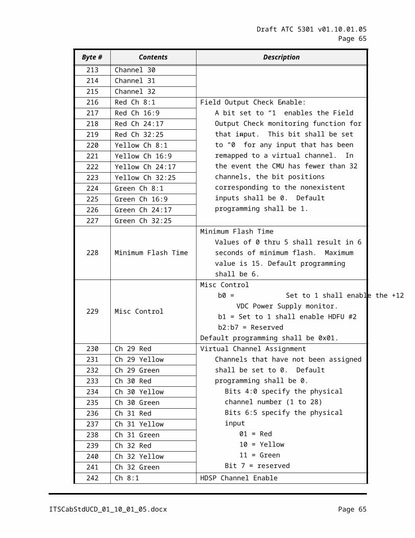
Draft ATC 5301 v01.10.01.05Page 65
7.2.1 General
CMU2212 Slot functions to mechanically mount and to electrically connect the Cabinet Monitor Unit (CMU).
7.2.2 Form Factor
CMU2212 Slot Form Factor shall mechanically and electrically accommodate the CMU2212 as shown:
Figure 10: CMU Slot Mechanical Details
1. CMU2212 connector shall be a DIN 64S or equivalent. 2. Refer to CMU2212 section of this standard for horizontal dimension from card guide centerline to
centerline of CMU2212 circuit board.
7.2.3 Connector and Pin Assignments
Refer to CMU2212 section of this standard for connector pin assignments
7.3 IN Slot
Standardization LevelDescription Controlled by Standard?
Interface Signal Names and Electrical Characteristics YesConnector Type and Pin Assignments YesMechanical Dimensions Yes
7.3.1 General
IN Slot functions to mechanically mount and to electrically connect the Sensors.
ITSCabStdUCD_01_10_01_05.docx Page 65
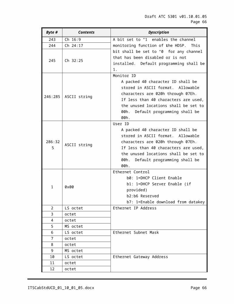
Draft ATC 5301 v01.10.01.05Page 66
7.3.2 Form Factor
Figure 11: IN Slot Mechanical Details
The IN Slot shall be capable of being shelf mounted or in a EIA 482.6 mm (19 in.) rack (EIA Standard RS-310) and shall not exceed 152.40 mm (6.0 in.) in height and have a maximum depth of 215.90 mm (8.50 in.).
The IN Slot shall provide a 44 terminal, double row, 3.962 mm (0.156 in.) contact spacing, Cinch Jones card edge connector 50-44A-30M, or equivalent centered vertically for each Sensor module.
7.3.3 Connector and Pin Assignments
Refer to Sensor section of this standard for connector orientation and pin assignments
7.4 OUT Slot
Standardization LevelDescription Controlled by Standard?
Interface Signal Names and Electrical Characteristics YesConnector Type and Pin Assignments YesMechanical Dimensions Yes
7.4.1 General
OUT Slot functions to mechanically mount and to electrically connect the High Density Switch Pack Flasher Unit
ITSCabStdUCD_01_10_01_05.docx Page 66
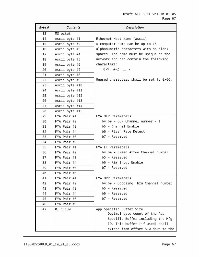
Draft ATC 5301 v01.10.01.05Page 67
7.4.2 Form Factor
OUT Slot Form Factor shall mechanically and electrically accommodate the output devices as shown:
Figure 12: OUT Slot Mechanical Details
7.4.3 Connector and Pin Assignments
Refer to Model 2202 HDSP/FU section of this standard for mating connector type, orientation and pin assignments.
8 INTERFACES
Interfaces interconnect system elements shown in the Block Diagrams.
8.1 SIU IN Interface
Standardization LevelDescription Controlled by Standard?
Interface Signal Names and Electrical Characteristics YesConnector Types and Pin Assignments of model 2218 Slot and Sensor Slot
Yes
Mechanical Dimensions of the interface from model 2218 Slot to Sensor Slots
No
ITSCabStdUCD_01_10_01_05.docx Page 67
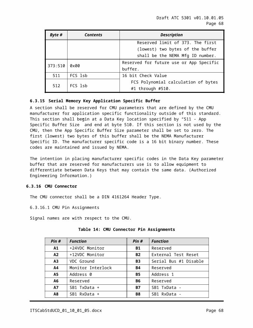
Draft ATC 5301 v01.10.01.05Page 68
8.1.1 General
The SIU IN interface functions to electrically connect the IN SLOT connectors to the SIU connectors.
8.1.2 Electrical Characteristics
Refer to the model 2218 section of this standard for the electrical characteristics of the model 2218 IN signals, shown below. model 2218 IN INPUT / OUTPUT TRANSISTOR continually OFF (passively pulled up to 24 VDC). The Sensor plugged into the IN SLOT asserts the INPUT / OUTPUT by actively pulling the INPUT / OUTPUT pin to 0 volts (Ground True). The Sensor deasserts the model 2218 IN signal from the Sensor in IN SLOT by releasing the signal (OFF), allowing the resistor to actively pull the signal to +24 V.
Figure 13: model 2218 IN Interface Block Diagram
8.1.3 Form Factor
SIU IN mechanical connection from SIU to Sensor Slots is not controlled by this standard
8.1.4 SIU 1 Pin Assignments
Detector functions for channels 25-120 shall be assigned to Input SIU 2 through 5 in the same sequence as shown in Table 20. Channel 1 and Channel 2 shall be located in Slot #1 and increment sequentially. Signal names are with respect to the Controller Unit.
The Detector Reset outputs shall be connected to pin C of both assigned slots to provide for a two channel or four channel detector reset function.
Table 20: SIU 1 to IN SLOT Signal Mapping
INPUT SIU 1Row A Row B Row C
Pin#
Pin Name
Function Pin Name
Function Pin Name
Function
1 +24V POWER +24V POWER IO 47 CHANNEL 18 STATUS
ITSCabStdUCD_01_10_01_05.docx Page 68
SIU-2218 IN
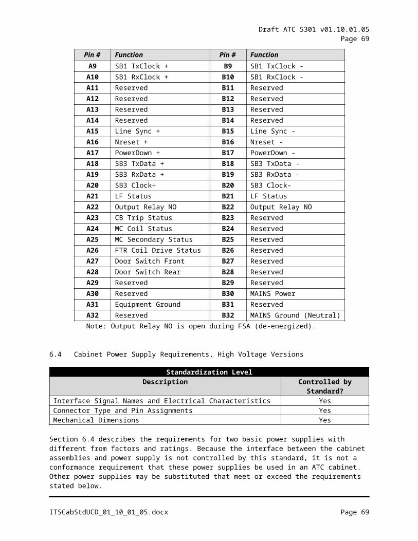
Draft ATC 5301 v01.10.01.05Page 69
INPUT SIU 1Row A Row B Row C
Pin#
Pin Name
Function Pin Name
Function Pin Name
Function
2 IO 0 CHANNEL1-4 RESET IO 1 CHANNEL 5-8 RESET IO 48 CHANNEL 19 STATUS3 IO 2 CHANNEL9-12
RESETIO 3 CHANNEL13-16
RESETIO 49 CHANNEL 20 STATUS
4 IO 4 CHANNEL17-20 RESET
IO 5 CHANNEL 21-24 RESET
IO 50 CHANNEL 21 STATUS
5 IO 6 CHANNEL 1 OUT IO 7 CHANNEL 2 OUT IO 51 CHANNEL 22 STATUS6 IO 8 CHANNEL 3 OUT IO 9 CHANNEL 4 OUT IO 52 CHANNEL 23 STATUS7 IO 10 CHANNEL 5 OUT IO 11 CHANNEL 6 OUT IO 53 CHANNEL 24 STATUS8 IO 12 CHANNEL 7 OUT IO 13 CHANNEL 8 OUT SB1
RXD+9 IO 14 CHANNEL 9 OUT IO 15 CHANNEL 10 OUT SB1
RXD-10 IO 16 CHANNEL 11 OUT IO 17 CHANNEL 12 OUT SB1
TXD+11 IO 18 CHANNEL 13 OUT IO 19 CHANNEL 14 OUT SB1
TXD-12 IO 20 CHANNEL 15 OUT IO 21 CHANNEL 16 OUT SB1
RXC+13 IO 22 CHANNEL 17 OUT IO 23 CHANNEL 18 OUT SB1
RXC-14 IO 24 CHANNEL 19 OUT IO 25 CHANNEL 20 OUT SB1
TXC+15 IO 26 CHANNEL 21 OUT IO 27 CHANNEL 22 OUT SB1
TXC-16 IO 28 CHANNEL 23 OUT IO 29 CHANNEL 24 OUT LSYNC+17 IO 30 CHANNEL 1 STATUS IO 31 CHANNEL 2 STATUS LSYNC-18 IO 32 CHANNEL 3 STATUS IO 33 CHANNEL 4 STATUS NRESET
+19 IO 34 CHANNEL 5 STATUS IO 35 CHANNEL 6 STATUS NRESET
-20 IO 36 CHANNEL 7 STATUS IO 37 CHANNEL 8 STATUS ASSY
ADR21 IO 38 CHANNEL 9 STATUS IO 39 CHANNEL 10 STATUS INBUS
RTS22 IO 40 CHANNEL 11
STATUSIO 41 CHANNEL 12 STATUS SB2
RXD+23 IO 42 CHANNEL 13
STATUSIO 43 CHANNEL 14 STATUS SB2
RXD-24 IO 44 CHANNEL 15
STATUSIO 45 CHANNEL 16 STATUS SB2
TXD+25 IO 46 CHANNEL 17
STATUSOPTO IN 1
PED1 SB2 TXD-
26 OPTO IN 2
PED2 OPTO IN 3
PED3 SB2 RXC+
27 OPTO IN 4
PED4 OPTO GND
PED GND SB2 RXC-
28 ADR 0 ADR 1 SB2 TXC+
29 ADR 2 ADR 3 SB2 TXC-
30 INBUS TXD
INBUS RXD
INBUS TXC
31 EQGND
AC LINE REF
INBUS RXC
ITSCabStdUCD_01_10_01_05.docx Page 69

Draft ATC 5301 v01.10.01.05Page 70
INPUT SIU 1Row A Row B Row C
Pin#
Pin Name
Function Pin Name
Function Pin Name
Function
32 DCGND2
DCGND2
DCGND2
8.2 SIU OUT Interface
Standardization LevelDescription Controlled by Standard?
Interface Signal Names and Electrical Characteristics YesConnector Types and Pin Assignments of SIU Slot and Load Switch Slot YesMechanical Dimensions of the interface from SIU Slot to Load Switch Slot No
8.2.1 General
The SIU OUT interface functions to electrically connect the OUT SLOT connectors to the SIU connectors.
8.2.2 Electrical Characteristics
Refer to the model 2218 section of this standard for the electrical characteristics of the model 2218 OUT signals, shown below. model 2218 OUT INPUT / OUTPUT PIN is asserted when the OUTPUT TRANSISTOR is ON (0 volts). model 2218 OUT INPUT / OUTPUT PIN is unasserted when the OUTPUT TRANSISTOR is OFF (passively pulled up to 24 VDC).
Figure 14: model 2218 OUT Electrical Characteristics
8.2.3 Form Factor
ITSCabStdUCD_01_10_01_05.docx Page 70
Draft ATC 5301 v01.10.01.05Page 71
The mechanical form factor of the OUT SLOT interface to the Load Switches and Flasher is not controlled by this standard.
8.2.4 Connector Pin Assignments
Control and Serial Bus #1 signal names are with respect to the Controller Unit.
Table 21: First Output SIU Opto AssignmentsPin First Output Assembly Housing TypeOpto Input 1 Manual Control Enable AllOpto Input 2 Interval Advance AllOpto Input 3 Stop Time AllOpto Input 4 Manual Flash AllOpto Input Common 48VDC All
Table 22: model 2218 to OUT SLOT Signal Mapping
Switch Pack SP1- SP8Row A Row B Row C
Pin
Pin Name Switch Pack Pin Name Switch Pack Pin Name Switch Pack
1 +24V +24V IO 47 SP8 CH2 RED 2 IO 0 SP1 CH1 RED IO 1 SP1 CH1 YEL IO 48 SP8 CH2 YEL3 IO 2 SP1 CH1 GRN IO 3 SP1 CH2 RED IO 49 SP8 CH2 GRN4 IO 4 SP1 CH2 YEL IO 5 SP1 CH2 GRN IO 505 IO 6 SP2 CH1 RED IO 7 SP2 CH1 YEL IO 516 IO 8 SP2 CH1 GRN IO 9 SP2 CH2 RED IO 527 IO 10 SP2 CH2 YEL IO 11 SP2 CH2 GRN IO 538 IO 12 SP3 CH1 RED IO 13 SP3 CH1 YEL SB1 RXD+9 IO 14 SP3 CH1 GRN IO 15 SP3 CH2 RED SB1 RXD-
10 IO 16 SP3 CH2 YEL IO 17 SP3 CH2 GRN SB1 TXD+11 IO 18 SP4 CH1 RED IO 19 SP4 CH1 YEL SB1 TXD-12 IO 20 SP4 CH1 GRN IO 21 SP4 CH2 RED SB1 RXC+13 IO 22 SP4 CH2 YEL IO 23 SP4 CH2 GRN SB1 RXC-14 IO 24 SP5 CH1 RED IO 25 SP5 CH1 YEL SB1 TXC+15 IO 26 SP5 CH1 GRN IO 27 SP5 CH2 RED SB1 TXC-16 IO 28 SP5 CH2 YEL IO 29 SP5 CH2 GRN LSYNC+17 IO 30 SP6 CH1 RED IO 31 SP6 CH1 YEL LSYNC-18 IO 32 SP6 CH1 GRN IO 33 SP6 CH2 RED NRESET+19 IO 34 SP6 CH2 YEL IO 35 SP6 CH2 GRN NRESET-20 IO 36 SP7 CH1 RED IO 37 SP7 CH1 YEL ASSY ADR21 IO 38 SP7 CH1 GRN IO 39 SP7 CH2 RED INBUS RTS22 IO 40 SP7 CH2 YEL IO 41 SP7 CH2 GRN SB2 RXD+23 IO 42 SP8 CH1 RED IO 43 SP8 CH1 YEL SB2 RXD-24 IO 44 SP8 CH1 GRN IO 45 -- SB2 TXD+25 IO 46 -- OPTO IN 1 MCE SB2 TXD-26 OPTO IN 2 INTER ADV OPTO IN 3 STOP TIME SB2 RXC+27 OPTO IN 4 LOC FLASH OPTO GND FACIL GND SB2 RXC-28 ADR 0 ADR 1 SB2 TXC+29 ADR 2 ADR 3 SB2 TXC-
ITSCabStdUCD_01_10_01_05.docx Page 71
Draft ATC 5301 v01.10.01.05Page 72
30 INBUS TXD
INBUS RXD INBUS TXC
31 EQGND AC LINE REF INBUS RXC32 DCGND2 DCGND2 DCGND2
8.3 SB1/SB2 Interface
Standardization LevelDescription Controlled by
Standard?Interface Signal Names and Electrical Characteristics YesConnector Types and Pin Assignments YesMechanical Dimensions of the interface from model 2218 to Controller Unit No
8.3.1 General
8.3.1.1Serial Bus 1
Serial Bus #1 (SB1) communicates real-time information required to operate the system. It handles the highest priority, time-sensitive data exchange between the SIUs in the input and output assemblies, controller unit and the CMU. An example would be the commands to the switch packs to change signal color or data from detection inputs. SB1 is designed for a communications rate of 614,400 bits per second.
8.3.1.2Serial Bus 2
Serial Bus #2 (SB2) communicates less time critical information between the Controller Unit and sensors in the input assemblies. An example would be direct communications of detector tuning and sensing of detector CALLS from the Controller Unit. Serial bus 2 is designed for an allowable communications rate of 614,400 bits per second.
8.3.1.3Terminator Unit
An SB1 and SB2 terminator unit shall be provided. There are two acceptable methods for implementing termination. Method #1 is accomplished by installing the terminator unit into the DC POWER / COMMUNICATIONS ASSEMBLY DB 25S End Connector if that assembly is provided in the cabinet. Method #2 is accomplished by installng the termination unit into the "THROUGH" connector of the last assembly connected to the SB1/ SB2 serial chain when a serial "Daisy Chain" method, consisting of "IN" and "THROUGH" on each assembly is used. The source of +5VDC and Ground for powering the termination bias resistors shall be derived from Pins 12 and 13, respectively, of the SB1 / SB2, 25-pin, D-Sub connector.The terminator unit shall provide a 150 ohm termination resistor between the RxD+ and RxD-, the TxD+ and TxD-, the RxC+ and RxC-, and the TxC+ and TxC- pairs for both serial bus #1 and serial bus #2. The terminator unit shall also provide 1K ohm DC bias resistors from +5VDC ISO to the RxD+, the RxC+, the TxD+, and the TxC+ of both serial bus #1 and serial bus #2. The terminator unit shall provide 1K ohm DC bias resistors from ISO GND to the RxD-, the RxC-, the TxD-, and the TxC- of both serial bus #1 and serial bus #2.
8.3.1.4Form Factor
SB1 and SB2 are included in one SB1/SB2 physical interface consisting of a single communications cable terminated by 25 pin “D” connectors at each end.
ITSCabStdUCD_01_10_01_05.docx Page 72

Draft ATC 5301 v01.10.01.05Page 73
Figure 15: SB1/SB2 Communications Interface Form Factor
ITSCabStdUCD_01_10_01_05.docx Page 73
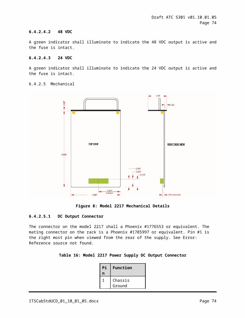
Draft ATC 5301 v01.10.01.05Page 74
Figure 16: SB1/SB2 Terminator Unit
R3 value is selected to match the bus characteristic impedance. R1 = R2 value is selected to bias the receivers to MARK state when not driven. Values shown may be adjusted for the ATCC design.
ITSCabStdUCD_01_10_01_05.docx Page 74
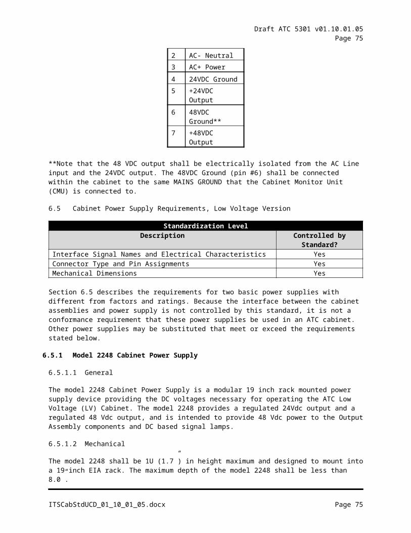
Draft ATC 5301 v01.10.01.05Page 75
8.3.2 Connector Pin Assignment
Table 23: SB1/SB2 Connector Pin Assignment
Pin AT the CU AT the SIU1 SB1 TxD+ SB1 RxD+2 SB1 RxD+ SB1 TxD+3 SB1 TxC+ SB1 RxC+4 SB1 RxC+ SB1 TxC+5 SB2 TxD+ SB2 RxD+6 SB2 RxD+ SB2 TxD+7 SB2 TxC+ SB2 RxC+8 SB2 RxC+ SB2 TxC+9 LINE SYNC+ LINE SYNC+
10 NRESET+ NRESET+11 POWER DOWN+12 +5 VDC ISO13 ISO GND14 SB1 TxD- SB1 RxD-15 SB1 RxD- SB1 TxD-16 SB1 TxC- SB1 RxC-17 SB1 RxC- SB1 TxC-18 SB2 TxD- SB2 RxD-19 SB2 RxD- SB2 TxD-20 SB2 TxC- SB2 RxC-21 SB2 RxC- SB2 TxC-22 LINE SYNC- LINE SYNC-23 NRESET- NRESET-24 POWER DOWN-25 EQ GND
8.4 B3 Interface
Standardization LevelDescription Controlled by Standard?
Interface Signal Names and Electrical Characteristics YesConnector Types and Pin Assignments YesMechanical Dimensions of the interface from CMU to Load Switches No
8.4.1 General
The 2202 HDSP/FU shall respond to serial data frames transmitted by the CMU-2212 on the Serial Bus #3
ITSCabStdUCD_01_10_01_05.docx Page 75
Draft ATC 5301 v01.10.01.05Page 76
8.4.2 SB3 Terminations
No termination loads shall be provided by the 2202 HDSP/FU. Serial Bus #3 termination is provided by the CMU2212 (RXD) and the ADU (TXD).
8.4.3 SB3 Electrical
The 2202 HDSP/FU Serial Bus #3 shall consist of two interface links (TXD +/- and RXD +/-) conforming to the requirements of the Electronic Industries Association EIA-485, Standard for Electrical Characteristics of Generators and Receivers for use in Balanced Digital Multipoint Systems, dated April 1983. Where differences occur between the EIA-485 standard and this document, this document shall govern.
2202 HDSP/FU SB#3 RX +/- shall be inputs to the 2202 HDSP/FU from the CMU-2212. 2202 HDSP/FU SB#3 TXD +/- shall be outputs to the CMU-2212 from the 2202 HDSP/FU. All voltage potentials on the 2202 HDSP/FU SB#3 interface shall be referenced to MAINS Ground.
8.4.4 Form Factor
SB3 interface on cabinet shall consist of (2) RJ-11 sockets wired in parallel for daisy-chain:
Figure 17: SB3 Communications Interface Form Factor
SB3 interface cable shall consist of (2) RJ-11 plugs on sheathed, color coded cable
SB3RJ-11PLUG
RJ-11PLUG
Figure 18: SB3 Communications Cable Form Factor
8.4.5 Connector Pin Assignments
Table 24: SB #3 Connector Pin Assignment
ITSCabStdUCD_01_10_01_05.docx Page 76
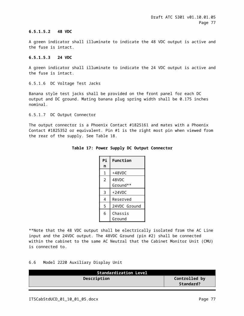
Draft ATC 5301 v01.10.01.05Page 77
Pin Pair Color AT the CU AT the SIU1 White Orange SB3 TxC+ SB3 RxC+2 Orange SB3 TxC- SB3 RxC-3 White Green Service- RAW Service- RAW4 Blue SB3 TxD+ SB3 RxD+5 White Blue SB3 TxD- SB3 RxD-6 Green Service- RAW Service- RAW7 White Brown SB3 RxD+ SB3 TxD+8 Brown SB3 RxD- SB3 TxD-
8.5 CC Interface
Standardization LevelDescription Controlled by Standard?
Interface Signal Names and Electrical Characteristics YesConnector Types and Pin Assignments YesMechanical Dimensions of the interface from CMU to Door Switch No
8.5.1 General
The Cabinet Control (CC) interface functions to electrically connect the Cabinet Monitor Unit (CMU) to the Door Switch, Police Panel switches and to the Output Functionality.
8.5.2 Form Factor
The CC Interface shall use a Molex 0003091157, with pin number 0002091119, or equivalent intermatable connector on one end and is either hardwired to the appropriate door and police panel switches on the other end or is point-to-point, parallel, wired to an identical connector on the other end, depending on cabinet architecture. AWG-18 wire shall be used for all conductors. . Free swinging cables shall always be sheathed while fixed cable bundles need only be dressed with zip ties or lacing twine
1
2
3
4
5
6
7
8
9
10
11
12
13
14
15
1
2
3
4
5
6
7
8
9
10
11
12
13
14
15
CC
Figure 19: CC Interface Form Factor
ITSCabStdUCD_01_10_01_05.docx Page 77

Draft ATC 5301 v01.10.01.05Page 78
8.5.3 Connector Pin Assignments
Table 25: CC Connector Pin Assignments
Pins Function1 - 1 MC Coil from PP2 - 2 48 VDC to PP and Fan3 - 3 TR Coil from PP4 - 4 Signal Flash5 - 5 Front Door Switch6 - 6 From Auto Flash Switch7 – 7 Reserved8 – 8 From Rear Door Switch9 – 9 CB Trip Status CMU to PP
10 -10 N.C.11 – 11 GND12 – 12 +48VDC13 – 13 MANUAL CONTROL EN In14 – 14 INTERVAL ADV Out15 - 15 STOP TIME Switch
ITSCabStdUCD_01_10_01_05.docx Page 78
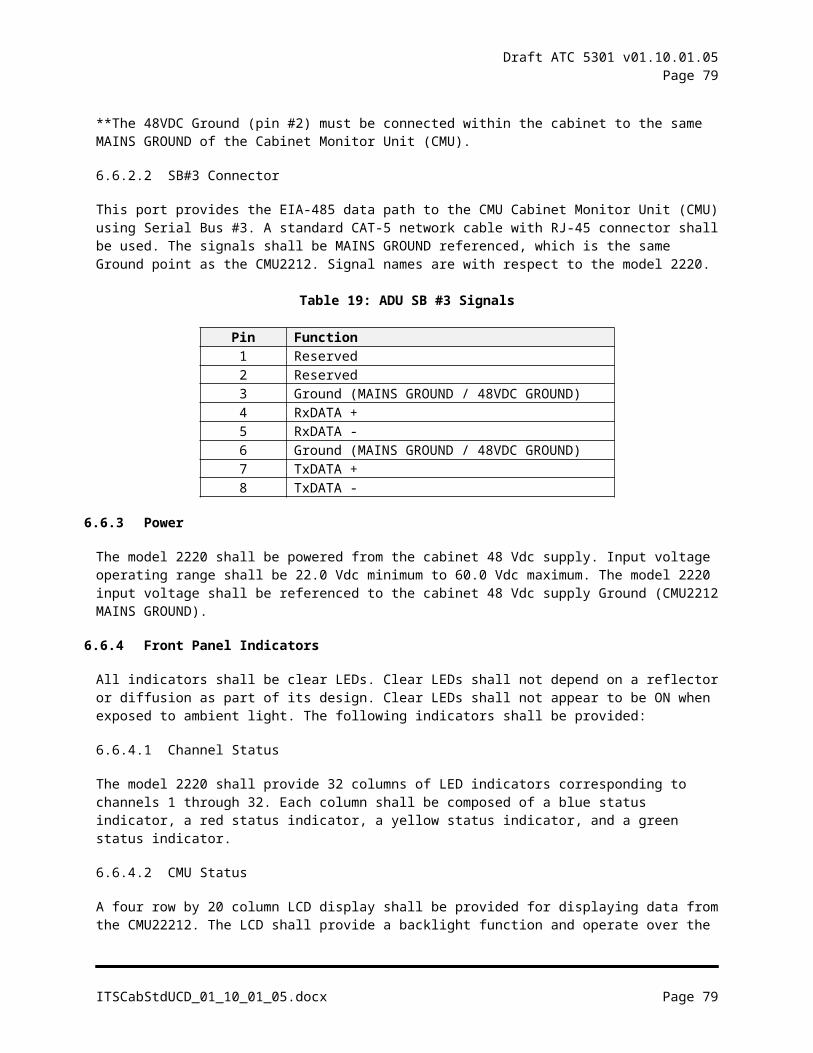
Draft ATC 5301 v01.10.01.05Page 79
Figure 20: CC Interface Connection Diagram
8.6 CDC Interface
Standardization LevelDescription Controlled by Standard?
Interface Signal Names and Electrical Characteristics Yes
ITSCabStdUCD_01_10_01_05.docx Page 79
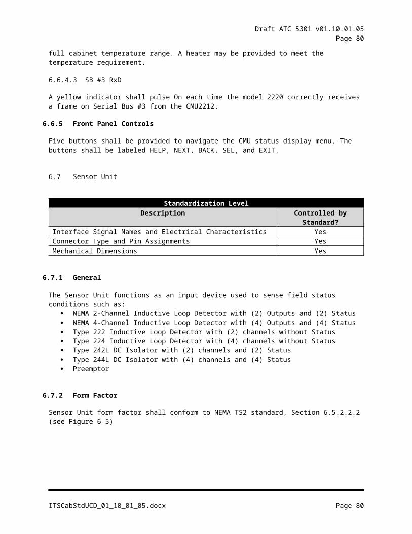
Draft ATC 5301 v01.10.01.05Page 80
Connector Types and Pin Assignments YesMechanical Dimensions of the interface from model 2218 to Police Panel No
8.6.1 General
The Cabinet D Connector (CDC) interface functions to provide access to the four opto-isolator inputs on each Input Functionality SIU. These inputs may be used to facilitate isolated pedestrian switch signals or other signals requiring isolation.
The CDC interface is optional, but if included, shall conform to this section of the standard.
8.6.1.1Output SIU #1 Opto Inputs
The Manual Control Enable and Manual Flash switch and Interval Advance and Stop Time switch signals shall be a 48Vdc signal without a series resistor. They shall be low voltage signals tied to Service - RAW. CDC pin 5 common shall be referenced to Service- RAW. CDC pin 8 shall provide an interface for the external reset signal and CDC pin 9 shall provide an interface for DC Ground 2.
8.6.1.2Form Factor
The CDC Interface consists of 9-pin “D” plugs parallel wired (point to point) with #18 gauge minimum wire size.
Figure 21: CDC Interface Form Factor
8.6.1.3CDC Connector Pin Assignments
Table 26: CDC Connector Pin Assignments
DB9P-1 Function DB9P-2 Function1 Opto 1 1 Opto 12 Opto 2 2 Opto 23 Opto 3 3 Opto 34 Opto 4 4 Opto 45 Opto Common 5 Opto Common6 NC 6 NC7 NC 7 NC8 Spare 8 Spare9 Spare 9 Spare
ITSCabStdUCD_01_10_01_05.docx Page 80
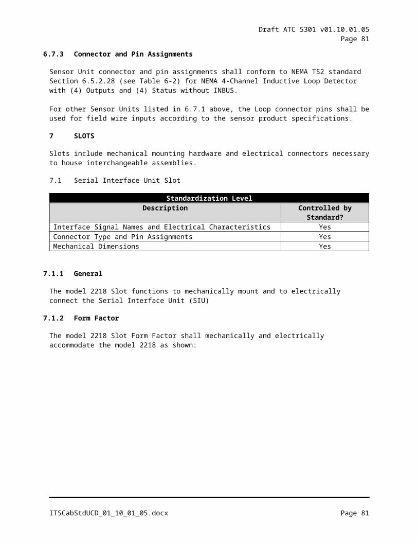
Draft ATC 5301 v01.10.01.05Page 81
8.7 Termination Interface
Standardization LevelDescription Controlled by Standard?
Interface Signal Names and Electrical Characteristics YesConnector Types and Pin Assignments YesMechanical Dimensions of the interface from OUT SLOT to Field Wires No
8.7.1 General
The Termination interface functions to: Provide the electrical connection point between the Signal Head Field Wires and the Output
Functionalities' OUT SLOT connectors Physically program the signal flash either as RED or YELLOW
Under control of the CMU,select between the HDSPs or the Flasher, as the source for feeding the signal field wires.
8.7.2 Electrical Characteristics
The electrical characteristics and signals of the Termination interface shall be controlled by the standard. The Termination Interface shall electrically conform to Figure 22 , which depicts the circuitry required for each High Density Switch Pack, in a cabinet assembly, which provides two channels of RED, YELLOW, and GREEN outputs (six physical outputs.
Figure 22: Termination Interface for 2 Load Switch Channels
ITSCabStdUCD_01_10_01_05.docx Page 81
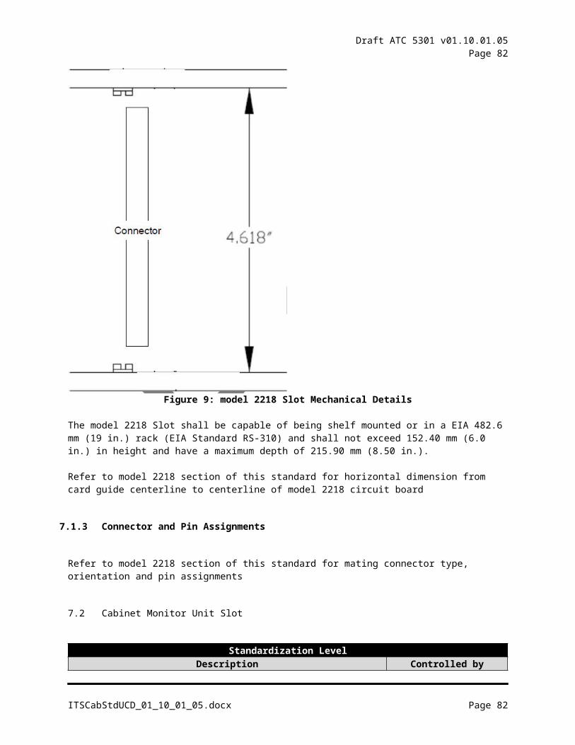
Draft ATC 5301 v01.10.01.05Page 82
8.7.2.1OUT SLOT Interface
The OUT SLOT interface shall electrically connect to its associated OUT SLOT located on the Output Functionality. The HDSP in that slot controls two sets of RED, YELLOW and GREEN signal indicators.
8.7.2.2Flash Programming Blocks
Each flash programming block shall provide Flash Programming for its HDSP channel. The FPs shall accept RED plugs to program RED flash and shall accept YELLOW plugs to program YELLOW flash as shown in Figure 22. When a Red plug is installed, the Red signal from its associated HDSP shal be routed through the FTR contacts allowing the FTR to select either the HDSP Red signal or the Flasher signal to be routed to the Field Wire Interface. Yellow flash plugs shall operate in a similar manner. FP1, FP2 and the programming jumpers shall be electrically sized for the load.
8.7.2.3Flash Transfer Relay (FTRn)
FTR1 Flash Transfer Relay shall provide Flash Transfer that: Connects FTR1 field wires and FTR2 field wires to the load switch when the FTR1 coil is
energized Connects FTR1 field wires and FTR2 field wires to FL PWR 1 flasher power when the FTR1 coil
is de-energized. Connects one side of the FTR1 coil to SERVICE VOLTAGE- Connects the other side of the FTR1 coil to FS signal controlled by the CMU
The FR1 contacts shall be electrically sized for the load. The FTR coil pull-in and drop-out specifications shall provide operation as described above over the service voltage operating range.
8.7.3 Field Wire Sense
Each HDSP includes a sense wire input associated with each of its outputs. The Field Wire Sense Interface shall provide a connection between the HDSP sense inputs and the field wires attached to the Field Wire Interface. The conductors of the Field Wire Sense Interfaces shall be attached as close as possible to the field wire terminals. The sense conductors shall be non current-carrying providing a remote measurement of the field wire voltage that avoids the IR voltage drop.
8.7.3.1Flash Sense Interface
Each HDFU includes a sense wire input associated with each of its outputs. The Flasher Wire Sense Interface shall provide a connection between the HDFU sense inputs and the Flash Signal inputs of the FTRs. The conductors of the Flasher Sense Interfaces shall be attached as close as possible to the FTR terminals. The sense conductors shall be non current-carrying providing a remote measurement of the field wire voltage that avoids the IR voltage drop.
8.7.4 Form Factor
The mechanical form factor of the Termination interface is not controlled by this standard, including the flash programming blocks, flash transfer relay and connectors.
8.7.5 Field Wire Interface
The Field Wire Interface connects the loads controlled by the ATCC. The Field Wire Interface conductors and contacts shall be electrically sized for a minimum of 3 Amps.
ITSCabStdUCD_01_10_01_05.docx Page 82
Draft ATC 5301 v01.10.01.05Page 83
9 PROTOCOLS
9.1 SB1 Communications Protocol
9.1.1 Electrical
The Serial Bus #1 shall consist of four interface links (TXD +/- and RXD +/-, TXC +/- and RXC +/-) conforming to the requirements of the Electronic Industries Association EIA-485, Standard for Electrical Characteristics of Generators and Receivers for use in Balanced Digital Multipoint Systems, dated April 1983. Where differences occur between the EIA-485 standard and this document, this document shall govern.
All voltage potentials on the SB#1 interface shall be referenced to +24VDC Ground.
9.1.2 Data Link Layer
The data link layer protocol is based on a subset of HDLC as defined by ISO/IEC 13239:2002. Each frame shall consist of the following fields:Flag byte = 0x7EAddress byte = 0x01 through 0x20Control byte = 0x13 (U Format)Information field = defined below in Sections 9.1.5, 9.1.6, and 9.1.7Frame Check Sequence = 16 bit FCS procedure defined in clause 2.5.2 of ISO/IEC 13239:2002.Flag byte = 0x7E
Transmission shall be in synchronous mode as defined by clause 4.3.1 of ISO/IEC 13239:2002. The format shall be 8 bit data at 614,000 bits per second (+/-2%).
9.1.3 Procedures
Frames transmitted by the ATC shall be referred to as command frames and frames transmitted by the secondary stations shall be referred to as response frames. Response frames shall only be transmitted as a result of correctly receiving a command frame. The first eight bits in each information field shall contain the Frame Type number.
Reserved bits in any message shall always be set to zero by the transmitting station.
9.1.4 Message Timing
The secondary station shall begin its response to command frames from the ATC within a designated period of time following the correct reception of a complete command frame including the closing flag. This period shall be known as the Service Time and shall have a maximum value of 50 microseconds. The secondary station link output shall be in the high impedance state outside of the interval defined by the Service Time plus Response Time.
The secondary station shall complete its transmission of the response frame including the closing flag within a designated time known as the Response Time, depending on the number of bytes transmitted in the response frame. The secondary station link output shall transition to a high impedance state a maximum of 25 microseconds following the transmission of the closing flag.
Following the transmission of each command frame, there shall be a Dead Time during which the ATC does not transmit. This Dead Time shall be a minimum of the Service Time plus the Response Time.
ITSCabStdUCD_01_10_01_05.docx Page 83
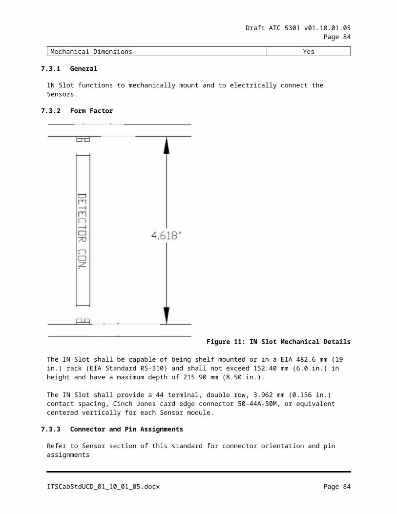
Draft ATC 5301 v01.10.01.05Page 84
9.1.5 SB1 Frame Types
The frame type shall be determined by the value of the first byte of the message. The command frames type values $70 - $7F and associated response frame type values $F0 - $FF are allocated to the manufacturer diagnostics. All other frame types not called out are reserved. The command-response frame type values and message times shall be as follows:
Table 27: Frame Types and Performance Requirements
ModuleCommand
I/0 ModuleResponse Description Destination Device
49 177 Request Module Status SIU50 178 MILLISECOND CTR. Mgmt. SIU51 179 Configure Inputs SIU52 180 Poll Raw Input Data SIU53 181 Poll Filtered Input Data SIU54 182 Poll Input Transition Buffer SIU55 183 Command Outputs SIU56 184 Configure Input Tracking Functions SIU57 185 Configure Complex Output Functions SIU58 186 Reserved --59 187 Reserved --60 188 Module Identification SIU, CMU61 189 Reserved (deprecated) --62 190 Send to Local Flash CMU63 191 Reserved --64 192 Reserved --65 193 Reserved (deprecated) --66 --- Time / Date ALL67 195 Switch Pack Drivers (short) CMU80 208 Module Description SIU, CMU81 209 Switch Pack Drivers (long) CMU82 210 CMU Configuration CMU
Messages 62/190, 67/195, 81/209, and 82/210 shall be for the ATC Cabinet Monitor Unit. See Model 2212 Cabinet Monitor Unit Serial Bus #1 section 9.1.7 for command and response frames. Message 66/No-Response is a broadcast message to Address 255 containing the current time. Any device may receive and process this message if it has the software capacity.
9.1.5.1Module Identification
The Module Identification command frame shall be used to request the identification value for the SIU and CMU. Reply message shall use the following addresses: ATC field I/Os shall respond with address 20. SIUs respond with their own address ranging from 0-14. CMUs respond with their own addresses, ranging from 15-18.
The command and response frames shall be shown as follows:
Table 28: Module Identification Command
Description msb lsb Byte Number(Type Number= 60) 0 0 1 1 1 1 0 0 Byte 1
ITSCabStdUCD_01_10_01_05.docx Page 84
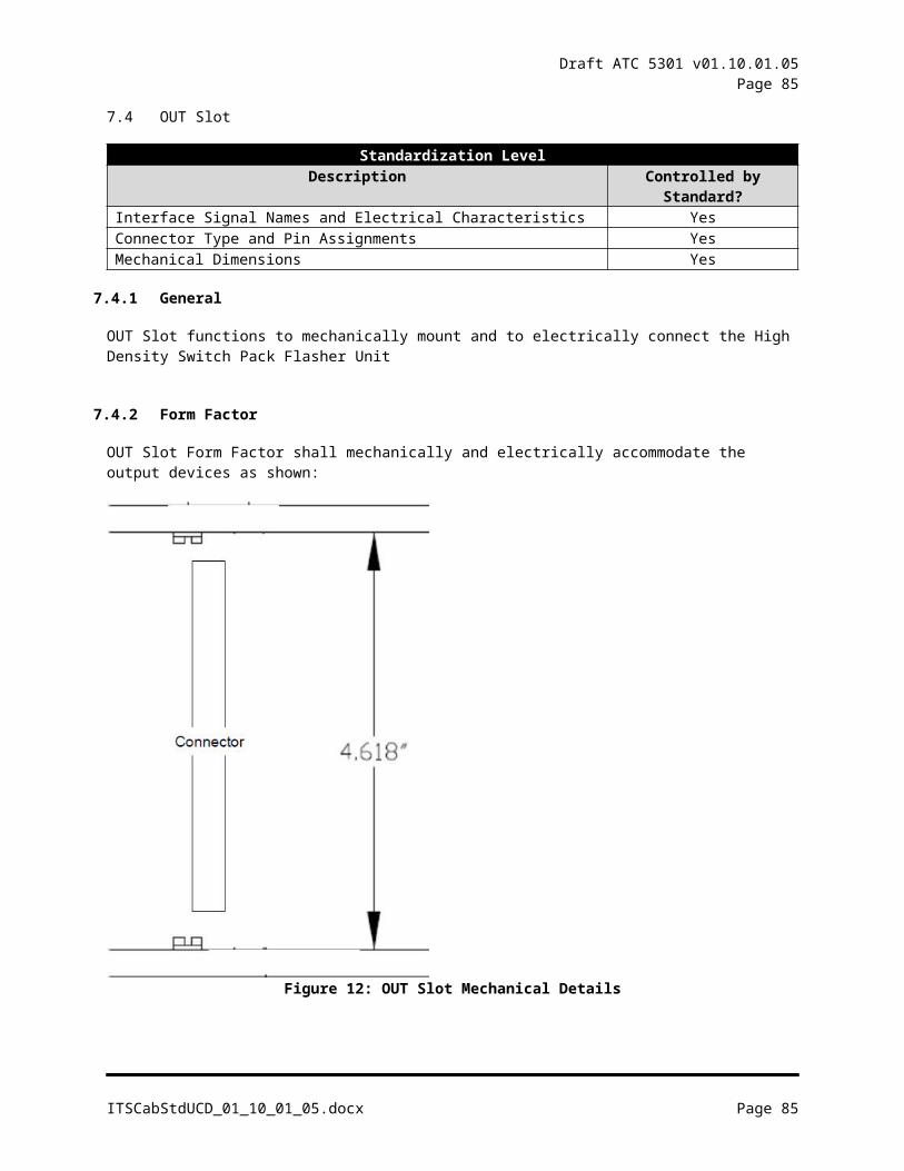
Draft ATC 5301 v01.10.01.05Page 85
Table 29: Module Identification Response
Description msb lsb Byte Number(Type Number= 188) 1 0 1 1 1 1 0 0 Byte 1model 2218 ID byte x x x x x x x x Byte 2
9.1.5.2Type 66 Command _Time and Date Broadcast
Table 30: Type 66 Command
Byte # Contents Description
1 66 Frame Type2 0x01:0x0C Month3 0x01:0x1F Day4 0x00:0x63 Year5 0x00:0x17 Hour6 0x00:0x3B Minutes7 0x00:0x3B Seconds8 0x00:0x3B Tenth Seconds
This frame shall be transmitted from the ATC once every second. The destination address shall be the all station address of 255 (0xFF). No response from secondary devices is allowed to the all station address. The transmission of this frame shall begin within +/-100 milliseconds of the ATC real time contained within the frame.
9.1.5.3Module Description
The Module Description command frame shall be used to request the device type for the model 2218 and CMU. A text string is provided for device properties.
Table 31: Module Description Command
Byte # Contents Description1 80 Frame Type
Table 32: Module Description Response
Byte # Contents Description1 208 Frame Type2 Device Enumerated Device Type
1: CMU-2122: CMU-2212-LV3: CMU-2212-HV4: CMU-2212-VHV (Reserved)5: SIU-218
ITSCabStdUCD_01_10_01_05.docx Page 85
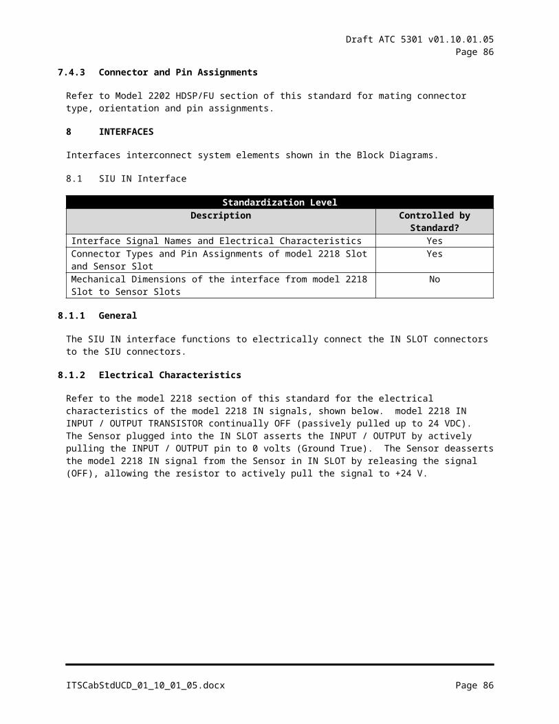
Draft ATC 5301 v01.10.01.05Page 86
Byte # Contents Description6: SIU-22187:255 Reserved
3:42 ASCII Text
A packed 40 character field describing the device properties. Allowable ASCII characters are 020h through 07Eh. If less than 40 characters are used, the unused locations shall be set to 00h. Default programming shall be 00h.
9.1.6 SIU2218 SB1 Frame Types
9.1.6.1Request Module Status
The command shall be used to request model 2218 status information response. Command/response frames shall be as follows:
Table 33: Request Module Status Command
Description msb lsb Byte Number(Type Number = 49) 0 0 1 1 0 0 0 1 Byte 1Reset Status Bits P E K R T M L W Byte 2
Table 34: Request Module Status Response
Description msb lsb Byte Number(Type Number = 177) 1 0 1 1 0 0 0 1 Byte 1System Status P E K R T M L W Byte 2SCC Receive Error Count Receive Error Count Byte 3SCC Transmit Error Count Transmit Error Count Byte 4MC Timestamp MSB MC Timestamp MSB Byte 5MC Timestamp NMSB MC Timestamp NMSB Byte 6MC Timestamp NLSB MC Timestamp NLSB Byte 7MC Timestamp LSB MC Timestamp LSB Byte 8
The response status bits are defined as follows:P - Indicates model 2218 hardware resetE - Indicates a communications loss of greater than two secondsM - Indicates an error with the Millisecond Counter interruptL - Indicates an error in the LINESYNCW - Indicates that the model 2218 has been reset by the WatchdogR - Indicates that the EIA-485 receive error count byte has rolled overT - Indicates that the EIA-485 transmit error count byte has rolled overK - Not Used
ITSCabStdUCD_01_10_01_05.docx Page 86
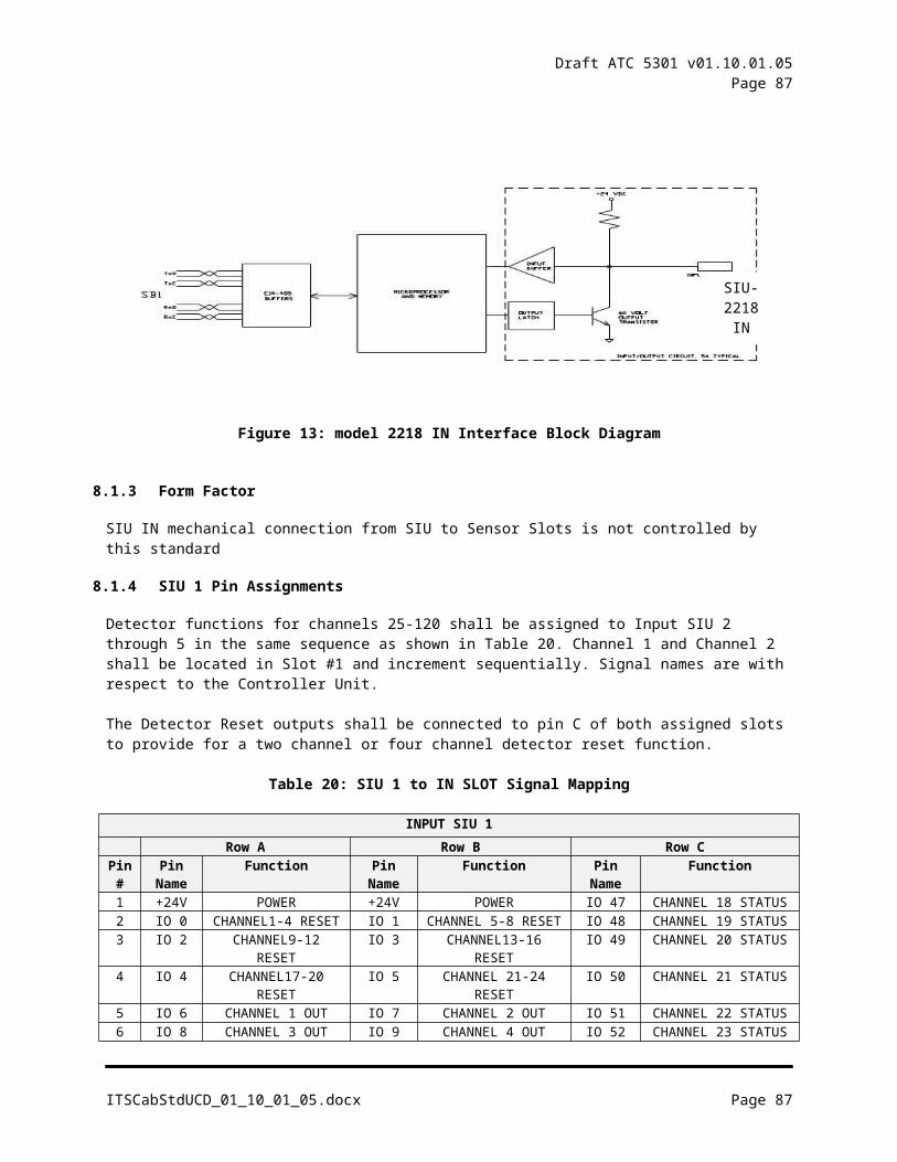
Draft ATC 5301 v01.10.01.05Page 87
Each of these bits shall be individually reset by a '1' in the corresponding bit of any subsequent Request Module Status frame, and the response frame shall report the current status bits. The SCC error count bytes shall not be reset. When a count rolls over (255 - 0), its corresponding roll-over flag shall be set.
9.1.6.2Millisecond Counter Management
The millisecond counter management frame shall be used to set the value of the millisecond counter. The 'S' bit shall return status '0' on completion or '1' on error. The 32-bit value shall be loaded into the millisecond counter at the next 0-1 transition of the LINESYNC signal. The frames shall be as follows:
Table 35: Millisecond Counter Management Command
Description msb lsb Byte Number(Type Number = 50) 0 0 1 1 0 0 1 0 Byte 1New MC Timestamp MSB x x x x x x x x Byte 2New MC Timestamp NMSB x x x x x x x x Byte 3New MC Timestamp NLSB x x x x x x x x Byte 4New MC Timestamp LSB x x x x x x x x Byte 5
Table 36: Millisecond Counter Management Response
Description msb lsb Byte Number(Type Number = 178) 1 0 1 1 0 0 1 0 Byte 1Status 0 0 0 0 0 0 0 S Byte 2
9.1.6.3Configure Inputs
The configure inputs command frame shall be used to change input configurations. The command-response frames shall be as follows:
Table 37: Configure Inputs Command
Description msb lsb Byte Number(Type Number = 51) 0 0 1 1 0 0 1 1 Byte 1Number of Items (n) n n n n n n n n Byte 2Item # - Byte 1 E Input Number (I0 – I59) Byte 3(I-1)+3Item # - Byte 2 Leading edge filter (e) Byte 3(I-1)+4Item # - Byte 3 Trailing edge filter (r) Byte 3(I-1)+5
Table 38: Configure Inputs Response
Description msb lsb Byte Number(Type Number = 179) 1 0 1 1 0 0 1 1 Byte 1
ITSCabStdUCD_01_10_01_05.docx Page 87
Draft ATC 5301 v01.10.01.05Page 88
Status 0 0 0 0 0 0 0 S Byte 2
Block field definitions shall be as follows:E - Ignore Input Flag. "1" = do not record transition entries for this input, "0" = record transition entries
for this inpute - A one-byte leading edge filter specifying the number of consecutive input samples which must be
"0" before the input is considered to have entered to "0" state from "1" state (range 1 to 255, 0 = filtering disabled)
r - A one-byte trailing edge filter specifying the number of consecutive input samples which must be "1" before the input is considered to have entered to "1" state from "0" state (range 1 to 255, 0 = filtering disabled)
S - return status S = '0' on completion or '1' on error
9.1.6.4Poll Raw Inputs Data
The poll raw input data frame shall be used to poll the model 2218 for the current unfiltered status of all inputs. The response frame shall contain 8 bytes (Inputs 0-63) of information indicating the current input status. The frames shall be as follows:
Table 39: Poll Raw Input Data
Description msb lsb Byte Number
(Type Number = 52) 0 0 1 1 0 1 0 0 Byte 1
Table 40: Poll Raw Data Response
Description msb lsb Byte Number
(Type Number = 180) 1 0 1 1 0 1 0 0 Byte 1Inputs I0 (lsb) to I7 (msb) x x x x x x x x Byte 2Inputs I8 to I54 x x x x x x x x Bytes 3 to 8Inputs I56 to I59, A0 to A3 A3 A2 A1 A0 I59 I58 I57 I56 Byte 9MC Timestamp MSB x x x x x x x x Byte 10MC Timestamp NMSB x x x x x x x x Byte 11MC Timestamp NLSB x x x x x x x x Byte 12MC Timestamp LSB x x x x x x x x Byte 13
9.1.6.5Poll Filtered Input Data
The poll filtered input data frame shall be used to poll the model 2218 for the current filtered status of all inputs. The response frame shall contain 8 bytes (Inputs 0-63) of information indicating the current filtered status of the inputs. Raw input data shall be provided in the response for inputs that are not configured for filtering. The frames shall be as follows:
ITSCabStdUCD_01_10_01_05.docx Page 88
Draft ATC 5301 v01.10.01.05Page 89
Table 41: Poll Filtered Data Command
Description msb lsb Byte Number(Type Number = 53) 0 0 1 1 0 1 0 1 Byte 1
Table 42: Poll Filtered Data Response
Description msb lsb Byte Number(Type Number = 181) 1 0 1 1 0 1 0 1 Byte 1Inputs I0 (lsb) to I7 (msb) x x x x x x x x Byte 2Inputs I8 to I53, I56 to I59 x x x x x x x x Bytes 3 to 9MC Timestamp MSB x x x x x x x x Byte 10MC Timestamp NMSB x x x x x x x x Byte 11MC Timestamp NLSB x x x x x x x x Byte 12MC Timestamp LSB x x x x x x x x Byte 13
9.1.6.6Poll Input Transition Buffer
The poll input transition buffer frame shall poll the model 2218 for the contents of the input transition buffer. The response frame shall include a three-byte information field for each of the input changes that have occurred since the last interrogation. The frames are as follows:
Table 43: Poll Input Transition Buffer Command
Description msb lsb Byte Number(Type Number = 54) 0 0 1 1 0 1 1 0 Byte 1Block Number x x x x x x x x Byte 2
Table 44: Poll Input Transition Buffer Response
Description msb lsb Byte Number
(Type Number = 182) 1 0 1 1 0 1 1 0 Byte 1Block Number x x x x x x x x Byte 2Number of Entries = N x x x x x x x x Byte 3Item # S Input Number (I0 – I59) Byte 3(I-1)+4Item # MC Timestamp NLSB x x x x x x x x Byte 3(I-1)+5Item # MC Timestamp LSB x x x x x x x x Byte 3(I-1)+6Status 0 0 0 0 C F E G Byte 3(I-1)+7MC Timestamp MSB x x x x x x x x Byte 3(N-1)+8MC Timestamp NMSB x x x x x x x x Byte 3(N-1)+9MC Timestamp NLSB x x x x x x x x Byte 3(N-1)+10MC Timestamp LSB x x x x x x x x Byte 3(N-1)+11
Each detected state transition for each active input (see 4.7.9 and 4.7.15.4) is placed in the queue as it occurs. Bit definitions are as follows:
ITSCabStdUCD_01_10_01_05.docx Page 89
Draft ATC 5301 v01.10.01.05Page 90
S - Indicates the state of the input after the transition, bit is 1 if the Input is ON after the transition, bit is 0 if the Input is OFF after the transition
C - Indicates the 255 entry buffer limit has been exceededF - Indicates the 1024 buffer limit has been exceededG - Indicates the requested block number is out of monotonic increment sequenceE - Same block number requested, E is set in response
The entries provided within the transition buffer poll response shall be ordered from the start of the reply as the oldest to newest. The very first access provides the oldest entry. The model 2218 device shall initialize, upon Power Up or Reset, its last block number received value to 0xFF in order to facilitate suppression of the G Bit response when the ATC program starts and uses 0x00 as the first block number. Subsequent responses are subject to the old-buffer purge mechanism stated below.
The ATC program monotonically increases the block number after each command issued to purge the old buffer. When the model 2218 module receives this command, it shall compare the associated block number with the block number of the previously received command. If it is the same, the previous buffer shall be re-sent to the ATC and the 'E' flag set in the status response frame. If it is not equal to the previous block number, the old buffer shall be purged and the next block of data sent. If the block number is not incremented by one, the status G bit shall be set. The block number received becomes the current number (even if out of sequence). The block number byte sent in the response block shall be the same as that received in the command block. The block number counter rollover (0xFF becomes 0x00) shall be considered as a normal increment.
9.1.6.7Set Outputs
The set outputs frame shall be used to command the model 2218 to set the outputs according to the data in the frame. If there is any error configuring the outputs, the 'E' flag in the response frame shall be set to '1'. If the LINESYNC reference has been lost, the 'L' bit in the response frame shall be set. Loss of LINESYNC reference shall also be indicated in system status information. These command and response frames are as follows:
Table 45: Set Outputs Command
Description msb lsb Byte Number
(Type Number = 55) 0 0 1 1 0 1 1 1 Byte 1
Outputs O0 (lsb) to O7 (msb) Data x x x x x x x x Byte 2
Outputs O8 to O54 Data x x x x x x x x Bytes 3 to 8
Outputs O56 to O63 Data (reserved) 0 0 0 0 0 0 0 0 Byte 9
Outputs O0 (lsb) to O7 (msb) Control x x x x x x x x Byte 10
Outputs O8 to O54 Control x x x x x x x x Bytes 11 to 16
Outputs O56 to O63 Control (reserved) 0 0 0 0 0 0 0 0 Byte 17
Table 46: Set Outputs Response
Description msb lsb Byte Number(Type Number = 183) 1 0 1 1 0 1 1 1 Byte 1Status 0 0 0 0 0 0 L E Byte 2
ITSCabStdUCD_01_10_01_05.docx Page 90
Draft ATC 5301 v01.10.01.05Page 91
9.1.6.8Configure Input Tracking Functions
The Configure Input Tracking Functions frame shall be used to configure the definition for an output that responds to transitions on a particular input. The maximum number of active definitions is 8.
Please note that Configure Input Tracking Functions is not intended for use with Traffic SignalControl Applications. (Authorized Engineering Information)
9.1.6.8.1Command and Response Frames
The command and response frames for Input Tracking Functions shall be as follows:
Table 47: Configure Input Tracking Function Command
Description msb lsb Byte Number(Type Number = 56) 0 0 1 1 1 0 0 0 Byte 1Number of Items Number of Items Byte 2Item # - Byte 1 E Output Number (O0 – O54) Byte 2(I-1)+3Item # - Byte 2 I Input Number (I0 – I59) Byte 2(I-1)+4
Number of Items: 0-16 Tracking Definitions are contained in this message.Field Definitions:
E '1’ - Enable Input Tracking function for this Output'0' - Remove Input Tracking function for this Output
I '1' - Output is OFF when Input is ON, ON when Input OFF'0' - Output is ON when Input is ON, OFF when Input is OFF
Output Number: 0 - Maximum Output Number for the model 2218 device type.Input Number: 0 - Maximum Input Number for the model 2218 device type.
Table 48: Configure Input Tracking Function Response
Description msb lsb Byte Number
(Type Number = 184) 1 0 1 1 1 0 0 0 Byte 1Status 0 0 0 0 0 0 0 V Byte 2MC Timestamp MSB x x x x x x x x Byte 3MC Timestamp NMSB x x x x x x x x Byte 4MC Timestamp NLSB x x x x x x x x Byte 5MC Timestamp LSB x x x x x x x x Byte 6
Field Definitions:
V '1' - Maximum number of configurable outputs will be exceeded.'0' - No error
9.1.6.8.2Timestamp
The timestamp value shall be sampled prior to the response frame.
ITSCabStdUCD_01_10_01_05.docx Page 91
Draft ATC 5301 v01.10.01.05Page 92
9.1.6.8.3Output Updates
Outputs, which track inputs, shall be updated no less than once per millisecond. Input to output signal propagation delay shall not exceed 2 milliseconds
9.1.6.8.4Tracking Functions Overview
A maximum of eight different output numbers may be activated by specifying eight definitions.
One complete definition for an output that tracks an Input consists of two bytes containing four parameters: 1) the instruction to install or to remove the definition, 2) the output number, 3) the relationship of the state of the output to the input and 4) the input number.
Each definition specifies the controlling input number for that unique output number. More than one output definition may specify the same input controlling source. [That is, the same input may be used as the control source for more than one tracking output.]
A complete definition is called an item in the command message frame. The ‘Number of Items’ byte specifies the quantity of complete definitions contained in the command frame. If the value is 0, all existing active input tracking definitions shall be removed.
The transmission of a definition may:a) Install a new active tracking definition.b) Remove an existing active tracking definition. When an input tracking definition is removed,
the output is set according to the most recently received set outputs command.c) Convert an active output definition from complex or square wave definition to tracking
conversion removes the existing definition and assigns the tracking definition without a transition through the ‘output is set according to the most recently received set outputs command’ state. The most recent state of the output remains until the new function changes it.
d) Redefine an existing tracking definition.
If a command frames to be processed by the model 2218 would result in having more than the maximum number (8) of definitions activated, the entire command frame shall be rejected. The response V bit shall be set to 1.
The V bit response is based on counting the current active quantity plus the projected enable definitions after accounting for remove definitions and invalid output numbers.
The V bit response evaluation takes the currently active definition quantity, adds the projected enable definitions, subtracts the remove definitions, ignores invalid input and output numbers and compares the result to the maximum number of active tracking definitions allowed. If the quantity of active definitions would become greater than the maximum number of active tracking definitions, or if there are more remove definitions than existing active definitions, the V bit shall be set in the response.
While processing an enable request, an out of range input number shall preclude processing for that definition.
The out of range output and input numbers shall not affect the active definition count. No error response is returned.
The rest of the message shall be processed.
The “Number of Items” field is valid from 0 to 16 because the longest message may contain 8 Enable and 8 Remove definitions.
ITSCabStdUCD_01_10_01_05.docx Page 92
Draft ATC 5301 v01.10.01.05Page 93
The input state always comes from the filtered input data source.
Valid Input and Output Number Ranges:model 2218 device types: Inputs 0 - 53 & 56 - 59, Outputs 0 - 54
9.1.6.9Configure Complex Output Functions
The Configure Complex Output Functions frame shall be used to configure the definition for an output that provides a complex operation. The maximum number of active definitions is 8.
Please note that Configure Complex Output Functions is not intended for use with Traffic Signal Control Applications. (Authorized Engineering Information)
9.1.6.9.1Command and Response Frames
The command and response frames shall be as follows:
Table 49: Configure Complex Outputs
Description msb lsb Byte Number
(Type Number = 57) 0 0 1 1 1 0 0 1 Byte 1Number of Items Number of Items Byte 2Item # - Byte 1 0 Output Number (O0 – O54) Byte 7(I-1)+3Item # - Byte 2 Primary Duration (MSB) Byte 7(I-1)+4Item # - Byte 3 Primary Duration (LSB) Byte 7(I-1)+5Item # - Byte 4 Secondary Duration (MSB) Byte 7(I-1)+6Item # - Byte 5 Secondary Duration (LSB) Byte 7(I-1)+7Item # - Byte 6 0 Input Number (I0 – I59) Byte 7(I-1)+8Item # - Byte 7 P W G E J F R L Byte 7(I-1)+9
Number of Items: 0-16 Complex Output Definitions are contained in this message.Output Number: 0 - Maximum Output Number for the model 2218 device type.Primary Duration: MSB & LSB form a 16 bit Hex numerical value 0x0000 - 0xffff.Secondary Duration: MSB & LSB form a 16 bit Hex numerical value 0x0000 - 0xffff.Input Number: 0 - Maximum Input Number for the model 2218 device type.
Field Definitions:P '1' - The output is configured for single-pulse operation.
Once complete, the complex output function shall be disabled.'0' - The output is configured for continuous oscillation.
W '1' - It is triggered by the specified input.Triggered complex output shall commence within 2 milliseconds of the associated trigger recognition.
'0' - Operation shall begin within two milliseconds of the command receipt.G '1' - Operation shall be gated active by the specified input.
'0' - Gating is inactive.E '1' Enable complex output function for this output
'0' Remove complex output function for this outputJ '1' During primary duration, the output shall be written as a logic '1'.
During secondary duration, the output shall be written as a logic '0'.'0' During primary duration, the output shall be written as a logic '0'.
During secondary duration, the output shall be written as a logic '1'
ITSCabStdUCD_01_10_01_05.docx Page 93
Draft ATC 5301 v01.10.01.05Page 94
F '1' - The trigger or gate shall be acquired subsequent to filtering the specified input.The raw input signal shall be used if filtering is not enabled for the specified input.
'0' - The trigger or gate shall be derived from the raw input.R '1' - For triggered output, the output shall be triggered by an ON-to-OFF transition of the
………..specified input and shall be triggered immediately upon command receipt if the input is ………..OFF.
For gated output, the output shall be active while the input is OFF.'0' - For triggered output, the output shall be triggered by an OFF-to-ON transition of the
specified input and shall be triggered immediately upon command receipt if the input is ON. For gated output, the output shall be active while the input is ON.
L '1' – The LINESYNC based clock shall be used for the time ticks.'0' - The millisecond counter shall be used for the time ticks.
Table 50: Configure Complex Output Functions Response
Description msb lsb Byte Number
(Type Number = 57) 0 0 1 1 1 0 0 1 Byte 1Number of Items Number of Items Byte 2Item # - Byte 1 0 Output Number (O0 – O54) Byte 7(I-1)+3Item # - Byte 2 Primary Duration (MSB) Byte 7(I-1)+4Item # - Byte 3 Primary Duration (LSB) Byte 7(I-1)+5Item # - Byte 4 Secondary Duration (MSB) Byte 7(I-1)+6Item # - Byte 5 Secondary Duration (LSB) Byte 7(I-1)+7Item # - Byte 6 0 Input Number (I0 – I59) Byte 7(I-1)+8Item # - Byte 7 P W G E J F R L Byte 7(I-1)+9
Field Definitions:
V '1' - Maximum number of configurable outputs will be exceeded. '0' - No error
9.1.6.9.2Sampling Rate
Controlling input signals shall be sampled at least once per millisecond.
9.1.6.9.3Complex Output Functions Overview
A maximum of eight different output numbers may be activated by specifying eight definitions. One complete definition for a complex output consists of seven bytes containing fourteen parameters:1) The Output Number,2, 3) Primary Duration: MSB & LSB form a 16 bit Hex numerical value,4, 5) Secondary Duration: MSB & LSB form a 16 bit Hex numerical value,6) The Input Number,7) Bit P: One Pulse or Continuous Oscillation,8) Bit W: Output Operation is Edge Triggered by Input or Not Triggered by Input,9) Bit G: Output Operation is Gated by Input or is Continuous Oscillation,10) Bit E: Enable Definition or Remove Definition,11) Bit J: Defines Primary/Secondary Duration relationship: ON/OFF or OFF/ON,12) Bit F: Input from Filtered or Raw Data,13) Bit R: Selects Edge for Triggered by Input ON to OFF or OFF to ON. Bit R: Selects State for
Gated to be active by Input OFF or by Input ON,14) Linesync edges or millisecond counter provides tick timing.
ITSCabStdUCD_01_10_01_05.docx Page 94

Draft ATC 5301 v01.10.01.05Page 95
Each definition specifies the controlling Input number for that unique output number. The input is a functional control only when the operation is specified as Triggered (W=1) or Gated (G=1). Otherwise, the input number is ignored. More than one output definition may specify the same Input controlling source. [That is, the same input may be used as the control source for more than one complex output.] If both W=1 and G=1 are set in the definition, the G=1 shall be used as if W=0.
The primary duration is the first timed interval of a pulse or the first portion of a continuous oscillation. The first portion follows acquisition of a trigger or gated input. If not triggered or gated, the first portion follows the activation of the definition.
The secondary duration follows the primary duration.
A complete definition is called an item in the command message frame.
The ‘Number of Items’ byte specifies the quantity of complete definitions contained in the command frame. If the value is 0, all existing active complex output definitions shall be removed.
The transmission of a definition may:
a) Install a new active complex output definition.b) Remove an existing active complex output definition. When a complex output definition is
removed, the output is set according to the most recently received set outputs command.c) Convert an active output definition from tracking or square wave definition to complex output.
Conversion removes the existing definition and assigns the complex output definition without a transition through the ‘output is set according to the most recently received Set Outputs Command’ state. The most recent state of the output remains until the new function changes it.
d) Redefine an existing complex output definition.
If a command frame to be processed by the model 2218 would result in having more than the maximum number (8) definitions activated, the entire command frame shall be rejected. The response V bit shall be set to 1.
The V bit response evaluation takes the currently active definition quantity, adds the projected enable definitions, subtracts the remove definitions, ignores invalid input and output numbers and compares the result to the maximum number of active complex definitions allowed. If the quantity of active definitions would become greater than the maximum number of active complex output definitions, or if there are more Remove definitions than existing active complex output definitions, the V bit shall be set in the response.
While processing an Enable request that requires triggered or gated operation, an out of range input number shall preclude processing for that definition.
The out of range output and input numbers shall not affect the active definition count. No error response is returned.
The rest of the message shall be processed.
The “Number of Items” field is valid from 0 to 16 because the longest message may contain 8 enable and 8 remove definitions.
The input state comes from the filtered or raw input data source as specified by the bit F value.
Valid Input and Output Number Ranges:model 2218 device types: Inputs 0 - 53 & 56 - 59, Outputs 0 - 54
ITSCabStdUCD_01_10_01_05.docx Page 95
Draft ATC 5301 v01.10.01.05Page 96
The LINESYNC based clock shall used both the rising and falling edges providing a nominal 8.33 millisecond time tick.
9.1.7 CMU2212 SB1 Frame Types
9.1.7.1Type 80 Command – Module Description
Table 51: Serial Bus #1 Type 80 Command
Byte # Contents Description1 80 Frame Type
9.1.7.2Type 208 Response – Module Description
Table 52: Serial Bus #1 Type 208 Response
Byte # Contents Description1 208 Frame Type
2 Device
Enumerated Device Type1: CMU-2122: CMU-2212-LV3: CMU-2212-HV4: CMU-2212-VHV (Reserved)5: SIU-2186: model 22187:255 Reserved
3:42 ASCII Text
A packed 40 character field describing the device properties. Allowable ASCII characters are 020h through 07Eh. If less than 40 characters are used, the unused locations shall be set to 00h. Default programming shall be 00h.
9.1.7.3Type 81 Command – Switch Pack Drivers
The destination for this frame shall be the CMU. The channel numbers in the description column below refer to the channel numbers of the CMU. The ATC shall include a definition, via program entry, of the CMU channel to ATC signal driver group utilization. The Dark Channel Map Select bits shall select a preprogrammed mask in the CMU serial memory key that disables Lack of Signal Input monitoring for the selected channels.
Table 53: Serial Bus #1 Type 81 Command
Byte # Contents Description
1 81 Frame Type2 Channel 8:1 Red HDSP Status
A bit set to 1 indicates the HDSP output is set ON.3 Channel 16:9 Red4 Channel 24:17 Red
ITSCabStdUCD_01_10_01_05.docx Page 96
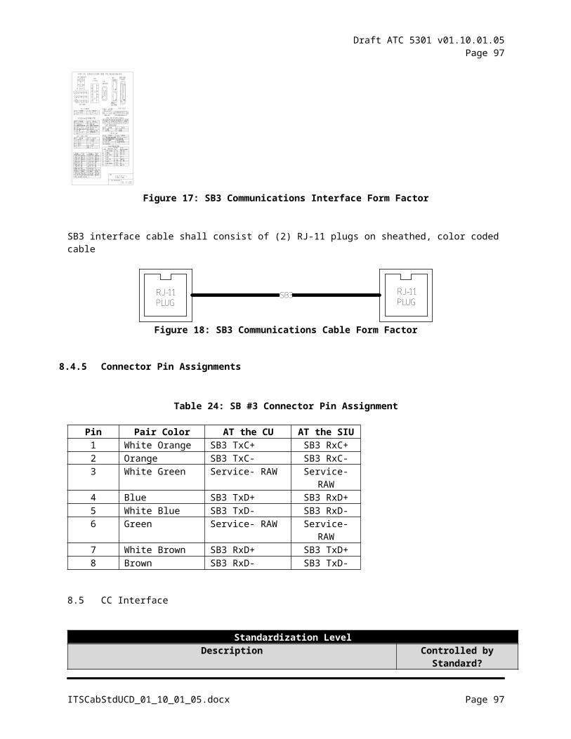
Draft ATC 5301 v01.10.01.05Page 97
Byte # Contents Description5 Channel 32:25 Red6 Channel 8:1 Yellow7 Channel 16:9 Yellow8 Channel 24:17 Yellow9 Channel 32:25 Yellow
10 Channel 8:1 Green11 Channel 16:9 Green12 Channel 24:17 Green13 Channel 32:25 Green14 Map Select Dark Channel Map Select
Bit 1 and bit 0 shall select one of four Dark Channel Maps programmed in the serial memory key that disables Lack of Signal Input monitoring for a selected channel. 00 = Mask #101 = Mask #210 = Mask #311 = Mask #4Bits 2 thru 7 are Reserved
9.1.7.4Type 81 Response – CMU Status
If the CMU is in FSA (byte #2, Fault Type not equal to 0), then all bytes of the information field of this frame except Control Status 1, Control Status 2 and Output Assembly Flasher Status shall contain an exact image of the signals that were applied to the CMU at the point in time of the detection of the failure. Control Status 1, Control Status 2 and Output Assembly Flasher Status shall always reflect current status.
Table 54: Serial Bus #1 Type 81 Response
Byte # Contents Description
1 209 Frame Type2 Fault Type Enumerated fault code
00 = No Fault01 = CMU/HDSP +24 VDC02 = CMU +12 VDC03 = Conflict04 = Serial Bus #105 = Serial Bus #306 = ATC LFSA Flash (Type 62)07 = ATC NFSA Flash (Type 62)08 = Diagnostic09 = Multiple10 = Lack of Signal Input11 = Short Yellow Clearance12 = Skipped Yellow Clearance13 = Yellow + Red Clearance14 = Field Output Check
ITSCabStdUCD_01_10_01_05.docx Page 97
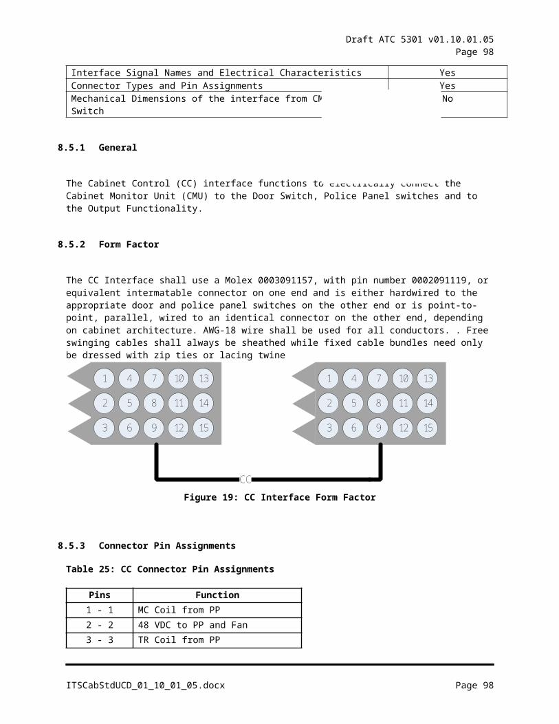
Draft ATC 5301 v01.10.01.05Page 98
Byte # Contents Description15 = Serial Memory Key absent16 = Serial Memory Key FCS error 17 = Serial Memory Key Data error18 = Local Flash19 = CB Trip20 = CMU/HDSP Mains Fail21 = NRESET Active22 = HDSP Diagnostic23 = FYA Flash Rate Fault24:127 = Reserved128:255 = Spare (Resrved for Mfg Use)
3 Channel Fault Status 8:1 Channel Fault Status Channel Fault Status bits shall be set to 1 for channels that were detected in fault for fault types 03, 09, 10, 11, 12, 13, and 14.
For fault type 01, 05, and 20 a bit shall be set in Channel Fault Status 32:1 for each enabled HDSP channel that failed. For type 01, if the 24VDC input failed then Channel Fault Status shall be set to 0. For type 20, if the CMU MAINS input failed then Channel Fault Status shall be set to 0.
For all other fault types the Channel Fault Status bits shall be set to 0.
4 Channel Fault Status 16:95 Channel Fault Status 24:176 Channel Fault Status 32:25
7 Channel Red Status 8:1 Channel Color Status Channel Color Status bits shall be set to 1 for channels that are sensed active. For channel inputs that have been remapped to a virtual channel (29-32), the Channel Fault Status bits shall be set to 0. For virtual channel (29-32) inputs that have not been assigned to a physical output, the Channel Fault Status bits shall be set to 0.
8 Channel Red Status 16:99 Channel Red Status 24:17
10 Channel Red Status 32:2511 Channel Yellow Status 8:112 Channel Yellow Status 16:913 Channel Yellow Status 24:1714 Channel Yellow Status 32:2515 Channel Green Status 8:116 Channel Green Status 16:917 Channel Green Status 24:1718 Channel Green Status 32:2519 Channel Red Status 8:1 Field Check Status
Field Check Status bits shall be set to 1 for channels that are sensed with field check status. For channel inputs that have been remapped to a virtual channel (29-32), the Field Check Status bits shall be set to 0. For virtual channel (29-32) inputs that have not been assigned to a physical output, the Field Check Status bits shall be set to 0.
20 Channel Red Status 16:921 Channel Red Status 24:1722 Channel Red Status 32:2523 Channel Yellow Status 8:124 Channel Yellow Status 16:925 Channel Yellow Status 24:1726 Channel Yellow Status 32:2527 Channel Green Status 8:1
ITSCabStdUCD_01_10_01_05.docx Page 98
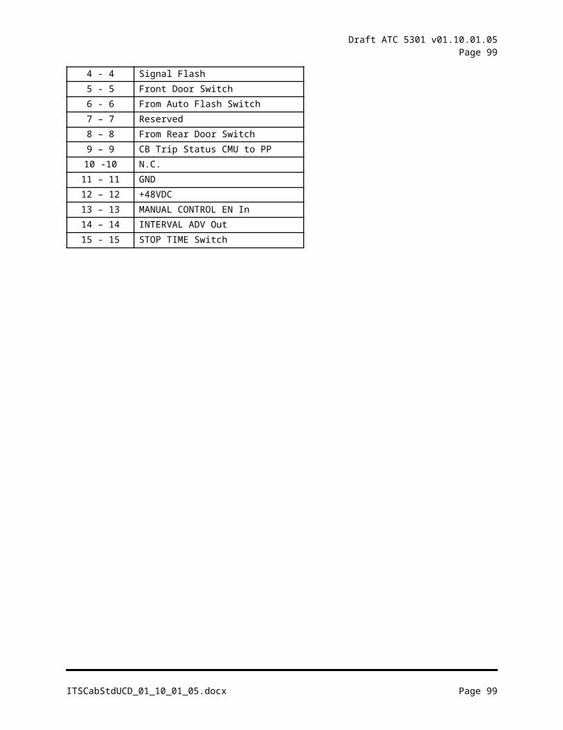
Draft ATC 5301 v01.10.01.05Page 99
Byte # Contents Description28 Channel Green Status 16:929 Channel Green Status 24:1730 Channel Green Status 32:2531 Control Status #1 Control Status #1
b7 = Start-up Call (1=Exit from Flash)b6 = Flasher Output Fail (1 = Fail)b5 = Rear Door (1=Open) b4 = Front Door (1=Open)b3 = MAIN CONTACTOR Coil (1=Active)b2 = MAIN CONTACTOR Secondary (1=Active)b1 = FTR Coil Drive (1= Active)b0 = Output Relay Transfer (1=Fault)
32 Control Status #2 Control Status #2b7 = Reservedb6 = Reservedb5 = Reservedb4 = Reservedb3 = Reservedb2 = Reservedb1 = Reservedb0 = Configuration Change
This bit set to 1 indicates the configuration programming has changed since the last poll of frame Type 82. It shall also be set to 1 when the CMU is exiting flash (Start-up Call bit changes from 0 to 1) and at CMU power-up.
33 Mains Raw Voltage CMU Mains Voltage34 Assembly #1 Signal Power
VoltageHDSP Signal Voltage
Signal Voltage for any HDSP in assembly #1 (channels 1:16)Signal Voltage for any HDSP in assembly #2 (channels 17:32)
35 Assembly #2 Signal Power Voltage
36 Channel 1 Red Voltage Channel Input Voltages The Channel input voltages shall be the most recent values reported from the HDSPs. For channel inputs that have been remapped to a virtual channel (29-32), the Channel Voltage value shall be set to 0.
The value for voltage shall be programmed in scaled volts.
37 Channel 2 Red Voltage38 Channel 3 Red Voltage39 Channel 4 Red Voltage40 Channel 5 Red Voltage41 Channel 6 Red Voltage42 Channel 7 Red Voltage43 Channel 8 Red Voltage44 Channel 9 Red Voltage45 Channel 10 Red Voltage46 Channel 11 Red Voltage47 Channel 12 Red Voltage48 Channel 13 Red Voltage
ITSCabStdUCD_01_10_01_05.docx Page 99
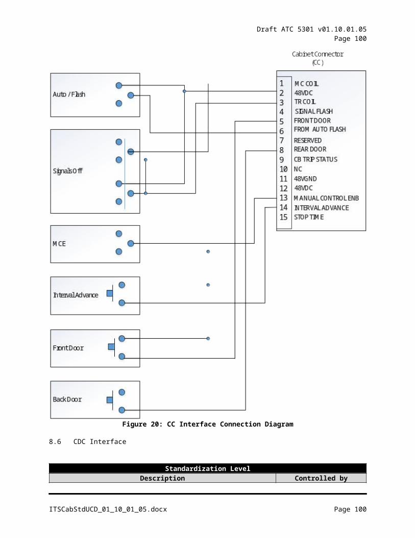
Draft ATC 5301 v01.10.01.05Page 100
Byte # Contents Description49 Channel 14 Red Voltage50 Channel 15 Red Voltage51 Channel 16 Red Voltage52 Channel 17 Red Voltage53 Channel 18 Red Voltage54 Channel 19 Red Voltage55 Channel 20 Red Voltage56 Channel 21 Red Voltage57 Channel 22 Red Voltage58 Channel 23 Red Voltage59 Channel 24 Red Voltage60 Channel 25 Red Voltage61 Channel 26 Red Voltage62 Channel 27 Red Voltage63 Channel 28 Red Voltage64 Channel 29 Red Voltage65 Channel 30 Red Voltage66 Channel 31 Red Voltage67 Channel 32 Red Voltage68 Channel 1 Yellow Voltage69 Channel 2 Yellow Voltage70 Channel 3 Yellow Voltage71 Channel 4 Yellow Voltage72 Channel 5 Yellow Voltage73 Channel 6 Yellow Voltage74 Channel 7 Yellow Voltage75 Channel 8 Yellow Voltage76 Channel 9 Yellow Voltage77 Channel 10 Yellow Voltage78 Channel 11 Yellow Voltage79 Channel 12 Yellow Voltage80 Channel 13 Yellow Voltage81 Channel 14 Yellow Voltage82 Channel 15 Yellow Voltage83 Channel 16 Yellow Voltage84 Channel 17 Yellow Voltage85 Channel 18 Yellow Voltage86 Channel 19 Yellow Voltage87 Channel 20 Yellow Voltage88 Channel 21 Yellow Voltage89 Channel 22 Yellow Voltage90 Channel 23 Yellow Voltage91 Channel 24 Yellow Voltage92 Channel 25 Yellow Voltage93 Channel 26 Yellow Voltage
ITSCabStdUCD_01_10_01_05.docx Page 100
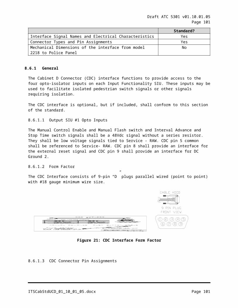
Draft ATC 5301 v01.10.01.05Page 101
Byte # Contents Description94 Channel 27 Yellow Voltage95 Channel 28 Yellow Voltage96 Channel 29 Yellow Voltage97 Channel 30 Yellow Voltage98 Channel 31 Yellow Voltage99 Channel 32 Yellow Voltage
100 Channel 1 Green Voltage101 Channel 2 Green Voltage102 Channel 3 Green Voltage103 Channel 4 Green Voltage104 Channel 5 Green Voltage105 Channel 6 Green Voltage106 Channel 7 Green Voltage107 Channel 8 Green Voltage108 Channel 9 Green Voltage109 Channel 10 Green Voltage110 Channel 11 Green Voltage111 Channel 12 Green Voltage112 Channel 13 Green Voltage113 Channel 14 Green Voltage114 Channel 15 Green Voltage115 Channel 16 Green Voltage116 Channel 17 Green Voltage117 Channel 18 Green Voltage118 Channel 19 Green Voltage119 Channel 20 Green Voltage120 Channel 21 Green Voltage121 Channel 22 Green Voltage122 Channel 23 Green Voltage123 Channel 24 Green Voltage124 Channel 25 Green Voltage125 Channel 26 Green Voltage126 Channel 27 Green Voltage127 Channel 28 Green Voltage128 Channel 29 Green Voltage129 Channel 30 Green Voltage130 Channel 31 Green Voltage131 Channel 32 Green Voltage132 Channel 1 Red Current Scaled Load Current
The output load current values for current sense shall be programmed in scaled milliamps. IF Param >120
Then Current = (Param *16) – 1800Else Current = Param
133 Channel 2 Red Current134 Channel 3 Red Current135 Channel 4 Red Current136 Channel 5 Red Current137 Channel 6 Red Current138 Channel 7 Red Current
ITSCabStdUCD_01_10_01_05.docx Page 101
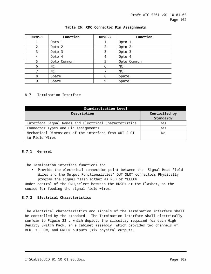
Draft ATC 5301 v01.10.01.05Page 102
Byte # Contents DescriptionIf Param > 250 Then Current = “> 2200” mA139 Channel 8 Red Current
140 Channel 9 Red Current141 Channel 10 Red Current142 Channel 11 Red Current143 Channel 12 Red Current144 Channel 13 Red Current145 Channel 14 Red Current146 Channel 15 Red Current147 Channel 16 Red Current148 Channel 17 Red Current149 Channel 18 Red Current150 Channel 19 Red Current151 Channel 20 Red Current152 Channel 21 Red Current153 Channel 22 Red Current154 Channel 23 Red Current155 Channel 24 Red Current156 Channel 25 Red Current157 Channel 26 Red Current158 Channel 27 Red Current159 Channel 28 Red Current160 Channel 29 Red Current161 Channel 30 Red Current162 Channel 31 Red Current163 Channel 32 Red Current164 Channel 1 Yellow Current165 Channel 2 Yellow Current166 Channel 3 Yellow Current167 Channel 4 Yellow Current168 Channel 5 Yellow Current169 Channel 6 Yellow Current170 Channel 7 Yellow Current171 Channel 8 Yellow Current172 Channel 9 Yellow Current173 Channel 10 Yellow Current174 Channel 11 Yellow Current175 Channel 12 Yellow Current176 Channel 13 Yellow Current177 Channel 14 Yellow Current178 Channel 15 Yellow Current179 Channel 16 Yellow Current180 Channel 17 Yellow Current181 Channel 18 Yellow Current182 Channel 19 Yellow Current183 Channel 20 Yellow Current
ITSCabStdUCD_01_10_01_05.docx Page 102

Draft ATC 5301 v01.10.01.05Page 103
Byte # Contents Description184 Channel 21 Yellow Current185 Channel 22 Yellow Current186 Channel 23 Yellow Current187 Channel 24 Yellow Current188 Channel 25 Yellow Current189 Channel 26 Yellow Current190 Channel 27 Yellow Current191 Channel 28 Yellow Current192 Channel 29 Yellow Current193 Channel 30 Yellow Current194 Channel 31 Yellow Current195 Channel 32 Yellow Current196 Channel 1 Green Current197 Channel 2 Green Current198 Channel 3 Green Current199 Channel 4 Green Current200 Channel 5 Green Current201 Channel 6 Green Current202 Channel 7 Green Current203 Channel 8 Green Current204 Channel 9 Green Current205 Channel 10 Green Current206 Channel 11 Green Current207 Channel 12 Green Current208 Channel 13 Green Current209 Channel 14 Green Current210 Channel 15 Green Current211 Channel 16 Green Current212 Channel 17 Green Current213 Channel 18 Green Current214 Channel 19 Green Current215 Channel 20 Green Current216 Channel 21 Green Current217 Channel 22 Green Current218 Channel 23 Green Current219 Channel 24 Green Current220 Channel 25 Green Current221 Channel 26 Green Current222 Channel 27 Green Current223 Channel 28 Green Current224 Channel 29 Green Current225 Channel 30 Green Current226 Channel 31 Green Current227 Channel 32 Green Current228 Binary Seconds CMU Time and Date
ITSCabStdUCD_01_10_01_05.docx Page 103
Draft ATC 5301 v01.10.01.05Page 104
Byte # Contents Description229 Binary Minutes230 Binary Hours (0:23)231 Binary Date232 Binary Month233 Binary Year234 Voltage * 4 24 VDC Supply Voltage235 Voltage * 8 12 VDC Supply Voltage236 degrees F + 40 CMU Temperature (Fahrenheit)237 Red Status 8:1 Channel Current Sense Status
Status bits shall be set to 1 for channels that are sensed active. Status bits shall be set to 0 for channels that have the Current Sense monitor function disabled.
238 Red Status 16:9239 Red Status 24:17240 Red Status 32:25241 Yellow Status 8:1242 Yellow Status 16:9243 Yellow Status 24:17244 Yellow Status 32:25245 Green Status 8:1246 Green Status 16:9247 Green Status 24:17248 Green Status 32:25249 Assembly 2:1 Flasher Status (1=Fail)
b0 = HDFU #1 FL1-1b1 = HDFU #1 FL1-2b2 = HDFU #1 FL2-1b3 = HDFU #1 FL2-2b4 = HDFU #2 FL1-1b5 = HDFU #2 FL1-2b6 = HDFU #2 FL2-1b7 = HDFU #2 FL2-2
9.1.7.5Type 62 – Send to Local Flash Command – SET FSA
Table 55 Type 62 Command
Byte # Contents Description
1 62 Frame Type2 FSA mode Set Failed State Action
b0 = Set LFSA (L)b1 = Set NFSA (N)b2:7 = reserved
9.1.7.6Type 190 Response – Send to Local Flash Response – Set FSA
Table 56: Type 190 Response
ITSCabStdUCD_01_10_01_05.docx Page 104
Draft ATC 5301 v01.10.01.05Page 105
Byte # Contents Description1 190 Frame Type
9.1.7.7Type 82 Command – Get CMU Configuration
The ATC shall request the serial memory key programming using this message and validate that the CMU permissive program settings are equal or less permissive than the ATC controller unit programming, and that the HDSP configuration programming is consistent with Output Assembly model 2218 assignment. If these checks are not validated, then the ATC shall issue a Type 62 frame with the L bit set causing a LFSA in the CMU. This check shall be performed at initialization and when the Type 209 or Type 195 Control Status 2, Configuration Change bit is set to 1.
Table 57: CMU Type 82 Command
Byte # Contents Description1 82 Frame Type
9.1.7.8Type 210 Response – CMU Configuration
Table 58: CMU Type 210 Response
Byte # Contents Description
1 210 Frame Type2:513 Bytes #1 thru #512 Serial Memory Key Contents
9.1.7.9Type 67 Command – Switch Pack Drivers
The format of this command frame shall be identical to Message 81 but requests a short status response from the CMU. This frame may be used as an alternate to Message 81. The destination for this frame shall be the CMU. The channel numbers in the description column below refer to the channel numbers of the CMU. The ATC shall include a definition, via program entry, of the CMU channel to ATC signal driver group utilization. The Dark Channel Map Select bits shall select a preprogrammed mask in the CMU serial memory key that disables Lack of Signal Input monitoring for the selected channels.
Table 59: CMU Type 67 Command
Byte # Contents Description
1 67 Frame Type
2 Channel 8:1 Red Switch Pack StatusA bit set to 1 indicates the HDSP output is set ON.3 Channel 16:9 Red
4 Channel 24:17 Red5 Channel 32:25 Red6 Channel 8:1 Yellow7 Channel 16:9 Yellow8 Channel 24:17 Yellow
ITSCabStdUCD_01_10_01_05.docx Page 105
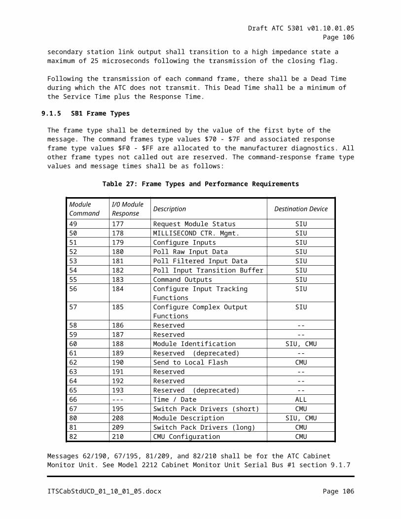
Draft ATC 5301 v01.10.01.05Page 106
Byte # Contents Description
9 Channel 32:25 Yellow10 Channel 8:1 Green11 Channel 16:9 Green12 Channel 24:17 Green13 Channel 32:25 Green14 Map Select Dark Channel Map Select
Bit 1 and bit 0 shall select one of four Dark Channel Maps programmed in the serial memory key that disables Lack of Signal Input monitoring for a selected channel. Bits 2 thru 7 are reserved.
00 = Mask #101 = Mask #210 = Mask #311 = Mask #4
9.1.7.10 Type 195 Response – CMU Short Status
If the CMU is in FSA (byte #2, Fault Type not equal to 0), then the channel color status bytes shall contain an exact image of the signals that were applied to the CMU at the point in time of the detection of the failure. Control Status 1, Control Status 2 and Output Assembly Flasher Status shall always reflect current status.
Table 60: CMU Type 195 Response
Byte # Contents Description
1 195 Frame Type2 Fault Type Enumerated fault code
00 = No Fault01 = CMU/HDSP +24 VDC02 = CMU +12 VDC03 = Conflict04 = Serial Bus #105 = Serial Bus #306 = ATC LFSA Flash (Type 62)07 = ATC NFSA Flash (Type 62)08 = Diagnostic09 = Multiple10 = Lack of Signal Input11 = Short Yellow Clearance12 = Skipped Yellow Clearance13 = Yellow + Red Clearance14 = Field Output Check15 = Serial Memory Key absent16 = Serial Memory Key FCS error 17 = Serial Memory Key Data error18 = Local Flash
ITSCabStdUCD_01_10_01_05.docx Page 106

Draft ATC 5301 v01.10.01.05Page 107
Byte # Contents Description
19 = CB Trip20 = CMU/HDSP Mains Fail21 = NRESET Active22 = HDSP Diagnostic23 = FYA Flash Rate Fault24:127 = Reserved128:255 = Spare (Reserved for Mfg Use)
3 Channel Fault Status 8:1 Channel Fault Status Channel Fault Status bits shall be set to 1 for channels that were detected in fault for fault types 03, 09, 10, 11, 12, 13, and 14.
For fault type 01, 05, and 20 a bit shall be set in Channel Fault Status 32:1 for each enabled HDSP channel that failed. For type 01, if the 24VDC input failed then Channel Fault Status shall be set to 0. For type 20, if the CMU MAINS input failed then Channel Fault Status shall be set to 0.
For all other fault types the Channel Fault Status bits shall be set to 0.
4 Channel Fault Status 16:95 Channel Fault Status 24:176 Channel Fault Status 32:25
7 Channel Red Status 8:1 Channel Color Status Channel Color Status bits shall be set to 1 for channels that are sensed active. For channel inputs that have been remapped to a virtual channel (29-32), the Channel Fault Status bits shall be set to 0. For virtual channel (29-32) inputs that have not been assigned to a physical output, the Channel Fault Status bits shall be set to 0.
8 Channel Red Status 16:99 Channel Red Status 24:17
10 Channel Red Status 32:2511 Channel Yellow Status 8:112 Channel Yellow Status 16:913 Channel Yellow Status 24:1714 Channel Yellow Status 32:2515 Channel Green Status 8:116 Channel Green Status 16:917 Channel Green Status 24:1718 Channel Green Status 32:2519 Control Status #1 Control Status #1
b7 = Start-up Call (1=Exit from Flash)b6 = Flasher Output Fail (1 = Fail)b5 = Rear Door (1=Open) b4 = Front Door (1=Open)b3 = MAIN CONTACTOR Coil (1=Active)b2 = MAIN CONTACTOR Secondary (1=Active)b1 = FTR Coil Drive (1= Active)b0 = Output Relay Transfer (1=Fault)
20 Control Status #2 Control Status #2b7 = Reservedb6 = Reservedb5 = Reserved
ITSCabStdUCD_01_10_01_05.docx Page 107
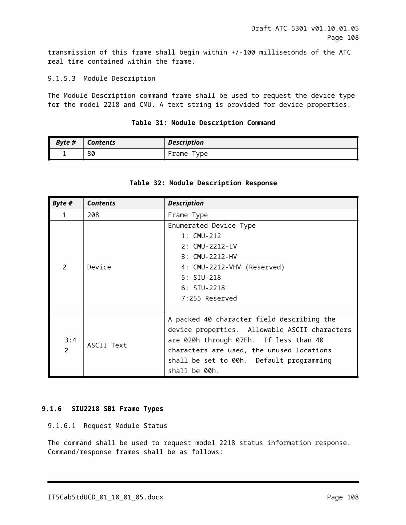
Draft ATC 5301 v01.10.01.05Page 108
Byte # Contents Description
b4 = Reservedb3 = Reservedb2 = Reservedb1 = Reservedb0 = Configuration Change
This bit set to 1 indicates the configuration programming has changed since the last poll of frame Type 82. It shall also be set to 1 when the CMU is exiting flash (Start-up Call bit changes from 0 to 1) and at CMU power-up.
21 Assembly 2:1 Flasher Status (1=Fail)b0 = HDFU #1 FL1-1b1 = HDFU #1 FL1-2b2 = HDFU #1 FL2-1b3 = HDFU #1 FL2-2b4 = HDFU #2 FL1-1b5 = HDFU #2 FL1-2b6 = HDFU #2 FL2-1b7 = HDFU #2 FL2-2
22 Assembly 4:3
23 Reserved24 Reserved
9.2 SB2 Communications Protocol
9.2.1 General
Serial bus #2 (SB2) shall be dedicated to gathering preprocessed data from the Cabinet Smart Input Devices resident in the input assemblies. SB2 connects in parallel with C12S of the ATC 5201 Controller Unit and one or more SIUs. Each model 2218 buffers SB2 to one or more sensor devices. This serial bus shall be for ATC data collection such as sensor operational status, detection speed reports, occupancy reports, vehicle counts, etc.
9.2.2 Data Link Layer
Serial bus #2 shall be designed to operate Asynchronous (1) START BIT Programmable number of DATA BITS (1) or (2) STOP BIT(s) Optional PARITY BIT Selectable data rates up to 19,200 bits per second.
9.2.3 Communication Frames
Typical Command/Response Messages shall use similar message format as Serial Bus #1. The Commands and Responses are not controlled by this standard, but correspond to the input devices used. For example, the protocol software driver for a certain input device type shall be installed into the ATC 5201 controller for execution. Refer to ATC 5201 standard for SB2 port configuration and operation.
ITSCabStdUCD_01_10_01_05.docx Page 108
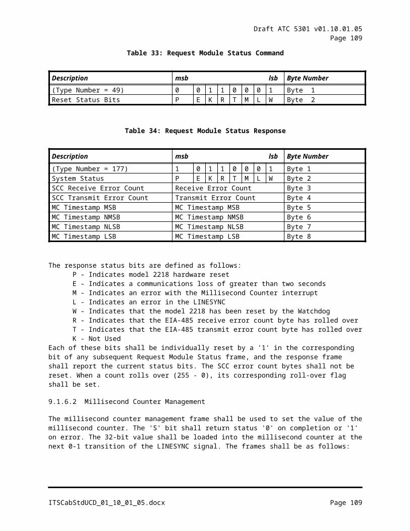
Draft ATC 5301 v01.10.01.05Page 109
9.3 SB3 Communications Protocol
9.3.1 General
Serial Bus #3 is used by the CMU2212 to communicate with the 2202 HDSP/FU and the model 2220.
9.3.2 Serial Bus Terminations
No termination loads shall be provided by the 2202 HDSP/FU. Serial Bus #3 termination is provided by the CMU2212 (RXD) and the model 2220 (TXD). The model 2220 shall provide the electrical termination for the SB #3 RxD inputs. A 120 ohm resistor shall be provided in the model 2220 between RxD+ and RxD-.
9.3.3 Electrical
The Serial Bus #3 shall consist of two interface links (TXD +/- and RXD +/-) conforming to the requirements of the Electronic Industries Association EIA-485, Standard for Electrical Characteristics of Generators and Receivers for use in Balanced Digital Multipoint Systems, dated April 1983. Where differences occur between the EIA-485 standard and this document, this document shall govern.
2202 HDSP/FU SB#3 RX +/- shall be inputs to the 2202 HDSP/FU from the CMU-2212. 2202 HDSP/FU SB#3 TXD +/- shall be outputs to the CMU-2212 from the 2202 HDSP/FU. All voltage potentials on the 2202 HDSP/FU SB#3 interface shall be referenced to MAINS GROUND.
model 2220 SB#3 RX +/- shall be inputs to the model 2220 from the CMU-2212. model 2220 SB#3 TXD +/- shall be outputs to the CMU-2212 from the model 2220. All voltage potentials on the model 2220 SB#3 interface shall be referenced to MAINS GROUND.
9.3.4 Data Link Layer
The data link layer protocol is based on a subset of HDLC as defined by ISO/IEC 13239:2002. Each frame shall consist of the following fields:Flag byte = 0x7EAddress byte = 0x01 through 0x20, 0xFAControl byte = 0x13 (U Format)Information field = defined below in Section 9.3.7, 9.3.8, and 9.3.9Frame Check Sequence = 16 bit FCS procedure defined in clause 2.5.2 of ISO/IEC 13239:2002.Flag byte = 0x7E
Transmission shall be in start/stop mode with basic transparency defined by clause 4.3.2.2 of ISO/IEC 13239:2002 applied. The format shall be 8 bit data, 1 stop bit, no parity, and 307,200 bits per second (+/-2%). Only asynchronous half duplex operation shall be permitted.
9.3.5 Procedures
Frames transmitted by the CMU-2212 shall be referred to as command frames and frames transmitted by the 2202 HDSP/FU and ADU shall be referred to as response frames. Response frames shall only be transmitted as a result of correctly receiving a command frame. The first eight bits in each information field shall contain the Frame Type number.
Reserved bits in any message shall always be set to zero by the transmitting station.
ITSCabStdUCD_01_10_01_05.docx Page 109
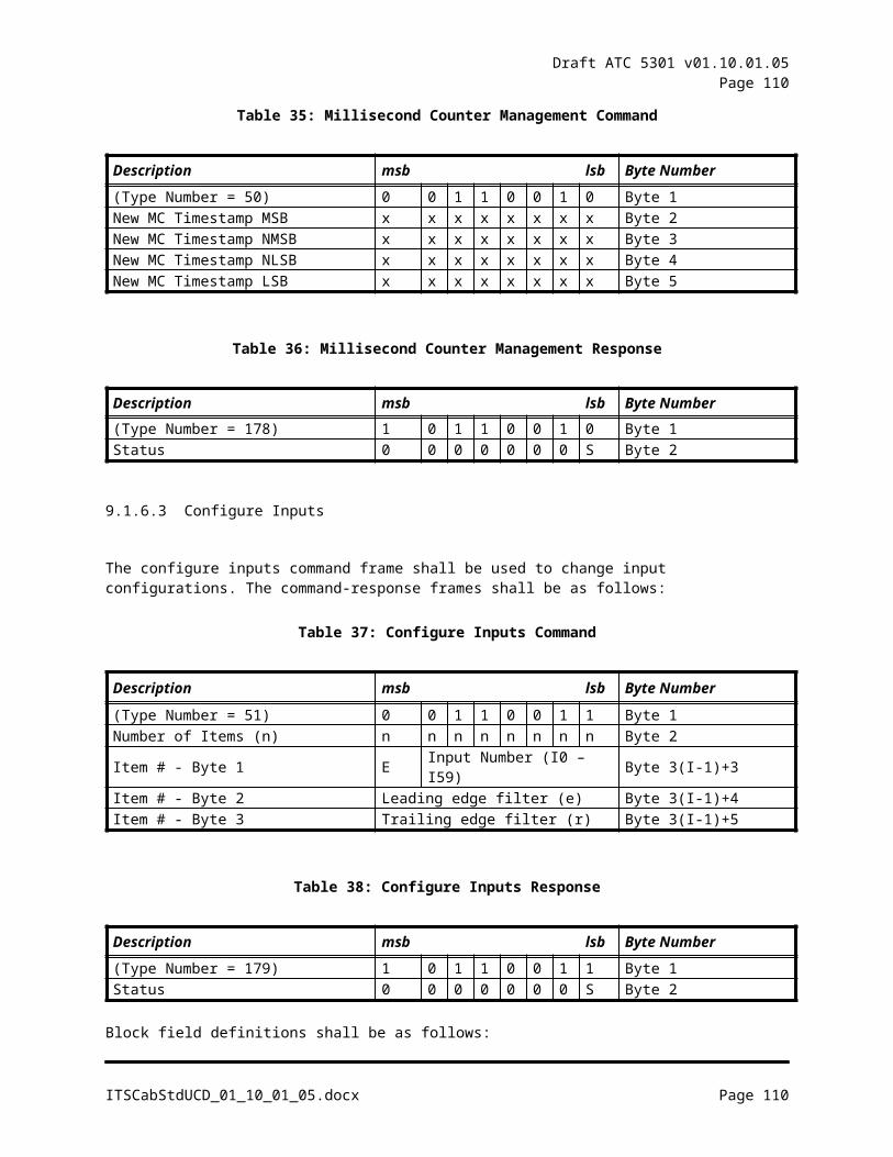
Draft ATC 5301 v01.10.01.05Page 110
9.3.6 Message Timing
The 2202 HDSP/FU and ADU shall begin its response to command frames from the CMU-2212 within a designated period of time following the correct reception of a complete command frame including the closing flag. This period shall be known as the Service Time and shall have a maximum value of 50 microseconds. The 2202 HDSP/FU and ADU TXD link output shall be in the high impedance state outside of the interval defined by the Service Time plus Response Time.
The 2202 HDSP/FU and ADU shall complete its transmission of the response frame including the closing flag within a designated time known as the Response Time, depending on the number of bytes transmitted in the response frame. The 2202 HDSP/FU and ADU TXD link output shall transition to a high impedance state a maximum of 25 microseconds following the transmission of the closing flag. The Response Time period shall have a maximum value of:
(1.1)*(# of bytes in information field + 6)*(10/307200)
Note that due to the transparency mechanism, any occurrence of the flag byte (0x7E) or control escape byte (0x7D) in the information field adds a second byte to the count. Thus, the number of bytes in the information field could be higher if data characters are 0x7E or 0x7D.
Following the transmission of each command frame, there shall be a Dead Time during which the CMU-2212 does not transmit. This Dead Time shall be a minimum of the Service Time plus the Response Time.
9.3.7 SB #3 Information Field Formats
The first eight bits in each information field shall contain the frame Type Number. There shall be a maximum of 64 different command frame types defined by this standard and 64 different response frame types defined by this standard. Additionally, there shall be 64 different command frame types reserved for manufacturers use and 64 different response frame types reserved for manufacturer’s use, as outlined below.
Table 61: SB #3 Frame Types
Frame Types Funcition0-63 Command Frame
64-127 Command Frame, Manufacturers Use128-191 Response Frame192-255 Response Frame, Manufacturers Use
The information fields of frame types 64 through 127 and 192 through 255 shall contain a manufacturer specific code (MFG Code). The manufacturer specific code is a 16 bit binary number which shall be placed in bits 9–24 of the information field. These codes are maintained and issued by NEMA.Reserved bits shall always be set to zero by the transmitting station.
The SB #3 frames to and from the model 2220 shall use only Command frame types 64-127 and corresponding Response frame types 192-255.
The intention in placing manufacturer specific codes in frame types that are reserved for manufacturers use is to allow equipment to differentiate between frames that may contain the same frame type. (Authorized Engineering Information.)
ITSCabStdUCD_01_10_01_05.docx Page 110
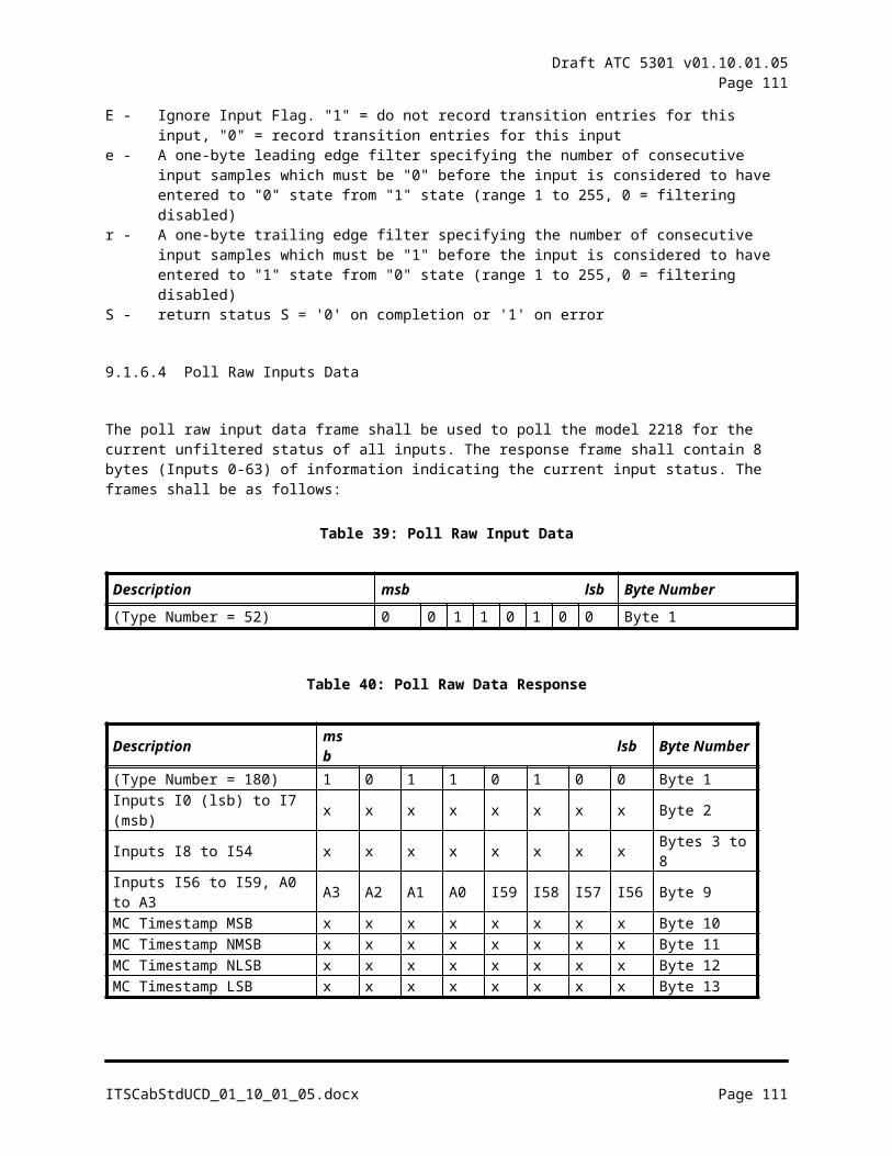
Draft ATC 5301 v01.10.01.05Page 111
9.3.8 2202 HDSP/FU SB3 Frame Types
9.3.8.1Voltage / Current Encoding
RMS voltage and current data shall be reported as a 14 bit positive integer, and shall be encoded in the frames as follows:
The LSB byte in the frame is composed of the least significant 7 bits (b6:b0) of the reported value with bit 7 of the frame byte set to “1”.
The MSB byte in the frame is composed of the next most significant 7 bits (b13:b7) of the reported value with bit 7 of the frame byte set to “1”.
Bit # 7 6 5 4 3 2 1 0
LSB 1 b6 b5 b4 b3 b2 b1 b0
MSB 1 b13 b12 b11 b10 b9 b8 b7
9.3.8.22202 HDSP/FU Status
9.3.8.2.1Type 01 Command – HDSP Status
Table 62: SB #3 Type 01 Command
Byte # Contents Description1 01 Frame Type2 Channel Fault Indicator Channel ID Indicators
b0 = Channel 1a indicator activeb1 = Channel 2a indicator activeb2 = Channel 1b indicator activeb3 = Channel 2b indicator activeb4 = Display Sleep modeb5:6 = reservedb7 = 1
3 Channel Output Disable Channel 1, 2 Output Disableb0 = Channel 1 Red Disableb1 = Channel 1 Yellow Disableb2 = Channel 1 Green Disableb3 = Channel 2 Red Disableb4 = Channel 2 Yellow Disableb5 = Channel 2 Green Disableb6 = Reservedb7 = 1
9.3.8.2.2Type 129 Response – HDSP Status
Table 63: SB #3 Type 129 Response
Byte # Contents Description1 129 Frame Type2 Status HDSP Status
ITSCabStdUCD_01_10_01_05.docx Page 111
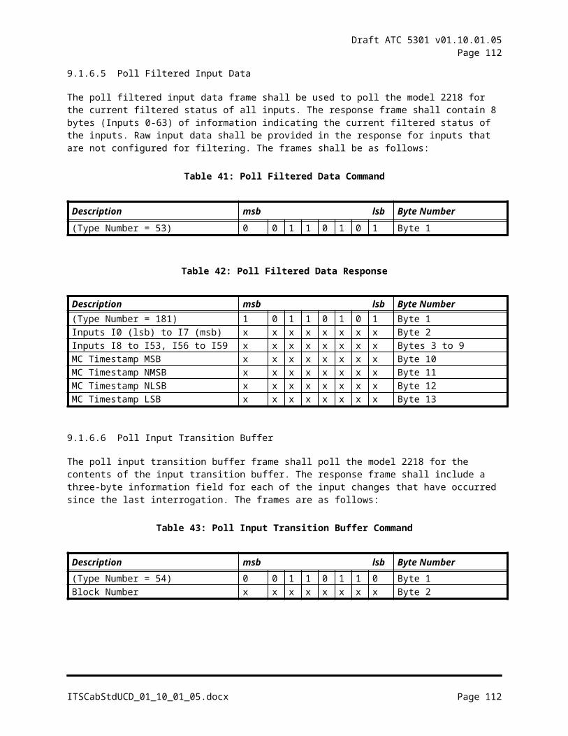
Draft ATC 5301 v01.10.01.05Page 112
Byte # Contents Descriptionb0 = set to 1 if +24 VDC MONITOR input is Lowb1 = set if 2202 HDSP/FU has reset since last pollb2 = set if last RMS period data was not transmittedb3 = diagnostic failureb4:6 = Reservedb7 = 1
3 Signal Power LSB HV+SIGNAL or LV+SIGNAL RMS Voltage (Units are 0.1 Vrms)4 Signal Power MSB5 Channel 1 Red LSB Field Output RMS Voltage (Units are 0.1 Vrms)6 Channel 1 Red MSB7 Channel 1 Yellow LSB8 Channel 1 Yellow MSB9 Channel 1 Green LSB
10 Channel 1 Green MSB11 Channel 2 Red LSB12 Channel 2 Red MSB13 Channel 2 Yellow LSB14 Channel 2 Yellow MSB15 Channel 2 Green LSB16 Channel 2 Green MSB17 Channel 1 Red LSB Field Output RMS Current (Units are 1 Milliampere)18 Channel 1 Red MSB19 Channel 1 Yellow LSB20 Channel 1 Yellow MSB21 Channel 1 Green LSB22 Channel 1 Green MSB23 Channel 2 Red LSB24 Channel 2 Red MSB25 Channel 2 Yellow LSB26 Channel 2 Yellow MSB27 Channel 2 Green LSB28 Channel 2 Green MSB29 Channel Input Control Channel 1, 2 Input State (1=Input Active)
b0 = Channel 1 Red Onb1 = Channel 1 Yellow Onb2 = Channel 1 Green Onb3 = Channel 2 Red Onb4 = Channel 2 Yellow Onb5 = Channel 2 Green Onb6 = reservedb7 = 1
30 Channel Output Disabled
Channel 1, 2 (1=Output Disabled)b0 = Channel 1 Red Disabledb1 = Channel 1 Yellow Disabledb2 = Channel 1 Green Disabledb3 = Channel 2 Red Disabledb4 = Channel 2 Yellow Disabledb5 = Channel 2 Green Disabledb6 = reservedb7 = 1
ITSCabStdUCD_01_10_01_05.docx Page 112
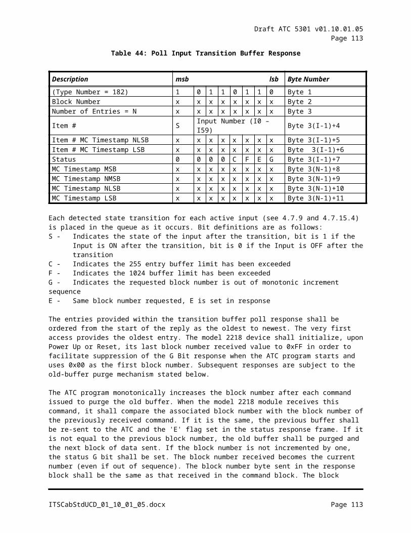
Draft ATC 5301 v01.10.01.05Page 113
9.3.8.2.3Type 02 Command – HDFU Status
Table 64: SB #3 Type 02 Command
Byte # Contents Description1 02 Frame Type2 Channel Output Disable Channel 1, 2 Output Disable (1=Output Disabled)
b0 = Channel 1-1 Disableb1 = Channel 1-2 Disableb2 = Channel X Disable (Ch1 Green)b3 = Channel Y Disable (Ch 2 Red)b4 = Channel 2-1 Disableb5 = Channel 2-2 Disableb6 = Reservedb7 = 1
3 Channel Fault Indicator Channel ID Indicatorsb0 = Channel 1a indicator activeb1 = Channel 2a indicator activeb2 = Channel 1b indicator activeb3 = Channel 2b indicator activeb4 = Display Sleep modeb5 = Use display bits b0:3b6 = reservedb7 = 1If b5 is set, then the HDFU will use b3:b0 to drive the Channel ID LEDs.
9.3.8.2.4Type 130 Response – HDFU Status
Table 65: SB #3 Type 130 Response
Byte # Contents Description1 130 Frame Type2 HDFU Status HDFU Status
b0 = Reservedb1 = set if HDFU has reset since last pollb2 = set if last RMS period data was not transmittedb3 = diagnostic failureb4:6 = Reservedb7 = 1
3 Signal Power LSB HV+SIGNAL or LV+SIGNAL RMS Voltage (Units are 0.1 Vrms)4 Signal Power MSB5 Channel 1-1 LSB Field Output RMS Voltage (Units are 0.1 Vrms)6 Channel 1-1 MSB7 Channel 1-2 LSB8 Channel 1-2 MSB9 Channel X LSB
10 Channel X MSB11 Channel Y LSB12 Channel Y MSB
ITSCabStdUCD_01_10_01_05.docx Page 113
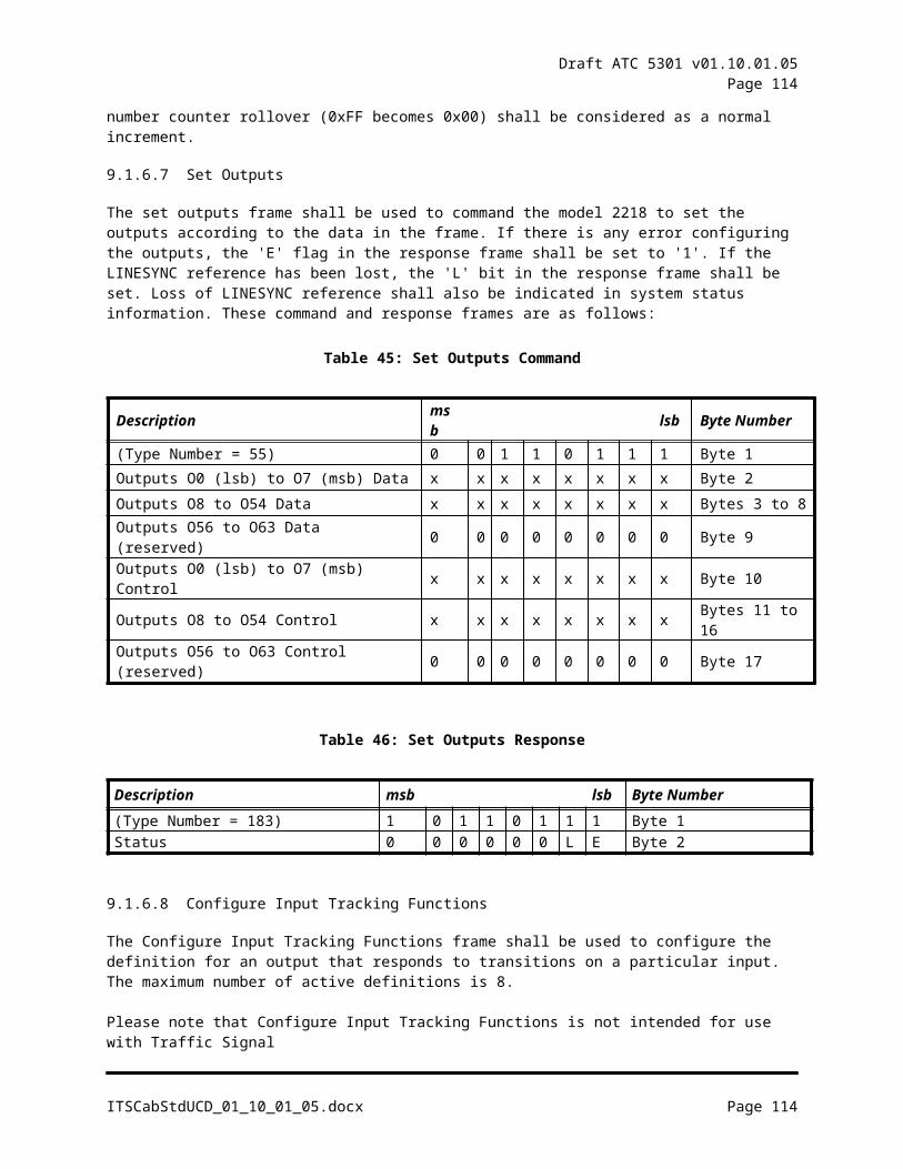
Draft ATC 5301 v01.10.01.05Page 114
Byte # Contents Description13 Channel 2-1 LSB14 Channel 2-1 MSB15 Channel 2-2 LSB16 Channel 2-2 MSB17 Channel 1-1 LSB Field Output RMS Current (Units are 1 Milliampere)18 Channel 1-1 MSB19 Channel 1-2 LSB20 Channel 1-2 MSB21 Channel X LSB22 Channel X MSB23 Channel Y LSB24 Channel Y MSB25 Channel 2-1 LSB26 Channel 2-1 MSB27 Channel 2-2 LSB28 Channel 2-2 MSB29 Channel Input Control Channel 1, 2 Input State
b0 = 1-1 Control Onb1 = 1-2 Control Onb2 = Channel X Onb3 = Channel Y Onb4 = 2-1 Control Onb5 = 2-2 Control Onb6 = Reservedb7 = 1
30 Channel Output Disabled
Channel 1, 2 (1=Output Disabled)b0 = Channel 1-1 Disabledb1 = Channel 1-2 Disabledb2 = Channel X Disabledb3 = Channel Y Disabledb4 = Channel 2-1 Disabledb5 = Channel 2-2 Disabledb6 = Reservedb7 = 1
9.3.8.2.5Type 60 Command – HDFU Module ID
Table 66: SB #3 Type 60 Command
Byte # Contents Description1 60 Frame Type
9.3.8.2.6Type 188 Response – HDFU Module ID
Table 67: SB #3 Type 188 Response
ITSCabStdUCD_01_10_01_05.docx Page 114
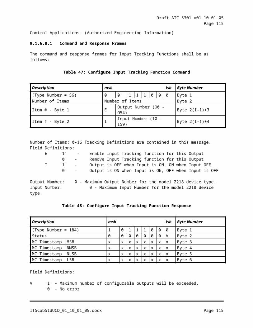
Draft ATC 5301 v01.10.01.05Page 115
Byte # Contents Description1 188 Frame Type2 Device Type 2202 HDSP/FU Type
1 = 2202 HDSP/FU-HV2 = 2202 HDSP/FU-LV3 = 2202 HDSP/FU-VHV (reserved)4 = 2200 HDSP-HV5 = 2200 HDSP-LV6 = 2200 HDSP-VHV (reserved)7 = 2204 HDFU-HV8 = 2204 HDFU-LV9 = 2204 HDFU-VHV (reserved)10:255 = Reserved
3:62 ID String Manufacturer-specified Identification StringA packed 60 character ID shall be stored in ASCII format. Allowable characters are 020h through 07Eh. If less than 60 characters are used, the unused locations shall be set to 20h. Default programming shall be 20h.
9.3.8.2.7Type 128 Response – Negative Acknowledge
This frame shall be transmitted from the 2202 HDSP/FU to the CMU as a negative acknowledge response frame if the 2202 HDSP/FU correctly receives a Type 01 command frame or a Type 02 command frame with an invalid parameter, including the Frame Type.
Table 68: SB #3 Type 128 Response
Byte # Contents Description1 128 Frame Type2 Status 2202 HDSP/FU SB #3 Error Type
b0 = set to 1 if invalid frame type receivedb1 = set to 1 if invalid parameter is receivedb2:6 = reservedb7 = 1
3 Parameter Number Invalid Parameter Byte NumberThe byte number of the Type 01 or Type 02 frame that contained the invalid parameter. If more than one parameter is invalid then this offset shall be the first byte in the frame in error.
9.3.9 Model 2220 SB3 Frame Types
The model 2220 shall respond to serial data frames transmitted by the CMU2212 on the Serial Bus #3.
9.3.9.1Type 70 Command – Set LEDs
Table 69: ADU Type 70 Command
Byte # Contents Description1 0x46 Frame Type
ITSCabStdUCD_01_10_01_05.docx Page 115
Draft ATC 5301 v01.10.01.05Page 116
Byte # Contents Description2 0x00-0xFF MFG Code LS3 0x00-0xFF MFG Code MS4 0x00-0x01 LED Control
b0 = LED Enableb7:1 = reserved
5 Ch 8:1
Blue LEDs6 Ch 16:97 Ch 24:178 Ch 32:259 Ch 8:1
Red LEDs10 Ch 16:911 Ch 24:1712 Ch 32:2513 Ch 8:1
Yellow LEDs14 Ch 16:915 Ch 24:1716 Ch 32:2517 Ch 8:1
Green LEDs18 Ch 16:919 Ch 24:1720 Ch 32:25
9.3.9.2Type 70 Response – Set LEDs
Table 70: ADU Type 70 Response
Byte # Contents Description1 0xC6 Frame Type2 0x00-0xFF MFG Code LS3 0x00-0xFF MFG Code MS4 0x00-0x01 Button Status (A value of 1 shall be set when the button is in the
pressed state)b0 = Helpb1 = Nextb2 = Nextb3 = Backb4 = Selectb5 = Exitb7:6 = reserved
9.3.9.3Type 70 Command – Set LCD
Table 71: ADU Type 71 Command
Byte # Contents Description1 0x47 Frame Type
ITSCabStdUCD_01_10_01_05.docx Page 116
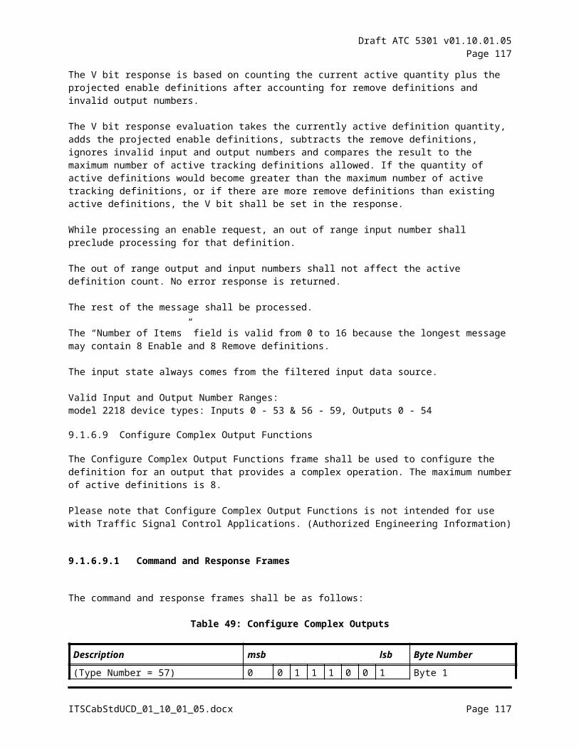
Draft ATC 5301 v01.10.01.05Page 117
Byte # Contents Description2 0x00-0xFF MFG Code LS3 0x00-0xFF MFG Code MS4 0x00-0x03 LCD Control
b0 = Back Light Enableb1 = Heater Enableb7:2 = reserved
5 0x01-0x04 LCD Line Number6 Ascii Char ASCII Text for the 20 Character Line
Character #1 is the leftmost character7 Ascii Char8 Ascii Char9 Ascii Char
10 Ascii Char11 Ascii Char12 Ascii Char13 Ascii Char14 Ascii Char15 Ascii Char16 Ascii Char17 Ascii Char18 Ascii Char19 Ascii Char20 Ascii Char21 Ascii Char22 Ascii Char23 Ascii Char24 Ascii Char25 Ascii Char
9.3.9.4Type 70 Response – Set LCD
Table 72: ADU Type 71 Response
Byte # Contents Description1 0xC7 Frame Type2 0x00-0xFF MFG Code LS3 0x00-0xFF MFG Code MS4 0x00-0x01 Button Status (A value of 1 shall be set when the button is in the
pressed state)b0 = Helpb1 = Nextb2 = Nextb3 = Backb4 = Selectb5 = Exitb7:6 = reserved
ITSCabStdUCD_01_10_01_05.docx Page 117

Draft ATC 5301 v01.10.01.05Page 118
10 PRODUCT SAFETY
10.1 Mercury
Mercury shall not be used in components that will create a disposal issue.
10.2 Shock Hazard
For the ATCC Low Voltage Version, voltages shall be constrained to eliminate shock hazard as defined in NFPC 70 B E.
10.3 Arc Flash
Electromotive force of electrical signals shall be constrained to eliminate arc flash hazard as defined in NFPC 70 B E
10.4 Safe Operation During Service and Replacement
The cabinet shall be capable of remaining in Flashing Mode when any element of the cabinet is removed or replaced except the Power Service Functionality and Field Termination functionality.
11 ENVIRONMENTAL AND TESTING REQUIREMENTS
NOTE: All references in this section to NEMA TS2 explicitly refer to the NEMA Standards Publication TS2-2016 v3.07, Traffic Controller Assemblies with NTCIP Requirements. 11.1 General
This section establishes the environmental and operational conditions for a First Article ATCC cabinet, and defines the minimum test procedures which may be used to demonstrate conformance of an ATCC cabinet with the provisions of the Standard.
Testing shall be performed either within an environmental chamber or on a bench.
These test procedures do not verify equipment performance under every possible combination of environmental requirements covered by the Standard. However, nothing in this testing profile shall be construed as to relieve the requirement that the equipment provided must fully conform with the Standard under all environmental conditions stated herein.
11.2 Inspection
A visual and physical inspection of the ATCC unit shall verify mechanical, dimensional and assembly conformance to all parts of this standard.
11.3 Testing Certification
A complete quality control and final test report shall be supplied with each item.
11.4 Definitions of Design Acceptance Testing (DAT) and Production Testing.
Design Acceptance Testing (DAT) is performed on the first article ATCC unit and is a part of the pre-production process.
ITSCabStdUCD_01_10_01_05.docx Page 118
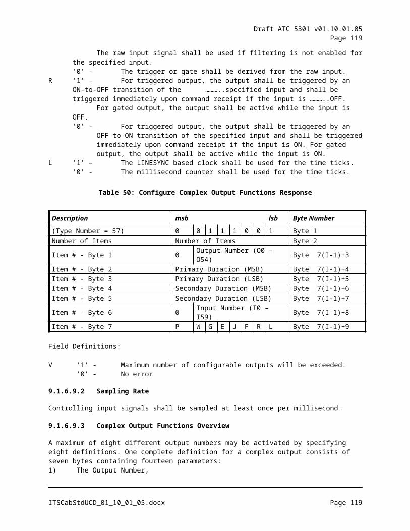
Draft ATC 5301 v01.10.01.05Page 119
Production testing is performed on all units prior to their shipment to an agency.
11.5 Environmental and Operating Requirements
The requirements (voltage, temperature, etc.) of this section shall apply in any combination.
11.5.1 Voltage and Frequency
11.5.1.1.1 Operating Voltage
The nominal operating voltage shall be 120 VAC, unless otherwise noted for the ATCC High Voltage version (HV) and at 48 VDC for the ATCC Low Voltage version (LV).
11.5.1.1.2 Operating Frequency
The nominal AC line operating frequency range shall be 60 Hz (±3.0 Hz), unless otherwise noted for the ATCC High Voltage version (HV) and at DC for the ATCC Low Voltage version (LV).
11.5.2 Transients, Power Service (DAT)
The ATC unit under test shall meet all requirements as defined in NEMA TS2, Section 2.1.6, Transients, Power Service.
11.5.3 Nondestructive Transient Immunity (DAT)
The ATC unit under test shall meet all requirements as defined in NEMA TS2, Section 2.1.8, Nondestruct Transient Immunity, with the following variations:
Test voltage amplitude shall be 2000 ± 100 V, both positive and negative polarity.
11.5.4 Temperature and Humidity
The ATC unit under test shall maintain all programmed functions when the temperature and humidity ambients are within the specified limits defined herein.
11.5.4.1.1 Ambient Temperature
The operating ambient temperature range shall be from -37˚C to +74˚C. The storage temperature range shall be from -45˚C to +85˚C.
The rate of change in ambient temperature shall not exceed 18˚C per hour, during which the relative humidity shall not exceed 95 percent.
11.5.4.1.2 Humidity
The relative humidity shall not exceed 95 percent non-condensing over the temperature range of -37˚C to +74˚C.
Above +46˚C, constant absolute humidity shall be maintained. This will result in the relative humidities shown in Table 73 for dynamic testing.
ITSCabStdUCD_01_10_01_05.docx Page 119
Draft ATC 5301 v01.10.01.05Page 120
Table 73: Ambient Temperature versus Relative Humidity At Barometric Pressures(29.92 In. Hg.) (Non-Condensing)
Ambient Temperature/Dry Bulb (˚C)
Relative Humidity(in%)
Ambient Temperature/Wet Bulb (˚C)
-37.0 to 1.1 10 -17.2 to 42.71.1 to 46.0 95 42.7
48.8 70 42.754.4 50 42.760.0 38 42.765.4 28 42.771.2 21 42.774.0 18 42.7
11.6 Test Facilities
All instrumentation required in the test procedures, such as voltmeters, ammeters, thermocouples, pulse timers, etc. shall be selected in accordance with good engineering practice. Calibration records for all test equipment shall be provided with test documentation. In all cases where time limit tests are required, the allowance for any instrumentation errors shall be included in the limit test.
1. Variable Voltage Source: A variable source capable of supplying 20 A from 0 VAC to 135 VAC for the ATCC High Voltage version and 0- 48 VDC for the ATCC Low Voltage version.
2. Environmental Chamber: An environmental chamber capable of attaining temperatures of -37˚C to +74˚C and relative humidities given in Table 73.
3. Transient Generator(s): Transient generator(s) capable of supplying the transients outlined in 11.5.2 and 11.5.3.
11.7 Test Procedures: Transients, Temperature, Voltage and Humidity
11.7.1 Test A: Placement in Environmental Chamber and Check-Out of Hook-Up (DAT and Production Testing)
The ATC unit under test shall meet all requirements as defined in NEMA TS2, Section 2.2.7.1, Test A: Placement in Environmental Chamber and Check-Out of Hook-Up, with the following variations:
For DAT purposes only, the transient generator shall be connected to the AC input circuit at a point at least 25 feet from the AC power source and not over 10 feet from the input to the test unit
Upon the satisfactory completion and verification of the test hook-up, proceed with Test B (DAT) or Test C (DAT and Production Testing). Error: Reference source not found describes the test profile used for Tests C through G to demonstrate the ability of the test unit to function reliably under stated conditions of temperature, voltage and humidity. Where the characteristics of Error: Reference source not found differ from those specified in NEMA TS2, Figure 2-1, those in Error: Reference source not found will apply unless specified otherwise.
11.7.2 Test B: Temperature Cycling and Applied Transient Tests (Power Service) (DAT)
Note: In this section the term “dwell” refers to an application in its resting state awaiting inputs, and the actual resting state depends on the application. The goal is to determine if the transients introduced affect
ITSCabStdUCD_01_10_01_05.docx Page 120
Draft ATC 5301 v01.10.01.05Page 121
the operation of the application by triggering false inputs and/or outputs causing inappropriate application program activity (e.g. improper timing, false calls, error alarms, etc).
The ATC unit under test shall meet all requirements as defined in NEMA TS2, Section 2.2.7.2, Test B: Transient Tests (Power Service), with the following variations:
Test voltage amplitude in Step 13 shall be 2000 ± 100 V, both positive and negative polarity.
Figure 23: Test Profile
NOTES:1. The rate of change in temperature shall not exceed 18˚ C per hour.2. Humidity controls shall be set in conformance with the humidities given in Table 8-1
during the temperature change between Test D and Test E.3. If a change in both voltage and temperature are required for the next test, the voltage
shall be selected prior to the temperature change.
11.7.3 Test C: Low-Temperature Low-Voltage Tests (DAT and Production Testing)
The ATC unit under test shall meet all requirements as defined in NEMA TS2, Section 2.2.7.3, Test C: Low-Temperature Low-Voltage Tests, with the following variations:
Utilize Error: Reference source not found for the test profile (temperature: -37˚C, low voltage). Skip tests 2.c.2) 2.2.11 Timing Accuracy Tests and 2.c.3) 2.2.11.2 Repeatability.
11.7.4 Test D: Low-Temperature High-Voltage Tests (DAT and Production Testing)
The ATC unit under test shall meet all requirements as defined in NEMA TS2, Section 2.2.7.4, Test D: Low-Temperature High-Voltage Tests, with the following variations:
ITSCabStdUCD_01_10_01_05.docx Page 121
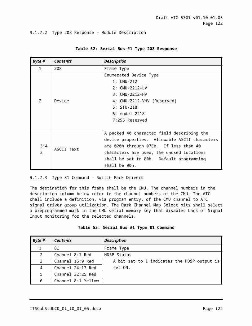
Draft ATC 5301 v01.10.01.05Page 122
Utilize Error: Reference source not found for the test profile (temperature: -37˚C). Skip tests 2.c.2) 2.2.11 Timing Accuracy Tests and 2.c.3) 2.2.11.2 Repeatability.
11.7.5 Test E: High-Temperature High-Voltage Tests (DAT and Production Testing)
The ATC unit under test shall meet all requirements as defined in NEMA TS2, Section 2.2.7.5, Test E: High-Temperature High-Voltage Tests, with the following variations:
Utilize Table Table 73for the humidity controls. In Step 3, utilize the temperature range of +1.1˚ C to +46˚ C and +42.7˚ C wet bulb. Skip tests 2. 2.2.11 Timing Accuracy Tests and 2. 2.2.11.2 Repeatability.
11.7.6 Test F: High-Temperature Low-Voltage Tests (DAT and Production Testing)
The ATC unit under test shall meet all requirements as defined in NEMA TS2, Section 2.2.7.6, Test F: High-Temperature Low-Voltage Tests, with the following variations:
Utilize Error: Reference source not found for the test profile (low voltage). In Step 2, utilize +42.7˚ C wet bulb. Skip tests 2. 2.2.11 Timing Accuracy Tests and 2. 2.2.11.2 Repeatability.
11.7.7 Test G: Test Termination (All tests)
The ATC unit under test shall meet all requirements as defined in NEMA TS2, Section 2.2.7.7, Test G: Test Termination, with the following variations:
Utilize Error: Reference source not found for the test profile.
11.7.8 Test H: Appraisal of Equipment Under Test
The ATC unit under test shall meet all requirements as defined in NEMA TS2, Section 2.2.7.8, Test H: Appraisal of Equipment Under Test.
11.8 Vibration Test (DAT)
The ATC unit under test shall meet all requirements as defined in NEMA TS2, Section 2.2.8, Vibration Test.
Shock and vibration tests shall be performed prior to environmental tests.
11.9 Shock (Impact) Test (DAT)
11.9.1 Purpose of Test
The ATC unit under test shall meet all requirements as defined in NEMA TS2, Section 2.2.9, Shock (Impact) Test, with the following modifications:
a) Program the table to subject the test unit to a 10G force having a duration of 11 ms.b) The test shall use a waveform suitable to simulate a drop test, such as saw tooth. The
waveform shall be a saw tooth with 11 ms rise time and 0 ms fall time.c) Subject the test unit to the above test setup three times in both the positive and negative
direction.
Shock and vibration tests shall be performed prior to environmental tests.
ITSCabStdUCD_01_10_01_05.docx Page 122
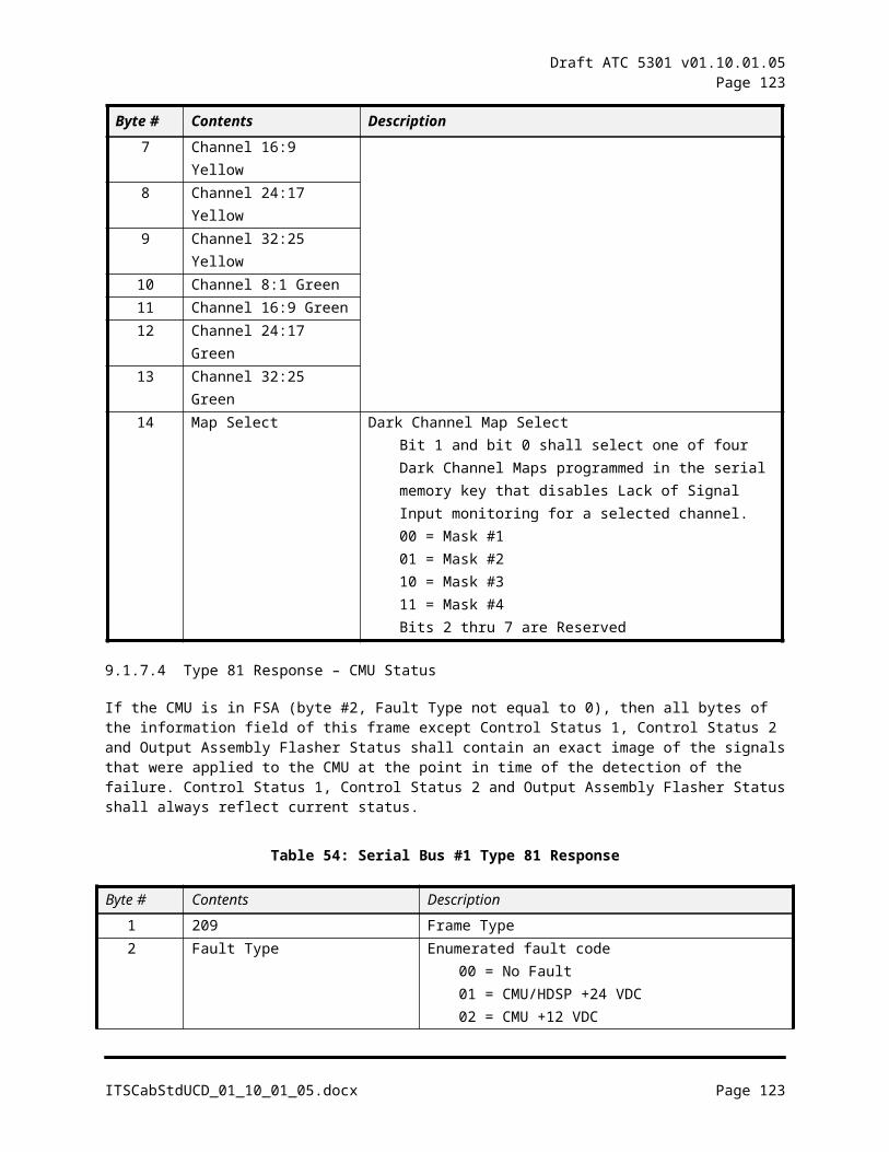
Draft ATC 5301 v01.10.01.05Page 123
12 ACRONYMS
Term DefinitionAASHTO American Association of State Highway and Transportation OfficialsAC alternating currentATC Advanced Transportation ControllerATCC ATC CabinetCB Circuit BreakerCBD Central Business DistrictConOps Concept of OperationsDC direct currentEMI electromagnetic interferenceFHWA Federal Highway AdministrationESD Electrostatic DischargeGFI Ground Fault InterruptIEEE Institute of Electrical and Electronics EngineersI/F interfaceI/O input/outputIEC International Electrotechnical CommissionIMSA International Municipal Signal AssociationIPC Formerly, the Institute for Printed Circuits. This same institution was
later called the Institute Interconnecting and Packaging Electronic Circuits. It is now referred to as IPC-Association Connecting Electronics Industries.
ITE Institute of Transportation EngineersITS Intelligent Transportation SystemJPO Joint Program OfficeLED light emitting diodeMTBF mean time between failuresNEC National Electrical CodeNEMA National Electrical Manufacturers AssociationNRTL Nationally Recognized Testing LabNTCIP National Transportation Communications for ITS ProtocolNFPA National Fire Protection AssociationPF power factorRFI radio frequency interferenceSDO Standard Development OrganizationSEMP System Engineering Management PlanSEP Systems Engineering ProcessSSC Small-Sized CabinetStdRS Standards Requirements SpecificationStdHLD Standards High Level DesignTFCS transportation field cabinet systemUPS Uninterruptible Power SourceUSA United States of America USDOT United States Department of TransportationVAC voltage alternating currentVDC voltage direct currentWG Working Group
ITSCabStdUCD_01_10_01_05.docx Page 123