pv energy payback - sunlight solar...
TRANSCRIPT
Photovoltaic technology is a fantastic miracle of science that silently converts sunlight into streaming electrons that can be used to do work. While sunlight magically falls from the sky, PV modules and their associated components do not—each consumes energy and resources along every step of the production process, from material harvesting to manufacturing to assembly and shipping.
A common myth about PV technology is that it takes more energy to produce a PV system than the system will produce in its lifetime. Thankfully, this is not the case. Recent studies of energy payback time (EPBT) estimate that it takes a PV system one to three years to produce the same amount of energy that it took to manufacture it. Given that a PV system will continue to produce electricity for 30 years or more, a PV system’s lifetime production will far exceed the energy it took to produce it. Here’s an in-depth look at the embodied energy along the way.
Module Manufacturing MethodsA batteryless grid-tied PV system has many parts—modules and mounts, inverter(s), and wiring components (including conduit, fittings, electrical boxes, wire, and overcurrent protection). Each part of a PV system takes energy to both produce and transport (embodied energy), but of all of them, the modules require the most energy to manufacture—about 93% of the entire system.
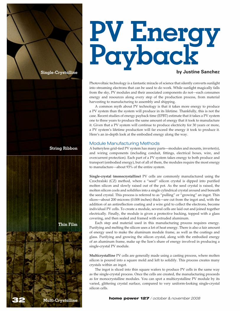
Single-crystal (monocrystalline) PV cells are commonly manufactured using the Czochralski (CZ) method, where a “seed” silicon crystal is dipped into purified molten silicon and slowly raised out of the pot. As the seed crystal is raised, the molten silicon cools and solidifies into a single cylindrical crystal around and beneath the seed crystal. This process is referred to as “pulling” or “growing” an ingot. Thin slices—about 200 microns (0.008 inches) thick—are cut from the ingot and, with the addition of an antireflection coating and a wire grid to collect the electrons, become individual PV cells. To create a module, several cells are laid out and joined together electrically. Finally, the module is given a protective backing, topped with a glass covering, and then sealed and framed with extruded aluminum.
Each step and material used in this manufacturing process requires energy. Purifying and melting the silicon uses a lot of heat energy. There is also a fair amount of energy used to make the aluminum module frame, as well as the coatings and glass. Purifying and growing the silicon crystal, along with the embodied energy of an aluminum frame, make up the lion’s share of energy involved in producing a single-crystal PV module.
Multicrystalline PV cells are generally made using a casting process, where molten silicon is poured into a square mold and left to solidify. This process creates many crystals within an ingot.
The ingot is sliced into thin square wafers to produce PV cells in the same way as the single-crystal process. Once the cells are created, the manufacturing proceeds as for monocrystalline modules. You can spot a multicrystalline PV module by its varied, glittering crystal surface, compared to very uniform-looking single-crystal silicon cells.
home power 127 / october & november 200832
PV Energy Payback
by Justine SanchezSingle-Crystalline
String Ribbon
Thin Film
Multi-Crystalline
Multicrystalline PV modules do require less energy to produce than CZ-produced monocrystalline PV modules partly because the cooling process for the cast ingot uses less energy. The energy payback times for multicrystalline PV systems are about 15% less than for monocrystalline PV systems.
String Ribbon Silicon. Another way to produce a crystalline PV module is to grow thin ribbons of silicon that can be cut into individual cells. One method that produces these types of cells pulls two parallel wires out of a vat of molten silicon. As the wires are pulled up, a thin sheet of silicon the width of a finished cell stretches and hardens between them, much like soapy film stretches between the sides of a child’s bubble wand. Because the ribbon silicon sheet is so thin, it does not need to be sliced as ingots do, but is sectioned into cell-sized lengths to make individual PV cells. The ribbon silicon cells are formed into modules the same way as the monocrystalline and multicrystalline PV technologies.
The ribbon technique reduces the energy and silicon crystal waste associated with sawing the wafers (kerf loss) from a crystalline ingot, reducing the energy payback time compared to monocrystalline by about 25% and multicrystalline PV by approximately 12%.
Thin-film PV modules use a deposition process, in which different layers of the PV cell are sprayed directly onto a
substrate. Since there are no individual crystals to break, this substrate can be flexible and virtually any shape or size. The PV cells are completed after all the layers of the semiconductor material have been applied to the substrate by scribing the entire module into individual cells with lasers. Thin-film modules use a transparent conducting oxide (also applied as a layer in the deposition process) for electrical contacts, instead of an unbendable metal grid as crystalline cells.
www.homepower.com
energy payback
33
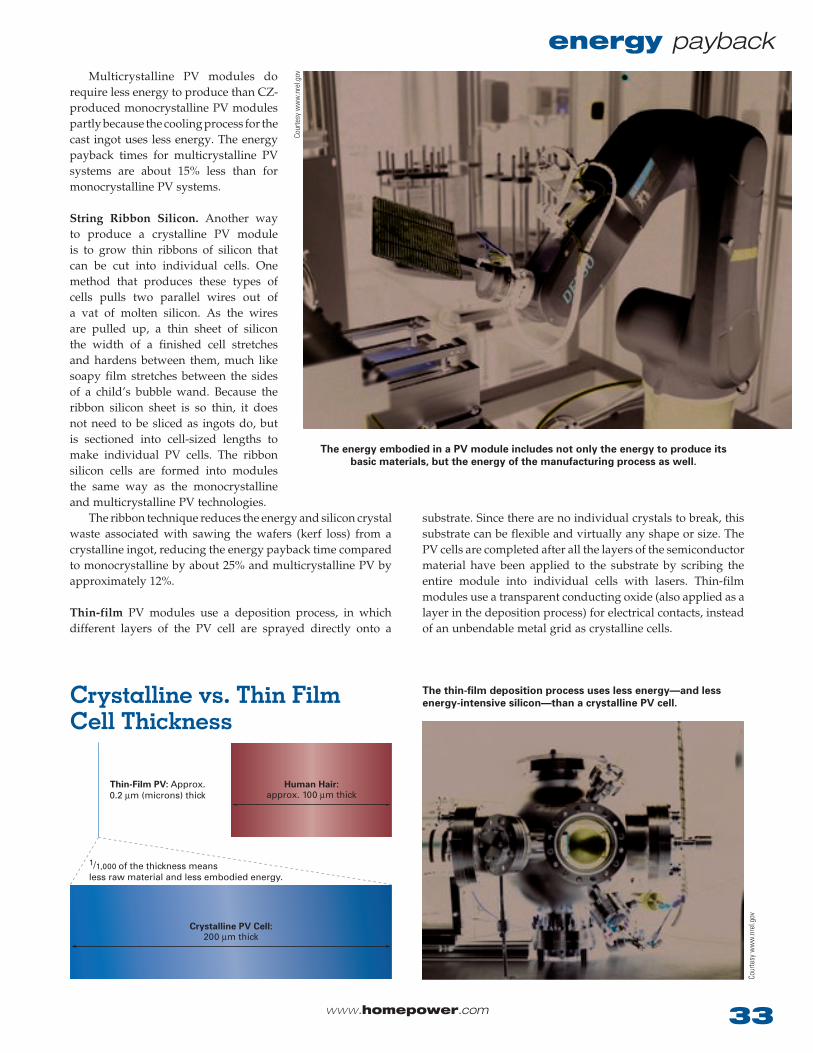
The energy embodied in a PV module includes not only the energy to produce its basic materials, but the energy of the manufacturing process as well.
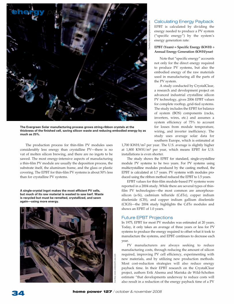
The thin-film deposition process uses less energy—and less energy-intensive silicon—than a crystalline PV cell.
Thin-Film PV: Approx. 0.2 m (microns) thick
Crystalline PV Cell: 200 m thick
Human Hair:approx. 100 m thick
1/1,000 of the thickness means less raw material and less embodied energy.
Crystalline vs. Thin Film Cell ThicknessCo
urte
sy w
ww
.nre
l.gov
Cour
tesy
ww
w.n
rel.g
ov
The production process for thin-film PV modules uses considerably less energy than crystalline PV—there is no vat of molten silicon brewing, and there are no ingots to be sawed. The most energy-intensive aspects of manufacturing a thin-film PV module are usually the deposition process, the substrate itself, the aluminum frame, and the glass or plastic covering. The EPBT for thin-film PV systems is about 50% less than for crystalline PV systems.
home power 127 / october & november 200834
Calculating Energy PaybackEPBT is calculated by dividing the energy needed to produce a PV system (“specific energy”) by the system’s energy generation rate:
EPBT (Years) = Specific Energy (KWH) ÷ Annual Energy Generation (KWH/year)
Note that “specific energy” accounts not only for the direct energy required to produce PV systems, but also the embodied energy of the raw materials used in manufacturing all the parts of the PV system.
A study conducted by CrystalClear, a research and development project on advanced industrial crystalline silicon PV technology, gives 2006 EPBT values for complete rooftop, grid-tied systems. The study includes the EPBT for balance of system (BOS) components (racks, inverters, wires, etc.) and assumes a system efficiency of 75% to account for losses from module temperature, wiring, and inverter inefficiency. The study uses average solar data for southern Europe, which is estimated at
1,700 KWH/m2 per year. The U.S. average is slightly higher at 1,800 KWH/m2 per year, which means EPBT for U.S. installations is even shorter.
The study shows the EPBT for standard, single-crystalline module PV systems to be two years. For PV systems using multicrystalline modules produced by the casting method, the EPBT is calculated at 1.7 years. PV systems with modules pro-duced using the ribbon method reduced the EPBT to 1.5 years.
EPBT values for thin-film module-based PV systems were reported in a 2004 study. While there are several types of thin-film PV technologies—the most common are amorphous-silicon (a-Si), cadmium telluride (CdTe), copper indium diselenide (CIS), and copper indium gallium diselenide (CIGS)—the 2004 study highlights the CdTe modules and shows an EPBT of 1.0 years.
Future EPBT ProjectionsIn 1975, EPBT for most PV modules was estimated at 20 years. Today, it only takes an average of three years or less for PV systems to produce the energy required to offset what it took to manufacture the systems, and EPBT continues to decrease each year.
PV manufacturers are always seeking to reduce manufacturing costs, through reducing the amount of silicon required, improving PV cell efficiency, experimenting with new materials, and by utilizing new production methods. Most cost-reduction strategies will also reduce energy payback time. In their EPBT research on the CrystalClear project, authors Erik Alsema and Mariska de Wild-Scholten estimate “that developments underway to reduce costs will also result in a reduction of the energy payback time of a PV
A single-crystal ingot makes the most efficient PV cells, but much of its raw material is wasted to saw kerf. Waste is recycled but must be remelted, crystallized, and sawn again—using more energy.
The Evergreen Solar manufacturing process grows string-ribbon crystals at the thickness of the finished cell, saving silicon waste and reducing embodied energy by as much as 25%.
Cour
tesy
ww
w.e
verg
reen
sola
r.com
Cour
tesy
ww
w.so
larw
orld
-usa
.com
energy payback
www.homepower.com
energy payback
35
installation (in southern Europe) from 1.5 to 2 years presently, to well below one year.” With higher average peak sun-hours in the United States, future EPBT for modules installed here will be even lower.
Variations in Energy PaybackAvailable sunlight. EPBT calculations are heavily influenced by how much sunlight a PV system will receive. The more sunlight received, the more KWH the PV system will produce—and the faster the PV system will offset the energy it took to manufacture it. The 2006 study reported EPBT of one to two years based on an average of 4.7 peak sun-hours received in southern Europe. If you live in a sunnier climate, then the energy payback time will be less. For example, a system installed in Grand Junction, Colorado, which averages 5.8 peak sun-hours daily, can cut its EPBT by more than 23% under a southern European site. However, the converse is true as well. If you live in a cloudier climate, the PV system’s EPBT will be longer. The current overall worldwide average EPBT of one to three years (rather than one to two years for southern Europe) accounts for cloudier locations across the globe.
PV System Performance & Maintenance. While PV installers and system owners do not have much control over the manufacturing process of PV modules or the peak sun-hours available, they can influence the energy payback times of their systems with good system design and maintenance.
Think Globally... Buy Locally
The location of a PV module manufacturing facility is another energy payback factor. An increasing number of modules come from China and Japan, which increases the embodied energy due to shipping. So just like you may buy local foods or goods for environmental and social reasons, you may also want to consider using locally produced PV modules and components.
U.S. PV Module Manufacturers
ManufacturerModel Numbers
(Cell Type)Facility
Location
BP Solar Not specified Frederick, Maryland
EPV Solar EPV40 (thin film a-Si) Lawrenceville, New Jersey
Evergreen Solar
ES-180-SL (ribbon) ES-190-SL (ribbon) ES-195-SL (ribbon)
ES-A-200-fa2 (ribbon) ES-A-205-fa2 (ribbon) ES-A-210-fa2 (ribbon)
Marlboro, Massachusetts
GE Energy Not specified Newark, Delaware
Schott
ASE 300 (ribbon) ASE 270 (ribbon) ASE 250 (ribbon) SAPC 170 (multi) SAPC 175 (multi)
Billerica, Massachusetts;
Memphis, Tennessee
Sharp
62W USA (poly) 65W USA (poly) 130W USA (poly) 170W USA (poly)
175W USA (mono) 176W USA (poly) 198W USA (poly) 216W USA (poly) 224W USA (poly)
Modules assembled
in Memphis, Tennessee (cells made in Japan)
SolarWorldSW155 (mono) SW165 (mono) SW175 (mono)
Camarillo, California
United Solar
PVL68 (thin film a-Si) PVL124 (thin film a-Si) PVL136 (thin film a-Si) PVL144 (thin film a-Si)
Auburn Hills/Greenville, Michigan
Note: Included are UL-listed modules currently available in the U.S.
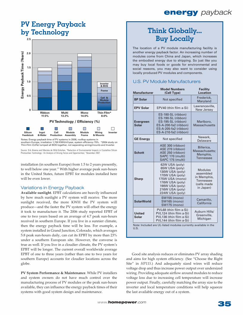
PV Technology / Efficiency (%)
Ener
gy P
ayba
ck T
ime
(Yea
rs)
0
0.5
1.0
1.5
2.0
2.5
Ribbon11.5%
Multi13.2%
Mono14.0%
Thin-Film*8.0%
SiliconFeedstock
Ingot & Wafer
Cell Production
Module Assembly
Module Frame
Frame
Wiring & Mounts
Inverter
Inverter& BOS
Notes: Energy payback time of PV systems in 2006, rooftop systems in southern Europe, irradiation 1,700 KWH/m2/year, system efficiency 75%. *2004 study on Thin-Film (CdTe) lumped all BOS together, not separating wiring/mounts and Inverter.
Cell & Module
Production
Good site analysis reduces or eliminates PV array shading and aims for high system efficiency. (See “Choose the Right Site” in HP115.) And adequately sized wires will reduce voltage drop and thus increase power output over undersized wiring. Providing adequate airflow around modules to reduce voltage loss due to increasing cell temperature will increase power output. Finally, carefully matching the array size to the inverter and local temperature conditions will help squeeze the last available energy out of a system.
PV Energy Payback by Technology
Source: Erik Alsema and Mariska de Wild-Scholten, “Reduction of Environmental Impacts in Crystalline Silicon Photovoltaic Technology– An Analysis of Driving Forces and Opportunities,” November 2007.
Systems also require periodic maintenance. Trim growing trees or shrubs that may start to shade the array. Keeping modules dust- and debris-free will help keep performance at its peak. A quick system output check can confirm that all is in good working order. (For tips on maximizing PV system perfor mance, see “Pump Up the Power” in this issue.) Keeping your PV system in optimal working order will minimize PV system energy payback time, decrease the use of fossil fuels and associated CO2 production, and reduce the money you will need to spend on utility power or backup generator fuel.
Conventional Power vs. PVElectricity derived from coal and natural gas will never be able to outweigh the energy and continual resources required to produce it. Additionally, there are the associated environmental impacts of global warming and air, water, and soil pollution due to the emissions from fossil-fuel based power plants, and the environmental impacts of mining, drilling, and transporting coal and natural gas.
Unlike conventional energy sources, PV systems produce clean electricity for decades after achieving their energy payback in three or fewer years—this is truly the magic of PV technology.
AccessJustine Sanchez ([email protected]), is a NABCEP-certified PV installer, Home Power technical editor, and Solar Energy International instructor. Justine lives, works, and teaches from an on-grid PV-powered home in Paonia, Colorado. Her multicrystalline PV modules fully paid back their embodied energy eight months ago.
Resources:Alsema, Erik & Mariska de Wild-Scholten. 26–27 November 2007. “Reduction of Environmental Impacts in Crystalline Silicon Photovoltaic Technology—An Analysis of Driving Forces and Opportunities.” Materials Research Society, Fall 2007 meeting, Symposium R, Boston.
“PV Payback,” Karl Knapp & Theresa Jester, HP80
Thanks to Erik Alsema, Karl Knapp, and project CrystalClear (www.ipcrystalclear.info) for their help and resources.
home power 127 / october & november 200836
energy payback
Electricity derived from coal and natural gas will never be able to outweigh the energy and continual resources required to produce it.