pwm doubler with output monitoring feature · isl6617a 2 fn7844.0 december 19, 2014 submit document...
TRANSCRIPT

DATASHEET
PWM Doubler with Output Monitoring FeatureISL6617AThe ISL6617A utilizes Intersil’s proprietary Phase Doubler scheme to modulate two-phase power trains with single PWM input. It doubles the number of phases that 3.3V multiphase controllers can support.
The ISL6617A is designed to minimize the number of analog signals that interface between the controller and drivers in high phase count scalable applications. The common COMP signal, which is usually seen in conventional cascaded configurations, is not required; this improves noise immunity and simplifies the layout. Furthermore, the ISL6617A provides low part count and low cost advantage over the conventional cascaded technique.
By cascading the ISL6617A with another ISL6617 or ISL6611A, it can quadruple the number of phases that 3.3V multiphase controllers can support.
The ISL6617A also features tri-state input and outputs that recognize a high-impedance state, working together with Intersil multiphase PWM controllers and driver stages to prevent negative transients on the controlled output voltage when operation is suspended. This feature eliminates the need for the Schottky diode that may be utilized in a power system to protect the load from excessive negative output voltage damage.
Applications• High current low voltage DC/DC converters
• High frequency and high efficiency VRM and VRD
• High phase count and phase shedding applications
• 3.3V PWM input integrated power stage or DrMOS
Features• Proprietary phase doubler scheme
• Enhanced light to full load efficiency
• Double or quadruple phase count
• Patented current balancing with DCR current sensing and adjustable gain
• Current monitoring output (IOUT) to simplify system interface and layout
• Triple-level enable input for mode selection
• Dual PWM output drives for two synchronous rectified bridges with single PWM input
• Channel synchronization and two interleaving options
• Support 3.3V PWM input
• Support 5V PWM output
• Tri-state PWM input and outputs for output stage shutdown
• Overvoltage protection
• Dual flat no-lead (DFN) package
- Near chip-scale package footprint; improves PCB utilization, thinner profile
- Pb-free (RoHS compliant)
Related Literature• TB363, “Guidelines for Handling and Processing Moisture
Sensitive Surface Mount Devices (SMDs)”
Phase Doubler Selection GuidePART
NUMBERPWM INPUT
PWM OUTPUT
INTEGRATED DRIVER CASCADED DEVICES COMPATIBLE CONTROLLERS
ISL6617 5.0V 5.0V N/A 5.0V PWM DrMOS; ISL6617, ISL6611A
ISL6336G, ISL6372/3/4/5/6, ISL6364/67/67H; ISL6388/98 with 5V PWM Option
ISL6617A 3.3V 5.0V N/A 5.0V PWM DrMOS; ISL6617, ISL6611A
3.3V PWM Digital Controllers with Phase Doubler Compatibility; ISL6388/98 with 3.3V PWM Option
ISL6611A 5V N/A 5.0V Discrete MOSFET; Dual FETS
ISL6336G, ISL6372/3/4/5/6, ISL6364/67/67H; ISL6388/98 with 5V PWM Option
1 CAUTION: These devices are sensitive to electrostatic discharge; follow proper IC Handling Procedures.1-888-INTERSIL or 1-888-468-3774 | Copyright Intersil Americas LLC 2014. All Rights Reserved
Intersil (and design) is a trademark owned by Intersil Corporation or one of its subsidiaries.All other trademarks mentioned are the property of their respective owners.
December 19, 2014FN7844.0

ISL6617A
Internal Block Diagram
VCC
PWMIN
10k
5.5k CSRTNA
PWMA
GND
PWMB
CSENB
CSRTNB
CHANNEL A
CHANNEL B
EN_SYNC
CURRENT BALANCE BLOCK
CSENA
CONTROLLOGIC
IOUT
Ordering InformationPART NUMBER(Notes 1, 2, 3)
PARTMARKING
TEMP. RANGE(°C)
PACKAGE(RoHS Compliant)
PKG.DWG. #
ISL6617AFRZ 17AF -40 to +125 10 Ld 3x3 DFN L10.3x3
NOTES:
1. Add “-T*” suffix for tape and reel. Please refer to TB347 for details on reel specifications.
2. These Intersil Pb-free plastic packaged products employ special Pb-free material sets, molding compounds/die attach materials, and 100% matte tin plate plus anneal (e3 termination finish, which is RoHS compliant and compatible with both SnPb and Pb-free soldering operations). Intersil Pb-free products are MSL classified at Pb-free peak reflow temperatures that meet or exceed the Pb-free requirements of IPC/JEDEC J STD-020.
3. For information on MSL please see techbrief TB363.
2 FN7844.0December 19, 2014
Submit Document Feedback

ISL6617A
Pin ConfigurationISL6617A
(10 LD DFN)TOP VIEW
1
3
4
PWMIN
CSENA VCC
CSRTNA
2
10
8
7
9
PWMA
IOUT
EN_SYNC
GND
11
5 6 PWMBCSENB
CSRTNB
Functional Pin DescriptionsPIN # PIN SYMBOL FUNCTION
1 CSRTNA Output of the differential amplifier for Channel A. Connect a resistor on this pin to the negative rail of the sensed voltage to set the current gain.
2 CSENA Input of the differential amplifier for Channel A. Typically, the positive rail of sensed voltage via DCR sensing network connects to this node.
3 PWMIN The PWM input signal (3.3V) triggers the J-K flip flop and alternates its input to Channel A and B. Both channels are effectively modulated. The PWM signal can enter three distinct states during operation; see “Operation” on page 8 for further details. Connect this pin to the PWM output of the controller.
4 CSRTNB Output of the differential amplifier for Channel B. Connect a resistor on this pin to the negative rail of the sensed voltage to set the current gain.
5 CSENB Input of the differential amplifier for Channel B. Typically, the positive rail of sensed voltage via DCR sensing network connects to this node.
6 PWMB PWM output of Channel B with 5V PWM tri-state compatibility.
7 EN_SYNC Driver Enable and Mode Selection Input. See “EN_SYNC Operation” on page 8 for more details.
8 IOUT Current monitoring Output. It sources out the average current of both Channel A and B.
9 VCC Connect this pin to a +5V bias supply. It supplies power to internal analog circuits. Place a high quality low ESR ceramic capacitor from this pin to GND.
10 PWMA PWM output of Channel A with 5V PWM tri-state compatibility.
11 GND Bias and reference ground. All signals are referenced to this node. Place a high quality low ESR ceramic capacitor from this pin to VCC. Connect this pad to the power ground plane (GND) via thermally enhanced connection.
3 FN7844.0December 19, 2014
Submit Document Feedback

ISL6617A
Typical Application (2-Phase Controller for 4-Phase Operation)
MAINCONTROLISL69xxx
+5V
VSEN
GND
VCC
VR_RDY
CS0EN
ISL6617A
GND
VCC
EN_SYNC
IOUT
PWM0
+VCORE
CSRTN0
PWMIN
+3.3V
CS1
PWM1
CSRTN1
+5V
+12V
GND
VIN
PHASEPWM
+12V
GND
VIN
PHASEPWMPWMB
PWMA
CSENA
CSRTNACSRTNB
CSENB
+5V
ISL6617A
GND
VCC
EN_SYNC
IOUT
PWMIN
+5V
+12V
GND
VIN
PHASEPWM
+12V
GND
VIN
PHASEPWMPWMB
PWMA
CSENA
CSRTNACSRTNB
CSENB
POWER STAGE
POWER STAGE
POWERSTAGE
POWERSTAGE
4 FN7844.0December 19, 2014
Submit Document Feedback

ISL6617A
Typical Application II (2-Phase Controller to 8-Phase Operation)
MAINCONTROLISL69xxx
VSEN
GND
VCC
CS0
PWM0
+VCORE
CSRTN0
+3.3V
CS1
PWM1
CSRTN1
+5V
ISL6617
GND
VCC
EN_SYNC
IOUT
PWMIN
+5V+12V
GND
VIN
PHASEPWM
+12V
GND
VIN
PHASEPWMPWMB
PWMA
ISENA-
ISENA+ISENB+
ISENB-
+5V
ISL6617
GND
VCC
EN_SYNC
IOUT
PWMIN
+5V
+12V
GND
VIN
PHASEPWM
+12V
GND
VIN
PHASEPWMPWMB
PWMA
ISENA-
ISENA+ISENB+
ISENB-
+5V
ISL6617A
GND
VCC
EN_SYNC
IOUT
PWMIN
+5V
PWMB
PWMA
CSENA
CSRTNA
CSENB
CSRTNB
POWER STAGE
POWER STAGE
+5V
ISL6617
GND
VCC
EN_SYNC
IOUT
PWMIN
+5V
+12V
GND
VIN
PHASEPWM
+12V
GND
VIN
PHASEPWMPWMB
PWMA
ISENA-
ISENA+ISENB+
ISENB-
+5V
ISL6617
GND
VCC
EN_SYNC
IOUT
PWMIN
+5V
+12V
GND
VIN
PHASEPWM
+12V
GND
VIN
PHASEPWMPWMB
PWMA
ISENA-
ISENA+ISENB+
ISENB-
+5V
ISL6617A
GND
VCC
EN_SYNC
IOUT
PWMIN
+5V
PWMB
PWMA
CSENA
CSRTNA
CSENB
CSRTNB
POWER STAGE
POWER STAGE
POWERSTAGE
POWERSTAGE
POWERSTAGE
POWERSTAGE
5 FN7844.0December 19, 2014
Submit Document Feedback

ISL6617A
Absolute Maximum Ratings Thermal InformationSupply Voltage (VCC) . . . . . . . . . . . . . . . . . . . . . . . . . . . . . . . . . -0.3V to 6.7VInput Voltage (VENx, VPWMIN, ISENx). . . . . . . . . . . . . . . -0.3V to VCC + 0.3VAmbient Temperature Range . . . . . . . . . . . . . . . . . . . . . . .-40°C to +125°CESD Rating
Human Body Model (JEDEC Class 2) . . . . . . . . . . . . . . . . . . . . . . . . . . 2kVMachine Model (JEDEC Class B) . . . . . . . . . . . . . . . . . . . . . . . . . . . . 200VCharged Device Model (JEDEC Class IV) . . . . . . . . . . . . . . . . . . . . . . . 2kV
Latch-up (JEDEC Class II) . . . . . . . . . . . . . . . . . . . . . . . . . . . . . . . . . . . .+85°C
Thermal Resistance (Typical) JA(°C/W) JC(°C/W)10 Ld DFN (Notes 4, 5) . . . . . . . . . . . . . . 48 7
Maximum Junction Temperature . . . . . . . . . . . . . . . . . . . . . . . . . . . .+150°CMaximum Storage Temperature Range . . . . . . . . . . . . . .-65°C to +150°CPb-Free Reflow Profile . . . . . . . . . . . . . . . . . . . . . . . . . . . . . . . . . . see TB493
Recommended Operating ConditionsAmbient Temperature . . . . . . . . . . . . . . . . . . . . . . . . . . . . .-40°C to +125°CMaximum Operating Junction Temperature . . . . . . . . . . . . . . . . . . +125°CSupply Voltage, VCC . . . . . . . . . . . . . . . . . . . . . . . . . . . . . . . . . . . . . 5V 10%
CAUTION: Do not operate at or near the maximum ratings listed for extended periods of time. Exposure to such conditions may adversely impact productreliability and result in failures not covered by warranty.
NOTES:
4. JA is measured in free air with the component mounted on a high effective thermal conductivity test board with “direct attach” features. See Tech Brief TB379.
5. JC, “case temperature” location is at the center of the package underside exposed pad.
Electrical Specifications These specifications apply for recommended ambient temperature, unless otherwise noted. Boldface limits apply over the operating temperature range.
PARAMETER SYMBOL TEST CONDITIONSMIN
(Note 6) TYPMAX
(Note 6) UNITS
SUPPLY CURRENT
Bias Supply Current IVCC PWM pin floating, VVCC = 5V, EN_SYNC = 5V 5 6.5 mA
PWM pin floating, VVCC = 5V, EN_SYNC = 0V 5 6.5 mA
FPWM = 600kHz, VVCC = 5V, EN_SYNC = 5V 6 7.5 mA
FPWM = 600kHz, VVCC = 5V, EN_SYNC = 4.25V 6 7.5 mA
FPWM = 300kHz, VVCC = 5V, EN_SYNC = 3.25V 6 7.5 mA
POWER-ON RESET
POR Rising 3.4 4.2 V
POR Falling 2.3 3.0 V
Hysteresis 350 mV
EN_SYNC INPUT
ENx Minimum LOW Threshold VENx 0.8 V
ENx Maximum HIGH Threshold VENx 2.0 V
SYNC AND INTERLEAVING MODE
Interleaving Mode 1 Window VENx 97% VCC
Interleaving Mode 2 Window VENx 78% 85% VCC
Synchronous Mode Window VENx 54% 64% VCC
Typical Threshold Hysteresis -5% VCC
Minimum SYNC Pulse 40 ns
Maximum Synchronization Delay 50 ns
Interleaving Mode Phase Shift SYNC = 5V, PWM = 300kHz, 10% Width 180 °
Synchronization Mode Phase Shift SYNC = 0V, PWM = 300kHz, 10% Width 0 °
PWM INPUT (PWMIN)
Sinking Impedance RPWM_SNK 5.5 kΩ
Source Impedance RPWM_SRC 10 kΩ
6 FN7844.0December 19, 2014
Submit Document Feedback

ISL6617A
Tri-State to PWM High Rising Threshold VVCC = 5V 2.50 2.70 V
Tri-State to PWM High Falling Threshold VVCC = 5V 2.00 2.25 V
Tri-State to PWM Low Rising Threshold VVCC = 5V 0.95 1.15 V
Tri-State to PWM Low Falling Threshold VVCC = 5V 0.50 0.75 V
CURRENT SENSE (CSENA, CSENB, IOUT) AND PROTECTION (IOUT)
Sensed Current Tolerance IOUT CSENA = CSENB = 0µA -6 0 6 µA
CSENA = CSENB = 20µA 14 20 26 µA
CSENA = CSENB = 50µA 43 50 57 µA
CSENA = CSENB = 100µA 90 100 110 µA
Un-Tri State Trip for OVP IOUT ENx = LOW TO HIGH, PWM = LOW 40 60 90 µA
PWM OUTPUT (PWMA AND PWMB)
Sourcing Impedance RPWM_SRC VCC = 5V, PWMIN = HIGH 30 100 200 Ω
Sink Impedance RPWM_SNK VCC = 5V, PWMIN = LOW 30 100 150 Ω
PWM Output High Level VPWMA/B VCC = 5V, PWMIN = HIGH, 2.5mA Load 4.5 V
PWM Output Low Level VPWMA/B VCC = 5V, PWMIN = LOW, 2.5mA Load 0.4 V
PWM Tri-State Level VPWMA/B VCC = 5V, EN_PH = LOW, 0.5mA Load 1.65 2.00 2.6 V
SWITCHING TIME (See Figure 1 on page 8)
PWMA/B Low to High Rise Time tR1 Unloaded, 10% to 90% 4.5 ns
PWMA/B Tri-State to High Rise Time tR2 Unloaded, 10% to 90% 4.5 ns
PWMA/B High to Low Fall Time tF1 Unloaded, 90% to 10% 4.0 ns
PWMA/B High to Tri-state Fall Time tF2 100% to 60% (3V), Assume Equivalent Loading of RC = 50kΩ*10pF = 500ns
255 ns
PWMA/B Turn-on Propagation Delay tPDH Outputs Unloaded 35 ns
PWMA/B Turn-off Propagation Delay tPDL Outputs Unloaded, excluding extension 35 ns
PWMA/B Extension tEXT ENx = VCC, IPWMA > IPWMB 70 ns
ENx = VCC, IPWMA < IPWMB 70 ns
ENx = 80%*VCC, IPWMA > IPWMB 190 ns
ENx = 80%*VCC, IPWMA < IPWMB 190 ns
Tri-State to High or Low Propagation Delay tPTS Outputs Unloaded, excluding extension 10 ns
Tri-State Shutdown Hold-off Time tTSSHD Including Propagation Delay 65 ns
NOTE:6. Parameters with MIN and/or MAX limits are 100% tested at +25°C, unless otherwise specified. Temperature limits established by characterization
and are not production tested.
Electrical Specifications These specifications apply for recommended ambient temperature, unless otherwise noted. Boldface limits apply over the operating temperature range. (Continued)
PARAMETER SYMBOL TEST CONDITIONSMIN
(Note 6) TYPMAX
(Note 6) UNITS
7 FN7844.0December 19, 2014
Submit Document Feedback

ISL6617A
Timing Diagram
OperationDesigned for high phase count and phase shedding applications, the ISL6617A driverless phase doubler is meant to double or quadruple (cascaded with two ISL6617s) the number of phases that 3.3V multiphase controllers can support.
A rising transition on PWMIN initiates the turn-on of the PWMA/B (see Figure 1). After a short propagation delay [tPDH], the PWMA/B begins to rise. Typical rise times [tR1] are provided in the “Electrical Specifications” table on page 7.
A falling transition on PWMIN indicates the turn-off of the PWMA/B. The PWMA/B begins to fall [tF1] after a propagation delay [tPDL], which is modulated by the current balance circuits.
When the PWMIN stays in the tri-state window for longer than [tTSSHD], both PWMA/B will pull to 40% of VCC so that the cascaded 5V PWM input MOSFET driver or integrated power stage can recognize tri-state.
EN_SYNC OperationThe EN_SYNC pin features multiple functions. It is the enable input of the device and the input to select various operational modes.
ENABLE OPERATION
As shown in Figure 2, the ISL6617A disables the doubler operation when the EN_SYNC pin is pulled to ground. When the EN_SYNC returns high, the phase doubler will pull the PWM line into the tri-state window, and then will be enabled only at the leading edge of the PWM input. Prior to the first PWMIN rising edge, both the PWMA and PWMB output will remain in tri-state unless an overvoltage fault is detected. This fault is defined as when a phase is detected to have more than 60% of the
maximum IOUT current. This provides additional protection to the load if the upper MOSFET experiences a short while the doubler is enabled.
The EN_SYNC pin should remain high if driving the PWM line high is prohibited for the associated controller. For proper system interface, please refer to the respective device datasheet.
SYNCHRONOUS OPERATIONThe ISL6617A can be set in interleaving mode or synchronous mode by pulling the EN_SYNC pin to the respective level, as shown in Table 1. A synchronous pulse can be sent to the phase doubler during the load application to improve the voltage droop and current balance while still maintaining interleaving operation at DC load conditions. However, excessive ringback can occur; hence, the synchronous mode operation should be carefully investigated. Figure 3 shows how to generate a synchronous pulse when a transient load is applied. The comparator should be a fast comparator with a minimum delay.
VARIOUS OPERATIONAL MODESThe ISL6617A has three distinct operating modes depending upon the voltage level of the EN_SYNC pin. To ensure that the ISL6617A is in operation, the pin must be above 2V. When the EN_SYNC pin is set to above 97% of VCC, the ISL6617A will operate in interleaving mode with a maximum extension of 70ns. When VCC is between 78% and 85% of VCC, the ISL6617A operates in interleaving mode with a fixed extension of 120ns and a variable extension of up to 70ns. This results in a minimum extension of 120ns and a max of 190ns. To enter this 2nd interleaving mode, the pin must remain in the 78% to 85% range for at least 4 cycles. Between 54% and 64% of VCC, the device operates in synchronous mode. Figures 4 and 5 show simplified synchronous and interleaving modes’ operational waveforms, respectively.
FIGURE 1. TIMING DIAGRAM
PWMIN
PWMA/B
tPDH
tR1
tPDL
10%
1.7V
tF2
tF1
tPTS
tTSSHD
tTSSHD
90%
10%90% tPTS
60%
15ns
tR2
10%
90%
3.3V
5V
FIGURE 2. TYPICAL ENABLE OPERATION TIMING DIAGRAM
EN_SYNC
PWMIN
PWMA/B
FIGURE 3. TYPICAL SYNC PULSE GENERATOR
+
-
COMP
SYNC
1.0nF
2kΩ
20kΩ49.9kΩ
1kΩ
VCC
0Ω
DNP
8 FN7844.0December 19, 2014
Submit Document Feedback

ISL6617A
To transition between two different modes, the EN_SYNC pin voltage level needs to be set accordingly. Figures 6 and 7 show an example of external circuits for mode transition between synchronous mode and interleaving #1 or #2 mode, respectively. The R should be less than 50kΩ to improve transition time.
TABLE 1. ISL6617A OPERATIONAL MODES
MODE MIN TYP MAX EXTENSION
Enable Low 0.8V
Enable High 2V
Interleaving#1 97%*VCC VCC 0ns to 70ns
Interleaving#2 78%*VCC 81%*VCC 85%*VCC 120ns + (0ns to 70ns)
Synchronous 54%*VCC 60%*VCC 64%*VCC 0ns to 70ns
Not Used From 0.8V to 2V or 54% of VCC is not recommended Region
FIGURE 4. INTERLEAVING MODE’S OPERATIONAL WAVEFORMS (ENx = VCC, OR 81%*VCC)
PWM
PWMA
PWMB
FIGURE 5. SYNCHRONOUS MODE’S OPERATIONAL WAVEFORMS (EN_SYNC = 60%*VCC)
PWM
PWMA
PWMB
FIGURE 6. CONFIGURATION FOR TRANSITION BETWEEN SYNCHRONOUS AND INTERLEAVING #1 MODES
VCC
SYNC
-
+
SYNC 0ns TO 70ns
INTERLEAVING 0ns TO 70ns
ENTTL -
+
-
+
-
+
INTERLEAVING+120+(0ns TO 70ns)
40%*R
60%*R4 CYCLES BLANKING
ISL6617A
EN_SYNC
FIGURE 7. CONFIGURATION FOR TRANSITION BETWEEN SYNCHRONOUS AND INTERLEAVING #2 MODES
VCC
SYNC
-
+
SYNC 0ns TO 70ns
INTERLEAVING0ns TO 70ns
ENTTL-
+
-
+
-
+
INTERLEAVING +120+(0ns TO 70ns)
19%*R
28.5%*R4 CYCLES BLANKING
52.5%*R
ISL6617A
EN_SYNC
9 FN7844.0December 19, 2014
Submit Document Feedback

ISL6617A
The ISL6617A can further be cascaded with ISL6617 or ISL6611A (phase doubler with integrated 5V drivers), as shown in Figure 8. This can quadruple the number of phases each PWM line can support. Figure 9 shows the operational waveforms of the cascaded doublers. The PWMIN pin of ISL6617 or ISL6611A will be pulled to VCC when it is disabled (EN_x = Low). To avoid driving the PWM outputs of the 1st stage ISL6617A by the 2nd stage’s PWMIN, the 2nd stage doubler’s enable input should remain high, i.e, tied to VCC, as shown in Figure 8. Note that ISL6617A cannot cascade with itself and its PWMIN will not be pulled to VCC when EN_x is disabled (Low).
To operate each phase at the switching frequency of fSW, the operational frequency of the controller needs to be scaled accordingly for different modes, as shown in Table 2.
When the doubler operates in interleaving mode, the PWM controller frequency should be set at two times the desired phase frequency (fSW). Since the input PWM pulse is divided into half to feed into each phase of the doubler, the operational duty cycle of each phase should be less than 50%. In synchronous mode, the PWM controller should be operated at the same frequency as the desired phase frequency. In this mode, the allowable duty cycle is up to 100%. For cascaded interleaving, the controller switching frequency needs to be set at four times the phase frequency. During cascaded operation, the maximum
allowable duty cycle will be less than 25%. All of the maximum allowable duty cycle numbers referenced assume that the PWM controller can send out a 100% duty cycle pulse. In many cases, this is not achievable because the controller needs time to reset its internal sawtooth ramp or internal max duty limit. However, the fixed 120ns extension of interleaving mode 2 helps recover the typical 1% duty cycle loss associated with the ramp reset time.
To properly compensate the system that uses phase doublers, the effective system sawtooth to calculate the modulator gain should factor in the duty cycle limitation (DMAX) as Equation 1. For instance, when using ISL6617A and ISL6617 in cascaded interleaving mode, the effective sawtooth amplitude should be scaled as 3V/22.5% = 13.33V.
FIGURE 8. CASCADED PHASE DOUBLER SIMPLIFIED DIAGRAM
PO
WE
R
ST
AG
EP
OW
ER
S
TA
GE
PO
WE
R
ST
AG
EP
OW
ER
S
TA
GE
VOUT
PWMA
PWMB
ISENA
ISENB
PWMA
PWMB
ISENA
ISENB
PWMA
PWMB
CSENA
CSENB
IOUT
IOUT
IOUT
PWMIN
PWMIN
PWMIN
TO
CO
NT
RO
LL
ER
ISL6617A
PHASE1A
PHASE1B
PHASE1C
PHASE1D
PWMA
PWMB
PWM1
ISL6617/ISL6611A
ISL6617/ISL6611A
PWM1A
PWM1B
PWM1C
PWM1D
VCC EN_X
VCC EN_X
TABLE 2. CONTROLLER FREQUENCY AND MAXIMUM DUTY CYCLE
OPERATIONAL MODES FCONTROLLER
ISL6617A MAXIMUM DUTY CYCLE PER PHASE
Interleaving 2 x fSW 50%
Synchronous fSW 100%
Cascaded Interleaving 4 x fSW 25%
FIGURE 9. CASCADED DOUBLER OPERATIONAL WAVEFORMS
PWM1
PWMA
PWMB
PWM1A
PWM1B
PWM1C
PWM1D
DO
UB
LER
#1
DO
UB
LER
#2
VRAMP_EFFECTIVE
VRAMPDMAX------------------= (EQ. 1)
10 FN7844.0December 19, 2014
Submit Document Feedback

ISL6617A
Current SensingThe ISL6617A senses current continuously for fast response. The ISL6617A supports inductor DCR sensing, or resistive sensing techniques. The associated channel current sense amplifier uses the ISEN inputs to reproduce a signal proportional to the inductor current, IL. The sensed current, ISEN, is proportional to the inductor current. The sensed current is used for current balance and load-line regulation.
The internal circuitry (shown in Figures 10 and 11) represents one channel. This circuitry is repeated for each channel in the doubler. The input bias current of the current sensing amplifier is typically 60nA; less than 5kΩ input impedance is preferred to minimize the offset error. In addition, the common mode input voltage to the amplifier should be less than VCC-3V.
INDUCTOR DCR SENSINGAn inductor’s winding is characteristic of a distributed resistance, as measured by the DCR (Direct Current Resistance) parameter. Consider the inductor DCR as a separate lumped quantity, as shown in Figure 10.
The channel current IL, flowing through the inductor, will also pass through the DCR. Equation 2 shows the s-domain equivalent voltage across the inductor VL.
A simple R-C network across the inductor extracts the DCR voltage, as shown in Figure 10.
The voltage on the capacitor VC, can be shown to be proportional to the channel current IL. See Equation 3.
If the R-C network components are selected such that the RC time constant matches the inductor time constant (RC = L/DCR), the voltage across the capacitor VC is equal to the voltage drop across the DCR, i.e., proportional to the channel current.
With the internal low-offset current amplifier, the capacitor voltage VC is replicated across the sense resistor RISEN. Therefore, the current out of ISEN+ pin, ISEN, is proportional to the inductor current.
Because of the internal filter at ISEN- pin, one capacitor, CT, is needed to match the time delay between the ISEN- and ISEN+ signals. Select the proper CT to keep the time constant of RISEN and CT (RISEN x CT) close to 27ns.
Equation 4 shows that the ratio of the channel current to the sensed current, ISEN, is driven by the value of the sense resistor and the DCR of the inductor.
RESISTIVE SENSINGFor more accurate current sensing, a dedicated resistor RSENSE in series with each output inductor can serve as the current sense element (see Figure 11). This technique reduces overall converter efficiency due to the additional power loss on the current sense element RSENSE.
The same capacitor CT is needed to match the time delay between ISEN- and ISEN+ signals. Select the proper CT to keep the time constant of RISEN and CT (RISEN x CT) close to 27ns.
Equation 5 shows the ratio of the channel current to the sensed current ISEN.
FIGURE 10. DCR SENSING CONFIGURATION
IA/B
ISEN ILDCR
RISEN---------------=
-
+CSEN(A/B)
CURRENTSENSE
VIN
CSRTN(A/B)
PWMA/B
POWER
RISEN(A/B)
DCRL
INDUCTOR
R
VOUT
COUT
-+ VC(s)
C
IL s
-+ VL
CT
ISL6617A
STAGE
VL s IL s L DCR+ = (EQ. 2)
VC s s
LDCR------------ 1+
DCR IL
s RC 1+ -----------------------------------------------------------------=
(EQ. 3)
ISEN ILDCR
RISEN---------------= (EQ. 4)
FIGURE 11. SENSE RESISTOR IN SERIES WITH INDUCTORS
IA/B
ISEN IL
RSENSERISEN
--------------------------=
CSEN(A/B)
CURRENT
SENSE
CSRT(A/B)
RISEN(A/B)
RSENSEL
VOUT
COUT
IL
CT
ISL6617A
-
+
ISEN ILRSENSERISEN
--------------------= (EQ. 5)
11 FN7844.0December 19, 2014
Submit Document Feedback

ISL6617A
Current Balance and Current MonitoringThe sensed currents IA and IB from each respective channel are summed together and divided by 2. The resulting average current IAVG provides a measure of the total load current. Channel current balance is achieved by comparing the sensed current of each channel to the average current to make an appropriate adjustment to the PWMA and PWMB duty cycle with Intersil’s patented current-balance method.
Channel current balance is essential in achieving the thermal advantage of multiphase operation. With good current balance, the power loss is equally dissipated over multiple devices and a greater area.
The resulting average current IAVG also goes out from the IOUT pin for current monitoring and can also be fed back to the controller’s ISEN lines for current balance, load-line regulation, and overcurrent protection. For fast response to the current information, the IOUT pin should have minimum decoupling; no more than 50ns filter is recommended. The full scale of IOUT is 100µA; it typically should set resistor gain around 50µA to 80µA at the full load to ensure that it will not hit the full scale prior to the overcurrent trip point. At the same time, the current signal accuracy is maximized.
Benefits of a High Phase Count SystemAt heavy load condition, efficiency can be improved by spreading the load across many phases. This is primarily because the resistive loss becomes the dominant component of total loss budget at high current levels.
Since the load is carried by more phases, each power device handles less current. In addition, the devices are likely to be spread over a larger area on the Printed Circuit Board (PCB). Both these factors result in improved heat dissipation for higher phase count systems. By reducing the system’s operating temperature, the reliability of the components is improved.
Furthermore, increasing the phase count also reduces the size of ripple on both the input and output currents. It reduces EMI and improves the efficiency. Figures 12 and 13 show the ripple values for a 24-phase voltage regulator with the following parameters:
• Input voltage: 12V
• Output voltage: 1.6V
• Duty cycle: 13.3%
• Load current: 200A
• Output Phase Inductor: 500nH
• Phase switching frequency: 200kHz
In this example, the 24-phase voltage regulator (VR) can run in 6-phase, 8-phase, 12-phase or 24-phase interleaving mode. In 6-phase interleaving mode, every 4 phases runs synchronously, which yields 18.73A and 12.93A input and output ripple currents, respectively. The 24-phase interleaving regulator significantly drops these values to 4.05A and 0.78A, respectively. As shown in Table 3, both input and output ripple currents are reduced when more phases are running in interleaving mode. Note that the 8-phase VR has lower output ripple current than the 12-phase VR since the 8-phase VR has better output ripple cancellation factor close to the duty cycle of 1/8.
Figure 14 shows the efficiency of a 12-phase VR design, which runs the doubler in interleaving and synchronous modes. For comparison, a 6-phase VR with the same number of MOSFETs and inductors is also plotted, clearly demonstrating the efficiency improvement of a high-phase count system and interleaving mode over synchronous mode resulting from the better ripple cancellation.
TABLE 3. RIPPLE CURRENT (UNIT: A)
INTERLEAVED PHASES 6 8 12 24
Input Ripple Current 18.73 11.64 8.79 4.05
Output Ripple Current 12.93 2.70 4.83 0.78
12 FN7844.0December 19, 2014
Submit Document Feedback

ISL6617A
FIGURE 12. INPUT CURRENT RIPPLE vs DUTY CYCLE, PHASE COUNT FIGURE 13. OUTPUT CURRENT RIPPLE vs DUTY CYCLE, PHASE COUNT
FIGURE 14. EFFICIENCY COMPARISON IN 12-PHASE DESIGN
24 CHANNELS, 6 INTERLEAVING
24 CHANNELS, 12 INTERLEAVING
24 INTERLEAVING PHASES
24 CHANNELS, 8 INTERLEAVING
20
15
10
5
0
INP
UT
RIP
PL
E C
UR
RE
NT
(A
)20
15
10
5
0
DUTY CYCLE (%)
0 10 20 30 40 50
24 CHANNELS, 6 INTERLEAVING
24 CHANNELS, 8 INTERLEAVING
24 CHANNELS, 12 INTERLEAVING
24 INTERLEAVING PHASES
0 10 20 30 40 50
OU
TP
UT
CU
RR
EN
T R
IPP
LE
(A
)
DUTY CYCLE (%)
80
60
40
20
0
6-PHASE, SAME AMOUNTOF MOSFETS AND INDUCTORS
PHASE DOUBLER IN SYNCHRONOUS MODE
PHASE DOUBLER ININTERLEAVING MODE
0 20 40 60 80 100 120 140 160 180LOAD (A)
93
92
91
90
89
88
87
86
85
EF
FIC
IEN
CY
(%
)
13 FN7844.0December 19, 2014
Submit Document Feedback

ISL6617A
Intersil products are manufactured, assembled and tested utilizing ISO9001 quality systems as notedin the quality certifications found at www.intersil.com/design/quality
Intersil products are sold by description only. Intersil Corporation reserves the right to make changes in circuit design, software and/or specifications at any time without notice. Accordingly, the reader is cautioned to verify that data sheets are current before placing orders. Information furnished by Intersil is believed to be accurate and reliable. However, no responsibility is assumed by Intersil or its subsidiaries for its use; nor for any infringements of patents or other rights of third parties which may result from its use. No license is granted by implication or otherwise under any patent or patent rights of Intersil or its subsidiaries.
For information regarding Intersil Corporation and its products, see www.intersil.com
For additional products, see www.intersil.com/product_tree
About IntersilIntersil Corporation is a leading provider of innovative power management and precision analog solutions. The company's products address some of the largest markets within the industrial and infrastructure, mobile computing and high-end consumer markets.
For the most updated datasheet, application notes, related documentation and related parts, please see the respective product information page found at www.intersil.com.
You may report errors or suggestions for improving this datasheet by visiting www.intersil.com/ask.
Reliability reports are also available from our website at www.intersil.com/support
Revision HistoryThe revision history provided is for informational purposes only and is believed to be accurate, but not warranted. Please go to web to make sure you have the latest Rev.
DATE REVISION CHANGE
December 19, 2014 FN7844.0 Initial Release
14 FN7844.0December 19, 2014
Submit Document Feedback
ISL6617A
15 FN7844.0December 19, 2014
Submit Document Feedback
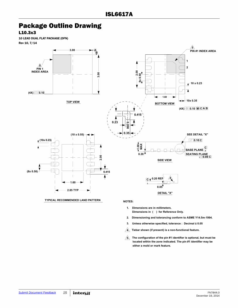
Package Outline DrawingL10.3x310 LEAD DUAL FLAT PACKAGE (DFN)
Rev 10, 7/14
located within the zone indicated. The pin #1 identifier may be
Unless otherwise specified, tolerance : Decimal ± 0.05
Tiebar shown (if present) is a non-functional feature.
The configuration of the pin #1 identifier is optional, but must be
Dimensions in ( ) for Reference Only.
Dimensioning and tolerancing conform to ASME Y14.5m-1994.
5.
either a mold or mark feature.
3.
4.
2.
Dimensions are in millimeters.1.
NOTES:
BOTTOM VIEW
DETAIL "X"
SIDE VIEW
TYPICAL RECOMMENDED LAND PATTERN
TOP VIEW
(4X) 0.10
INDEX AREAPIN 1
PIN #1 INDEX AREA
C
SEATING PLANE
BASE PLANE
0.08
SEE DETAIL "X"
C
C4
5
5AB
0.10 C
1
1.0
0
0.20
8x
0.5
02.0
0
3.0
0
(10x 0.23)
(8x 0.50)
2.0
0
1.60
(10 x 0.55)
3.00
0.05
0.20 REF
10 x 0.23
10x 0.35
1.60
MA
X
(4X) 0.10 A BCM
0.415
0.23
0.35
0.200
2
2.85 TYP
0.415