pwm2/ gnd al1791/1792/1793/1794 pwm1 4 11 led4/ · pdf fileal1791/1792/1793/1794 ... the...
TRANSCRIPT
AL1791/1792/1793/1794 Document number:37957 Rev. 3 - 2
1 of 18 www.diodes.com
September 2015 © Diodes Incorporated
AD
VA
NC
ED
IN
FO
RM
AT
IO
AL1791/1792/1793/1794
Single/Dual/Triple/Quad-Channel Current-Ratio-Optimized LED Driver with Analog and PWM Dimming
U-DFN-4030-14
Description
The AL1791/1792/1793/1794 (or collectively AL179x), a single/multi-
channel LED driver with analog and PWM dimming control, is
targeted for Tunable White/Color Smart Lighting application. It serves
as the LED driving element along with AC-DC Power Conversion
Block and Intelligent wireless MCU as an emerging smart-connected
lighting system configuration. The key merits attribute to cost-
effectiveness, dimming performance, low standby power, ease of
system implementation, and great scalability. AL1791, AL1792,
AL1793, and AL1794 are 1-channel, 2-channel, 3-channel, and 4-
channel LED drivers, respectively.
The IC is available in U-DFN-4030-14 package.
Features Input Voltage Range: 6.5V to 30V
1/2/3/4-channel LED drivers: independent Analog or PWM dimming control for each channel
Reference Current: Adjustable by an external reference resistor
Ratio-optimized currents for 4 independent LED channels (AL1794 only): Suitable for Tunable White and Tunable Color
Low Standby Power: With EN pin
E-flicker free High Frequency PWM dimming with Deep Dimming Capability: Support 10KHz down to 1.0%, 4KHz down to 0.4%, or 1KHz down to 0.1%
Internal Protections: Under Voltage Lockout (UVLO), LED string open/short protection
Over-temperature protection (OTP): Thermal shutdown and auto thermal recovery
Fault Reporting: UVLO, OTP, Open, and Short LED Power Good Reporting
Low system BOM cost
Ambient Temperature Range -40°C to +125°C
U-DFN4030-14: Available in “Green” Molding Compound (No Br, Sb)
Totally Lead-Free & Fully RoHS Compliant (Notes 1 & 2)
Halogen and Antimony Free. “Green” Device (Note 3)
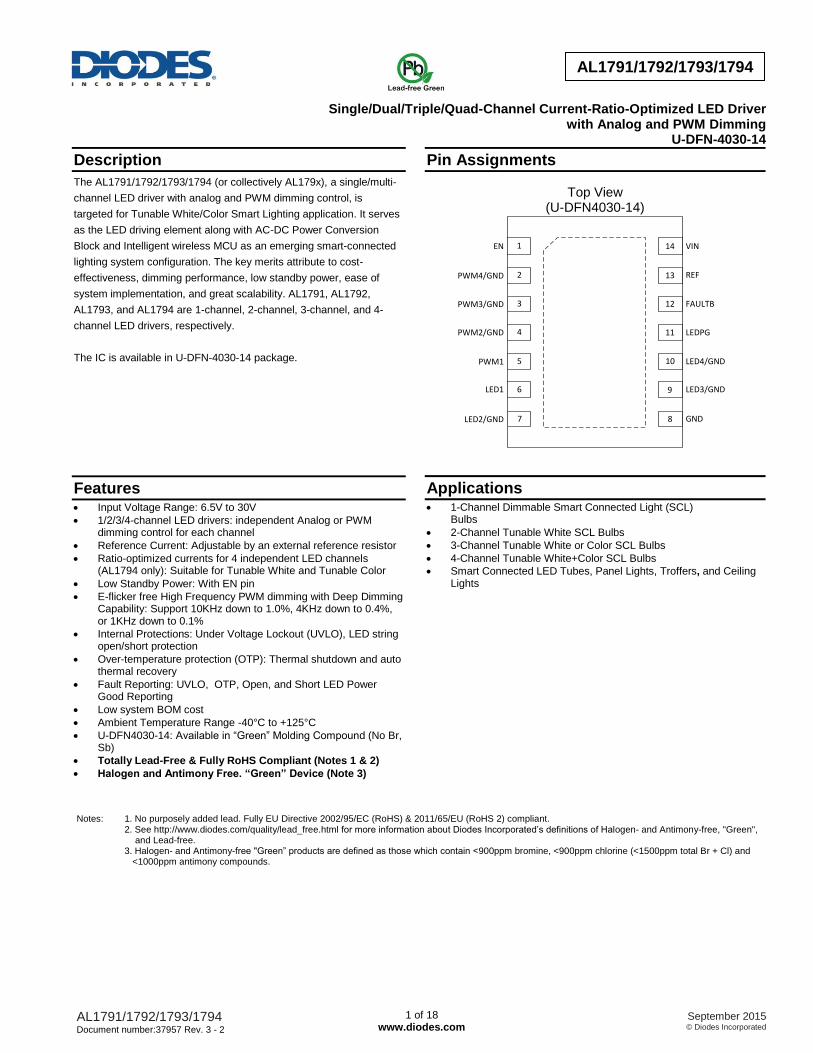
Pin Assignments
Top View (U-DFN4030-14)
Applications 1-Channel Dimmable Smart Connected Light (SCL)
Bulbs
2-Channel Tunable White SCL Bulbs
3-Channel Tunable White or Color SCL Bulbs
4-Channel Tunable White+Color SCL Bulbs
Smart Connected LED Tubes, Panel Lights, Troffers, and Ceiling Lights
Notes: 1. No purposely added lead. Fully EU Directive 2002/95/EC (RoHS) & 2011/65/EU (RoHS 2) compliant. 2. See http://www.diodes.com/quality/lead_free.html for more information about Diodes Incorporated’s definitions of Halogen- and Antimony-free, "Green",
and Lead-free. 3. Halogen- and Antimony-free "Green” products are defined as those which contain <900ppm bromine, <900ppm chlorine (<1500ppm total Br + Cl) and
<1000ppm antimony compounds.
EN
PWM4/GND
PWM3/GND
PWM2/GND
PWM1
LED1
LED2/GND
VIN
REF
FAULTB
LEDPG
LED4/GND
LED3/GND
GND
1
2
3
4
5
6
7 8
9
10
11
12
13
14

AL1791/1792/1793/1794 Document number:37957 Rev. 3 - 2
2 of 18 www.diodes.com
September 2015 © Diodes Incorporated
AD
VA
NC
ED
IN
FO
RM
AT
IO
AL1791/1792/1793/1794
Typical Applications Circuit
Figure 1. 1-Channel Dimmable White
Figure 2. 2-Channel Tunable White
ENPWM1PWM2PWM3
FAULTB
REF
GND
LED1LED2
LED3
3.3VRFAULT
RSET
VIN
VLED1
Wireless/Color management
MCU
AP3983CAC-DC
Conversion
85~265Vac
AL1794
LEDPG
RLEDPG
VIN adjustment signal
VLED2
G R B
LED4
PWM4
Figure 3. 3-Channel Tunable Color
ENPWM1
FAULTB
REF
GND
LED13.3V
RFAULT
RSET
VIN
VLED1
Wireless/Color management
MCU
AP3983CAC-DC
Conversion
85~265Vac
AL1791
LEDPG
RLEDPG
VIN adjustment signal
2700K
X8
ENPWM1PWM2
FAULTB
REF
GND
LED1LED2
3.3VRFAULT
RSET
VIN
VLED1
Wireless/Color management
MCU
AP3983CAC-DC
Conversion
85~265Vac
AL1792
LEDPG
RLEDPG
VIN adjustment signal
2700K
X8
6500K
X8
AL1791/1792/1793/1794 Document number:37957 Rev. 3 - 2
3 of 18 www.diodes.com
September 2015 © Diodes Incorporated
AD
VA
NC
ED
IN
FO
RM
AT
IO
AL1791/1792/1793/1794
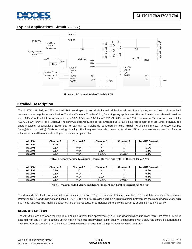
Typical Applications Circuit (continued)
ENPWM1PWM2PWM3
FAULTB
REF
GND
LED1LED2
LED3
3.3VRFAULT
RSET1
VIN
VLED1
Wireless/Color management
MCU
AP3983CAC-DC
Conversion
85~265Vac
AL1793
LEDPG
RLEDPG
VIN adjustment signal
VLED2
G R B
ENPWM1
FAULTB
REF
GND
LED1
VIN
AL1791
LEDPG
W
RSET2
Figure 4. 4-Channel White+Tunable RGB
Detailed Description
The AL1791, AL1792, AL1793, and AL1794 are single-channel, dual-channel, triple-channel, and four-channel, respectively, ratio-optimized
constant-current regulators optimized for Tunable White and Tunable Color, Smart Lighting applications. The maximum current channel can drive
up to 500mA with a total driving current up to 1.0A, 1.5A, and 1.5A for AL1792, AL1793, and AL1794 respectively. The maximum current for
AL1791 is 1A (refer to Table 1 below). The minimum channel current is recommended as in Table 2 in order to meet channel current accuracy and
short protection specifications. Each channel can still be individually controlled by either digital PWM dimming down to 0.10%@1KHz,
0.4%@4KHz, or 1.0%@10KHz or analog dimming. The integrated low-side current sinks allow LED common-anode connections for cost
effectiveness or different anode voltages for efficiency optimization.
AL179x Channel 1 Channel 2 Channel 3 Channel 4 Total IC Current
AL1791 1.0A X X X 1.0A
AL1792 0.5A 0.5A X X 1.0A
AL1793 0.5A 0.5A 0.5A X 1.5A
AL1794 0.5A 0.5A 0.375A 0.125A 1.5A
Table 1 Recommended Maximum Channel Current and Total IC Current for AL179x
AL179x Channel 1 Channel 2 Channel 3 Channel 4 Total IC Current
AL1791 0.2A X X X 0.2A
AL1792 0.1A 0.1A X X 0.2A
AL1793 0.1A 0.1A 0.1A X 0.3A
AL1794 0.1A 0.1A 0.075A 0.025A 0.3A
Table 2 Recommended Minimum Channel Current and Total IC Current for AL179x
The device detects fault conditions and reports its status on FAULTB pin. It features LED open detection, LED short detection, Over-Temperature
Protection (OTP), and Undervoltage Lockout (UVLO). The AL179x provides supreme current matching between channels and devices. Along with
bus-mode fault reporting, multiple devices can be employed together to increase current driving capability or channel count versatility.
Enable and Soft-Start
The AL179x is enabled when the voltage at EN pin is greater than approximately 2.5V, and disabled when it is lower than 0.4V. When EN pin is
asserted high and VIN pin is ramped up beyond minimum operation voltage, a soft-start will be performed with a slew-rate-controlled current ramp
over 100μS at LEDx output pins to minimize current overshoot through LED strings for optimal system reliability.
AL1791/1792/1793/1794 Document number:37957 Rev. 3 - 2
4 of 18 www.diodes.com
September 2015 © Diodes Incorporated
AD
VA
NC
ED
IN
FO
RM
AT
IO
AL1791/1792/1793/1794
Detailed Description (continued) LED Current Setting and Current Ratio
The AL1792 and AL1793 are designed to have an equal-sized channel current ratio for all channels, while the AL1794 is equipped with ratio-
optimized current sinks. The current ratio is predetermined and facilitated for Tunable Color or Tunable White applications. The absolute current
levels can be adjusted externally with RSET resistor. The LED current is expressed as below:
For AL1791:
For AL1792:
For AL1793:
For AL1794:
For example, when an RSET of 12KΩ is used, Channel 1, 2, 3, and 4 of AL1794 provide a current of 250mA, 250mA, 187.5mA, and 62.5mA
respectively. For the same RSET setting, each channel of AL1792 and AL1793 provides same current amount of 250mA. AL1791 provides 500mA
for the same RSET setting.
The maximum LED current for Channel 1 can be adjusted up to 500mA via RSET resistor. The other channels will provide current levels with the
same predetermined ratio. Any two or more channels can be tied together to drive one LED string with aggregated current. So when current
needed for any channel is greater than the maximum value the device can provide, two or more channels or devices can be paralleled together to
provide the drive current needed.
PWM Dimming Control
When any one of the PWMx pins is connected to PWM signals with frequency ranging from 500Hz and above during startup, the device is
determined in PWM dimming mode. In this mode, a high level of PWM signal will turn on the current sink to flow through the LED and low level will
turn it off. Consequently, the LED current and LED brightness of each corresponding channel can be adjusted.
The pulse width of the PWM signal is recommended to be greater than 2.5μS to support down to 0.25%@1KHz deep dimming capability still with
good linearity. Further deeper dimming through higher frequency PWM signals is possible, which maintains reasonable linearity - 0.1%@1KHz,
0.4%@4KHz, or 1.0%@10KHz. PWM signals can be driven static low or high to turn off or on the corresponding channels constantly.

AL1791/1792/1793/1794 Document number:37957 Rev. 3 - 2
5 of 18 www.diodes.com
September 2015 © Diodes Incorporated
AD
VA
NC
ED
IN
FO
RM
AT
IO
AL1791/1792/1793/1794
Detailed Description (cont.)
Analog Dimming Control
With the same PWMx pins, analog dimming can be facilitated to control the brightness of each LED channel. When no PWM signal with frequency
ranging from 500Hz and above during startup is present at PWMx pins, the device is determined in analog dimming mode. In this mode, the
signals at PWMx pins are interpreted as analog dimming signals. The meaningful dimming voltage should range from 0.4V to 1.5V. When the
voltage is 0.4V or below, the current-sink turns off the LED string. When the voltage is 1.5V or above, it turns the current level on to 100%. For any
voltage between 0.4V to 1.5V, the current level is linearly prorated to its full scale.
Undervoltage Lockout
The Undervoltage lockout function (UVLO) guarantees that the device is initially off during start-up. The UVLO functions only when the device is
enabled. Even if the AL179x is enabled, the device is not turned ON until the power supply has reached 6.3V. Whenever the input voltage falls
below approximately 6V, the device is turned off. The UVLO circuit has a hysteresis of 300mV. During UVLO, a FAULTB status will be reported.
Over-Temperature Protection
Thermal protection prevents the IC from damage when the die temperature exceeds safe margins. The AL1791/1792/1793/1794 features Over-
Temperature Protection (OTP). When the junction temperature reaches +160°C, the device will enter thermal shutdown mode in which all current
sinks are shut down and no current flows to the LED strings. The normal current level can be automatically restored to its set current from OTP by
triggering a Soft Start when the temperature lowers down below +100°C. Thermal Shut Mode will also be reported as a FAULTB.
LED Open and Short Protection
AL179x detects the LED status by continuously monitoring the current and voltage status of the LED strings. When an abnormal condition occurs
(LED Open or LED Short), FAULTB is asserted low. In the case of LED Short, all output channels will be turned off. In the case of LED Open, all
non-affected channels remain in the normal operating condition.
Fault Reporting
Fault reporting serves as a good communication channel between LED drivers and intelligent MCU unit. AL179x detects and reports the FAULTB
status upon the occurrence of Thermal Shutdown in OTP, LED Short, LED Open, and UVLO. FAULTB pin is an open-drain output design. Multiple
devices can share a single FAULTB signal by connecting all FAULTB pins together with an external pull-up resistor. Any FAULTB assertion from
any device pulls the signal down and informs MCU of the faulty condition.
LED Power Good Reporting
The Input Voltage to drive all attached Emitter Strings needs to maintain voltage level over required total VF of emitter string plus a minimum
voltage headroom (VLED_REG). On the other hand, excessive voltage headroom provided needs to be absorbed by AL179x, which increases
heat dissipation to complicate thermal management. Power Good reporting serves as a mechanism to detect the LED power supply condition and
adjusts the supply voltage to LEDs through MCU in order to minimize unnecessary overdrive voltage to the regulator and optimize the efficiency.
AL179x constantly detects and reports VLEDx (voltage measured at Pin LEDx) output headroom condition by asserting LEDPG pin. If the VLEDx in
any channel is lower than or close to the dropout voltage required by the regulator (VLED_REG) while the channel is enabled with PWMx and EN,
LEDPG pin will be pulled down to ground. During PWMx low period, internal LEDPG will not report insufficient headroom for that channel. Internal
LED Power Good logics are ANDed together before brought out to the pin. Any channel’s insufficient headroom condition will trigger a logic Low at
LEDPG pin. This signal can then be used by MCU to wisely adjust the LED power and thus the voltages to the LEDx pins to minimize power
consumption on AL179x. LEDPG needs to be connected with an external pull-up resistor. Multiple AL179x devices can also share a single pull-up
resistor to create a unified LEDPG signal.
AL1791/1792/1793/1794 Document number:37957 Rev. 3 - 2
6 of 18 www.diodes.com
September 2015 © Diodes Incorporated
AD
VA
NC
ED
IN
FO
RM
AT
IO
AL1791/1792/1793/1794
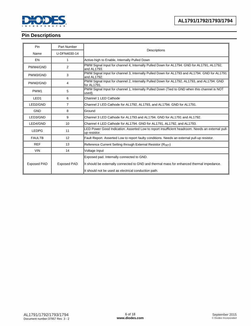
Pin Descriptions
Pin Part Number Descriptions
Name U-DFN4030-14
EN 1 Active-high to Enable, Internally Pulled Down
PWM4/GND 2 PWM Signal Input for channel 4, Internally Pulled Down for AL1794. GND for AL1791, AL1792, and AL1793.
PWM3/GND 3 PWM Signal Input for channel 3, Internally Pulled Down for AL1793 and AL1794. GND for AL1791 and AL1792.
PWM2/GND 4 PWM Signal Input for channel 2, Internally Pulled Down for AL1792, AL1793, and AL1794. GND for AL1791.
PWM1 5 PWM Signal Input for channel 1, Internally Pulled Down (Tied to GND when this channel is NOT used).
LED1 6 Channel 1 LED Cathode
LED2/GND 7 Channel 2 LED Cathode for AL1792, AL1793, and AL1794. GND for AL1791.
GND 8 Ground
LED3/GND 9 Channel 3 LED Cathode for AL1793 and AL1794. GND for AL1791 and AL1792.
LED4/GND 10 Channel 4 LED Cathode for AL1794. GND for AL1791, AL1792, and AL1793.
LEDPG 11 LED Power Good Indication. Asserted Low to report insufficient headroom. Needs an external pull-up resistor.
FAULTB 12 Fault Report. Asserted Low to report faulty conditions. Needs an external pull-up resistor.
REF 13 Reference Current Setting through External Resistor (RSET)
VIN 14 Voltage Input
Exposed PAD Exposed PAD
Exposed pad. Internally connected to GND.
It should be externally connected to GND and thermal mass for enhanced thermal impedance.
It should not be used as electrical conduction path.
AL1791/1792/1793/1794 Document number:37957 Rev. 3 - 2
7 of 18 www.diodes.com
September 2015 © Diodes Incorporated
AD
VA
NC
ED
IN
FO
RM
AT
IO
AL1791/1792/1793/1794
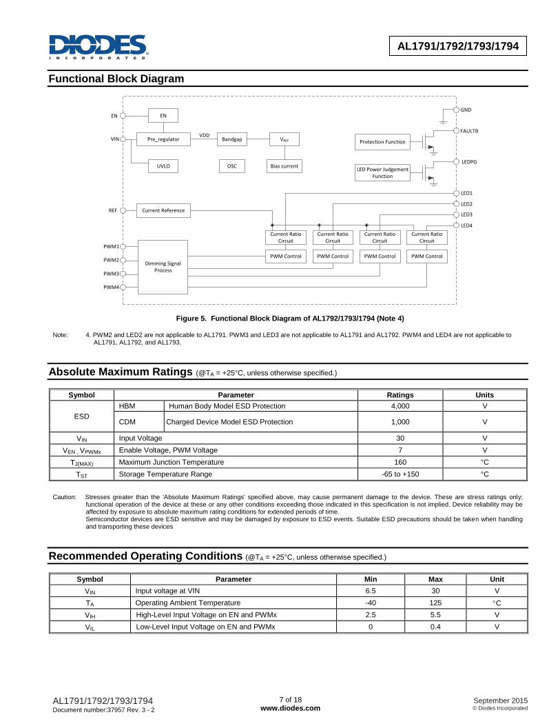
Functional Block Diagram
Figure 5. Functional Block Diagram of AL1792/1793/1794 (Note 4)
Note: 4. PWM2 and LED2 are not applicable to AL1791. PWM3 and LED3 are not applicable to AL1791 and AL1792. PWM4 and LED4 are not applicable to AL1791, AL1792, and AL1793.
Absolute Maximum Ratings (@TA = +25°C, unless otherwise specified.)
Symbol Parameter Ratings Units
ESD
HBM Human Body Model ESD Protection 4,000 V
CDM Charged Device Model ESD Protection 1,000 V
VIN Input Voltage 30 V
VEN , VPWMx Enable Voltage, PWM Voltage 7 V
TJ(MAX) Maximum Junction Temperature 160 °C
TST Storage Temperature Range -65 to +150 °C
Caution: Stresses greater than the 'Absolute Maximum Ratings' specified above, may cause permanent damage to the device. These are stress ratings only; functional operation of the device at these or any other conditions exceeding those indicated in this specification is not implied. Device reliability may be affected by exposure to absolute maximum rating conditions for extended periods of time.
Semiconductor devices are ESD sensitive and may be damaged by exposure to ESD events. Suitable ESD precautions should be taken when handling and transporting these devices
Recommended Operating Conditions (@TA = +25°C, unless otherwise specified.)
Symbol Parameter Min Max Unit
VIN Input voltage at VIN 6.5 30 V
TA Operating Ambient Temperature -40 125 C
VIH High-Level Input Voltage on EN and PWMx 2.5 5.5 V
VIL Low-Level Input Voltage on EN and PWMx 0 0.4 V
Pre_regulator Bandgap
Bias currentUVLO
EN
OSC
VREF
Dimming Signal Process
Protection Function
REF
PWM1
PWM2
PWM3
PWM4
EN
VIN
LED1
LED2
LED3
LED4
FAULTB
GND
VDD
Current Reference
Current Ratio Circuit
PWM Control
Current Ratio Circuit
PWM Control
Current Ratio Circuit
PWM Control
Current Ratio Circuit
PWM Control
LED Power Judgement Function
LEDPG

AL1791/1792/1793/1794 Document number:37957 Rev. 3 - 2
8 of 18 www.diodes.com
September 2015 © Diodes Incorporated
AD
VA
NC
ED
IN
FO
RM
AT
IO
AL1791/1792/1793/1794
Electrical Characteristics (@TA = +25°C, VIN = +12V, unless otherwise specified.)
Symbol Parameter Test Conditions Min Typ Max Unit
VUVLO UVLO Voltage VIN Rising — 6.3 — V
VUVHYS UVLO Hysteresis VIN Falling — 300 — mV
ISHDN Shutdown Supply Current Disabled — 10 — µA
IQ Quiescent Supply Current Enabled, LEDx floating, PWMx are “L”, RSET is 12KΩ — 2 — mA
VIL(EN) EN Low Voltage — 0 — 0.4 V
VIH(EN) EN High Voltage — 2.5 — — V
I(EN-PD) EN Internal Pulldown VEN=5V 0.35 — 3.5 μA
VIL(PWMx) Digital PWM Low Voltage — — — 0.3 V
VIH(PWMx) Digital PWM High Voltage — 2.5 — — V
FPWMx Digital PWM Frequency — 0.5 — 4 KHz
I(PWMx-PD) PWM Internal Pulldown VEN=5V 0.35 — 3.5 μA
TPWMx_MIN.
ON Minimum PWMx On Time — — 2.5 — μS
VADIM_MIN Analog Dimming Min Voltage — — 0.4 — V
VADIM_MAX Analog Dimming Max Voltage — — 1.5 — V
VREF Reference Voltage — 1.47 1.5 1.53 V
IREF Reference Current RSET=12KΩ — 0.125 — mA
ILED1_NOM Regulation Current for Channel 1 RSET=12KΩ — 250 — mA
ILED2_NOM Regulation Current for Channel 2 RSET=12KΩ — 250 — mA
ILED3_NOM Regulation Current for Channel 3 (not for AL1792)
RSET=12KΩ — 187.5 — mA
ILED4_NOM Regulation Current for Channel 4 (not for AL1792/1793)
RSET=12KΩ — 62.5 — mA
VLED_REG Minimum LED Regulation Voltage ILED1=250mA — 250 — mV
ILED_LEAK LEDx Leakage Current VPWMx=0V, VLEDx=+12V — 0.1 2 μA
ILED_ACCURA
CY LED Current Accuracy RSET=12KΩ -4.0 — 4.0 %
VLEDSHP LED Short Protection Threshold — — 6 — V
TLEDSHDG
Short-detection Deglitch
Analog Dimming — 2 — mS
NLEDSHDG PWM Dimming (count the number of continuous cycles when LED short is detected)
— 6 — Cycles
TLEDOPDG
Open-detection Deglitch
Analog Dimming — 2 — mS
NLEDOPDG PWM Dimming (count the number of continuous cycles when LED open is detected)
— 6 — Cycles
TSS Soft-start Time VEN=5V, 90% of ILEDx_NOM — 100 — μS
TSHDN Thermal Shutdown Threshold RSET=12KΩ — 160 — °C
TREC Thermal Recovery Threshold RSET=12KΩ — 100 — °C
VFOL FAULTB Output Low Voltage IFAULTB=1mA — — 180 mV
IFOH FAULTB Leakage Current VFAULTB=6V — — 1 μA
θJA Thermal Resistance Junction-to-Ambient
U-DFN4030-14 (Note 5) — 55 — °C/W
θJC Thermal Resistance Junction-to-Case
U-DFN4030-14 (Note 5) — 12 — °C/W
Note: 5. Device mounted on 2” x 2” FR-4 substrate PCB, 2oz copper, with minimum recommended pad on top layer and thermal vias to bottom layer ground plane.
AL1791/1792/1793/1794 Document number:37957 Rev. 3 - 2
9 of 18 www.diodes.com
September 2015 © Diodes Incorporated
AD
VA
NC
ED
IN
FO
RM
AT
IO
AL1791/1792/1793/1794
Typical Performance Characteristics (VIN=12V, RSET=12KΩ, RFAULT=10KΩ, TA=+25°C, unless otherwise specified.)
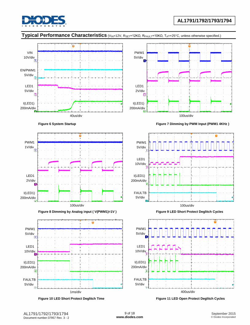
Figure 6 System Startup Figure 7 Dimming by PWM Input (PWM1 4KHz )
Figure 8 Dimming by Analog input ( V(PWM1)=1V ) Figure 9 LED Short Protect Deglitch Cycles
Fig. 5 SCP deglitch time Fig. 6 OCP deglitch cycles
Figure 10 LED Short Protect Deglitch Time Figure 11 LED Open Protect Deglitch Cycles
PWM1
5V/div
LED1
2V/div
I(LED1)
200mA/div
100us/div
PWM1
1V/div
LED1
2V/div
I(LED1)
200mA/div
100us/div
PWM1
5V/div
LED1
10V/div
FAULTB
5V/div
I(LED1)
200mA/div
100us/div
PWM1
5V/div
LED1
10V/div
I(LED1)
200mA/div
FAULTB
5V/div
400us/div
PWM1
5V/div
LED1
10V/div
I(LED1)
200mA/div
FAULTB
5V/div
1ms/div
VIN
10V/div
EN/PWM1
5V/div
LED1
5V/div
I(LED1)
200mA/div
40us/div

AL1791/1792/1793/1794 Document number:37957 Rev. 3 - 2
10 of 18 www.diodes.com
September 2015 © Diodes Incorporated
AD
VA
NC
ED
IN
FO
RM
AT
IO
AL1791/1792/1793/1794
Typical Performance Characteristics (continued)
Figure 12 LED Open Protect Deglitch Time Figure 13 LEDx Current vs. VLEDx
Figure 14 Minimum LED Regulation Voltage vs. RSET Figure 15 V(REF) vs. Temperature
Figure 16 I(LED1) vs. Temperature Figure 17 Minimum LED Regulation Voltage vs. Temperature
0 0.5 1 1.5 2 2.5 3
I(LED1) (mA) I(LED2) (mA) I(LED3) (mA) I(LED4) (mA)
VLEDx (V)
LE
Dx c
urr
ent (m
A)
0
0.05
0.1
0.15
0.2
0.25
0.3
0.35
0.4
0.45
0.5
5 10 15 20 25
RSET (Kohm)
Min
imum
LE
D R
egula
tio
n V
oltage (V
)
1.4
1.42
1.44
1.46
1.48
1.5
1.52
1.54
1.56
1.58
1.6
-40 -20 0 20 40 60 80 100 120
V(R
EF
) (V
)
T (℃)
240
242
244
246
248
250
252
254
256
258
260
-40 -20 0 20 40 60 80 100 120
I(LE
D1)
(mA
)
T (℃)
0
0.05
0.1
0.15
0.2
0.25
0.3
-40 -20 0 20 40 60 80 100 120
Min
imum
LE
D r
egula
tio
n v
otla
ge
(V
)
T (℃)
PWM1
5V/div
LED1
10V/div
I(LED1)
200mA/div
FAULTB
5V/div
1ms/div
AL1791/1792/1793/1794 Document number:37957 Rev. 3 - 2
11 of 18 www.diodes.com
September 2015 © Diodes Incorporated
AD
VA
NC
ED
IN
FO
RM
AT
IO
AL1791/1792/1793/1794
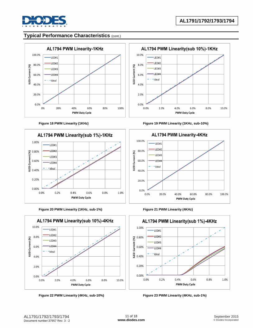
Typical Performance Characteristics (cont.)
Figure 18 PWM Linearity (1KHz) Figure 19 PWM Linearity (1KHz, sub-10%)
Figure 20 PWM Linearity (1KHz, sub-1%) Figure 21 PWM Linearity (4KHz)
Figure 22 PWM Linearity (4KHz, sub-10%) Figure 23 PWM Linearity (4KHz, sub-1%)
AL1791/1792/1793/1794 Document number:37957 Rev. 3 - 2
12 of 18 www.diodes.com
September 2015 © Diodes Incorporated
AD
VA
NC
ED
IN
FO
RM
AT
IO
AL1791/1792/1793/1794
Typical Performance Characteristics (cont.)
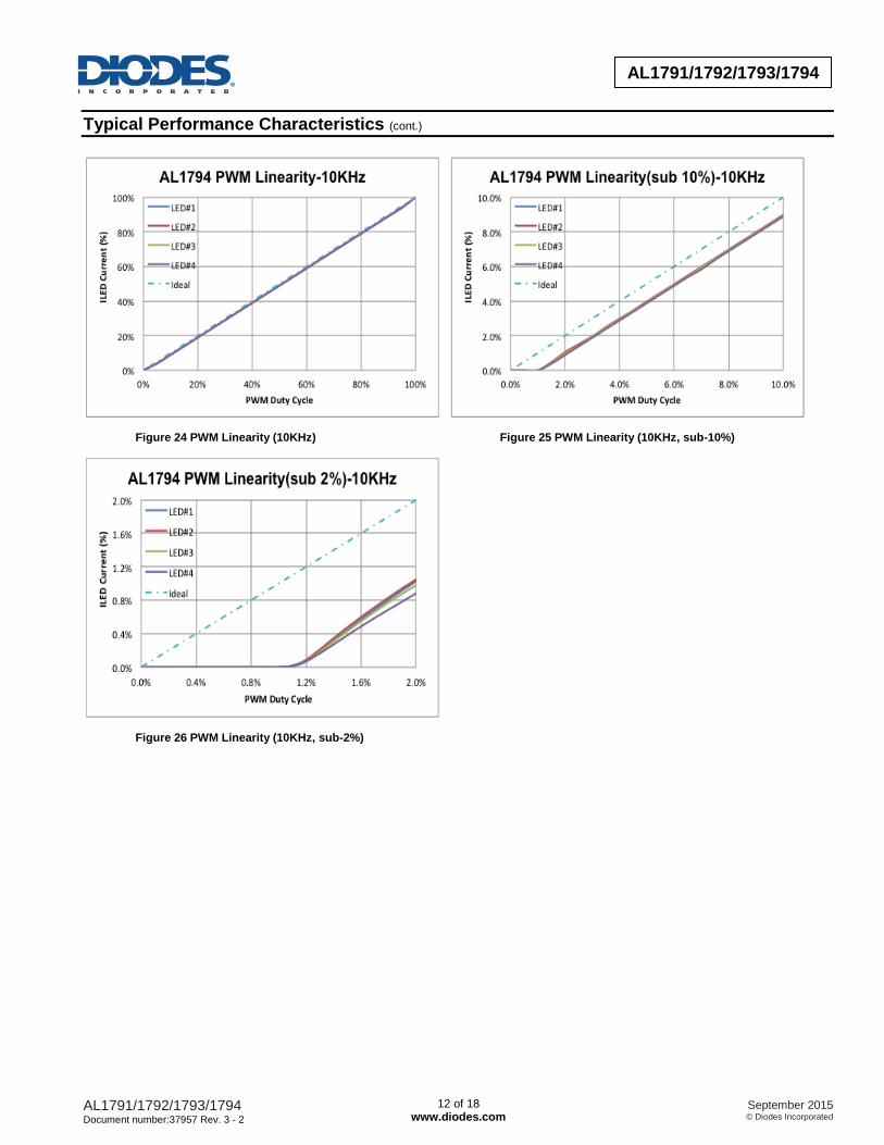
Figure 24 PWM Linearity (10KHz) Figure 25 PWM Linearity (10KHz, sub-10%)
Figure 26 PWM Linearity (10KHz, sub-2%)
AL1791/1792/1793/1794 Document number:37957 Rev. 3 - 2
13 of 18 www.diodes.com
September 2015 © Diodes Incorporated
AD
VA
NC
ED
IN
FO
RM
AT
IO
AL1791/1792/1793/1794
Application Information
Examples of Smart Light Bulb and LED Panel Light System Configurations
Emerging smart LED light bulbs, including Tunable White and Tunable Color products used in either wired or wireless control applications,
address human needs for energy saving, light quality scene setting and entertainment light management. A typical block diagram of a smart light
bulb consists of four major functional blocks: AC to DC Power Conversion, Wireless/Color Management MCU, an LED driver and an emitter
module. The AL179X family fits well with emerging Smart Connected Light bulbs illustrated as below:
1-Channel Dimmable White (Figure 2) Brightness adjustment with Fixed Correlated Color Temperature (CCT) White
2-Channel Tunable White (Figure 3) CCT Tuning with range from 2,700K to 6,500K
3-Channel Tunable Color (Figure 4) Color Mixing for CCT White Generation and Tunable RGB
4-Channel White with Tunable Color (Figure 5) Main White Light with Tunable RGB
For wireless-enabled Smart Connected LED Panel Lights, Troffers, and Ceiling Lights, AL1791/2 can be used to drive emitter string(s) for either 1-
channel Dimmable White or 2-channel Tunable White applications as shown in Figure 2 and Figure 3.
Interface with AC to DC Power Conversion and AL179x
The AC to DC Power Conversion provides necessary output constant voltages (CVs) to power the MCU, and the LED Driver blocks of the entire
smart light bulbs. Typical applications for smart light bulbs might require 3.3V for MCU and 12/24V for LED emitter strings of mainstream smart
light bulbs. Anodes of top LED emitter strings are connected to a 12/24V power supply, and cathodes of bottom LED emitter strings are connected
to LEDx pins of AL179x.
Interface with Wireless/Color Management MCU and AL179x
The main physical interfaces between MCU and AL179x include EN, PWMx pins, and FAULTB. MCU activates the EN (asserted high) to turn on
AL179x in active state for normal LED lighting operation. When EN pin is asserted low, the entire AL1794 enters into shutdown state with
minimum power consumption. For typical light dimming or mixing operations, MCU generates proper PWM signal output through PWMx pins. In
case of any general fault occurring in AL179x, FAULTB pin is asserted LOW to interrupt MCU for proper actions.
LED Driver Design Topology and Implementation
AL179x-powered LED Driver/Emitter block adopts a multi-channel LED driver structure with either analog or PWM dimming control for each
channel. The parallel LED driver channel structure covers mainstream applications for Smart Connected Lighting products. Given the maximum
allowable input voltage of 30V, AL179x can support an LED string up to 8 emitters of W, B, G (assuming LED Emitter Forward Voltage Drop,
VF~3.1V) or 10 emitters of R (assuming VF ~2.2V) in series.
For 1-channel Dimmable White (Figure 2), the Reference Current (IREF) of AL179x is set by an external resistor RSET. In the case using 10KΩ as
RSET, Channel 1 of AL1791 will be driving emitter string(s) with a total constant current of 600mA.
As an example of a 2-channel Tunable White light bulb design (Figure 3), an AL1792 drives two emitter strings, namely, CCTcold (6,500K) and
CCTwarm (2,700K). Using an RSET of 8.5KΩ, the maximum current for Channel 1 and Channel 2 will be 353mA if each PWM signal is turned on.
The associated MCU could generate suitable PWM patterns to meet the required CCT tuning to target light output.
In the case of 3-channel Tunable Color light bulb, AL1794 (Figure 4) drives three separate channels attached to different color emitters (Green -
Channel 1, Red - Channel 2, and Blue - Channel 3). The additional channel (Channel 4 in the example) could be connected to Channel 1 to
enhance green light output. Any given CIE coordinates within the Color Triangle formed by CIE coordinates of three color emitters can be
generated by proper PWM signal pattern generated by the MCU. Therefore, CCT white light tuning tracing the CIE Planckian Locus could be
achieved.
In the case of 4-channel White RGB light bulb (Figure 5), combination of AL1791 and AL1793 ICs are used to drive four separate emitter strings,
White, Green, Red, and Blue emitters. This system configuration provides more flexibility in channel current settings and higher white light output.
AL1791/1792/1793/1794 Document number:37957 Rev. 3 - 2
14 of 18 www.diodes.com
September 2015 © Diodes Incorporated
AD
VA
NC
ED
IN
FO
RM
AT
IO
AL1791/1792/1793/1794
Application Information (continued)
Support Higher Current
While the recommended maximum ILED1 is at 500mA for AL1792/1793/1794, by setting RSET at 6KΩ, the system design can drive an LED string
with higher current by connecting the cathodes of the LED emitter string to two or more LED channel outputs (LEDx) and associated PWM pins
(PWMx) with the same PWM signal from the MCU. The result current through the LED emitter string is the sum of each current through the
individual channels. For example, one can achieve a total of 1.5A by connecting the only one LED emitter string to all four LED channel outputs
AL1793 or AL1794 for a fixed CCT lighting application.
Similarly, it is also possible to further increase the current for a specific channel by connecting two or more AL179x IC chips in parallel and drive all
associated PWM pins with a common PWM signal.
Dimming Performance
For PWM-dimmed light sources, there are two important performance aspects to pay attention to, namely, PWM frequency and deep dimming
performance. While human eyes cannot discern any flickering caused by PWM-dimming light sources over 200Hz, electronic devices such as
cameras for smartphones can detect flickering (referred to as e-Flicker) caused by certain much higher PWM-dimmed light sources. Generally
speaking, the higher the PWM dimming signals applied to the light source, the less e-Flicker is detected by electronic components. The Smart
Light bulb design could leverage the fast response time enabled by AL179x by applying PWM signals over 4KHz, which has been experimented to
be free of e-Flicker.
Measured light is linearly proportional to the measured current and PWM duty cycle. The perceived light by human eyes has a non-linear
relationship with measured light. Human eyes are also found to be more sensitive to low light situations. For example, 10% measured light is
perceived to be 32% of the original full light. 5% measured light is perceived to be 22% of the original full light. 1% measured light is perceived to
be 10% of the original full light. Therefore, deeper dimming such as less-than 0.4% at 4KHz PWM frequency can save significant energy as well
as to provide adequate visible light output.
Special System Design Considerations
Three key Smart Light Bulb system design issues need to be carefully planned for system efficiency consideration. Any headroom voltage (over
total voltage drops for all LED emitters in a string) in each channel will result in additional power consumption for AL179x, which needs to be
dissipated by AL179x. System designers are advised to carefully plan for forward-voltage-matched LED strings with Constant Voltage (CV)
regulators to ensure that AL179x can properly dissipate heat for normal operations.
(1) VF Matching for Emitter Strings: It is crucial to match the total forward voltage drop (VF) of each LED string attached to a CV for optimal
system efficiency.
(2) Multiple CVs to Match Emitter Module Design: The AC to DC Power Conversion block may need to support multiple CV outputs to power
all emitter strings in a Smart Light Bulb design.
(3) Overall Thermal Management: Though there are various protection mechanisms built into AL179x, it is good practice to check the maximum
dimming patterns to avoid Thermal Shutdown (when Al179x junction temperature exceeds +160°C). Thermal resistivity θja (Junction-to-
Ambient) of AL179x is +55°C/Watt. AL179x has to absorb any additional voltage headroom provided by the voltage input to the emitter strings.
Therefore, thermal management of AL179x must follow the following guidelines:
PDmax (Maximum Power Dissipation of AL179x) = (160ºC Junction Shutdown Temperature - Ambient Temperature, e.g. 85°C) /
55°C/W = 1.364Watts
PAmax (Power to be Absorbed by AL179x) = Σ(VLEDx * Current through the emitter string * Associated PWM Dimming Duty
Cycle) for all channels
Thermal Management Guideline PAmax < Pdmax
AL1791/1792/1793/1794 Document number:37957 Rev. 3 - 2
15 of 18 www.diodes.com
September 2015 © Diodes Incorporated
AD
VA
NC
ED
IN
FO
RM
AT
IO
AL1791/1792/1793/1794
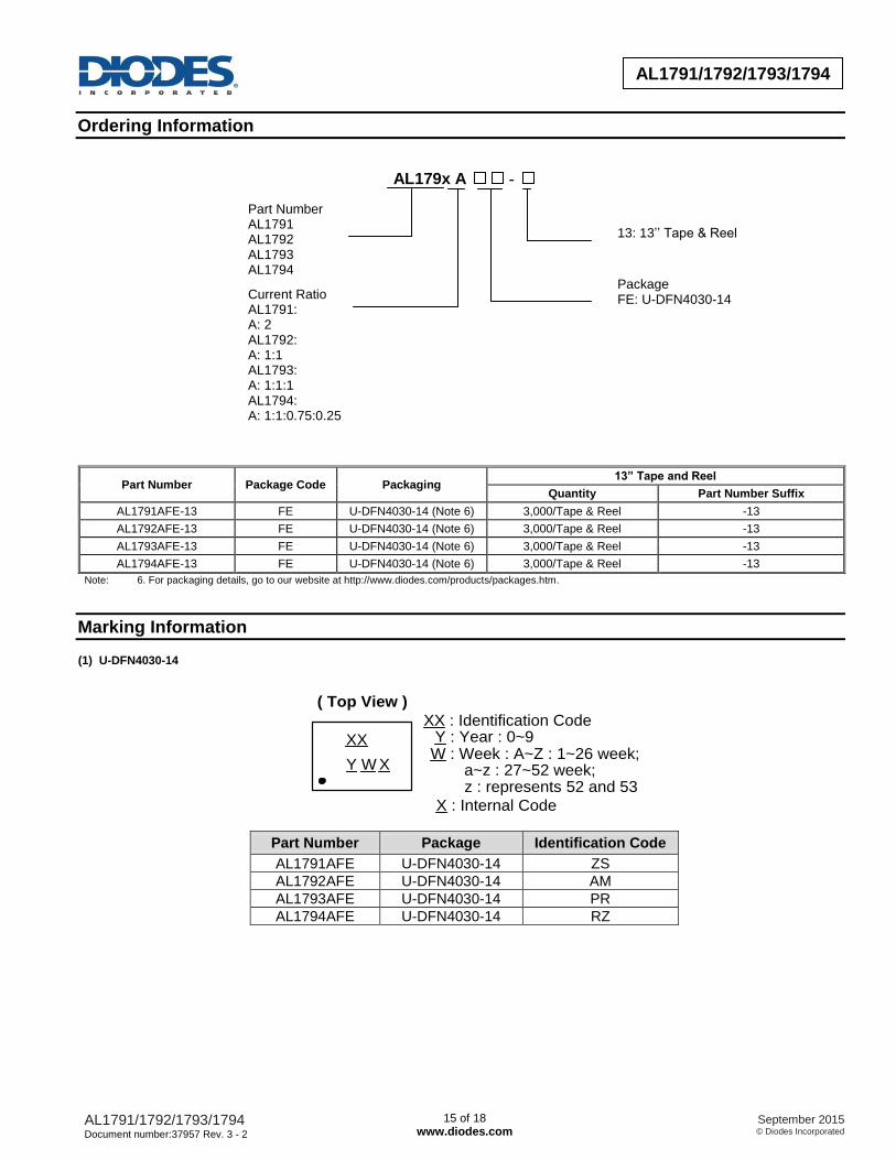
Ordering Information
AL179x A -
Part Number Package Code Packaging 13” Tape and Reel
Quantity Part Number Suffix
AL1791AFE-13 FE U-DFN4030-14 (Note 6) 3,000/Tape & Reel -13
AL1792AFE-13 FE U-DFN4030-14 (Note 6) 3,000/Tape & Reel -13
AL1793AFE-13 FE U-DFN4030-14 (Note 6) 3,000/Tape & Reel -13
AL1794AFE-13 FE U-DFN4030-14 (Note 6) 3,000/Tape & Reel -13
Note: 6. For packaging details, go to our website at http://www.diodes.com/products/packages.htm.
Marking Information (1) U-DFN4030-14
Part Number Package Identification Code
AL1791AFE U-DFN4030-14 ZS
AL1792AFE U-DFN4030-14 AM
AL1793AFE U-DFN4030-14 PR
AL1794AFE U-DFN4030-14 RZ
Y : Year : 0~9
W : Week : A~Z : 1~26 week;
( Top View )
X : Internal Code
Y W X
XX XX : Identification Code
z : represents 52 and 53 a~z : 27~52 week;
13: 13’’ Tape & Reel
Package FE: U-DFN4030-14
Current Ratio AL1791: A: 2 AL1792: A: 1:1 AL1793: A: 1:1:1 AL1794: A: 1:1:0.75:0.25
Part Number AL1791 AL1792 AL1793 AL1794
AL1791/1792/1793/1794 Document number:37957 Rev. 3 - 2
16 of 18 www.diodes.com
September 2015 © Diodes Incorporated
AD
VA
NC
ED
IN
FO
RM
AT
IO
AL1791/1792/1793/1794
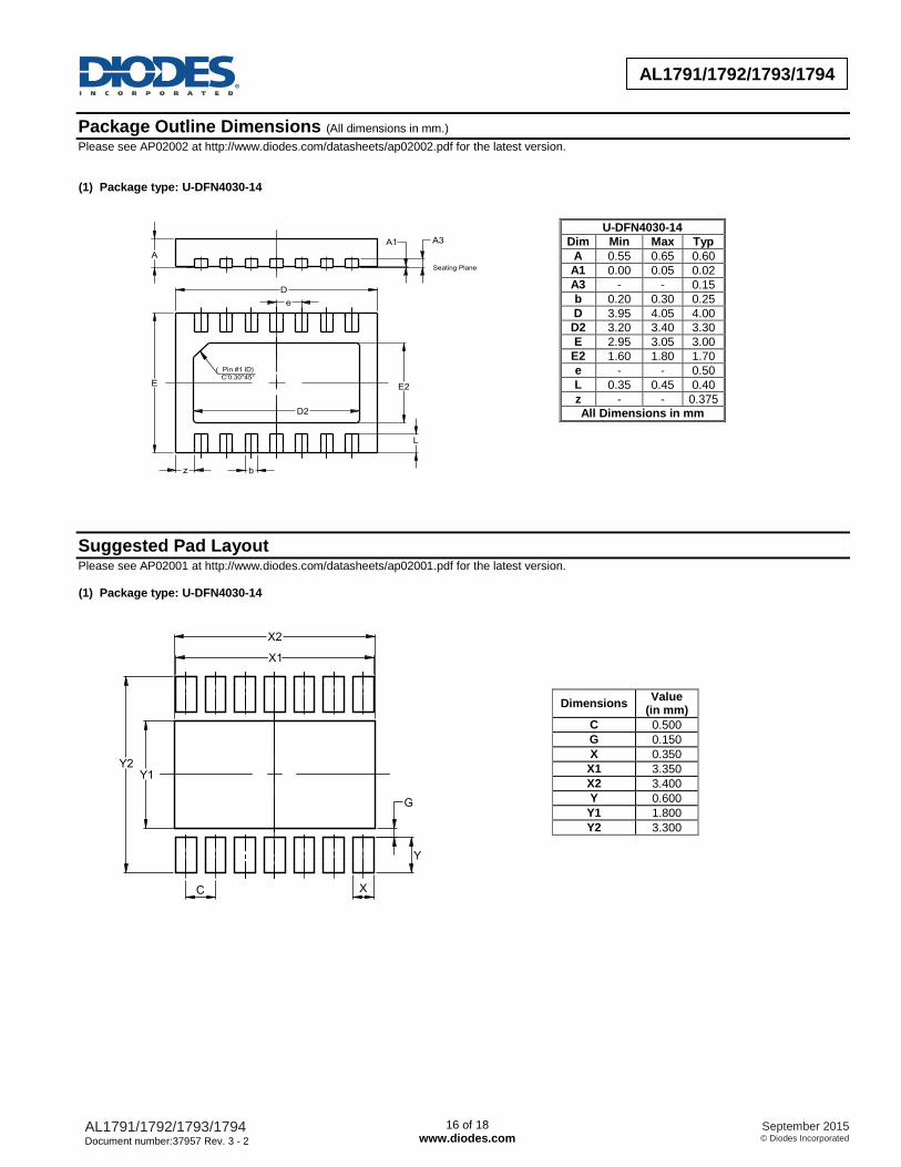
Package Outline Dimensions (All dimensions in mm.)
Please see AP02002 at http://www.diodes.com/datasheets/ap02002.pdf for the latest version. (1) Package type: U-DFN4030-14
Suggested Pad Layout Please see AP02001 at http://www.diodes.com/datasheets/ap02001.pdf for the latest version. (1) Package type: U-DFN4030-14
A
A3
Seating Plane
D
E
b
E2
(Pin #1 ID)
L
D2
e
z
A1
C'0.30*45°
X1
X2
Y2Y1
X
Y
C
G
U-DFN4030-14
Dim Min Max Typ
A 0.55 0.65 0.60
A1 0.00 0.05 0.02
A3 - - 0.15
b 0.20 0.30 0.25
D 3.95 4.05 4.00
D2 3.20 3.40 3.30
E 2.95 3.05 3.00
E2 1.60 1.80 1.70
e - - 0.50
L 0.35 0.45 0.40
z - - 0.375
All Dimensions in mm
Dimensions Value
(in mm)
C 0.500
G 0.150
X 0.350
X1 3.350
X2 3.400
Y 0.600
Y1 1.800
Y2 3.300
AL1791/1792/1793/1794 Document number:37957 Rev. 3 - 2
17 of 18 www.diodes.com
September 2015 © Diodes Incorporated
AD
VA
NC
ED
IN
FO
RM
AT
IO
AL1791/1792/1793/1794
Taping Orientation
(1) Package type: U-DFN4030-14 (Note 7)
Note: 7. The taping orientation of the other package type can be found on our website at http://www.diodes.com/datasheets/ap02007.pdf.
AL1791/1792/1793/1794 Document number:37957 Rev. 3 - 2
18 of 18 www.diodes.com
September 2015 © Diodes Incorporated
AD
VA
NC
ED
IN
FO
RM
AT
IO
AL1791/1792/1793/1794
IMPORTANT NOTICE DIODES INCORPORATED MAKES NO WARRANTY OF ANY KIND, EXPRESS OR IMPLIED, WITH REGARDS TO THIS DOCUMENT, INCLUDING, BUT NOT LIMITED TO, THE IMPLIED WARRANTIES OF MERCHANTABILITY AND FITNESS FOR A PARTICULAR PURPOSE (AND THEIR EQUIVALENTS UNDER THE LAWS OF ANY JURISDICTION). Diodes Incorporated and its subsidiaries reserve the right to make modifications, enhancements, improvements, corrections or other changes without further notice to this document and any product described herein. Diodes Incorporated does not assume any liability arising out of the application or use of this document or any product described herein; neither does Diodes Incorporated convey any license under its patent or trademark rights, nor the rights of others. Any Customer or user of this document or products described herein in such applications shall assume all risks of such use and will agree to hold Diodes Incorporated and all the companies whose products are represented on Diodes Incorporated website, harmless against all damages. Diodes Incorporated does not warrant or accept any liability whatsoever in respect of any products purchased through unauthorized sales channel. Should Customers purchase or use Diodes Incorporated products for any unintended or unauthorized application, Customers shall indemnify and hold Diodes Incorporated and its representatives harmless against all claims, damages, expenses, and attorney fees arising out of, directly or indirectly, any claim of personal injury or death associated with such unintended or unauthorized application. Products described herein may be covered by one or more United States, international or foreign patents pending. Product names and markings noted herein may also be covered by one or more United States, international or foreign trademarks. This document is written in English but may be translated into multiple languages for reference. Only the English version of this document is the final and determinative format released by Diodes Incorporated.
LIFE SUPPORT Diodes Incorporated products are specifically not authorized for use as critical components in life support devices or systems without the express written approval of the Chief Executive Officer of Diodes Incorporated. As used herein: A. Life support devices or systems are devices or systems which: 1. are intended to implant into the body, or
2. support or sustain life and whose failure to perform when properly used in accordance with instructions for use provided in the labeling can be reasonably expected to result in significant injury to the user.
B. A critical component is any component in a life support device or system whose failure to perform can be reasonably expected to cause the failure of the life support device or to affect its safety or effectiveness. Customers represent that they have all necessary expertise in the safety and regulatory ramifications of their life support devices or systems, and acknowledge and agree that they are solely responsible for all legal, regulatory and safety-related requirements concerning their products and any use of Diodes Incorporated products in such safety-critical, life support devices or systems, notwithstanding any devices- or systems-related information or support that may be provided by Diodes Incorporated. Further, Customers must fully indemnify Diodes Incorporated and its representatives against any damages arising out of the use of Diodes Incorporated products in such safety-critical, life support devices or systems. Copyright © 2015, Diodes Incorporated www.diodes.com