pzt stack etch for mems devices in a capacitively coupled ... · pzt stack etch for mems devices in...
TRANSCRIPT
PZT stack etch for MEMS devices in a capacitively coupled highdensity plasma reactor
Paul Werbaneth*, John Almerico, Les Jerde, Steve MarksTegal Corporation
ABSTRACT
Ferroelectric thin films like lead zirconate titanate (PZT) are used to form several different families of MEMS devices.Moving mirrors for optical switching applications utilize the piezoelectric properties of PZT; varactors depend on itsdielectric nonlinearity. The oxidizing environment during PZT deposition means that some material capable of resistingoxidation, like platinum, must be used as the metal electrode in any metal-ferroelectric-metal (MFM) stack. Ion millinghas been used in laboratory applications for patterning MFM stacks. However, ion milling removal rates are low(~400Å/min), the throughputs are low, and the etched materials tend to redeposit along the edge of the etch mask,creating veils, or fences, after the etch mask is removed. These residues can lead to yield-limiting defects in finisheddevices. We report here on MFM stack etch results from a capacitively coupled high density plasma etch reactor. Usingphotoresist masks, we have demonstrated platinum and PZT etch rates greater than 1000Å/min at moderate (80ºC) wafertemperatures. Good etch profiles with no post-etch residue are produced for MFM stacks like those used for a MEMS-based Atomic Force Microscopy application, for example, which employs a bottom platinum layer 1500Å thick, 2800Åof PZT, and a platinum top electrode of 1500Å.
Keywords: PZT etch, platinum etch, MFM stack etch, plasma etch
1. INTRODUCTION
Plasma etch is employed in modern microelectronic fabrication processes to faithfully reproduce masking image featuresinto the permanent layers of a device or circuit. The benefits of plasma etch include the ability to etch sub-micronstructures without changing critical dimensions while maintaining good selectivity to the masking and underlyingmaterials in the sustained production environment of a commercial wafer fabrication facility. Manufacturing processesfor MEMS, and MOEMS, are similar to those processes used by the large integrated device makers for high-volumeCMOS products: the basic sequence of thin film deposition, photolithography, and etch is repeated many times to makea finished MEMS device. However, the many novel structures and materials employed in MEMS fabrication cause it todiverge in several important ways from the family of standard silicon processing modules.
1.1. Uses of MFM structures for MEMS applicationsPZT is a useful material for many different MEMS applications, most prominently those applications requiring physicalmotion, like moving mirrors in optical switch fabrics (PZT is a piezoelectric material), and those for which the ability toadjust device capacitance, for example acoustic filters for RF communication applications, is important. The oxidizingenvironment found during the deposition and annealing of PZT films means that some electrode material capable ofresisting oxidation (platinum) or capable of forming an electrically conductive oxide (iridium) must be used with PZT,creating what is called an MFM (metal – ferroelectric – metal) stack. This is very different from the capacitor structuresand metalization schemes found in CMOS processing, where the dielectric materials are typically silicon dioxide orsilicon oxynitride, and the electrode materials silicon, polysilicon, or aluminum and aluminum alloys.
* [email protected]; phone 1.707.765.5608; fax 1.707.773.3015; Tegal Corporation, 2201 S. McDowell Blvd.,Petaluma, CA, USA 94954
1.2. Patterning MFM structuresPatterning MFM structures is inherently challenging. Due to the nonvolatility of the etch products produced duringMFM stack etch, it is difficult to successfully integrate MFM stacks into microelectronic devices1,2.
Some candidates for etching these difficult materials are wet etch, chemical-plasma etch, reactive ion etch, and ionmilling. Wet etches suffer from feature size limitations; chemical-plasma etch offers only limited etch rates.
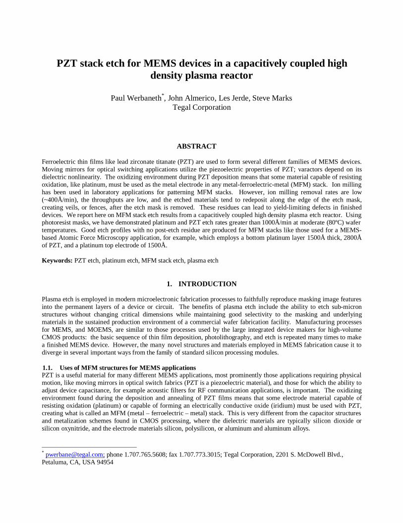
1.3. Ion milling limitationsIon Milling, or Ion Beam Etching, has been a versatile tool in laboratory applications for patterning almost any knownmaterial. The physical action of the ion beam can be made to be sufficiently energetic to remove atoms from solid thinfilm surfaces under temperature and pressure conditions where the vapor pressure of the material(s) to be removed isnegligibly small. Ion milling lends itself perfectly to laboratory demonstrations of MFM capacitor formation, where theproblem of patterning the noble metal electrodes and the heavy metals in the ferroelectric films, at the feasibility stage ofdevice fabrication, does not warrant extensive exploration of other patterning techniques. Researchers have notedseveral drawbacks to ion milling: for example, when ion milling is used to pattern platinum, the removal rate ofplatinum is low (~400Å/min); the overall tool throughput, as a result of the combination of low etch rates and the needfor long overetches, is poor; and the tendency of the etched material to redeposit on the side of the etch mask, andremain, causes the formation of fearsome veils, or fences, after the etch mask has been removed. These veils can lead toyield-limiting electrical defects in finished devices. Figure 1 is an example of the kind of veil observed post-etch ( andafter photoresist mask removal) for a dry-etched platinum feature.
Figure 1Veil formed after dry etch of platinum
This shortcoming has motivated us to develop alternative dry patterning processes for MFM stacks.
2. EXPERIMENTAL APPARATUS
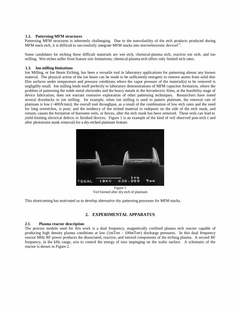
2.1. Plasma reactor descriptionThe process module used for this work is a dual frequency, magnetically confined plasma etch reactor capable ofproducing high density plasma conditions at low (1mTorr - 100mTorr) discharge pressures. In this dual frequencyreactor MHz RF power produces the dissociated, reactive, and ionized components of the etching plasma. A second RFfrequency, in the kHz range, acts to control the energy of ions impinging on the wafer surface. A schematic of thereactor is shown in Figure 2.
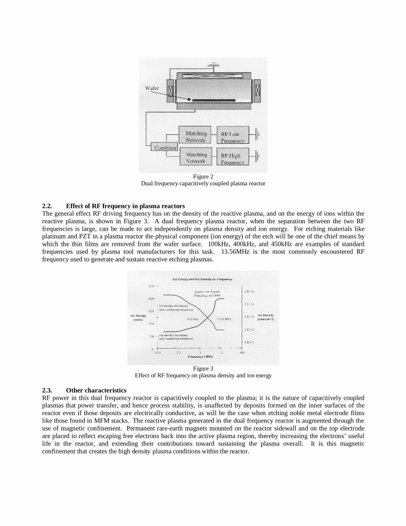
Figure 2Dual frequency capacitively coupled plasma reactor
2.2. Effect of RF frequency in plasma reactorsThe general effect RF driving frequency has on the density of the reactive plasma, and on the energy of ions within thereactive plasma, is shown in Figure 3. A dual frequency plasma reactor, when the separation between the two RFfrequencies is large, can be made to act independently on plasma density and ion energy. For etching materials likeplatinum and PZT in a plasma reactor the physical component (ion energy) of the etch will be one of the chief means bywhich the thin films are removed from the wafer surface. 100kHz, 400kHz, and 450kHz are examples of standardfrequencies used by plasma tool manufacturers for this task. 13.56MHz is the most commonly encountered RFfrequency used to generate and sustain reactive etching plasmas.
Figure 3Effect of RF frequency on plasma density and ion energy
2.3. Other characteristicsRF power in this dual frequency reactor is capacitively coupled to the plasma; it is the nature of capacitively coupledplasmas that power transfer, and hence process stability, is unaffected by deposits formed on the inner surfaces of thereactor even if those deposits are electrically conductive, as will be the case when etching noble metal electrode filmslike those found in MFM stacks. The reactive plasma generated in the dual frequency reactor is augmented through theuse of magnetic confinement. Permanent rare-earth magnets mounted on the reactor sidewall and on the top electrodeare placed to reflect escaping free electrons back into the active plasma region, thereby increasing the electrons’ usefullife in the reactor, and extending their contributions toward sustaining the plasma overall. It is this magneticconfinement that creates the high density plasma conditions within the reactor.
3. STRATEGY FOR PLASMA ETCH OPTIMIZATION OF MFM STACKS
The basic concept of plasma etching is very straightforward. A glow discharge is used to generate chemically reactive species
(atoms, radicals, ions) from a relatively inert molecular gas. The etching gas is chosen so as to produce species which react
chemically with the material to be etched to form a reaction product which is volatile (at room temperature preferably). The etch
product then spontaneously desorbs from the etched material into the gas phase where it is removed by the vacuum pumping
system. The key requirement is the volatility of the etch product3.
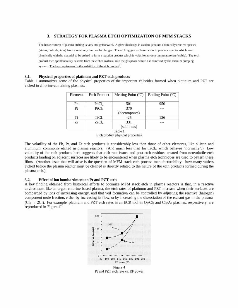
3.1. Physical properties of platinum and PZT etch productsTable 1 summarizes some of the physical properties of the important chlorides formed when platinum and PZT areetched in chlorine-containing plasmas.
Element Etch Product Melting Point (ºC) Boiling Point (ºC)
Pb PbCl2 501 950Pt PtCl4 370
(decomposes)---
Ti TiCl4 -25 136Zr ZrCl4 331
(sublimes)---
Table 1Etch product physical properties
The volatility of the Pb, Pt, and Zr etch products is considerably less than those of other elements, like silicon andaluminum, commonly etched in plasma reactors. (And much less than for TiCl4, which behaves “normally”.) Lowvolatility of the etch products here suggests that etch rate issues and post-etch residues created from nonvolatile etchproducts landing on adjacent surfaces are likely to be encountered when plasma etch techniques are used to pattern thesefilms. (Another issue that will arise is the question of MFM stack etch process manufacturability: how many wafersetched before the plasma reactor must be cleaned is directly related to the nature of the etch products formed during theplasma etch.)
3.2. Effect of ion bombardment on Pt and PZT etchA key finding obtained from historical efforts to optimize MFM stack etch in plasma reactors is that, in a reactiveenvironment like an argon-chlorine-based plasma, the etch rates of platinum and PZT increase when their surfaces arebombarded by ions of increasing energy, and that veil formation can be controlled by adjusting the reactive (halogen)component mole fraction, either by increasing its flow, or by increasing the dissociation of the etchant gas in the plasma(Cl2 → 2Cl). For example, platinum and PZT etch rates in an ECR tool in O2/Cl2 and Cl2/Ar plasmas, respectively, arereproduced in Figure 44.
Figure 4Pt and PZT etch rate vs. RF power
4. MFM STACK ETCH DATA
Etch rates and post-etch veil formation for photoresist masked platinum films were characterized in the dual frequencycapacitively coupled plasma reactor described in Section 2. This characterization was performed using Design OfExperiment techniques. These experimental methods are useful in that they reveal process trends and processinteractions for multi-variable systems. The principle process variables, or experimental factors, in a plasma etch reactorare pressure, temperature, type of reactant used, reactant flows, reactant fraction (in multi-reactant chemistries), plasmadensity, and ion bombardment energy and flux at the wafer surface.
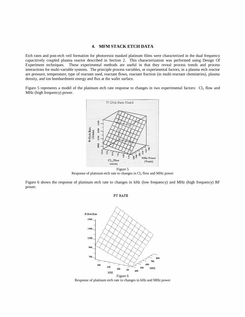
Figure 5 represents a model of the platinum etch rate response to changes in two experimental factors: Cl2 flow andMHz (high frequency) power.
Figure 5Response of platinum etch rate to changes in Cl2 flow and MHz power
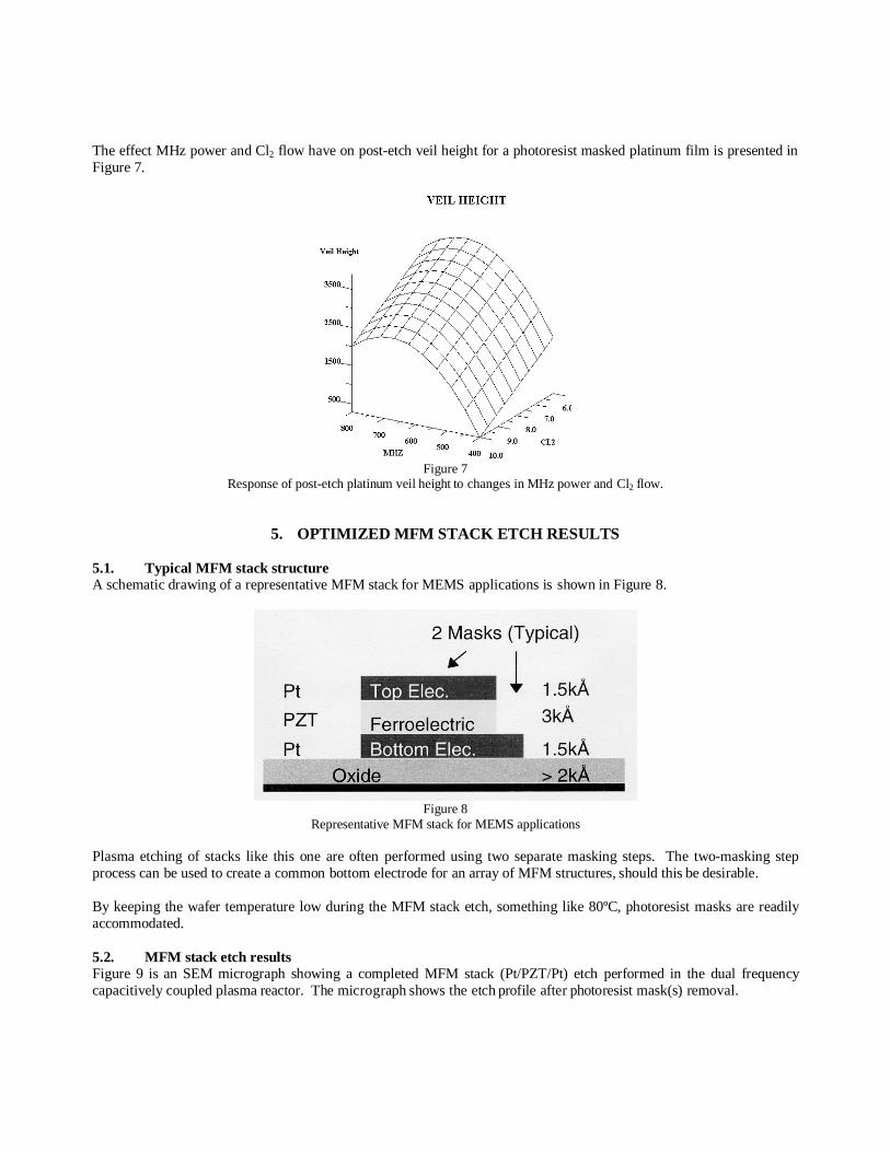
Figure 6 shows the response of platinum etch rate to changes in kHz (low frequency) and MHz (high frequency) RFpower.
Figure 6Response of platinum etch rate to changes in kHz and MHz power
The effect MHz power and Cl2 flow have on post-etch veil height for a photoresist masked platinum film is presented inFigure 7.
Figure 7Response of post-etch platinum veil height to changes in MHz power and Cl2 flow.
5. OPTIMIZED MFM STACK ETCH RESULTS
5.1. Typical MFM stack structureA schematic drawing of a representative MFM stack for MEMS applications is shown in Figure 8.
Figure 8Representative MFM stack for MEMS applications
Plasma etching of stacks like this one are often performed using two separate masking steps. The two-masking stepprocess can be used to create a common bottom electrode for an array of MFM structures, should this be desirable.
By keeping the wafer temperature low during the MFM stack etch, something like 80ºC, photoresist masks are readilyaccommodated.
5.2. MFM stack etch resultsFigure 9 is an SEM micrograph showing a completed MFM stack (Pt/PZT/Pt) etch performed in the dual frequencycapacitively coupled plasma reactor. The micrograph shows the etch profile after photoresist mask(s) removal.
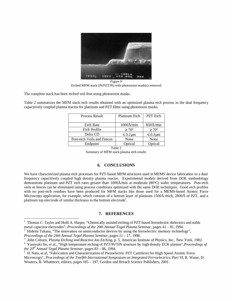
Figure 9Etched MFM stack (Pt/PZT/Pt) with photoresist mask(s) removed
The complete stack has been etched veil-free using photoresist masks.
Table 2 summarizes the MFM stack etch results obtained with an optimized plasma etch process in the dual frequencycapacitively coupled plasma reactor for platinum and PZT films using photoresist masks.
Process Result Platinum Etch PZT Etch
Etch Rate 1000Å/min 850Å/minEtch Profile ≥ 70º ≥ 70º
Delta CD ≤ 0.2µm ≤ 0.3µmPost-etch Veils and Fences None None
Endpoint Optical OpticalTable 2
Summary of MFM stack plasma etch results
6. CONCLUSIONS
We have characterized plasma etch processes for PZT-based MFM structures used in MEMS device fabrication in a dualfrequency capacitively coupled high density plasma reactor. Experimental models derived from DOE methodologydemonstrate platinum and PZT etch rates greater than 1000Å/min at moderate (80ºC) wafer temperatures. Post-etchveils or fences can be eliminated using process conditions optimized with the same DOE techniques. Good etch profileswith no post-etch residues have been produced for MFM stacks like those used for a MEMS-based Atomic ForceMicroscopy application, for example, which consists of a bottom layer of platinum 1500Å thick, 2800Å of PZT, and aplatinum top electrode of similar thickness to the bottom electrode5.
7. REFERENCES 1 Thomas C. Taylor and Holli A. Harper, “Chemically assisted etching of PZT-based ferroelectric dielectrics and noblemetal capacitor electrodes”, Proceedings of the 20th Annual Tegal Plasma Seminar, pages 41 – 81, 1994.2 Hidemi Takasu, “The innovation on semiconductor devices by using the ferroelectric memory technology”,Proceedings of the 24th Annual Tegal Plasma Seminar, pages 11 – 17, 1998.3 John Coburn, Plasma Etching and Reactive Ion Etching, p. 5, American Institute of Physics, Inc., New York, 1982.4 Yasuyuki Ito, et al., “High temperature etching of PZT/Pt/TiN structure by high density ECR plasma”, Proceedings ofthe 20th Annual Tegal Plasma Seminar, pages 83 – 86, 1994.5 H. Nam, et al, "Fabrication and Characterization of Piezoelectric PZT Cantilever for High Speed Atomic ForceMicroscopy", Proceedings of the Twelfth International Symposium on Integrated Ferroelectrics, Part VI, R. Waser, D.Wouters, R. Whatmore, editors, pages 185 – 197, Gordon and Breach Science Publishers, 2001.