quad low-sidedriver ic - embedded adventures · quad low-sidedriver ic check for samples: drv8803...
TRANSCRIPT
DRV8803
www.ti.com SLVSAW5B –JULY 2011–REVISED FEBRUARY 2012
QUAD LOW-SIDE DRIVER ICCheck for Samples: DRV8803
1FEATURES2• 4-Channel Protected Low-Side Driver • 8.2-V to 60-V Operating Supply Voltage Range
– Four NMOS FETs With Overcurrent • Thermally Enhanced Surface Mount PackageProtection
APPLICATIONS– Integrated Inductive Catch Diodes• Relay Drivers– Parallel Interface• Unipolar Stepper Motor Drivers• DW Package: 1.5-A (Single Channel On) /
800-mA (Four Channels On) Maximum Drive • Solenoid DriversCurrent per Channel (at 25°C) • General Low-Side Switch Applications
• PWP Package: 2-A (Single Channel On) /1-A (Four Channels On) Maximum DriveCurrent per Channel (at 25°C, With Proper PCBHeatsinking)
DESCRIPTIONThe DRV8803 provides a 4-channel low side driver with overcurrent protection. It has built-in diodes to clampturn-off transients generated by inductive loads and can be used to drive unipolar stepper motors, DC motors,relays, solenoids, or other loads.
In the SOIC (DW) package, the DRV8803 can supply up to 1.5-A (one channel on) or 800-mA (all channels on)continuous output current per channel, at 25°C. In the HTSSOP (PWP) package, it can supply up to 2-A (onechannel on) or 1-A (four channels on) continuous output current per channel, at 25°C with proper PCBheatsinking.
The device is controlled via a simple parallel interface.
Internal shutdown functions are provided for over current protection, short circuit protection, under voltagelockout and overtemperature and faults are indicated by a fault output pin.
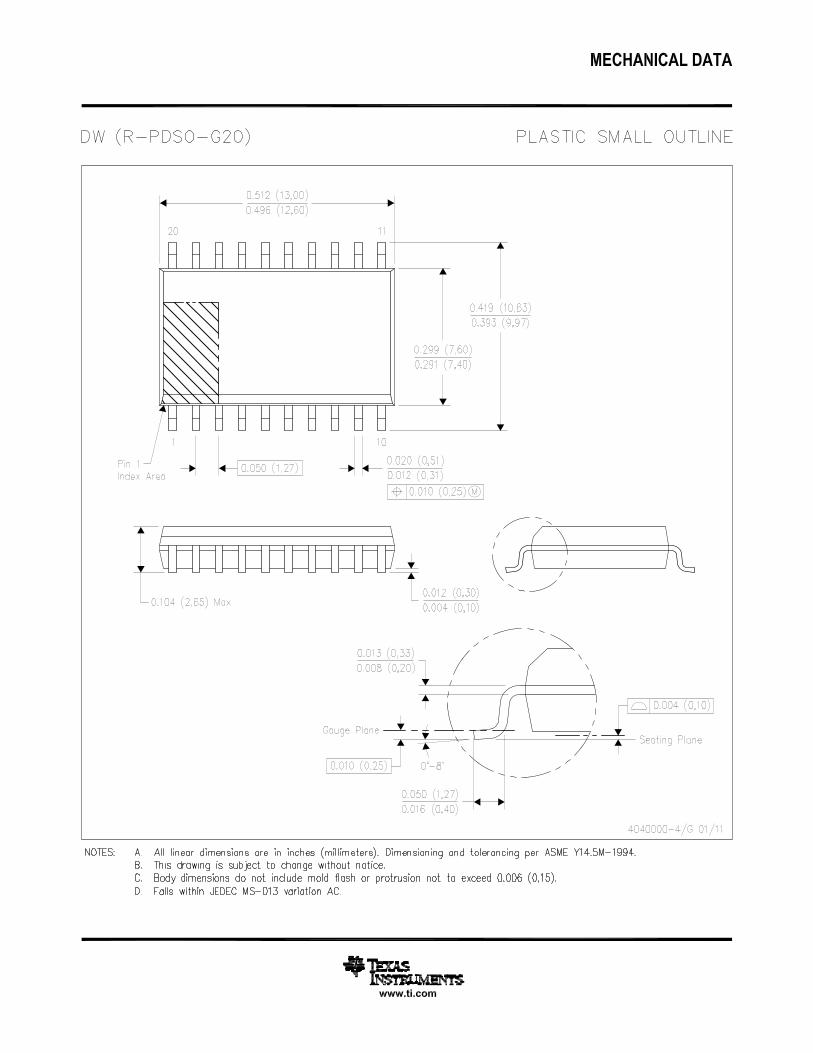
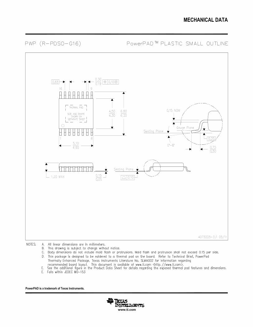
The DRV8803 is available in a 20-pin thermally-enhanced SOIC package and a 16-pin HTSSOP package (Eco-friendly: RoHS & no Sb/Br).
ORDERING INFORMATION (1)
ORDERABLE PART TOP-SIDEPACKAGE (2)NUMBER MARKING
Reel of 2000 DRV8803DWR DRV8803(SOIC) - DW
Tube of 25 DRV8803DW DRV8803
Reel of 2000 DRV8803PWPR DRV8803(HTSSOP) - PWP
Tube of 90 DRV8803PWP DRV8803
(1) For the most current packaging and ordering information, see the Package Option Addendum at the end of this document, or see the TIweb site at www.ti.com.
(2) Package drawings, thermal data, and symbolization are available at www.ti.com/packaging.
1
Please be aware that an important notice concerning availability, standard warranty, and use in critical applications ofTexas Instruments semiconductor products and disclaimers thereto appears at the end of this data sheet.
2PowerPAD is a trademark of texas Instruments.
PRODUCTION DATA information is current as of publication date. Copyright © 2011–2012, Texas Instruments IncorporatedProducts conform to specifications per the terms of the TexasInstruments standard warranty. Production processing does notnecessarily include testing of all parameters.
Thermal
Shut down
OUT1
GND
(multiple pins)
VCLAMP
IN1
IN2
IN3
Internal
Reference
Regs
UVLO
Int. VCC
nFAULT
Control
Logic
IN4
nENBL
VMLS Gate
Drive
OUT2
OUT3
OUT4
OCP
&
Gate
Drive
8.2V – 60V
OCP
&
Gate
Drive
OCP
&
Gate
Drive
OCP
&
Gate
Drive
8.2V – 60V
Optional
Zener
Inductive
Load
Inductive
Load
Inductive
Load
Inductive
Load
RESET
DRV8803
SLVSAW5B –JULY 2011–REVISED FEBRUARY 2012 www.ti.com
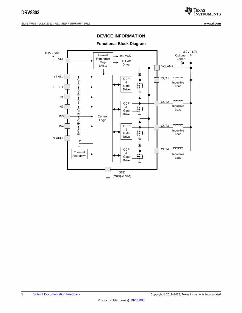
DEVICE INFORMATION
Functional Block Diagram
2 Submit Documentation Feedback Copyright © 2011–2012, Texas Instruments Incorporated
Product Folder Link(s): DRV8803
1
2
3
4
5
6
7
8
9
10
14
13
12
11
15
16
17
18
19
20 nFAULT
NC
IN1
IN2
GND
GND
GND
IN3
IN4
RESET
OUT4
nENBL
GND
OUT3
GND
GND
OUT1
OUT2
VM
VCLAMP
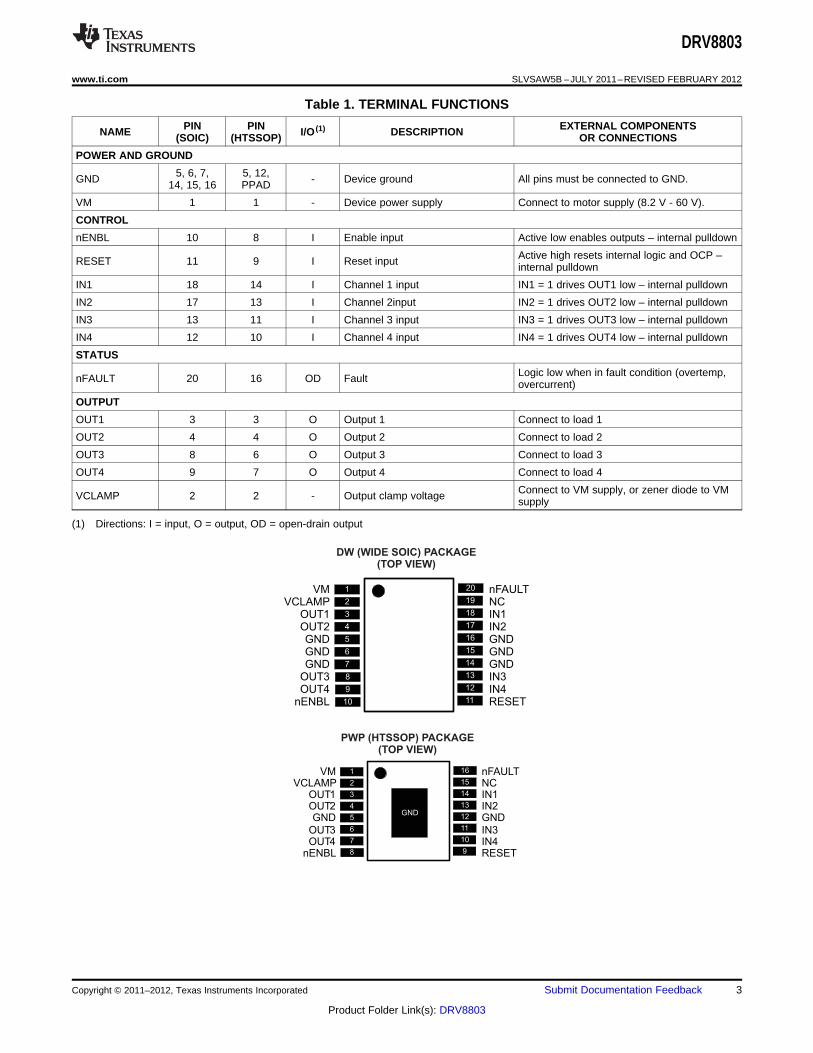
DW (WIDE SOIC) PACKAGE(TOP VIEW)
1
2
3
4
5
6
7
8
10
9
11
12
13
14
15
16 nFAULT
NC
IN1
IN2
GND
IN3
IN4
RESETnENBL
OUT3
OUT4
GND
OUT1
OUT2
VM
VCLAMP
GND
PWP (HTSSOP) PACKAGE(TOP VIEW)
DRV8803
www.ti.com SLVSAW5B –JULY 2011–REVISED FEBRUARY 2012
Table 1. TERMINAL FUNCTIONS
PIN PIN EXTERNAL COMPONENTSNAME I/O (1) DESCRIPTION(SOIC) (HTSSOP) OR CONNECTIONS
POWER AND GROUND
5, 6, 7, 5, 12,GND - Device ground All pins must be connected to GND.14, 15, 16 PPAD
VM 1 1 - Device power supply Connect to motor supply (8.2 V - 60 V).
CONTROL
nENBL 10 8 I Enable input Active low enables outputs – internal pulldown
Active high resets internal logic and OCP –RESET 11 9 I Reset input internal pulldown
IN1 18 14 I Channel 1 input IN1 = 1 drives OUT1 low – internal pulldown
IN2 17 13 I Channel 2input IN2 = 1 drives OUT2 low – internal pulldown
IN3 13 11 I Channel 3 input IN3 = 1 drives OUT3 low – internal pulldown
IN4 12 10 I Channel 4 input IN4 = 1 drives OUT4 low – internal pulldown
STATUS
Logic low when in fault condition (overtemp,nFAULT 20 16 OD Fault overcurrent)
OUTPUT
OUT1 3 3 O Output 1 Connect to load 1
OUT2 4 4 O Output 2 Connect to load 2
OUT3 8 6 O Output 3 Connect to load 3
OUT4 9 7 O Output 4 Connect to load 4
Connect to VM supply, or zener diode to VMVCLAMP 2 2 - Output clamp voltage supply
(1) Directions: I = input, O = output, OD = open-drain output
Copyright © 2011–2012, Texas Instruments Incorporated Submit Documentation Feedback 3
Product Folder Link(s): DRV8803

DRV8803
SLVSAW5B –JULY 2011–REVISED FEBRUARY 2012 www.ti.com
ABSOLUTE MAXIMUM RATINGSover operating free-air temperature range (unless otherwise noted) (1) (2)
VALUE UNIT
VM Power supply voltage range –0.3 to 65 V
VOUTx Output voltage range –0.3 to 65 V
VCLAMP Clamp voltage range –0.3 to 65 V
nFAULT Output current 20 mA
Peak clamp diode current 2 A
DC or RMS clamp diode current 1 A
Digital input pin voltage range –0.5 to 7 V
nFAULT Digital output pin voltage range –0.5 to 7 V
Peak motor drive output current, t < 1 μS Internally limited A
Continuous total power dissipation See Dissipation Ratings table
TJ Operating virtual junction temperature range –40 to 150 °C
Tstg Storage temperature range –60 to 150 °C
(1) Stresses beyond those listed under absolute maximum ratings may cause permanent damage to the device. These are stress ratingsonly, and functional operation of the device at these or any other conditions beyond those indicated under recommended operatingconditions is not implied. Exposure to absolute–maximum–rated conditions for extended periods may affect device reliability.
(2) All voltage values are with respect to network ground terminal.
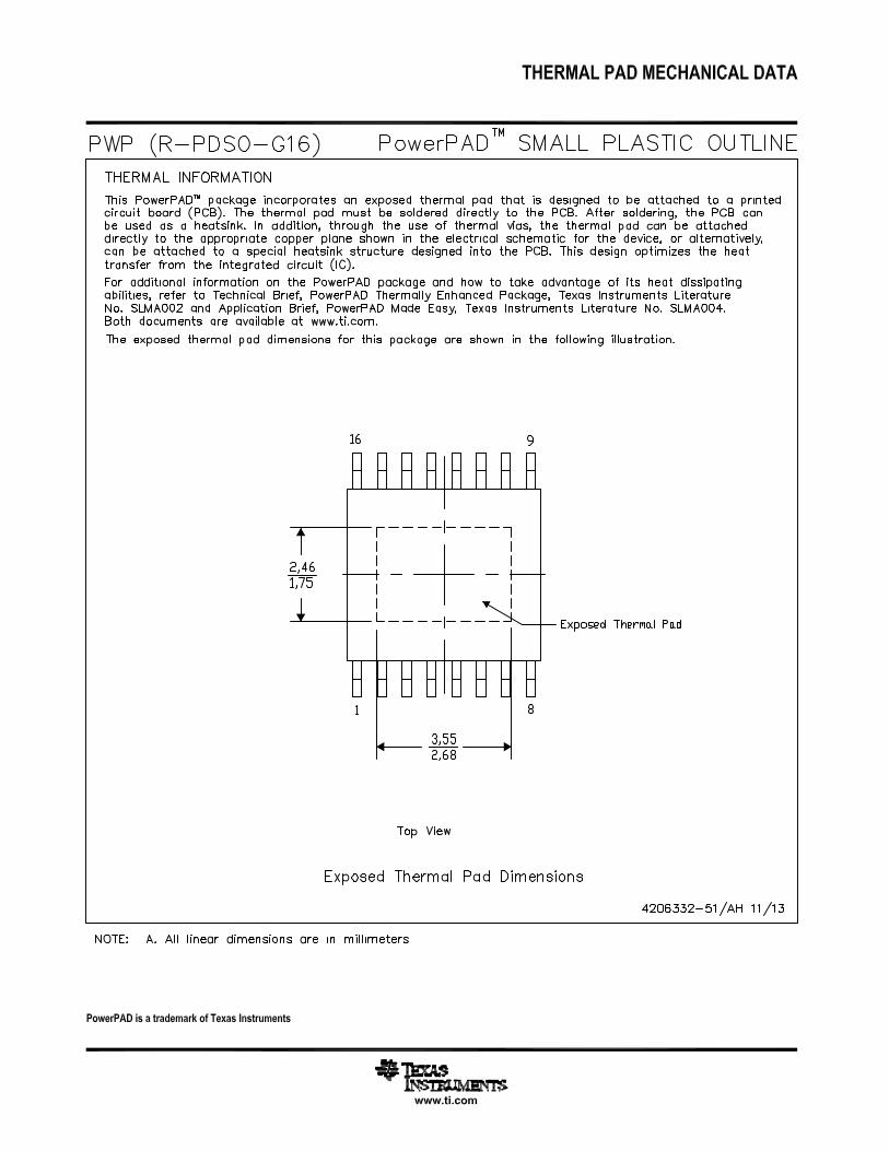
THERMAL INFORMATIONDRV8803 DRV8803
THERMAL METRIC DW PWP UNITS
20 PINS 16 PINS
θJA Junction-to-ambient thermal resistance (1) 67.7 39.6
θJCtop Junction-to-case (top) thermal resistance (2) 32.9 24.6
θJB Junction-to-board thermal resistance (3) 35.4 20.3°C/W
ψJT Junction-to-top characterization parameter (4) 8.2 0.7
ψJB Junction-to-board characterization parameter (5) 34.9 20.1
θJCbot Junction-to-case (bottom) thermal resistance (6) N/A 2.3
(1) The junction-to-ambient thermal resistance under natural convection is obtained in a simulation on a JEDEC-standard, high-K board, asspecified in JESD51-7, in an environment described in JESD51-2a.
(2) The junction-to-case (top) thermal resistance is obtained by simulating a cold plate test on the package top. No specific JEDEC-standard test exists, but a close description can be found in the ANSI SEMI standard G30-88.
(3) The junction-to-board thermal resistance is obtained by simulating in an environment with a ring cold plate fixture to control the PCBtemperature, as described in JESD51-8.
(4) The junction-to-top characterization parameter, ψJT, estimates the junction temperature of a device in a real system and is extractedfrom the simulation data for obtaining θJA, using a procedure described in JESD51-2a (sections 6 and 7).
(5) The junction-to-board characterization parameter, ψJB, estimates the junction temperature of a device in a real system and is extractedfrom the simulation data for obtaining θJA , using a procedure described in JESD51-2a (sections 6 and 7).
(6) The junction-to-case (bottom) thermal resistance is obtained by simulating a cold plate test on the exposed (power) pad. No specificJEDEC standard test exists, but a close description can be found in the ANSI SEMI standard G30-88.
4 Submit Documentation Feedback Copyright © 2011–2012, Texas Instruments Incorporated
Product Folder Link(s): DRV8803
DRV8803
www.ti.com SLVSAW5B –JULY 2011–REVISED FEBRUARY 2012
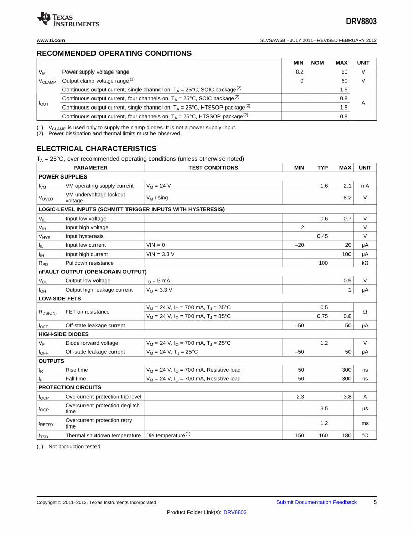
RECOMMENDED OPERATING CONDITIONSMIN NOM MAX UNIT
VM Power supply voltage range 8.2 60 V
VCLAMP Output clamp voltage range (1) 0 60 V
Continuous output current, single channel on, TA = 25°C, SOIC package (2) 1.5
Continuous output current, four channels on, TA = 25°C, SOIC package (2) 0.8IOUT A
Continuous output current, single channel on, TA = 25°C, HTSSOP package (2) 1.5
Continuous output current, four channels on, TA = 25°C, HTSSOP package (2) 0.8
(1) VCLAMP is used only to supply the clamp diodes. It is not a power supply input.(2) Power dissipation and thermal limits must be observed.
ELECTRICAL CHARACTERISTICSTA = 25°C, over recommended operating conditions (unless otherwise noted)
PARAMETER TEST CONDITIONS MIN TYP MAX UNIT
POWER SUPPLIES
IVM VM operating supply current VM = 24 V 1.6 2.1 mA
VM undervoltage lockoutVUVLO VM rising 8.2 Vvoltage
LOGIC-LEVEL INPUTS (SCHMITT TRIGGER INPUTS WITH HYSTERESIS)
VIL Input low voltage 0.6 0.7 V
VIH Input high voltage 2 V
VHYS Input hysteresis 0.45 V
IIL Input low current VIN = 0 –20 20 μA
IIH Input high current VIN = 3.3 V 100 μA
RPD Pulldown resistance 100 kΩnFAULT OUTPUT (OPEN-DRAIN OUTPUT)
VOL Output low voltage IO = 5 mA 0.5 V
IOH Output high leakage current VO = 3.3 V 1 μA
LOW-SIDE FETS
VM = 24 V, IO = 700 mA, TJ = 25°C 0.5RDS(ON) FET on resistance Ω
VM = 24 V, IO = 700 mA, TJ = 85°C 0.75 0.8
IOFF Off-state leakage current –50 50 μA
HIGH-SIDE DIODES
VF Diode forward voltage VM = 24 V, IO = 700 mA, TJ = 25°C 1.2 V
IOFF Off-state leakage current VM = 24 V, TJ = 25°C –50 50 μA
OUTPUTS
tR Rise time VM = 24 V, IO = 700 mA, Resistive load 50 300 ns
tF Fall time VM = 24 V, IO = 700 mA, Resistive load 50 300 ns
PROTECTION CIRCUITS
IOCP Overcurrent protection trip level 2.3 3.8 A
Overcurrent protection deglitchtOCP 3.5 µstime
Overcurrent protection retrytRETRY 1.2 mstime
tTSD Thermal shutdown temperature Die temperature (1) 150 160 180 °C
(1) Not production tested.
Copyright © 2011–2012, Texas Instruments Incorporated Submit Documentation Feedback 5
Product Folder Link(s): DRV8803
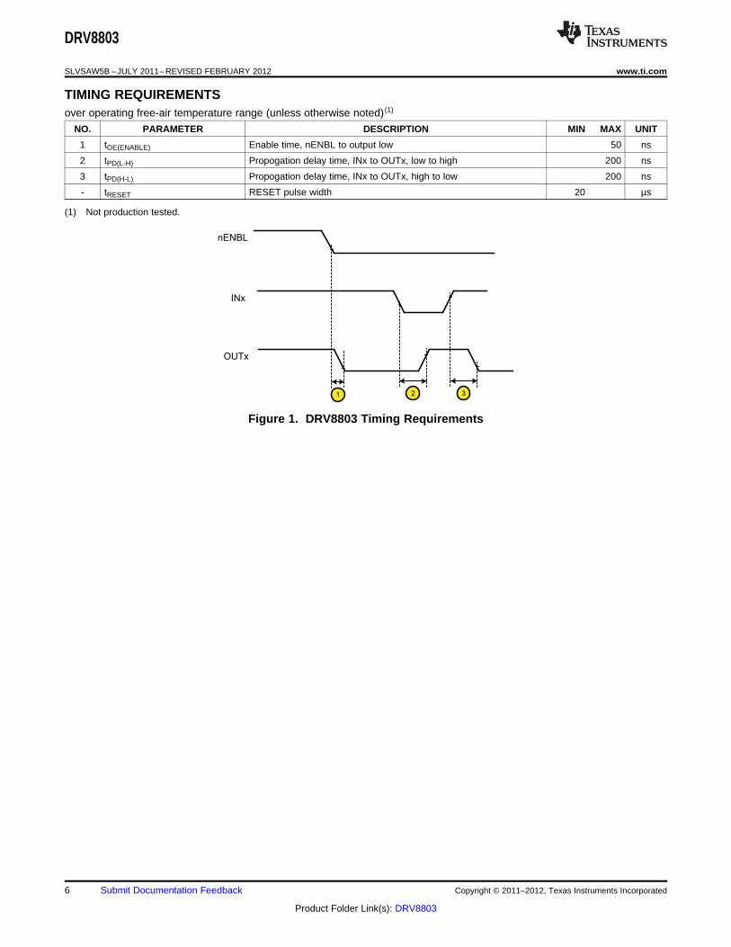
nENBL
INx
OUTx
21 3
DRV8803
SLVSAW5B –JULY 2011–REVISED FEBRUARY 2012 www.ti.com
TIMING REQUIREMENTSover operating free-air temperature range (unless otherwise noted) (1)
NO. PARAMETER DESCRIPTION MIN MAX UNIT
1 tOE(ENABLE) Enable time, nENBL to output low 50 ns
2 tPD(L-H) Propogation delay time, INx to OUTx, low to high 200 ns
3 tPD(H-L) Propogation delay time, INx to OUTx, high to low 200 ns
- tRESET RESET pulse width 20 µs
(1) Not production tested.
Figure 1. DRV8803 Timing Requirements
6 Submit Documentation Feedback Copyright © 2011–2012, Texas Instruments Incorporated
Product Folder Link(s): DRV8803
IN1
IN4
IN3
IN2
nENBL OUT1
OUT2
OUT3
OUT4
DRV8803
www.ti.com SLVSAW5B –JULY 2011–REVISED FEBRUARY 2012
FUNCTIONAL DESCRIPTION
Output Drivers
The DRV8803 contains four protected low-side drivers. Each output has an integrated clamp diode connected toa common pin, VCLAMP.
VCLAMP can be connected to the main power supply voltage, VM. It can also be connected to a zener or TVSdiode to VM, allowing the switch voltage to exceed the main supply voltage VM. This connection can bebeneficial when driving loads that require very fast current decay, such as unipolar stepper motors.
In all cases, the voltage on the outputs must not be allowed to exceed the maximum output voltage specification.
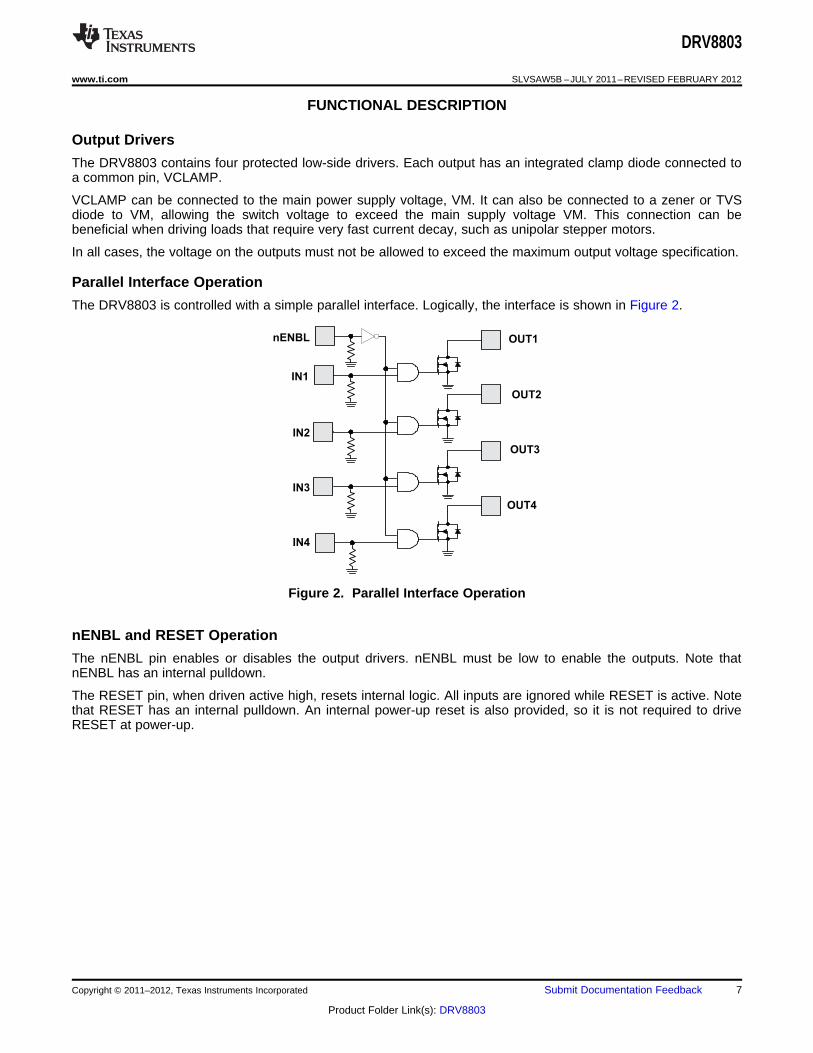
Parallel Interface Operation
The DRV8803 is controlled with a simple parallel interface. Logically, the interface is shown in Figure 2.
Figure 2. Parallel Interface Operation
nENBL and RESET Operation
The nENBL pin enables or disables the output drivers. nENBL must be low to enable the outputs. Note thatnENBL has an internal pulldown.
The RESET pin, when driven active high, resets internal logic. All inputs are ignored while RESET is active. Notethat RESET has an internal pulldown. An internal power-up reset is also provided, so it is not required to driveRESET at power-up.
Copyright © 2011–2012, Texas Instruments Incorporated Submit Documentation Feedback 7
Product Folder Link(s): DRV8803
DRV8803
SLVSAW5B –JULY 2011–REVISED FEBRUARY 2012 www.ti.com
Protection Circuits
The DRV8803 is fully protected against undervoltage, overcurrent and overtemperature events.
Overcurrent Protection (OCP)
An analog current limit circuit on each FET limits the current through the FET by removing the gate drive. If thisanalog current limit persists for longer than the tOCP deglitch time (approximately 3.5 µs), the driver will bedisabled and the nFAULT pin will be driven low. The driver will remain disabled for the tRETRY retry time(approximately 1.2 ms), then the fault will be automatically cleared. The fault will be cleared immediately if eitherRESET pin is activated or VM is removed and re-applied.
Thermal Shutdown (TSD)
If the die temperature exceeds safe limits, all output FETs will be disabled and the nFAULT pin will be driven low.Once the die temperature has fallen to a safe level, operation will automatically resume.
Undervoltage Lockout (UVLO)
If at any time the voltage on the VM pin falls below the undervoltage lockout threshold voltage, all circuitry in thedevice will be disabled, and internal logic will be reset. Operation will resume when VM rises above the UVLOthreshold.
8 Submit Documentation Feedback Copyright © 2011–2012, Texas Instruments Incorporated
Product Folder Link(s): DRV8803

P = RDS(ON) · (I )OUT
2
DRV8803
www.ti.com SLVSAW5B –JULY 2011–REVISED FEBRUARY 2012
THERMAL INFORMATION
Thermal Protection
The DRV8803 has thermal shutdown (TSD) as described above. If the die temperature exceeds approximately150°C, the device will be disabled until the temperature drops to a safe level.
Any tendency of the device to enter TSD is an indication of either excessive power dissipation, insufficientheatsinking, or too high an ambient temperature.
Power Dissipation
Power dissipation in the DRV8803 is dominated by the power dissipated in the output FET resistance, orRDS(ON). Average power dissipation of each FET when running a static load can be roughly estimated byEquation 1:
(1)
where P is the power dissipation of one FET, RDS(ON) is the resistance of each FET, and IOUT is equal to theaverage current drawn by the load. Note that at start-up and fault conditions this current is much higher thannormal running current; these peak currents and their duration also need to be taken into consideration. Whendriving more than one load simultaneously, the power in all active output stages must be summed.
The maximum amount of power that can be dissipated in the device is dependent on ambient temperature andheatsinking.
Note that RDS(ON) increases with temperature, so as the device heats, the power dissipation increases. This mustbe taken into consideration when sizing the heatsink.
Heatsinking
The DRV8803DW package uses a standard SOIC outline, but has the center pins internally fused to the die padin order to more efficiently remove heat from the device. The two center leads on each side of the packageshould be connected together to as large a copper area on the PCB as is possible to remove heat from thedevice. If the copper area is on the opposite side of the PCB from the device, thermal vias are used to transferthe heat between top and bottom layers.
In general, the more copper area that can be provided, the more power can be dissipated.
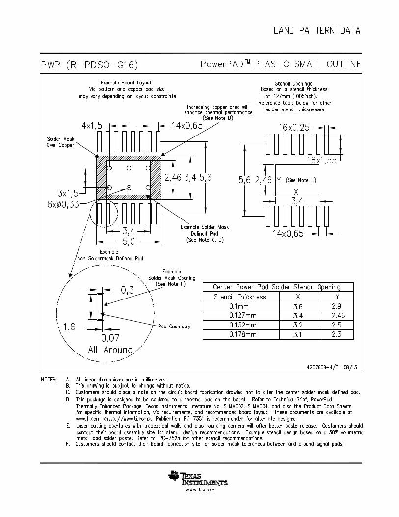
The DRV8803PWP package uses an HTSSOP package with an exposed PowerPAD™. The PowerPAD packageuses an exposed pad to remove heat from the device. For proper operation, this pad must be thermallyconnected to copper on the PCB to dissipate heat. On a multi-layer PCB with a ground plane, this can beaccomplished by adding a number of vias to connect the thermal pad to the ground plane. On PCBs withoutinternal planes, copper area can be added on either side of the PCB to dissipate heat. If the copper area is onthe opposite side of the PCB from the device, thermal vias are used to transfer the heat between top and bottomlayers.
For details about how to design the PCB, refer to TI Application Report SLMA002, "PowerPAD ThermallyEnhanced Package" and TI Application Brief SLMA004, "PowerPAD Made Easy", available at www.ti.com.
Copyright © 2011–2012, Texas Instruments Incorporated Submit Documentation Feedback 9
Product Folder Link(s): DRV8803
PACKAGE OPTION ADDENDUM
www.ti.com 11-Apr-2013
Addendum-Page 1
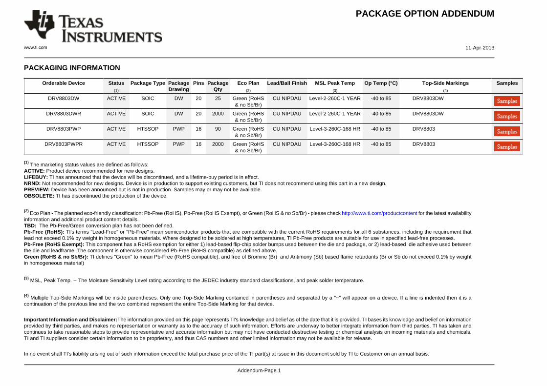
PACKAGING INFORMATION
Orderable Device Status(1)
Package Type PackageDrawing
Pins PackageQty
Eco Plan(2)
Lead/Ball Finish MSL Peak Temp(3)
Op Temp (°C) Top-Side Markings(4)
Samples
DRV8803DW ACTIVE SOIC DW 20 25 Green (RoHS& no Sb/Br)
CU NIPDAU Level-2-260C-1 YEAR -40 to 85 DRV8803DW
DRV8803DWR ACTIVE SOIC DW 20 2000 Green (RoHS& no Sb/Br)
CU NIPDAU Level-2-260C-1 YEAR -40 to 85 DRV8803DW
DRV8803PWP ACTIVE HTSSOP PWP 16 90 Green (RoHS& no Sb/Br)
CU NIPDAU Level-3-260C-168 HR -40 to 85 DRV8803
DRV8803PWPR ACTIVE HTSSOP PWP 16 2000 Green (RoHS& no Sb/Br)
CU NIPDAU Level-3-260C-168 HR -40 to 85 DRV8803
(1) The marketing status values are defined as follows:ACTIVE: Product device recommended for new designs.LIFEBUY: TI has announced that the device will be discontinued, and a lifetime-buy period is in effect.NRND: Not recommended for new designs. Device is in production to support existing customers, but TI does not recommend using this part in a new design.PREVIEW: Device has been announced but is not in production. Samples may or may not be available.OBSOLETE: TI has discontinued the production of the device.
(2) Eco Plan - The planned eco-friendly classification: Pb-Free (RoHS), Pb-Free (RoHS Exempt), or Green (RoHS & no Sb/Br) - please check http://www.ti.com/productcontent for the latest availabilityinformation and additional product content details.TBD: The Pb-Free/Green conversion plan has not been defined.Pb-Free (RoHS): TI's terms "Lead-Free" or "Pb-Free" mean semiconductor products that are compatible with the current RoHS requirements for all 6 substances, including the requirement thatlead not exceed 0.1% by weight in homogeneous materials. Where designed to be soldered at high temperatures, TI Pb-Free products are suitable for use in specified lead-free processes.Pb-Free (RoHS Exempt): This component has a RoHS exemption for either 1) lead-based flip-chip solder bumps used between the die and package, or 2) lead-based die adhesive used betweenthe die and leadframe. The component is otherwise considered Pb-Free (RoHS compatible) as defined above.Green (RoHS & no Sb/Br): TI defines "Green" to mean Pb-Free (RoHS compatible), and free of Bromine (Br) and Antimony (Sb) based flame retardants (Br or Sb do not exceed 0.1% by weightin homogeneous material)
(3) MSL, Peak Temp. -- The Moisture Sensitivity Level rating according to the JEDEC industry standard classifications, and peak solder temperature.
(4) Multiple Top-Side Markings will be inside parentheses. Only one Top-Side Marking contained in parentheses and separated by a "~" will appear on a device. If a line is indented then it is acontinuation of the previous line and the two combined represent the entire Top-Side Marking for that device.
Important Information and Disclaimer:The information provided on this page represents TI's knowledge and belief as of the date that it is provided. TI bases its knowledge and belief on informationprovided by third parties, and makes no representation or warranty as to the accuracy of such information. Efforts are underway to better integrate information from third parties. TI has taken andcontinues to take reasonable steps to provide representative and accurate information but may not have conducted destructive testing or chemical analysis on incoming materials and chemicals.TI and TI suppliers consider certain information to be proprietary, and thus CAS numbers and other limited information may not be available for release.
In no event shall TI's liability arising out of such information exceed the total purchase price of the TI part(s) at issue in this document sold by TI to Customer on an annual basis.

PACKAGE OPTION ADDENDUM
www.ti.com 11-Apr-2013
Addendum-Page 2
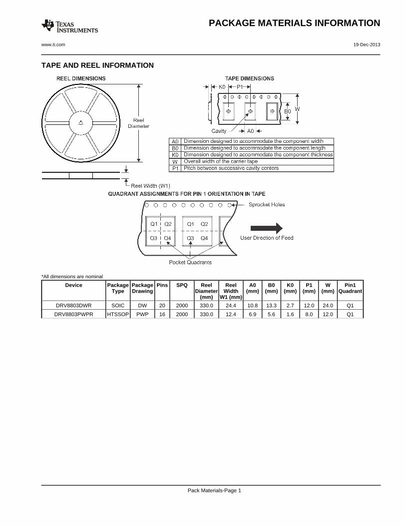
TAPE AND REEL INFORMATION
*All dimensions are nominal
Device PackageType
PackageDrawing
Pins SPQ ReelDiameter
(mm)
ReelWidth
W1 (mm)
A0(mm)
B0(mm)
K0(mm)
P1(mm)
W(mm)
Pin1Quadrant
DRV8803DWR SOIC DW 20 2000 330.0 24.4 10.8 13.3 2.7 12.0 24.0 Q1
DRV8803PWPR HTSSOP PWP 16 2000 330.0 12.4 6.9 5.6 1.6 8.0 12.0 Q1
PACKAGE MATERIALS INFORMATION
www.ti.com 19-Dec-2013
Pack Materials-Page 1

*All dimensions are nominal
Device Package Type Package Drawing Pins SPQ Length (mm) Width (mm) Height (mm)
DRV8803DWR SOIC DW 20 2000 367.0 367.0 45.0
DRV8803PWPR HTSSOP PWP 16 2000 367.0 367.0 35.0
PACKAGE MATERIALS INFORMATION
www.ti.com 19-Dec-2013
Pack Materials-Page 2


IMPORTANT NOTICETexas Instruments Incorporated and its subsidiaries (TI) reserve the right to make corrections, enhancements, improvements and otherchanges to its semiconductor products and services per JESD46, latest issue, and to discontinue any product or service per JESD48, latestissue. Buyers should obtain the latest relevant information before placing orders and should verify that such information is current andcomplete. All semiconductor products (also referred to herein as “components”) are sold subject to TI’s terms and conditions of salesupplied at the time of order acknowledgment.TI warrants performance of its components to the specifications applicable at the time of sale, in accordance with the warranty in TI’s termsand conditions of sale of semiconductor products. Testing and other quality control techniques are used to the extent TI deems necessaryto support this warranty. Except where mandated by applicable law, testing of all parameters of each component is not necessarilyperformed.TI assumes no liability for applications assistance or the design of Buyers’ products. Buyers are responsible for their products andapplications using TI components. To minimize the risks associated with Buyers’ products and applications, Buyers should provideadequate design and operating safeguards.TI does not warrant or represent that any license, either express or implied, is granted under any patent right, copyright, mask work right, orother intellectual property right relating to any combination, machine, or process in which TI components or services are used. Informationpublished by TI regarding third-party products or services does not constitute a license to use such products or services or a warranty orendorsement thereof. Use of such information may require a license from a third party under the patents or other intellectual property of thethird party, or a license from TI under the patents or other intellectual property of TI.Reproduction of significant portions of TI information in TI data books or data sheets is permissible only if reproduction is without alterationand is accompanied by all associated warranties, conditions, limitations, and notices. TI is not responsible or liable for such altereddocumentation. Information of third parties may be subject to additional restrictions.Resale of TI components or services with statements different from or beyond the parameters stated by TI for that component or servicevoids all express and any implied warranties for the associated TI component or service and is an unfair and deceptive business practice.TI is not responsible or liable for any such statements.Buyer acknowledges and agrees that it is solely responsible for compliance with all legal, regulatory and safety-related requirementsconcerning its products, and any use of TI components in its applications, notwithstanding any applications-related information or supportthat may be provided by TI. Buyer represents and agrees that it has all the necessary expertise to create and implement safeguards whichanticipate dangerous consequences of failures, monitor failures and their consequences, lessen the likelihood of failures that might causeharm and take appropriate remedial actions. Buyer will fully indemnify TI and its representatives against any damages arising out of the useof any TI components in safety-critical applications.In some cases, TI components may be promoted specifically to facilitate safety-related applications. With such components, TI’s goal is tohelp enable customers to design and create their own end-product solutions that meet applicable functional safety standards andrequirements. Nonetheless, such components are subject to these terms.No TI components are authorized for use in FDA Class III (or similar life-critical medical equipment) unless authorized officers of the partieshave executed a special agreement specifically governing such use.Only those TI components which TI has specifically designated as military grade or “enhanced plastic” are designed and intended for use inmilitary/aerospace applications or environments. Buyer acknowledges and agrees that any military or aerospace use of TI componentswhich have not been so designated is solely at the Buyer's risk, and that Buyer is solely responsible for compliance with all legal andregulatory requirements in connection with such use.TI has specifically designated certain components as meeting ISO/TS16949 requirements, mainly for automotive use. In any case of use ofnon-designated products, TI will not be responsible for any failure to meet ISO/TS16949.Products ApplicationsAudio www.ti.com/audio Automotive and Transportation www.ti.com/automotiveAmplifiers amplifier.ti.com Communications and Telecom www.ti.com/communicationsData Converters dataconverter.ti.com Computers and Peripherals www.ti.com/computersDLP® Products www.dlp.com Consumer Electronics www.ti.com/consumer-appsDSP dsp.ti.com Energy and Lighting www.ti.com/energyClocks and Timers www.ti.com/clocks Industrial www.ti.com/industrialInterface interface.ti.com Medical www.ti.com/medicalLogic logic.ti.com Security www.ti.com/securityPower Mgmt power.ti.com Space, Avionics and Defense www.ti.com/space-avionics-defenseMicrocontrollers microcontroller.ti.com Video and Imaging www.ti.com/videoRFID www.ti-rfid.comOMAP Applications Processors www.ti.com/omap TI E2E Community e2e.ti.comWireless Connectivity www.ti.com/wirelessconnectivity
Mailing Address: Texas Instruments, Post Office Box 655303, Dallas, Texas 75265Copyright © 2014, Texas Instruments Incorporated