qualification report - t3 mixer in cqg package · qualification report ‐ t3 mixer in cqg package...
TRANSCRIPT

Qualification Report T3 Mixer In CQG Package

Qualification Report ‐ T3 Mixer In CQG Package March 2017
2
Table of Contents Page
Introduction 6 CQG Package 8 Summary of Test Results 10 Summary of Performance Variation 10 Environmental / Operational Maximum Ratings 10 Environmental Test Plan 12 Electrical Test 14 Test Fixtures 14 MSL & Preconditioning 15 Performance Plots ‐ High Temperature Operation (HTO) 17 Performance Plots – Highly Accelerated Temperature and Humidity Stress Test (HAST) 19 Performance Plots – Autoclave (AC) 21 Performance Plots – High Temperature Storage Life (HTSL) 23 Performance Plots – Low Temperature Storage Life (LTSL) 23 Performance Plots – Temperature Cycle (TC) 27
Table of AbbreviationsMarki Microwave Incorporated MMI High Temperature Operation HTO Highly Accelerated Temperature and Humidity Stress Test HAST Autoclave AC High Temperature Storage Life HTSL Low Temperature Storage Life LTSL Temperature Cycle TC

Qualification Report ‐ T3 Mixer In CQG Package March 2017
3
Table of FiguresNumber Description Page(s)
1 Mechanical Drawing of CQG Package 82 Cross‐sectional drawing of typical QFN package with GaAs die 83 Custom Test Fixture (Soldered) 144 Annotated MSL & Preconditioning Reflow Profile 155 HTO ‐ Mean Conversion Loss Variation Plot
6 HTO ‐ Frequency & Cumulative Distribution of Conversion Loss Variation (single unit variation) 17
7 HTO – LO Return Loss Comparison 188 HTO ‐ RF Return Loss Comparison 189 HTO ‐ IF Return Loss Comparison 1810 UHAST ‐ Mean Conversion Loss Variation Plot 19
11 UHAST ‐ Frequency & Cumulative Distribution of Conversion Loss Variation (single unit variation) 19
12 UHAST ‐ LO Return Loss Comparison 2013 UHAST ‐ RF Return Loss Comparison 2014 UHAST ‐ IF Return Loss Comparison 2015 Autoclave ‐ Mean Conversion Loss Variation Plot 21
16 Autoclave – Frequency & Cumulative Distribution of Conversion Loss Variation (single unit variation) 21
17 Autoclave ‐ LO Return Loss Comparison 2218 Autoclave ‐ RF Return Loss Comparison 2219 Autoclave – IF Return Loss Comparison 2220 HTSL ‐ Mean Conversion Loss Variation Plot 23
21 HTSL ‐ Frequency & Cumulative Distribution of Conversion Loss Variation (single unit variation) 23
22 HTSL – LO Return Loss Comparison 2423 HTSL ‐ RF Return Loss Comparison 2424 HTSL ‐ IF Return Loss Comparison 2425 LTSL ‐ Mean Conversion Loss Variation Plot 25
26 LTSL ‐ Frequency & Cumulative Distribution of Conversion Loss Variation (single unit variation) 25
27 LTSL ‐ LO Return Loss Comparison 2628 LTSL ‐ RF Return Loss Comparison 2629 LTSL – IF Return Loss Comparison 2630 Temperature Cycle ‐ Mean Conversion Loss Variation Plot 27
31 Temperature Cycle ‐ Frequency & Cumulative Distribution of Conversion Loss Variation (single unit variation) 27
32 Temperature Cycle – LO Return Loss Comparison 2833 Temperature Cycle ‐ RF Return Loss Comparison 2834 Temperature Cycle ‐ IF Return Loss Comparison 28

Qualification Report ‐ T3 Mixer In CQG Package March 2017
4
Table of TablesNumber Description Page(s)
1 Qualified MMI Part Numbers 82 Summary of Test Results 103 Summary of Performance Variation 104 Environmental / Operational Maximum Ratings ‐ Device 105 Environmental / Operational Maximum Ratings ‐ Package 106 Test Method – CQG Substrate & Device Operation 127 Test Method – CQG & Device Packages 128 RF Test Frequency Bands and Input Power 149 Custom Test Fixtures – Materials Used 1410 HTO Test Parameters 1711 UHAST Test Parameters 1912 Autoclave Test Parameters 2113 HTSL Test Parameters 2314 LTSL Test Parameters 2515 TC Parameters 27

Qualification Report ‐ T3 Mixer In CQG Package March 2017
5
Introduction

Qualification Report ‐ T3 Mixer In CQG Package March 2017
6
Our reliability study combines device & package test methods to produce a comprehensive view of a typical component’s mechanical and electrical integrity over its lifetime. The conclusions drawn from this study establishes Marki Microwave’s CQ(G) package’s ability to withstand mechanical stresses that were imposed by the test methods. It also provides a basis of confidence in CQ(G) package’s ability to support the specified electrical performance of a typical Marki Microwave T3 mixer device contained within.
The test plan used to perform this study provides a basis of confidence in CQ(G) and T3 mixer device use by following two courses:
1) Use under MMI’s rated electrical specifications and elevated temperature for a prolonged period 2) Use of other broadly accepted test methods that highlight the efficacy of specific mechanical features of
CQ(G) & T3 mixer device packages and soldered connections
This study is based on the application of JEDEC standards. The conditions applied to each standard were chosen to encourage our customers’ increased confidence in our product’s efficacy under environmental conditions that exceed typical use cases.

Qualification Report ‐ T3 Mixer In CQG Package March 2017
7
CQG Package

Qualification Report ‐ T3 Mixer In CQG Package March 2017
8
The representative assembly used in our study was MMI’s CQG (Au finish) package containing a T3 mixer device.
T307LCQG
IRL
D/CMADE IN USA
.320[8.13]
.300[7.62]
.050[1.27]
.220
.050
[5.59]
[1.27]
Ø.060 Thru,4 PL
Plastic Cover
.200
.400
.160
[5.08]
[4.06]
[10.16]
.13 Max[3.3]
Figure 1 – An outline of T3‐08CQG. Alternate dimensioning: [ mm ]
Plastic Cover
MixerSoldered Connection
Sealing EpoxyCircuit Substrate
Figure 2 – A cross‐sectioned drawing of a typical CQ(G) package with an undefined mixer assembly and soldered
connections to the package substrate.
Qualification Vehicle Marki Microwave Part Number
T3‐03CQ(G) T3‐04CQ(G) T3‐05CQ(G) T3‐06CQ(G) T3‐07CQ(G)
Table 1
Qualified By Similarity
T3 and legacy mixer assemblies of frequency bands up to 10GHz are qualified by similarity of construction to withstand all environmental stress contained in this report. The severity of any single environmental condition or combination thereof is not to exceed what’s explicitly defined.

Qualification Report ‐ T3 Mixer In CQG Package March 2017
9
Summaries & Declarations

Qualification Report ‐ T3 Mixer In CQG Package March 2017
10
Summary of Test Results
Table 2
Summary of Performance Variation
Table 3
Environmental/Operational Maximum Ratings
Table 4
Table 5
Test Method Qty In Qty Out Fails Fail CriteriaHigh Temperature Operation (HT) 24 24 0 >1dB change in mean conversion loss Unbiased Highly Accelerated Stress Test (UHAST) 24 24 0 >1dB change in mean conversion loss High Temperature Storage Life (HTSL) 3 3 0 >1dB change in mean conversion loss Low Temperature Storage Life (HTSL) 3 3 0 >1dB change in mean conversion loss Accelerated Moisture Resistance (Autoclave) 24 24 0 >1dB change in mean conversion loss Temperature Cycle (TC) 24 24 0 >1dB change in mean conversion loss
Test Method RF/LO Band (GHz) IF Frequency (GHz)
Initial Mean CL (dB)
Max Change In Mean CL (dB)
CL Range (dB)
HTO 0.010 – 8.0 0.091 6.86 0.08 0.12 HAST 0.010 – 8.0 0.091 6.89 0.14 0.20 HTSL 0.010 – 8.0 0.091 6.92 0.01 0.02 Autoclave 0.010 – 8.0 0.091 6.85 0.14 0.20 Temperature Cycle 0.010 – 8.0 0.091 6.76 0.14 0.20
DeviceStatic Operating Temperature Range ‐55oC to +100oC Static Storage Temperature Range ‐40oC to +150oC
PackageStatic Operating Temperature Range ‐55oC to +100oC Static Storage Temperature Range ‐40oC to +150oC
Dynamic Operating Temperature Range +25oC to +75oC, +5oC/min ramp Humidity 80% RH @ +85oC

Qualification Report ‐ T3 Mixer In CQG Package March 2017
11
Test Plan

Qualification Report ‐ T3 Mixer In CQG Package March 2017
12
CQG Substrate & Device Operation Test Condition Duration Sample Size Fail Criteria
High Temperature Operation (HTO)
Ta = 130oC
fLO= 1.5GHz, PLo= +16dBm
1000 Hours 1 lot of 24 units >1dB change in mean conversion loss
Table 6
HTO: This test operates the semiconductor device and packaging with commonly used electrical parameters while subjecting the device and package to greater operational temperatures than specified on the applicable datasheet.
CQG & Device Packages Test Conditions Duration Sample Size Fail Criteria
Highly Accelerated Temperature and Humidity Stress Test, Unbiased (UHAST)
Temp = 130oC, RH = 85% Vapor Pressure = 33.3psia 96 Hours 1 lot of 24 units >1dB change in mean
conversion loss
High Temperature Storage Life (HTSL) Temp = 150oC 1000 Hours 1 lot of 3 units >1dB change in mean
conversion loss Low Temperature Storage Life (LTSL) Temp = ‐40oC 168 Hours 1 lot of 3 units >1dB change in mean
conversion loss Accelerated Moisture Resistance (Autoclave)
Temp = 121oC, RH = 100% Vapor Pressure = 29.7psia 96 Hours 1 lot of 24 units >1dB change in mean
conversion loss
Temperature Cycle (TC)
Ts (min) = ‐55oC Ts (max) = +100oCTransition Time = 31 minutes Dwell Time = 10 Minutes
500 Cycles 1 lot of 24 units >1dB change in mean conversion loss
Table 7
HAST: This test evaluates the reliability of non‐hermetic packaged devices in humid environments. It employs severe conditions of temperature, humidity, and bias which accelerate the penetration of moisture through the external protective material. The practice of this test procedure complied with JESD22‐A110D, Highly Accelerated Temperature and Humidity Stress Test**. HTSL: This test is typically used to determine the effects of time and temperature, under storage conditions, for thermally activated failure mechanisms and time‐to failure distributions of solid state electronic devices. The practice of this test procedure complied with JESD22‐A103D, High Temperature Storage Life**. LTSL: This test method is typically used to determine the effect of time and temperature, under storage conditions, for thermally activated failure mechanisms of solid state electronic devices. During the test, reduced temperature are used without electrical stress applied. This test was not destructive. The practice of this test procedure complied with JESD22‐A119A, Low Temperature Storage Life**. Autoclave: This test method applies primarily to moisture resistance evaluations and robustness testing. Samples are subjected to a condensing, highly humid atmosphere under pressure to force moisture into the package to uncover weaknesses such as delamination and metallization corrosion. The practice of this test procedure complied with JESD22‐A102D, Accelerated Moisture Resistance ‐ Unbiased Autoclave**. Temperature Cycling: This standard applies to single chamber temperature cycling and covers component and solder interconnection testing. This test is conducted to determine the ability of components and solder interconnects to withstand mechanical stresses induced by alternating high‐ and low‐temperature extremes. The practice of this test procedure complied with JESD22‐A104E, Temperature Cycling*.
* http://jedec.org/

Qualification Report ‐ T3 Mixer In CQG Package March 2017
13
Performance Testing & Preconditioning

Qualification Report ‐ T3 Mixer In CQG Package March 2017
14
Electrical Test All RF tests were performed using an electronically calibrated N5242A PNA‐X Network Analyzer. Table 8 shows the LO/RF/IF frequencies & input power.
LO/RF Band (GHz) LO Input Power (dBm) RF Input Power (dBm) IF Frequency (GHz)
0.010 – 8.0 +15 ‐15 0.091Table 8
Test Fixture
To facilitate RF testing, CQG package was attached to a custom designed test fixture. Table 9 gives a list of materials used in the construction of the test fixture.
Description / MaterialAluminum HousingSMA ConnectorRO 4003 PCBSilver EpoxySolder (SN63)
Table 9
T307LCQG
IRL
D/CMADE IN USA
Figure 3 – Custom test fixture designed to facilitate HTOL, HAST, HTSL & Autoclave tests.

Qualification Report ‐ T3 Mixer In CQG Package March 2017
15
Preconditioning & Moisture Sensitivity Level (MSL) All samples were subjected to preconditioning & MSL 1 conditions that comply with JESD22‐A113F, Preconditioning of Nonhermetic Surface Mount Devices Prior to Reliability Testing, & J‐STD‐020D.1, Moisture/Reflow Sensitivity Classification for Nonhermetic Solid State Surface Mount Devices. Both standards were met using the Pb‐free reflow parameters defined in J‐STD‐020D.1 and shown in figure 5.
Figure 4 – Pb‐free reflow profile used to precondition and set the moisture sensitivity level of all samples.

Qualification Report ‐ T3 Mixer In CQG Package March 2017
16
Performance Plots

Qualification Report ‐ T3 Mixer In CQG Package March 2017
17
High Temperature Operation (HTO)Conditions Duration Sample Size Fail Criteria Fails
Ta = 130o C, PLo= +16dBm
1000 Hours 1 lot of 24 units >1dB change in mean
conversion loss 0
Table 10
Purpose This test operates the semiconductor device and packaging with commonly used electrical parameters while subjecting the device and package to greater operational temperatures than specified on the applicable datasheet.
Conversion Loss Variation (HTO)
Figure 5 – Mean conversion loss variation vs duration of environmental stress among all samples.
Histogram and Cumulative Distribution of Conversion Loss Variation (HTO)
Figure 6 – Distribution of mean conversion loss variation gain among all samples; single unit RMS average.

Qualification Report ‐ T3 Mixer In CQG Package March 2017
18
LO Return Loss (HTO)
Figure 7 – Full band LO return loss comparison of 1 sample over 1000 hours of stress. RF Return Loss (HTO)
Figure 8 – Full band RF return loss comparison of 1 sample over 1000 hours of stress.
IF Return Loss (HTO)
Figure 9 – Full band IF return loss comparison of 1 sample over 1000 hours of stress.

Qualification Report ‐ T3 Mixer In CQG Package March 2017
19
Highly Accelerated Temperature and Humidity Stress Test, Unbiased (UHAST) Conditions Duration Sample Size Fail Criteria Fails
Temp = 130oC, RH = 85% Vapor Pressure = 33.3psia 96 Hours 1 lot of 24 units >1dB change in mean
conversion loss 0
Table 11
Purpose This test evaluates the reliability of non‐hermetic packaged devices in humid environments. It employs severe conditions of temperature, humidity, and bias which accelerate the penetration of moisture through the external protective material. The practice of this test procedure complied with JESD22‐A110D, Highly Accelerated Temperature and Humidity Stress Test.
Conversion Loss Variation (UHAST)
Figure 10 – Mean conversion loss variation vs duration of environmental stress among all samples.
Histogram and Cumulative Distribution of Conversion Loss Variation (UHAST)
Figure 11 – Distribution of mean conversion loss variation gain among all samples; single unit RMS average.

Qualification Report ‐ T3 Mixer In CQG Package March 2017
20
LO Return Loss (UHAST)
Figure 12 – Full band LO return loss comparison of 1 sample over 1000 hours of stress.
RF Return Loss (UHAST)
Figure 13 – Full band RF return loss comparison of 1 sample over 1000 hours of stress.
IF Return Loss (UHAST)
Figure 14 – Full band IF return loss comparison of 1 sample over 1000 hours of stress.

Qualification Report ‐ T3 Mixer In CQG Package March 2017
21
Accelerated Moisture Resistance (Autoclave) Conditions Duration Sample Size Fail Criteria Fails
Temp = 121oC, RH = 100% Vapor Pressure = 29.7psia 96 Hours 1 lot of 24 units >1dB change in mean
conversion loss 0
Table 12
Purpose This test method applies primarily to moisture resistance evaluations and robustness testing. Samples are subjected to a condensing, highly humid atmosphere under pressure to force moisture into the package to uncover weaknesses such as delamination and metallization corrosion. The practice of this test procedure complied with JESD22‐A102D, Accelerated Moisture Resistance ‐ Unbiased Autoclave.
Conversion Loss Variation (AC)
Figure 15 – Mean conversion loss variation vs duration of environmental stress among all samples.
Histogram and Cumulative Distribution of Conversion Loss Variation (AC)
Figure 16 – Distribution of mean conversion loss variation gain among all samples; single unit RMS average.

Qualification Report ‐ T3 Mixer In CQG Package March 2017
22
LO Return Loss (AC)
Figure 17 – Full band LO return loss comparison of 1 sample over 1000 hours of stress.
RF Return Loss (AC)
Figure 18 – Full band RF return loss comparison of 1 sample over 1000 hours of stress.
IF Return Loss (AC)
Figure 19 – Full band IF return loss comparison of 1 sample over 1000 hours of stress.

Qualification Report ‐ T3 Mixer In CQG Package March 2017
23
High Temperature Storage Life (HTSL) Conditions Duration Sample Size Fail Criteria Fails
Temp = 150oC 1000 Hours 1 lot of 3 units >1dB change in mean conversion loss 0
Table 13
Purpose This test is typically used to determine the effects of time and temperature, under storage conditions, for thermally activated failure mechanisms and time‐to failure distributions of solid state electronic devices. The practice of this test procedure complied with JESD22‐A103D, High Temperature Storage Life.
Conversion Loss Variation (HTSL)
Figure 20 – Mean conversion loss variation vs duration of environmental stress among all samples.
.
LO Return Loss (HTSL)
Figure 22 – Full band LO return loss comparison of 1 sample over 1000 hours of stress.

Qualification Report ‐ T3 Mixer In CQG Package March 2017
24
RF Return Loss (HTSL)
Figure 23 – Full band RF return loss comparison of 1 sample over 1000 hours of stress.
IF Return Loss (HTSL)
Figure 24 – Full band IF return loss comparison of 1 sample over 1000 hours of stress.

Qualification Report ‐ T3 Mixer In CQG Package March 2017
25
Low Temperature Storage Life (LTSL) Conditions Duration Sample Size Fail Criteria Fails
Temp = ‐40oC 168 Hours 1 lot of 3 units >1dB change in mean conversion loss 0
Table 14
Purpose This test method is typically used to determine the effect of time and temperature, under storage conditions, for thermally activated failure mechanisms of solid state electronic devices. During the test, reduced temperature are used without electrical stress applied. This test was not destructive. The practice of this test procedure complied with JESD22‐A119A, Low Temperature Storage Life**.
Conversion Loss Variation (LTSL)
Figure 25 – Mean conversion loss variation vs duration of environmental stress among all samples.
LO Return Loss (LTSL)
Figure 27 – Full band LO return loss comparison of 1 sample over 1000 hours of stress.

Qualification Report ‐ T3 Mixer In CQG Package March 2017
26
RF Return Loss (LTSL)
Figure 28 – Full band RF return loss comparison of 1 sample over 1000 hours of stress.
IF Return Loss (LTSL)
Figure 29 – Full band IF return loss comparison of 1 sample over 1000 hours of stress.
Qualification Report ‐ T3 Mixer In CQG Package March 2017
27
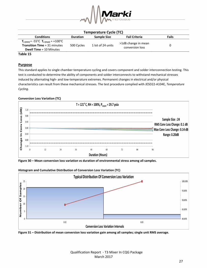
Temperature Cycle (TC) Conditions Duration Sample Size Fail Criteria Fails
Ts (min) = ‐55oC Ts (max) = +100oC Transition Time = 31 minutes Dwell Time = 10 Minutes
500 Cycles 1 lot of 24 units >1dB change in mean conversion loss 0
Table 15
Purpose This standard applies to single chamber temperature cycling and covers component and solder interconnection testing. This test is conducted to determine the ability of components and solder interconnects to withstand mechanical stresses induced by alternating high‐ and low‐temperature extremes. Permanent changes in electrical and/or physical characteristics can result from these mechanical stresses. The test procedure complied with JESD22‐A104E, Temperature Cycling.
Conversion Loss Variation (TC)
Figure 30 – Mean conversion loss variation vs duration of environmental stress among all samples.
Histogram and Cumulative Distribution of Conversion Loss Variation (TC)
Figure 31 – Distribution of mean conversion loss variation gain among all samples; single unit RMS average.

Qualification Report ‐ T3 Mixer In CQG Package March 2017
28
LO Return Loss (TC)
Figure 32 – Full band LO return loss comparison of 1 sample over 1000 hours of stress.
RF Return Loss (TC)
Figure 33 – Full band RF return loss comparison of 1 sample over 1000 hours of stress.
IF Return Loss (TC)
Figure 34 – Full band IF return loss comparison of 1 sample over 1000 hours of stress.