quanta 3d 200i · 2013-12-10 · quanta 3d 200i will enable your laboratory to explore a new ... we...
TRANSCRIPT

P R O D U C T D A T A
The Quanta 3D 200i is a characterization instrument designed
to examine materials, conduct failure analysis and prepare
samples in an industrial or academic environment. Combining
Quanta scanning electron microscope (SEM) with a high
current focused ion beam (FIB), creates a versatile solution for
characterizing and modifying materials that is easy to use and
has the flexibility to handle any sample type.
The current-boosted tungsten SEM provides excellent imaging
capability for sub-micron structures while the high current ion
column can be used to precisely prepare a sample by removing
or depositing material at a rapid rate in small defined areas. The
Quanta 3D 200i will enable your laboratory to explore a new
way of fast sample preparation, 3D nanoanalysis, TEM, EBSD
& atom probe sample preparation or structural modification of
sample surfaces at the nanometer scale.
The Quanta 3D is based on the experience of FEI engineering
for ESEM and DualBeamTM systems. Integrating these two
leading technologies, combined with FEI’s automation software
like; AutoSlice and ViewTMSlice and ViewTMSlice and View (automated serial slicing) application,
AutoTEMTM for unattended preparation of multiple sections or
thin sample and proprietary gas chemistries for high volume
milling applications, deposition of insulators or conductors and
customized detector geometries for imaging of FIB prepared
sections makes Quanta 3D the ideal solution for 3D
nanocharacterization, 3D nanoprototyping, and in situ
nanoprocesses.
Featuring three imaging modes – high vacuum, low vacuum
and ESEMTM it can accommodate the widest range of samples of
any SEM system. A 'charge neutralization' mode is integrated for
working with FIB on insulating samples.
Quanta 3D provides you with an easy to use solution for the
investigation and preparation of all samples. Helping you to get
more data from any sample.
Key benefits
• Increase your imaging and analysis capabilities: collect
surface and subsurface information and reconstruct
imaging and analytical data in 3 dimensions
• Increase sample throughput and mill larger areas using
Quanta’s high current FIB for fast material removal
• Enhance nanocharacterization capabilities with 2 kV
cleaning of TEM/atom probe/EBSD samples; reducing the
amorphous region without argon cleaning
• Improve pattern registration/nanoprototyping of non-
conductive samples with 'charge neutralization' mode
• Increase your sample thruput with automated recipes for
unattended FIB sectioning or TEM sample preparation
• Explore a wider range of materials with the larger working
distance at the coincidence point; enabling more detector
options and system flexibility for odd-shaped samples or
cutting edge experiments
• Increase flexibility characterizing specimens in a dynamic
environment; keep samples wet or perform heating
experiments with ESEM
Quanta™ 3D 200iExplore a new world of sub-micron sample preparation, modification and 3D inspection
Any sample, all data,any dimension

P R O D U C T D A T A
Some typical application examples are:
• TEM, atom probe or EBSD sample preparation
• Atom probe sample preparation
• Reveal the sub-surface cause of surface defects on finished
metal surfaces (e.g. painted surfaces, galvanized surfaces)
• 3D porosity characterization and quantification
• Site specific sectioning for ex-situ characterization with
other lab tools
• Volumetric reconstruction of the distribution of carbide
inclusions in steel
• Crack tip 3D reconstruction
• Reveal the sub-surface cause of surface defects on finished
metal surfaces (e.g. painted surfaces, galvanized surfaces)
• Characterization of strained materials along orthogonal
sections
• Micro-volume sample biopsies
• Wetting behavior characterization and dihedral angle
measurements
• Basic circuit edit
• Structural modification of surfaces at the nm-scale
(nanoprototyping)
Figure 2: Cross section of artifact buried below the surface.Figure 1: TEM lamella prepared from TiO2/Au/Silical sample.
Essential specifications
Electron optics
• Thermal emission SEM optics, with dual-anode source
emission geometry, fixed objective lens final aperture and
through the lens differential pumping
• Typical filament lifetime > 100 hours
• Resolution:
– 3.0 nm @ 30 kV @ high vacuum mode
– 3.0 nm @ 30 kV @ ESEM mode
– < 12 nm @ 3 kV @ low vacuum mode
• Max. horizontal field width:
10 mm corresponds to approx.
10 x magnification in quad view
• Accelerating voltage: 200 V to 30 kV
• Probe current: up to 1 µA – continuously variable
• 'charge neutralization' mode for milling of non-conductive
samples
Ion optics
• High current ion column with Ga liquid metal ion source
• Source lifetime: 1000 hours guaranteed
• Resolution at beam coincidence point: 9 nm @ 30 kV @ 1 pA
• Resolution at optimum FIB working distance:
7 nm @ 30 kV @ 1 pA
• Max. horizontal field width: 2.5 mm at 10 kV and beams
coincidence point (corresponds to 50 x minimum
magnification in quad view)
• Accelerating voltage: 2 to 30 kV
• Probe current: 1 pA to 65 nA in 15 steps
• Beam blanker standard, external control possible
• 15 position aperture strip
Vacuum system
• 1 x 250 l/s TMP oil free
• 2 x PVP oil free (scroll pumps)

P R O D U C T D A T A
• 1 x IGP (for ion column)
• Evacuation time (high vacuum): < 3.5 minutes
• Three vacuum modes: high vacuum, low vacuum and ESEM
• Seamless transition between high and low vacuum
• Through the lens differential pumping design for short beam
gas path lengths and ultra-low chamber vacuum (2600 Pa)
• Imaging gas in low vacuum and ESEM: water vapor or other
auxiliary gas (subject to FEI approval)
Detectors
• Everhart Thornley SED
• Large field Gaseous SED (used in low vacuum)
• Gaseous SED (used in ESEM mode)
• IR-CCD
• TV-rate solid-state BSED*
• STEM detector*
• Second IR-CCD*
• Gaseous analytical BSED (used for low vacuum
analytical applications)*
• Ion detector (CDEM)*
Digital image processor
• Dwell: 50 ns to 25 ms adjustable in steps of 100 ns
• Up to 4096 x 3536 pixel resolution
• File type: TIFF (8, 16 or 24 bit), BMP, JPG or AVI
• Single frame or 4-quadrant image display
• 4-quadrant live with independant digital zoom per quadrant
• 256 frame average or integration
• Image mixing of 2 or 3 images live (grey or false color)
• Movie recorder (direct to AVI)
• Movie creator (to make movies from tiff series)
Chamber
• 379 mm left to right
• 16 ports
• 15 mm electron and ion-beam coincidence point =
analytical WD
• Angle between e-column and
I-column: 52 degrees
5-axis motorized stage
• Eucentric goniometer stage
• x = 50 mm
• y – 50 mm
• z = 25 mm
• Clearance = max. 30 mm to eucentric point
• T = -10 to 60 degrees
• R = n x 360 degrees
Gas chemistry*
• 'Zero-collision' GIS design concept
– Individual gas injectors with separate injection
systems reconfigurable in the future
– 5 µm placing accuracy without user interaction
– GIS control available for automation
• Up to 3 gas injectors for enhanced etch or deposition*
• Gas chemistry options:*
– Platinum metal deposition*
– Tungsten metal deposition*
– Carbon deposition*
– Gold deposition*
– Insulator enhanced etch (XeF2)*
– Selective Carbon Mill*
– Enhanced etch*
System control
• 32 bit graphical user interface with Windows XP,
keyboard, optical mouse
• Image display: 19 inch LCD, SVGA 1280 x 1024
• Support computer
• Scripting interface for automation purposes*
• Multifunctional control panel*
• 2nd monitor (for support computer)*
• Joystick*
* optional
Figure 3: GIS injector port allocation.Figure 3: GIS injector port allocation.
GIS1
GIS2
GIS3GIS3GIS3
P R O D U C T D A T A
©2008. We are constantly improving the performance of our products, so all
specifications are subject to change without notice. The FEI logo, AutoTEM,
AutoFIB, DualBeam, ESEM, AutoSlice & View, Quanta and Tools for Nanotech are
trademarks of FEI Company. Windows is a trademark of Microsoft Corporation.
04DS-DB0114 08/08
WORLD HEADQUARTERS5350 NE DAWSON CREEK DRIVEHILLSBORO, OREGON 97124 USAPH: +1.503.726.7500
FEI EUROPEPH: +31.40.23.56000
FEI JAPANPH: +81.3.3740.0970
FEI ASIA PACIFICPH: +86.21.5027.8805
fei.com
TÜV Certification for design, manufacture,installation and support of focused ion-and electron-beam microscopes forthe NanoElectronics, NanoBiology,NanoResearch and Industry markets.
Common system options
• Serial sectioning automation software (AutoSlice and ViewTMSlice and ViewTMSlice and View )
• Automation software for multi-site milling (AutoFIBTM)
• Automation software for unattended TEM sample
preparation (AutoTEM)
• 3D reconstruction software
• Image analysis and archive software
• SW controlled Peltier cooled specimen stage
• SW controlled WetSTEM system
• SW controlled 1000 °C heating stage
• Remote control SW
• Video printer
• Specimen holder kit, TEM specimen holder kit
• Gas injectors
• BSED detector
• STEM detector
• Fast electrostatic electron beam blanker
• Supplies (compressor, mains matching
transformer, UPS)
• Omniprobe for in situ TEM sample lift-outin situ TEM sample lift-outin situ
• Cryo system
• Quick Loader (load lock)
• EDX
• EBSD
• WDX
Consumables
• Replacement Ga ion source
• Aperture strip for ion column
• Tungsten filaments
• Final lens apertures
• Gas chemistry refill packages
Installation requirements
• Power: voltage 230 V (-6 % + 10 %)
• Frequency: 50 or 60 Hz (+/- 1%)
• Power consumption: < 3.0 kVA for basic microscope
• Environment: temperature 20 °C +/- 3 °C, temperature
stability < 1 degree/hour, relative humidity below 80%,
stray AC magnetic fields < 100 nT a-synchronous,
< 300 nT synchronous
• Door width: 90 cm
• Weight: column console 550 kg
• Compressed air 4 to 6 bar, clean, dry and oil free
Documentation
• Operating instructions on CD
• On-line help
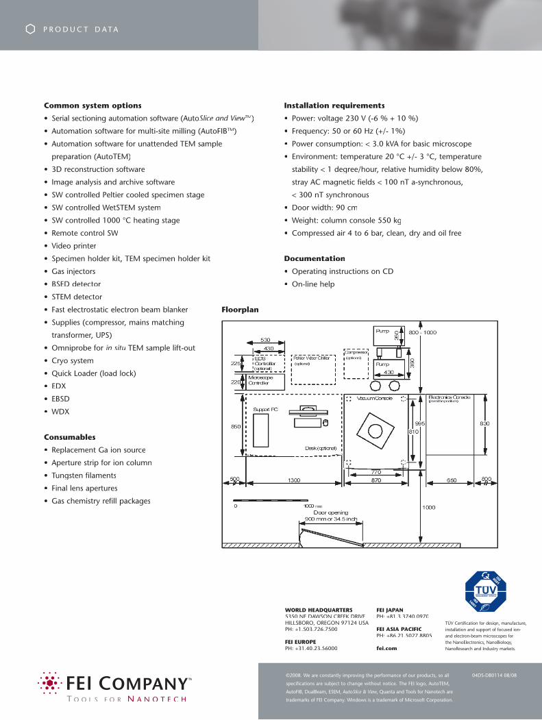
Floorplan