question kurukshetra i roll no. - t,s-: theory examination
TRANSCRIPT
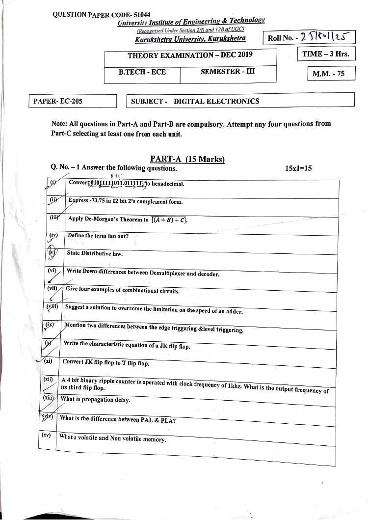
QUESTION PAPER CODE- 51044 · Universitv Institute o( Engineering & Technology,
(Recognised Under Section 1(0 and I 2B of UGC) ..-------:::=::--:--~---::-,I Kurukshetra University, Kurukshetra I Roll No. - 2 fltl) 1 \ t,S-:
THEORY EXAMINATION -DEC 2019 j TIME-3 Hrs. I B.TECH - ECE ' I SEMESTER-ID M.M.-75 I
..__P AP_E_R_-_E_c_-2_os ___ __,I I SUBJECT - DIGIT AL ELECTRONICS
Note: All questions in Part-A and Part-Bare compulsory. Attempt any four questions from Part-C selecting at least one from each unit.
......
PART-A (15 Marks) Q. No. -1 Answer the following questions.
./ 'll. l.
' ;JV Conve~OJ.!Y 101 !,OllJ !ll}o hexadecimal.
.,,
. IJ!iY ~ ess -73.75 in 12 bit 2's complement form. /
(iii( Apply De-Morgan's Theorem to [(A+ B) + CJ.
(iv) ,/
Define the term fan out? ,c... 1/(f State Distributive law.
/ Write Down differences between Demultiplexer and decoder. / (7 Give four examples of combinational circuits.
v (v. .. ,
Suggest a solution to overcome the limitation on the speed of an adder. ,
p: ~ention_ two differences between the edge triggering &level triggering. /
I~ Write the characteristic equation of a JK flip flop.
VCxi) Convert JK flip flop to T flip flop .
(xii) ,
15x1=15
-- ---
/ 4 ~it bi~ary ripple counter is operated with clock frequency of lkh Wh . its third flip flop. z. at 1s the output frequency of
V, What is propagation delay. V . -~ What is the difference between PAL & PLA?
(xv) Whats volatile and Non volatile memory.
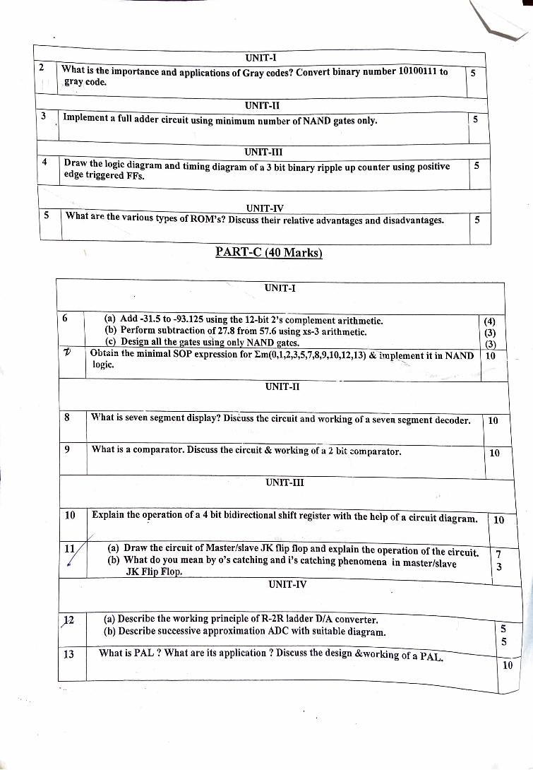
UNIT-I 2 What is the importance and applications of Gray codes? Convert binary number 10100111 to 15
,gray code.
UNIT-II 3 Implement a full adder circuit using minimum number of NANO gates only. \ 5
\
I UNIT-Ill
4 Draw the logic diagram and timing diagram of a 3 bit binary ripple up counter using positive 5 edge triggered FFs.
UNIT-IV 5 What are the various types ofROM's? Discuss their relative advantages and disadvantages. 5
PART-C {40 Marks)
UNIT-I
6 (a) Add -31.5 to -93.125 using the 12-bit 2's complement arithmetic. (4) (b) Perform subtraction of 27.8 from 57.6 using xs-3 arithmetic. (3) (c) Design all the gates us1ng only NAND gates. (3)
1) Obtain the minimal SOP expression for I.m(0,1,2,3,5,7,8,9,10,12,13) &'1mpl,t,ment it in NAND 10 -logic. -. ..
UNIT-II
8 ·what is seven segment display? Discuss the circuit and working of a seven segment decoder. 10
9 What is a comparator. Discuss the circuit & working of a 2 bit ;;omparator. 10
UNIT-III I
10 Explain the operation of a 4 bit bidirectional shift register with the help of a circuit diagram. 10 V
3/ (a) Draw the circuit of Master/slave JK flip flop and explain the operation of the circuit. 7 (b) What do you mean by o's catching and i's catching phenomena in master/slave 3 JK Flip Flop. UNIT-IV
}'2 (a) Describe the working principle of R-2R ladder DIA converter. 5 (b) Describe successive approximation ADC with suitable diagram. 5
13 What is PAL? What are its application? Discuss the design &working of a PAL. -~ 10
-
.. ---