r. w. ericksonecen5797/course_material/lecture42.pdftransistor on comparator turns transistor off...
TRANSCRIPT
R. W. EricksonDepartment of Electrical, Computer, and Energy Engineering
University of Colorado, Boulder

ECEN5807, Spring 2007
Power Electronics Program at CU Boulder
ECEN 4/5797 Introduction to Power
Electronics
ECEN5807Modeling and Control of PE
ECEN5817Resonant and Soft-Switching
ECEN 4/5517 Power Electronics Lab
Fall semesters
Spring semesters
Techniques in PEAlternate Spring semesters (2020)
SystemsAlternate Spring semesters (2019) Professional
Certificate in Power
Electronics

ECEN 5807, Spring 2015 2
Power Electronics Courses at the University of Colorado, Boulder
ECEN 2260 Circuits 2
ECEN 3250 Circuits 3
ECEN3170 Energy Conversion
ECEN 4797/5797 Intro to Power Electr.
ECEN 5807 Modeling and Control of
Power Electronics Systems
ECEN 5817 Res. and Soft-Sw. Tech
ECEN 4517/5517 Power Electronics Lab
ECEN 4827/5827 Analog IC Design
ECEN 5837 Mixed-Signal IC Design
ECEN 4167/5737 Energy Conversion 2
ECEN 5737 AC Drives
graduateundergraduate
ECEN 2250 Circuits 1
ECEN 5017 Pwr Elect for Electric
Drive Vehicles
Professional certificate in power electronics
Graduate certificate in electric drivetrain technology
Power management
Coursera (MOOC): Introduction to Power Electronics
Prerequisite for either ECEN 5807 or ECEN 5817: ECEN 5797
Power Electronics Laboratory Lecture 11
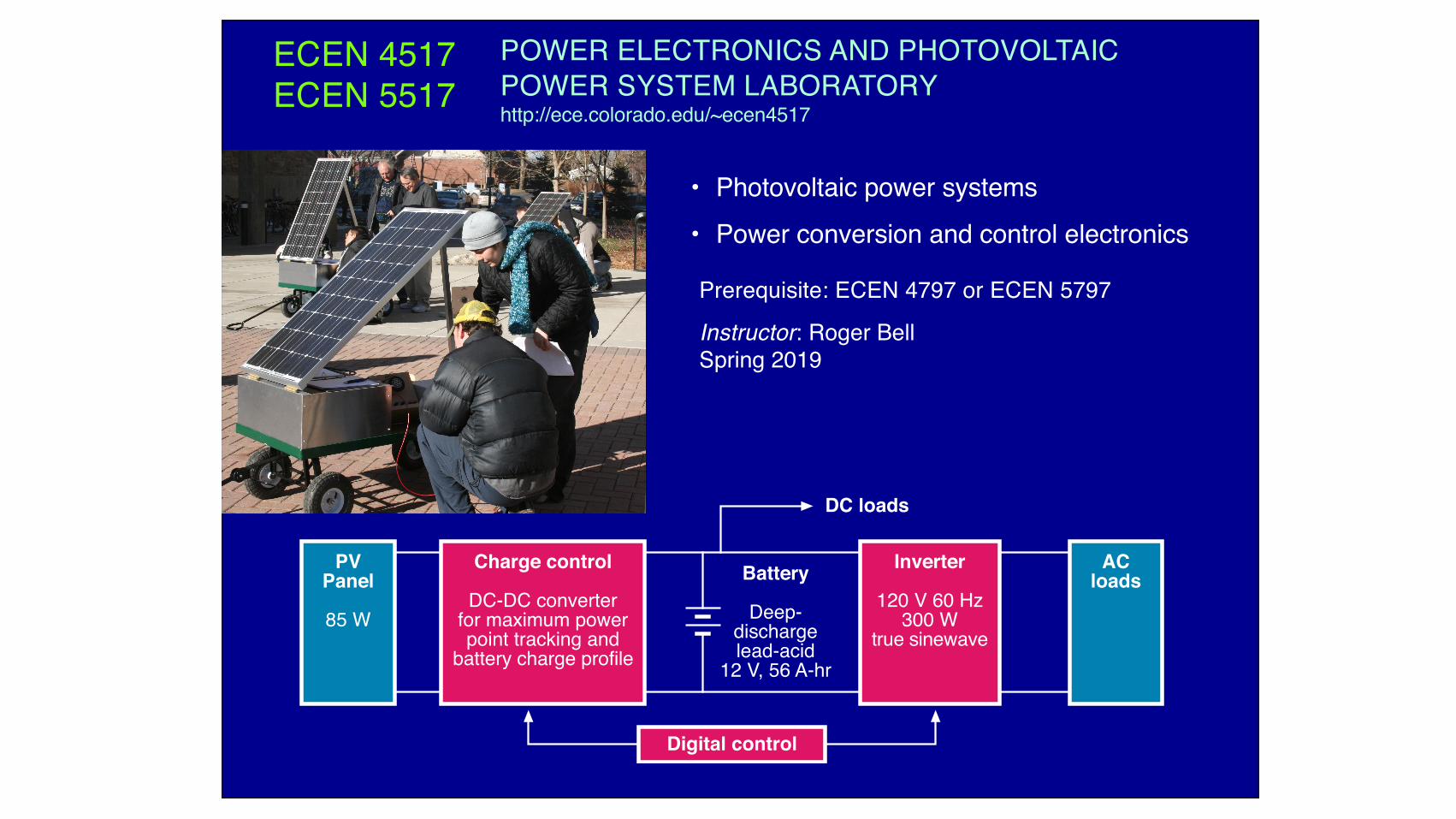
ECEN 4517ECEN 5517
POWER ELECTRONICS AND PHOTOVOLTAIC POWER SYSTEM LABORATORYhttp://ece.colorado.edu/~ecen4517
• Photovoltaic power systems• Power conversion and control electronics
PVPanel
85 W
Battery
Deep-dischargelead-acid
12 V, 56 A-hr
Inverter
120 V 60 Hz300 W
true sinewave
Charge control
DC-DC converterfor maximum powerpoint tracking and
battery charge profile
ACloads
DC loads
Digital control
Prerequisite: ECEN 4797 or ECEN 5797
Instructor: Roger BellSpring 2019
Power Electronics Laboratory Lecture 12
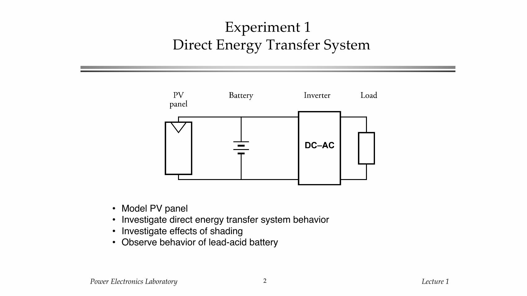
Experiment 1Direct Energy Transfer System
• Model PV panel• Investigate direct energy transfer system behavior• Investigate effects of shading• Observe behavior of lead-acid battery

Power Electronics Laboratory Lecture 13
Experiments 2 and 3Maximum Power Point Tracking
• Design and construct dc-dc converter• Employ microcontroller to achieve maximum power point tracking
(MPPT) and battery charge control

Power Electronics Laboratory Lecture 14
Experiments 4 and 5Add Inverter to System
• Build your own inverter system to drive AC loads from your battery• Step up the battery voltage to 200 VDC as needed by inverter• Regulate the 200 VDC with an analog feedback loop• Change the 200 VDC into 120 VAC

Power Electronics Laboratory Lecture 15
Mini-ProjectECEE Expo Competition
• Operate yourcomplete system
• Competition duringECEE Expo: capturethe most energy withyour system outside
Solar PowerCompetition and Expo
Awards given to the stand-alone solar power system demonstrating the highest efficiency and energy capture
Featuring Photovoltaics and
Power Electronics Laboratory
Classes ECEN 4517 and 5517
Thursday 4/30 9 a.m. to noon Herbst Plaza, CU Engr Center
A previous year’s competition poster

ECEN 5807 Topics
1. Simulation and averaged switch modeling• CCM, DCM, and other examples• Simulation
2. Techniques of design-oriented analysis, with application to switched-mode converter systems• Middlebrook’s feedback and extra-element theorems• Input filter design• Writing complex transfer function expressions by inspection
3. Current-programmed control of PWM converters4. Introduction to digital control of PWM converters5. Rectifiers
• Rectifier harmonics in power systems• Low-harmonic rectifiers and power factor correction converters
Spring 2019 Instructor: Prof. Dragan Maksimovic

ECEN 5807, Spring 2015 6
1. Simulation and Averaged Switch Modeling
• Additional notes, Section 7.4, Chapter 11, and Appendix B• Averaged switch modeling is another approach to derive the averaged model of a PWM
converter.• Well suited to Spice modeling of PWM converters• We will use this approach to model CCM, DCM, and current-programmed converters• Also useful for incorporation of ac losses (switching loss, core loss) into averaged models of PWM converters
• Computer simulation of small-signal transfer functions• Objectives of simulation• Spice models• Matlab/Simulink models

ECEN 5807, Spring 2015 7
Averaged Switch Modeling and Simulation
ECEN5807, Spring 2007

ECEN 5807, Spring 2015 8
2. Techniques of Design-Oriented Analysis
Chapter 10, Appendix C, and supplementary notes on websiteNull double injection methods for analysis of complex analog systems• Converter applications
Input filter design
Exact analysis of a fifth-order converter system
• Middlebrook’s extra element theoremHow to easily determine the effect of an added element on a circuit transfer function, without starting the analysis all over again
• The n extra element theoremHow to write complicated transfer functions by inspection, in rational form
• Middlebrook’s feedback theoremHow to easily construct the loop gain and transfer functions of a complex feedback circuit
ECEN 5807, Spring 2015 9
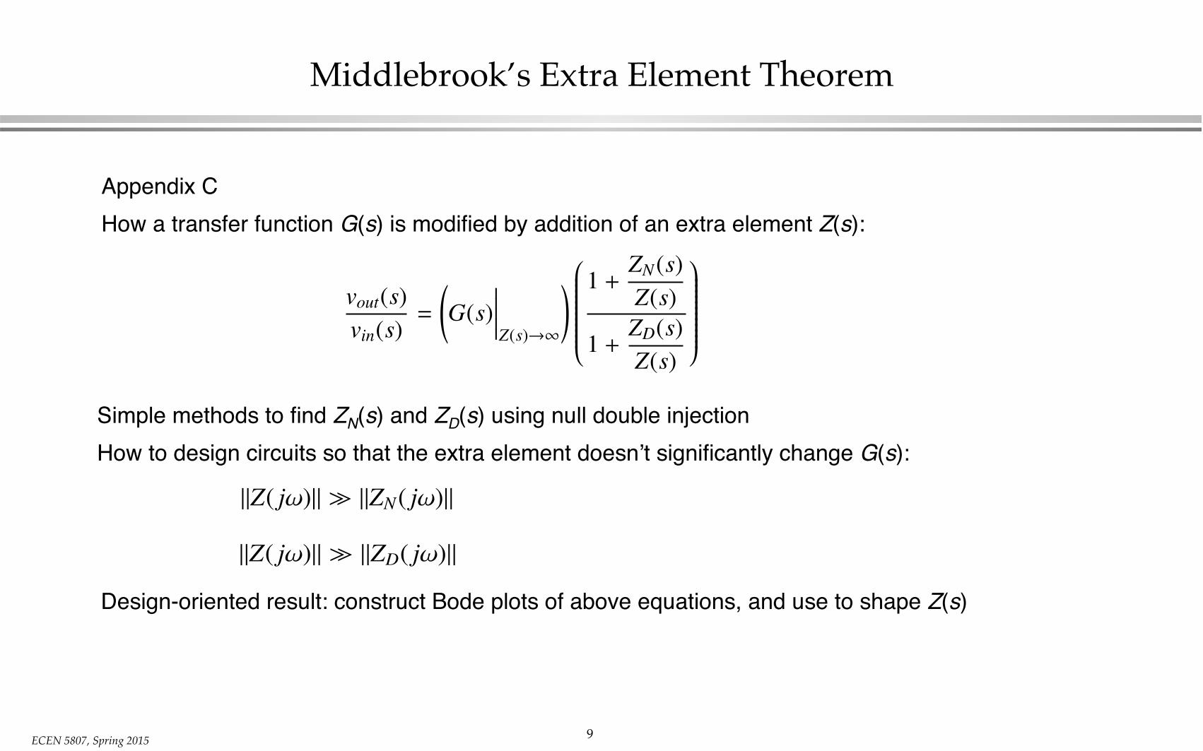
Middlebrook’s Extra Element Theorem
Appendix CHow a transfer function G(s) is modified by addition of an extra element Z(s):
Transistor voltage:
v
Q1(t) = V
Q1 + v
Q1(t)
where V
Q1 = hvQ1(t)i (dc component)
and hvQ1(t)i = 0 (v
Q1(t) is the ac component)
Similarly, the transistor current is
i
Q1(t) = I
Q1 + i
Q1(t)
The power p
Q
(t) flowing into the transistor is:
p
Q
(t) = v
Q1(t)iQ1(t) = 0 =
�V
Q1 + v
Q1(t)� ⇣
I
Q1 + i
Q1(t)⌘
Now multiply out and average over one period:
0 = V
Q1I
Q1 + hvQ1(t)iQ1(t)i
The transistor “consumes” power at DC,
and “generates” power at the switching
frequency. The transistor functions as an
inverter.
V
Q1I
Q1 = �hvQ1(t)iQ1(t)i
v
out
(s)v
in
(s)=
G(s)
�����Z(s)!1
!0BBBBBBBBBBBB@
1 +Z
N
(s)Z(s)
1 +Z
D
(s)Z(s)
1CCCCCCCCCCCCA
1
Simple methods to find ZN(s) and ZD(s) using null double injectionHow to design circuits so that the extra element doesn’t significantly change G(s):
Transistor voltage:
v
Q1(t) = V
Q1 + v
Q1(t)
where V
Q1 = hvQ1(t)i (dc component)
and hvQ1(t)i = 0 (v
Q1(t) is the ac component)
Similarly, the transistor current is
i
Q1(t) = I
Q1 + i
Q1(t)
The power p
Q
(t) flowing into the transistor is:
p
Q
(t) = v
Q1(t)iQ1(t) = 0 =
�V
Q1 + v
Q1(t)� ⇣
I
Q1 + i
Q1(t)⌘
Now multiply out and average over one period:
0 = V
Q1I
Q1 + hvQ1(t)iQ1(t)i
The transistor “consumes” power at DC,
and “generates” power at the switching
frequency. The transistor functions as an
inverter.
V
Q1I
Q1 = �hvQ1(t)iQ1(t)i
v
out
(s)v
in
(s)=
G(s)
�����Z(s)!1
!0BBBBBBBBBBBB@
1 +Z
N
(s)Z(s)
1 +Z
D
(s)Z(s)
1CCCCCCCCCCCCA
kZ( j!)k � kZN
( j!)k kZ( j!)k � kZD
( j!)k
1
Design-oriented result: construct Bode plots of above equations, and use to shape Z(s)

ECEN 5807, Spring 2015 10
Input Filter Design
ECEN 5807 : Introduction� 8�
Input filter design�
•� Filter can seriously degrade converter control system behavior�
•� Use extra element theorem to derive conditions which ensure that converter dynamics are not affected by input filter�
•� Must design input filter having adequate damping�
+–
Inputfilter
Converter
T(s)
Controller
vgZo(s) Zi(s)
H(s)
d
v
f
�� Gvd �� � Gvd
0˚
– 360˚
– 540˚
0 dB
– 10 dB
20 dB
30 dB
100 Hz
40 dB
1 kHz 10 kHz
– 180˚
10 dB
�� Gvd ��
� Gvd
• Input filter can seriously degrade control system behavior and cause instability
• Use Extra Element Theorem derive conditions that ensure that input filter does not disrupt dynamics of control system
• Must design input filter having adequate damping

ECEN 5807, Spring 2015 11
Design of Input Filters that Do Not Degrade Converter Transfer Functions
ECEN 5807 : Introduction� 9�
Design of damped input filters that don’t degrade converter transfer functions�
-20 dB�
-10 dB�
0 dB�
10 dB�
20 dB�
1 kHz 10 kHz 100 kHz
Section 1
alone
Cascaded
sections 1 and 2
30 dB�
�� ZN ��
�� ZD ��
fo
+–
vg
L1
n1L
1R
1
C1
L2
n2L
2R
2
C2
6.9 �F
31.2 �H
15.6 �H1.9 �0.65 � 2.9 �H
5.8 �H
11.7 �F
Design criteria derived via Extra
Element theorem:�
Two-section damped input filter
design:�
Z( j�) > ZN( j�)
Z( j�) > ZD( j�)
Design criteria derived via Extra Element Theorem:
Two-section damped input filter design:

ECEN 5807, Spring 2015 12
Write the line-to-output transfer function by inspection
ECEN 5807 : Introduction� 10�
Write the line-to-output transfer functionby inspection�
+–
+–
L
RC
1 : D D' : 1Lf
RfCf
Cb
vg(t) I d(t)
(Vg
– V)d (t)
I d(t)
Solution: use n extra element theorem�
Example: buck-boost with input filter�Example: buck-boost with input filter
Solution: use n extra element theorem

ECEN 5807, Spring 2015 13
3. Current-Programmed Control
ECEN 5807 : Introduction� 11�
3. Current Programmed Control�
+–
Buck converter
Current-programmed controller
Rvg(t)
is(t)
+
v(t)
–
iL(t)
Q1
L
CD1
+
–
Analogcomparator
Latch
Ts
0
S
R
Q
Clock
is(t)
Rf
Measureswitch
current
is(t)Rf
Controlinput
ic(t)Rf
–+
vref
v(t)Compensator
Conventional output voltage controller
•� Chapter 12�
•� A very popular method for controlling PWM converters�
•� Transistor turns off when its current is(t) is equal to the
control input ic(t) �
•� Simpler dynamics, more
robust compensator�
Switchcurrentis(t)
Control signalic(t)
m1
t0 dTs Ts
on offTransistor
status:
Clock turnstransistor on
Comparator turnstransistor off
• Chapter 12• A very popular method for controlling PWM converters• Transistor turns off when its current is(t) is equal to a
control signal ic(s)• Simpler dynamics, more robust compensator

ECEN 5807, Spring 2015 14
Effect of current programming on converter transfer functions!Buck converter example
ECEN 5807 : Introduction� 12�
Effect of current programming on transfer functionsBuck converter example�
�� Gvd ��
� Gvd
f
0˚
–90˚
–180˚
� G
–20 dB
–40 dB
0 dB
20 dB
40 dB
10 Hz 100 Hz 10 kHz 100 kHz1 kHz
�� G ��
–60 dB
�� Gvc ��
� Gvc
21
345
CCM-DCM1
+–
+–
35 �H
100 �F
Vg
12 V
L
C R
vc
+
v
–
iLOAD
CPM
control current 1 2
d
+
–
+
–
+
–
iL RL1 2 3 4
d
Rf iL v(1)–v(3) v(3)
0.05 �
10 �
Rf = 1 �
fs = 200 kHz
L = 35 ��
Va = 0.6 V
Xcpm
Xswitch
fs = 200 kHz
L = 35 ��
EiE1 E2
Comparison of control-to-output
transfer functions�
Averaged switch model used in
PSPICE simulations�Comparison of control-to-output transfer functions Averaged switch model used in spice simulations

ECEN 5807, Spring 2015 15
Digitally Controlled Buck Converter!Simulink ModelCoPEC
5ECEN5807
Digitally Controlled Buck ConverterSimulink Model
• The buck converterblock is the same as in the continuous-time system
• Note the parts of the system that model the digital controller including:
– A/D converter– Discrete-time
compensator, and – Digital PWM
Digital PWM
Discrete-time compensator
A/D converter
• Buck converter block is same as in continuous-time system
• Note the parts of the system that model the digital controller, including:• A/D converter• Discrete-time compensator• Digital PWM

ECEN 5807, Spring 2015 16
4. Modern Rectifiers, Power System Harmonics, and Low-Harmonic Rectifiers
ECEN 5807 : Introduction� 13�
4. Modern rectifiers, power system harmonics, and low harmonic rectifiers�
100%
91%
73%
52%
32%
19%15% 15% 13%
9%
0%
20%
40%
60%
80%
100%
1 3 5 7 9 11 13 15 17 19
Harmonic number
Harm
onic
am
pli
tude,
per
cen
t o
f fu
nd
am
enta
l
THD = 136%Distortion factor = 59%
• The traditional peak-detection rectifier injects very large harmonic currents into the ac power line.
• At substantial power levels, this type of rectifier is not allowed

ECEN 5807, Spring 2015 17
The Ideal Rectifier
ECEN 5807 : Introduction� 14�
The Ideal Rectifier�
+–
1 : M(D)
Vg R
+
V
–
Re(vcontrol)
+
–
vac(t)
iac(t)
vcontrol
v(t)
i(t)
+
–
p(t) = vac
2 / Re
Ideal rectifier (LFR)
acinput
dcoutput
Modeling the basic functions of ideal converters�
Dc-dc converter:
dc transformer�
Ac-dc rectifier: “loss-free resistor”�
Modeling the basic functions of ideal converters
DC-DC converter: DC transformer
AC-DC rectifier: “Loss-free resistor”

ECEN 5807, Spring 2015 18
Controlling a DC-DC Converter to Behave as an Ideal Rectifier
ECEN 5807 : Introduction� 15�
Controlling a dc-dc converterto behave as an ideal rectifier�
1 : M(d(t))
dc-dc converter
controller
d(t)
Rvac(t)
iac(t)+
vg(t)
–
ig(t)
ig
vg
+
v(t)
–
i(t)
C
Controller varies d(t) as necessary, to cause ig(t) to
be proportional to vg(t)�
Controller varies d(t) as necessary, to cause ig(t) to be proportional to vg(t)