radiation engineering of optical antennas for...
TRANSCRIPT
Published: June 07, 2011
r 2011 American Chemical Society 2606 dx.doi.org/10.1021/nl2010862 |Nano Lett. 2011, 11, 2606–2610
LETTER
pubs.acs.org/NanoLett
Radiation Engineering of Optical Antennas for Maximum FieldEnhancementTae Joon Seok,†,§ Arash Jamshidi,†,§ Myungki Kim,† Scott Dhuey,‡ Amit Lakhani,† Hyuck Choo,†,‡
Peter James Schuck,‡ Stefano Cabrini,‡ Adam M. Schwartzberg,‡ Jeffrey Bokor,†,‡
Eli Yablonovitch,† and Ming C. Wu*,†
†Department of Electrical Engineering and Computer Sciences, University of California, Berkeley, California 94720, United States‡Molecular Foundry, Lawrence Berkeley National Laboratory, Berkeley, California 94720, United States
bS Supporting Information
Optical antennas,1�3 similar to their radio frequency (RF)counterparts, capture free-space electromagnetic radiation
and focus it to a small region (such as the antenna feed gap) wellbeyond the diffraction limit. The amount of field enhancement inthe high-field region of the optical antennas is themost importantparameter used to characterize the performance of the antennafor applications such as sensitive photodetection,4 heat-assistedmagnetic recording,5 and surface-enhanced Raman spectroscopy(SERS).6,7 Tomaximize the field enhancement, careful optimiza-tion of optical antennas’ characteristics14�16 using antenna theoryconcepts needs to be explored. Tuning the resonance wavelengthof optical antennas by changing the antenna dimensions,8
loading the antenna gap with appropriate materials,9,10,14 shrink-ing the size of antenna feed gap2 to effectively reduce the modevolume, and using arrays of optical antennas11 for improvedcoupling have been proposed and demonstrated to increase theamount of field enhancement.
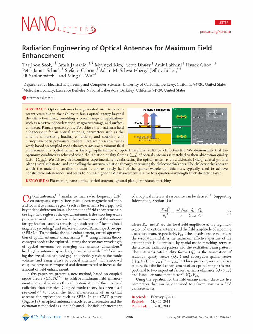
In this paper, we present a new method, based on coupledmode theory (CMT),12,13 to achieve maximum field enhance-ment in optical antennas through optimization of the antennas’radiation characteristics. Coupled mode theory has been usedpreviously13 to model the field enhancement of an opticalantenna for applications such as SERS. In the CMT picture(Figure 1a), an optical antenna is modeled as a resonator and theexcitation is modeled as a input channel. The field enhancement
of an optical antenna at resonance can be derived13 (SupportingInformation, Section I) as
jElocj2jEij2
¼ 2Acλresπ
QQ rad
QVeff
ð1Þ
where Eloc and Ei are the local field amplitude at the high fieldregion of an optical antenna and the field amplitude of incomingexcitation beam, respectively, Veff is the effective mode volume ofthe resonator, and Ac is the maximum effective aperture of theantenna that is determined by spatial mode matching betweenthe antenna radiation pattern and the excitation beam pattern.The antenna’s total quality factor (Q ) is the summation ofradiation quality factor (Qrad) and absorption quality factor(Q abs):Q
�1 =Q rad�1þQ abs
�1. This equation gives an intuitivepicture that the field enhancement of an optical antenna is pro-portional to two important factors: antenna efficiency (Q /Q rad)and Purcell enhancement factor19 (Q /Veff).
Using the equation for the field enhancement, there are fiveparameters that can be optimized to achieve maximum fieldenhancement:
Received: February 3, 2011Revised: May 11, 2011
ABSTRACT:Optical antennas have generatedmuch interest inrecent years due to their ability to focus optical energy beyondthe diffraction limit, benefiting a broad range of applicationssuch as sensitive photodetection, magnetic storage, and surface-enhanced Raman spectroscopy. To achieve the maximum fieldenhancement for an optical antenna, parameters such as theantenna dimensions, loading conditions, and coupling effi-ciency have been previously studied. Here, we present a frame-work, based on coupled-mode theory, to achievemaximum fieldenhancement in optical antennas through optimization of optical antennas’ radiation characteristics. We demonstrate that theoptimum condition is achieved when the radiation quality factor (Q rad) of optical antennas is matched to their absorption qualityfactor (Q abs). We achieve this condition experimentally by fabricating the optical antennas on a dielectric (SiO2) coated groundplane (metal substrate) and controlling the antenna radiation through optimizing the dielectric thickness. The dielectric thickness atwhich the matching condition occurs is approximately half of the quarter-wavelength thickness, typically used to achieveconstructive interference, and leads to ∼20% higher field enhancement relative to a quarter-wavelength thick dielectric layer.
KEYWORDS: Plasmonics, nano-optics, optical antenna, ground plane, impedance matching
2607 dx.doi.org/10.1021/nl2010862 |Nano Lett. 2011, 11, 2606–2610
Nano Letters LETTER
1 The antenna needs to be excited on resonance (λres),16
which can be achieved by tuning the antenna dimensions8
or loading the antenna gap with appropriate materials.9,14
2 The effective mode volume of the antenna (Veff) needs to bereduced, which can be achieved by shrinking the size ofantenna feed gap.2,20
3 Themaximum effective aperture (Ac) needs to be optimizedthrough matching the antenna’s radiation pattern with theexcitation signal.21 For example, the radiation pattern can beoptimized to match plane wave excitation using an antennaarray since the effective aperture is proportional to thedirectivity of the antenna and the directivity can be in-creased by the array factor.22
4 Another parameter that has not yet been explored andwhich we will discuss in this work is the optimum conditionfor an antenna’s relevant loss rates (i.e., Q , Q rad, Q abs). To
find the optimum, we take the derivative of eq 1 with respecttoQ rad and equate it to 0 (Supporting Information, SectionII). Since the effective aperture (Ac), effective mode volume(Veff), and the Q abs vary slowly compared to Q rad (seeSection III in Supporting Information and Figure 2c), themaximum field enhancement condition is achieved whenQ rad becomes equal to Q abs
Q rad ¼ Q abs ð2ÞThis is analogous to the impedance matching concept inantenna theory.23�25
5 At the optimum Q condition (Q rad = Q abs= 2Q ), theexpression for the field enhancement reduces to
jElocj2jEij2
¼ Acλ
π
QVef f
¼ Acλ
2πQabs
Vef fð3Þ
Therefore, the optimized field enhancement for givenmaterial is directly proportional to absorption quality factor(Q abs), which is a direct evidence of previously reported21
high field enhancementwith low loss material (such as silver).From the above recipe to achieve maximum field enhancement
for optical antennas, items 1, 2, 3, and 5 have previously been demon-strated. Here, we will introduce the concept of Q-matching foroptical antennas (item 4) and achieve the optimum conditionthrough radiation engineering. As the starting point, we will studythe radiation characteristics of a typical optical antenna fabricated ona glass substrate. To estimate the amount ofmismatch betweenQ rad
and Q abs for a gold dipole antenna (with 260 nm length, 40 nmwidth, 25 nm thickness, and 15 nm gap) on a quartz glass substrate,we have used time domain simulations based on finite integratetechnique (CSTMicrowave Studio) to calculateQ ,Q rad, andQ abs.
Figure 1. (a) Schematic and modeling of a dipole antenna as aresonator using the coupled mode theory (CMT). (b) Simulation of adipole antenna on a quartz glass. Most of the radiation from the antennais lost to the substrate resulting in a poor coupling from the plane waveexcitation to the antenna.
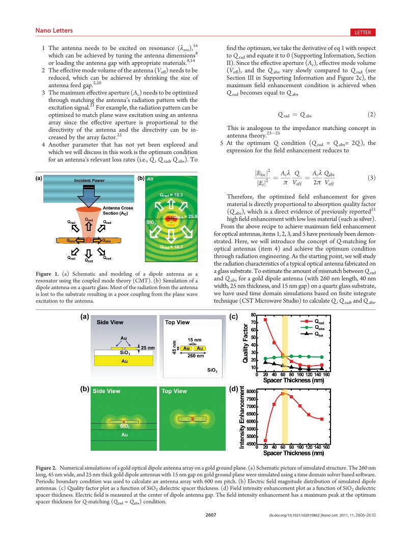
Figure 2. Numerical simulations of a gold optical dipole antenna array on a gold ground plane. (a) Schematic picture of simulated structure. The 260 nmlong, 45 nmwide, and 25 nm thick gold dipole antennas with 15 nm gap on gold ground plane were simulated using a time domain solver based software.Periodic boundary condition was used to calculate an antenna array with 600 nm pitch. (b) Electric field magnitude distribution of simulated dipoleantennas. (c) Quality factor plot as a function of SiO2 dielectric spacer thickness. (d) Field intensity enhancement plot as a function of SiO2 dielectricspacer thickness. Electric field is measured at the center of dipole antenna gap. The field intensity enhancement has a maximum peak at the optimumspacer thickness for Q-matching (Qrad = Qabs) condition.

2608 dx.doi.org/10.1021/nl2010862 |Nano Lett. 2011, 11, 2606–2610
Nano Letters LETTER
The total quality factor of the antenna (Q ) and the radiationQ ofthe antenna are calculated to be Q = 10.7 and Q rad = 18.3, re-spectively. The total quality factor of the antenna, Q, consists ofthe radiation (Q rad) and absorption (Q abs),Q
�1 =Q abs�1þQ rad
�1.Therefore, the absorption Q of the antenna can be calculated asQ abs
�1=Q�1�Q rad�1=10.7�1� 18.3�1=25.8�1.Thismismatch
between the radiationQ and absorptionQ reduces the energy coupl-ing into optical antennas, leading to smaller field enhancements.
To improve the antenna efficiency through Q matching, weneed to controllably tune either the radiation Q or absorptionQ of the antenna. Since absorptionQ of the antenna is dictated bythe metal loss (gold or silver), the radiation Q of the antennaneeds to be tuned. We achieve this radiation engineering ofoptical antennas using dielectric spacer coated metal groundplanes (Figure 2a). Metallic ground planes have been usedpreviously to enhance the fluorescence or SERS of moleculesplaced a distance of quarter-wavelength (λ/4) away from theground plane using a dielectric spacer.17,18 The λ/4 distanceresults in constructive interference between the top and bottomreflected emissions of the molecule and increases the effectiveaperture Ac. However, in addition to reflecting the bottomradiation, the ground plane can be used to control the radiationQ of the antenna and tune it to match the absorption Q ofantenna. For example, as the dielectric spacer thickness isreduced beyond the quarter-wavelength (λ/4) thickness, theantenna dipole and the antenna image dipole radiation canceleach other more and more. Therefore, as the dielectric spacerthickness is reduced, the radiation Q of the antenna is increasedand at the optimum dielectric spacer thickness, the radiation andabsorption Q of the antenna would be matched, which leads tothe maximum field enhancement condition.
We have used numerical simulation to verify this idea for agold dipole antenna array on dielectric (SiO2) coated goldground plane as shown in Figure 2a. Gold dipole antenna arrayswith 260 nm length, 40 nm width, 25 nm thickness, 15 nm gap,and 600 nm pitch were simulated using a finite integrationtechnique based software (CST Microwave Studio). The dipoleantenna array is excited by a plane wave from the top that ispolarized along the dipole antenna’s long axis. As indicated inFigure 2b, the electric field is mainly confined at the antenna feedgap on resonance. The total Q, radiation Q, and absorption Q ofthe antenna array are calculated as the thickness of SiO2 spacer layeris varied from 20 to 150 nm. As shown in Figure 2c, the radiationQincreases as the thickness of spacer decreases, which is expectedfrom the radiation cancellation between the real and the imagedipole antenna. The radiation Qmatches with the absorption Q atthe spacer layer thickness of 60 nm. The field intensity enhance-ment is also maximized at this optimum spacer thickness (60 nm),which agrees well with our theory (Figure 2d). It is important tonote that the optimum dielectric spacer thickness (60 nm) is lessthan half of the quarter-wavelength thickness of 150 nm.
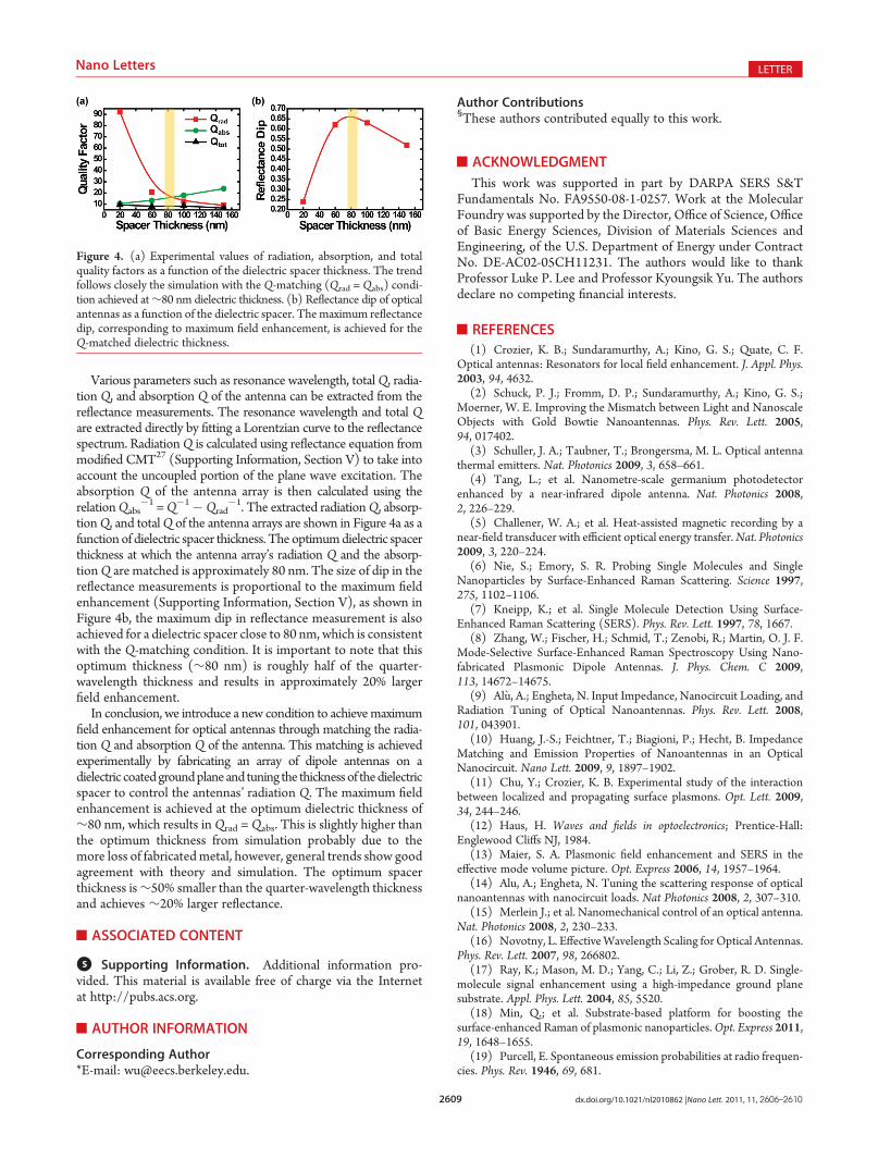
To experimentally verify the Q-matching condition, goldoptical dipole antenna arrays were fabricated on SiO2 spacercoated gold ground planes using high resolution e-beam litho-graphy and a lift-off process. For the ground plane, a 100 nm thickgold layer was evaporated on a Si wafer, and SiO2 layers of variousthicknesses (20, 60, 100, and 150 nm) were deposited usingplasma-enhanced chemical vapor deposition (PECVD). Wepatterned 260 nm long and 45 nm wide optical dipole antennasusing e-beam lithography followed by evaporation of 3 nm thickgermanium and 25 nm thick gold. Germanium adhesion layersreduce the roughness of gold surface26 (Supporting Information,
Section IV). The total size of the optical antenna array field is300μm� 300 μmand identical dipole antennas were distributedwith a 600 nm pitch (square array). Figure 3a shows the SEMpicture of fabricated optical dipole antenna array and the typicaldimensions of a single antenna are shown in the inset. Eachantenna has a length of 260 nm, width of 45 nm, and gap of15 nm. We use reflectance measurements to characterize theoptical antennas and the effect ofQ-matching since this measure-ment method is less sensitive to variations in parameters such asgap spacing caused by nonuniformities in e-beam lithographyexposure. The illumination from a halogen lamp was focused onthe antenna array using a 5�, NA = 0.13 objective lens and thereflection from the antenna array was collected through the sameobjective lens and sent to the spectrometer using a multicoreoptical fiber (Figure 3b). Figure 3c shows the normalized reflec-tion spectrum (reflectance) of the antenna arrays for variousdielectric spacer thicknesses, each spectrum is calculated bydividing the reflection from the antenna arrays with the reflectionfrom an area on the dielectric coated ground plane without anyantennas. Reflectance spectra show twomajor dips for each array.The larger dip position at longer wavelength corresponds to theantenna resonance and smaller dip corresponds to surface plasmonresonance supported by the periodic array.
Figure 3. Characterization of the fabricated optical antennas. (a) SEMimage of fabricated gold antenna arrays on a dielectric (SiO2) coated goldground plane. The inset shows a typical dipole antenna with 260 nm length,45 nm width, and 15 nm gap. (b) The reflection measurement setup forcharacterization of dipole antennas. (c) Normalized reflection (reflectance)spectra of the dipole antenna arrays for various dielectric (SiO2) thicknesses.The 100 nm SiO2 thickness displays the largest reflection dip, correspond-ing to strongest field enhancement as predicted by the theory. Reflectancespectra show twomajor dips for each array. The larger dip position at longerwavelength corresponds to the antenna resonance and smaller dip corre-sponds to surface plasmon resonance supported by the periodic array.
2609 dx.doi.org/10.1021/nl2010862 |Nano Lett. 2011, 11, 2606–2610
Nano Letters LETTER
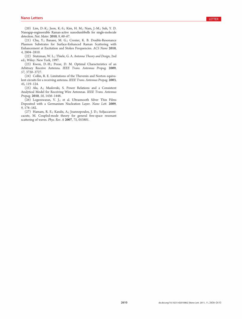
Various parameters such as resonance wavelength, totalQ, radia-tion Q, and absorption Q of the antenna can be extracted from thereflectance measurements. The resonance wavelength and total Qare extracted directly by fitting a Lorentzian curve to the reflectancespectrum. RadiationQ is calculated using reflectance equation frommodified CMT27 (Supporting Information, Section V) to take intoaccount the uncoupled portion of the plane wave excitation. Theabsorption Q of the antenna array is then calculated using therelationQabs
�1 =Q�1�Qrad�1. The extracted radiationQ, absorp-
tionQ, and totalQ of the antenna arrays are shown in Figure 4a as afunction of dielectric spacer thickness. The optimumdielectric spacerthickness at which the antenna array’s radiation Q and the absorp-tionQ are matched is approximately 80 nm. The size of dip in thereflectance measurements is proportional to the maximum fieldenhancement (Supporting Information, Section V), as shown inFigure 4b, the maximum dip in reflectance measurement is alsoachieved for a dielectric spacer close to 80 nm, which is consistentwith the Q-matching condition. It is important to note that thisoptimum thickness (∼80 nm) is roughly half of the quarter-wavelength thickness and results in approximately 20% largerfield enhancement.
In conclusion, we introduce a new condition to achievemaximumfield enhancement for optical antennas through matching the radia-tion Q and absorption Q of the antenna. This matching is achievedexperimentally by fabricating an array of dipole antennas on adielectric coatedgroundplane and tuning the thickness of thedielectricspacer to control the antennas’ radiation Q. The maximum fieldenhancement is achieved at the optimum dielectric thickness of∼80 nm, which results inQrad =Qabs. This is slightly higher thanthe optimum thickness from simulation probably due to themore loss of fabricatedmetal, however, general trends show goodagreement with theory and simulation. The optimum spacerthickness is∼50% smaller than the quarter-wavelength thicknessand achieves ∼20% larger reflectance.
’ASSOCIATED CONTENT
bS Supporting Information. Additional information pro-vided. This material is available free of charge via the Internetat http://pubs.acs.org.
’AUTHOR INFORMATION
Corresponding Author*E-mail: [email protected].
Author Contributions§These authors contributed equally to this work.
’ACKNOWLEDGMENT
This work was supported in part by DARPA SERS S&TFundamentals No. FA9550-08-1-0257. Work at the MolecularFoundry was supported by the Director, Office of Science, Officeof Basic Energy Sciences, Division of Materials Sciences andEngineering, of the U.S. Department of Energy under ContractNo. DE-AC02-05CH11231. The authors would like to thankProfessor Luke P. Lee and Professor Kyoungsik Yu. The authorsdeclare no competing financial interests.
’REFERENCES
(1) Crozier, K. B.; Sundaramurthy, A.; Kino, G. S.; Quate, C. F.Optical antennas: Resonators for local field enhancement. J. Appl. Phys.2003, 94, 4632.
(2) Schuck, P. J.; Fromm, D. P.; Sundaramurthy, A.; Kino, G. S.;Moerner, W. E. Improving the Mismatch between Light and NanoscaleObjects with Gold Bowtie Nanoantennas. Phys. Rev. Lett. 2005,94, 017402.
(3) Schuller, J. A.; Taubner, T.; Brongersma, M. L. Optical antennathermal emitters. Nat. Photonics 2009, 3, 658–661.
(4) Tang, L.; et al. Nanometre-scale germanium photodetectorenhanced by a near-infrared dipole antenna. Nat. Photonics 2008,2, 226–229.
(5) Challener, W. A.; et al. Heat-assisted magnetic recording by anear-field transducer with efficient optical energy transfer.Nat. Photonics2009, 3, 220–224.
(6) Nie, S.; Emory, S. R. Probing Single Molecules and SingleNanoparticles by Surface-Enhanced Raman Scattering. Science 1997,275, 1102–1106.
(7) Kneipp, K.; et al. Single Molecule Detection Using Surface-Enhanced Raman Scattering (SERS). Phys. Rev. Lett. 1997, 78, 1667.
(8) Zhang, W.; Fischer, H.; Schmid, T.; Zenobi, R.; Martin, O. J. F.Mode-Selective Surface-Enhanced Raman Spectroscopy Using Nano-fabricated Plasmonic Dipole Antennas. J. Phys. Chem. C 2009,113, 14672–14675.
(9) Al�u, A.; Engheta, N. Input Impedance, Nanocircuit Loading, andRadiation Tuning of Optical Nanoantennas. Phys. Rev. Lett. 2008,101, 043901.
(10) Huang, J.-S.; Feichtner, T.; Biagioni, P.; Hecht, B. ImpedanceMatching and Emission Properties of Nanoantennas in an OpticalNanocircuit. Nano Lett. 2009, 9, 1897–1902.
(11) Chu, Y.; Crozier, K. B. Experimental study of the interactionbetween localized and propagating surface plasmons. Opt. Lett. 2009,34, 244–246.
(12) Haus, H. Waves and fields in optoelectronics; Prentice-Hall:Englewood Cliffs NJ, 1984.
(13) Maier, S. A. Plasmonic field enhancement and SERS in theeffective mode volume picture. Opt. Express 2006, 14, 1957–1964.
(14) Alu, A.; Engheta, N. Tuning the scattering response of opticalnanoantennas with nanocircuit loads. Nat Photonics 2008, 2, 307–310.
(15) Merlein J.; et al. Nanomechanical control of an optical antenna.Nat. Photonics 2008, 2, 230–233.
(16) Novotny, L. EffectiveWavelength Scaling for Optical Antennas.Phys. Rev. Lett. 2007, 98, 266802.
(17) Ray, K.; Mason, M. D.; Yang, C.; Li, Z.; Grober, R. D. Single-molecule signal enhancement using a high-impedance ground planesubstrate. Appl. Phys. Lett. 2004, 85, 5520.
(18) Min, Q.; et al. Substrate-based platform for boosting thesurface-enhanced Raman of plasmonic nanoparticles.Opt. Express 2011,19, 1648–1655.
(19) Purcell, E. Spontaneous emission probabilities at radio frequen-cies. Phys. Rev. 1946, 69, 681.
Figure 4. (a) Experimental values of radiation, absorption, and totalquality factors as a function of the dielectric spacer thickness. The trendfollows closely the simulation with the Q-matching (Qrad = Qabs) condi-tion achieved at∼80 nm dielectric thickness. (b) Reflectance dip of opticalantennas as a function of the dielectric spacer. The maximum reflectancedip, corresponding to maximum field enhancement, is achieved for theQ-matched dielectric thickness.
2610 dx.doi.org/10.1021/nl2010862 |Nano Lett. 2011, 11, 2606–2610
Nano Letters LETTER
(20) Lim, D.-K.; Jeon, K.-S.; Kim, H. M.; Nam, J.-M.; Suh, Y. D.Nanogap-engineerable Raman-active nanodumbbells for single-moleculedetection. Nat. Mater. 2010, 9, 60–67.(21) Chu, Y.; Banaee, M. G.; Crozier, K. B. Double-Resonance
Plasmon Substrates for Surface-Enhanced Raman Scattering withEnhancement at Excitation and Stokes Frequencies. ACS Nano 2010,4, 2804–2810.(22) Stutzman, W. L.; Thiele, G. A. Antenna Theory and Design, 2nd
ed.; Wiley: New York, 1997.(23) Kwon, D.-H.; Pozar, D. M. Optimal Characteristics of an
Arbitrary Receive Antenna. IEEE Trans. Antennas Propag. 2009,57, 3720–3727.(24) Collin, R. E. Limitations of the Thevenin and Norton equiva-
lent circuits for a receiving antenna. IEEE Trans. Antennas Propag. 2003,45, 119–124.(25) Alu, A.; Maslovski, S. Power Relations and a Consistent
Analytical Model for Receiving Wire Antennas. IEEE Trans. AntennasPropag. 2010, 58, 1436–1448.(26) Logeeswaran, V. J.; et al. Ultrasmooth Silver Thin Films
Deposited with a Germanium Nucleation Layer. Nano Lett. 2009,9, 178–182.(27) Hamam, R. E.; Karalis, A.; Joannopoulos, J. D.; Soljaccaroni-
cacute, M. Coupled-mode theory for general free-space resonantscattering of waves. Phys. Rev. A 2007, 75, 053801.