radiation-tolerant proasic3 fpgas radiation effects - microsemi
TRANSCRIPT

Radiation-TolerantProASIC3 FPGAsRadiation Effects
April 2010April 2010

Table of Contents
2 Radiation-Tolerant ProASIC3 FPGAs Radiation Effects
Introduction . . . . . . . . . . . . . . . . . . . . . . . . . . . . . . . . . . . . . . . . . . . . . . . . . . . . . . . . . 3New Radiation-Tolerant 0.13-µm Flash-FPGAs . . . . . . . . . . . . . . . . . . . . . . . . . . . . 4
ProASIC3 Internal Architecture . . . . . . . . . . . . . . . . . . . . . . . . . . . . . . . . . . . . . . . . . . . . . . . . . . . . . . . 4Floating Gate Device . . . . . . . . . . . . . . . . . . . . . . . . . . . . . . . . . . . . . . . . . . . . . . . . . . . . . . . . . . . . . . 5ProASIC3E and Low-Power ProASIC3EL . . . . . . . . . . . . . . . . . . . . . . . . . . . . . . . . . . . . . . . . . . . . . . 5
TID Characterization . . . . . . . . . . . . . . . . . . . . . . . . . . . . . . . . . . . . . . . . . . . . . . . . . . 6TID Effects on Floating Gate Transistors . . . . . . . . . . . . . . . . . . . . . . . . . . . . . . . . . . . . . . . . . . . . . . . 6TID Performance of the FPGA Core . . . . . . . . . . . . . . . . . . . . . . . . . . . . . . . . . . . . . . . . . . . . . . . . . . . 7
Test Design and Test Procedure . . . . . . . . . . . . . . . . . . . . . . . . . . . . . . . . . . . . . . . . . . . . . . . . . . . 7X-Ray Test Results . . . . . . . . . . . . . . . . . . . . . . . . . . . . . . . . . . . . . . . . . . . . . . . . . . . . . . . . . . . . . 8Gamma Rays Test Results . . . . . . . . . . . . . . . . . . . . . . . . . . . . . . . . . . . . . . . . . . . . . . . . . . . . . . 10
TID Performance of the Programming Control Circuit . . . . . . . . . . . . . . . . . . . . . . . . . . . . . . . . . . . . 11FG Refreshing and Annealing Effects on the Product’s TID Limit . . . . . . . . . . . . . . . . . . . . . . . . . . . 12
Test Procedure . . . . . . . . . . . . . . . . . . . . . . . . . . . . . . . . . . . . . . . . . . . . . . . . . . . . . . . . . . . . . . . 12Test Results of the Refreshing Effects . . . . . . . . . . . . . . . . . . . . . . . . . . . . . . . . . . . . . . . . . . . . . 12
SEE Characterization . . . . . . . . . . . . . . . . . . . . . . . . . . . . . . . . . . . . . . . . . . . . . . . . . 14Devices Under Test and Experimental Test Setup . . . . . . . . . . . . . . . . . . . . . . . . . . . . . . . . . . . . . . . 14Test Designs and Experimental Results . . . . . . . . . . . . . . . . . . . . . . . . . . . . . . . . . . . . . . . . . . . . . . . 16
FPGA Core SEE Characterization (Flip-Flops) . . . . . . . . . . . . . . . . . . . . . . . . . . . . . . . . . . . . . . . 16PLL SEE Characterization . . . . . . . . . . . . . . . . . . . . . . . . . . . . . . . . . . . . . . . . . . . . . . . . . . . . . . . 20FlashROM (FROM) Memory SEE Characterization . . . . . . . . . . . . . . . . . . . . . . . . . . . . . . . . . . . 22SRAM Memory SEE Characterization . . . . . . . . . . . . . . . . . . . . . . . . . . . . . . . . . . . . . . . . . . . . . . 23
Preliminary Studies of TID Effects on SEE Sensitivities . . . . . . . . . . . . . . . . . . . . 26Proton Characterization of the Programming and Erase Circuitry . . . . . . . . . . . . . . . . . . . . . . . . . . . 26Testing Beyond the TID Limit . . . . . . . . . . . . . . . . . . . . . . . . . . . . . . . . . . . . . . . . . . . . . . . . . . . . . . . 27
Conclusion . . . . . . . . . . . . . . . . . . . . . . . . . . . . . . . . . . . . . . . . . . . . . . . . . . . . . . . . . 28Acknowledgements . . . . . . . . . . . . . . . . . . . . . . . . . . . . . . . . . . . . . . . . . . . . . . . . . . 29References . . . . . . . . . . . . . . . . . . . . . . . . . . . . . . . . . . . . . . . . . . . . . . . . . . . . . . . . . 29

Radiation-Tolerant ProASIC3 FPGAs Radiation Effects
IntroductionNonvolatile and reconfigurable field programmable gate arrays (FPGAs) present an attractive solution for high-level system integration in various aerospace and military applications. Commercially available low power flash-based FPGAs, 0.13-µm ProASIC3®/L and its extended family product (ProASIC3EL) are nonvolatile and provide remote in-system reprogramming to support future design iterations and field upgrades. Flash-based technology provides the advantage of being a secure, low power, single-chip solution [Morris, 2006]. Unlike SRAM based-FPGAs, the configuration memories are not volatile and hence do not require additional nonvolatile memory to reload the device configuration data at system-power-up or due to radiation effects [Swift et al., 2004]. The entire set of configuration bits has triple module redundancy (TMR) [Carmichael, 2001]. This reduces cost, power, and initialization time and improves system reliability. However, despite the SEE immunity of their ProASIC3/L configuration memory, floating gate (FG) switches and CMOS logic gates are susceptible to total ionizing dose (TID) effects and single-event effects (SEE).For TID effects, the primary issue is the radiation-induced charge loss in the floating gate [Snyder et al., 1989, Cellere et al., 2004, Wang et al., 2004, Guertin et al., 2006], resulting in a change in FPGA electrical performance (maximum speed, current, etc.). For SEE, the primary concern resides in the upset of its registers (state of the flip-flop) due to a particle hit, resulting in disruption of the normal operation of the FPGA-design [Rezgui et al., 2007, 2008a and 2008b]. The new radiation-tolerant ProASIC3 family (RT ProASIC3), sharing the same silicon as the low power ProASIC3L FPGAs, is hardened for TID and SEE by software means in a manner transparent to the user [Rezgui et al., 2008a]. Single-event transients (SET) tolerance is hardened by single or duplication filtering [Shuler et al., 2005 and 2006, Balasubramanian et al., 2005, Baze et al., 2006, Mavis and Eaton, 2007, Rezgui et al., 2007a] and single-event upsets (SEU) tolerance is hardened by TMR or error detection and correction (EDAC) to soft error rates of less than 10-10 upsets/bit-day and LETth larger than 40 MeV•cm2/mg for clock frequency up to 100 MHz. The TID limit is improved by simple reprogramming of the FPGA, resulting in the restoration of the charge loss from their configuration FG switches.This report describes the employed mitigation techniques for the ProASIC3 product family to attain the radiation levels of the radiation-tolerant product and presents the results obtained from the TID and SEE characterization of ProASIC3 and ProASIC3L (the low power version of ProASIC3) devices. The SET characterization or mitigation is not addressed in this report, but detailed analyses and measurements of SET cross-sections are provided in [Rezgui et al., 2007, 2008a, 2008b and 2009]. This chapter includes a brief description of the RT ProASIC3 FPGA from architectural and device perspectives as well as detailed analyses of the radiation test results issued from 1) the TID characterization, 2) the SEE characterization and 3) the TID effects on the SEE sensitivities.
April 2010

New Radiation-Tolerant 0.13-µm Flash-FPGAsBased on its low power capabilities and its increased I/O features in the extended (E) family product, the 0.13-µm ProASIC3EL part is selected as the silicon foundation of the new radiation-tolerant flash-based FPGA (RT ProASIC3). Additionally, RT ProASIC3 FPGAs are assembled in hermetically-sealed ceramic packages, which are available as Column Grid Array (CG, with Six Sigma solder columns attached), Land Grid Array (LG, no solder columns attached), or Ceramic Quad Flat-Pack (CQFP). Qualification, inspection, assembly, and testing are performed in accordance with MIL-STD-883 Class B [MIL-STD-883G]. In the following sections, a brief description of these products at the architectural and the device levels is given, as well as an explanation of the differences between ProASIC3 and ProASIC3L product families.
ProASIC3 Internal ArchitectureThe ProASIC3EL product family has up to 3 million system gates, 504 Kbits of true dual-port SRAM, 620 single-ended I/Os, and 300 differential I/O pairs. ProASIC3EL devices also include 1 Kbit of on-chip, programmable, nonvolatile FlashROM (FROM) memory storage as well as up to 6 integrated phase-locked loops (PLL). The FPGA core consists of logic tiles, called VersaTiles, and routing structures. Each logic tile is a combination of CMOS logic and flash switches and can be configured as a three-input logic function, a D-flip-flop with an optional enable, or a latch by programming the appropriate flash switch interconnections. The logic tiles are connected with each other through routing structures and FG switches. These flash switches are distributed throughout the device to provide reconfigurable programming to connect signal lines to the appropriate logic-tile inputs and outputs [ProAISC3 Handbook], as shown in Figure 1. Flash FPGAs are reprogrammable through the JTAG port and contain programming control circuits composed of charge pumps, sense amplifiers, digital-to-analog converters (DAC), CMOS logic, high voltage (HV) NMOS transistors, and FG cells to store the factory parameters.
Each logic tile is a combination of CMOS logic and flash switches.
Figure 1: ProASIC3 FPGA Core, VersaTile (Logic Tile), and Flash-Based Switch
4 Radiation-Tolerant ProASIC3 FPGAs Radiation Effects

Floating Gate DeviceAs shown in Figure 1 on page 4 and detailed in [Wang et al., 2004a, 2006a and 2006b], the FPGA switch circuit is a set of two NMOS transistors: 1) a sense transistor to program the floating gate and sense the current during the threshold voltage measurement and 2) a switch transistor to turn ON or OFF a data-path in the FPGA. The two transistors share the same control gate and floating gate. The threshold voltage is determined by the stored charge in the FG. Fowler-Nordheim tunneling through the thin gate oxide (100 A) is the mechanism that modulates the stored charge during program and erase of the FG. The FG switch is programmed to a low threshold voltage state to turn the switch ON and erased to a high threshold voltage state to turn it OFF. Figure 2 shows the structure of the FG transistor: an NMOS transistor with a stacked gate. Between the silicon substrate and the floating gate is the tunnel oxide and between the FG and the control gate is inter-poly oxide-nitride-oxide (ONO) composite dielectric.
The floating gate transistor in the flash-based FPGA is a set of two NMOS transistors: 1) a sense transistor to program the floating gate and sense the current during the threshold voltage measurement and 2) a switch transistor to turn ON or OFF a data-path in the FPGA.
ProASIC3E and Low-Power ProASIC3ELThe low power ProASIC3L and ProASIC3EL parts are processed at UMC, whereas ProASIC3 and ProASIC3E parts may be processed at either UMC or Infineon. ProASIC3L and ProASIC3EL parts are identical at the design and architectural levels and are pin-to-pin compatible with the ProASIC3 and ProASIC3E parts, except that the L parts possess a new added feature called Flash*Freeze.™ This feature provides a low power static mode that retains all SRAM and register information with rapid recovery to active (operating) mode, by simply asserting a single input. The device then enters a low power mode in one microsecond, in which clocks are frozen, I/Os are tristated, and core registers and memories maintain state. In this mode, external signals driving the FPGA I/Os and clocks can still be toggled without impact on the device power consumption. For instance, in Flash*Freeze mode, the power consumption of the low power FPGAs ranges in the tens of microwatts [ProASIC3 Handbook].Furthermore, and because of their basic process differences, resulting mainly in the increase of their threshold voltages, the ProASIC3EL products have much lower power consumption than the ProASIC3E parts. For instance, a ProASIC3EL FPGA operates at 40 percent lower dynamic power and 90 percent lower static power than the ProASIC3E FPGAs, and orders of magnitude lower power than the SRAM-based FPGAs, with up to 350 MHz operation. These process differences between the two product families (ProASIC3E and ProASIC3EL) are only induced in the CMOS transistors used to build the FPGA logic blocks but not in the FG transistors. Since TID has less effect on the CMOS transistors than on the FG
Figure 2: Floating Gate Transistor
Radiation-Tolerant ProASIC3 FPGAs Radiation Effects 5

transistors, the same TID performance should be expected for both of the ProASIC3E and ProASIC3EL parts when both are operated at 1.5 V core voltage. In addition, the ProASIC3EL can operate at all core voltages between 1.2 V and 1.5 V, which allows more reduction in their power consumption when operated at 1.2 V. In the following sections, the test results issued from TID and SEE test experiments of ProASIC3 devices are reported and discussed along with additional suggestions on mitigation methodologies suitable for the target device. For these experiments, a few devices were selected for the TID characterization in x-rays and gamma rays (A3P250 and A3PL600) and the SEE characterization in heavy-ions (HI) and protons beams (the A3P250 and the A3P1000). Since ProASIC3/E and ProASIC3L/EL devices share the same FPGA core, the radiation test results are expected to be very similar.
TID CharacterizationThis section covers the TID performance at the product level of the ProASIC3 and the low power RT ProASIC3 product families. Radiation tests for the selected products were performed with x-rays at ARACOR facility, in Sunnyvale, CA and with gamma rays at the Defense MicroElectronics Activity (DMEA), in Sacramento, CA. The x-ray irradiation tests were performed by an ARACOR 4100 x-ray irradiator. The TID test results are reported and discussed, along with additional suggestions for extending the TID lifetime of flash FPGAs.The purpose of this characterization is to study the TID effects on 1) the FPGA core (CMOS logic and FG devices) and 2) the programming control circuit (FG devices, charge pumps, analog circuits, and HV NMOS devices). TID irradiation tests for the selected features were performed with x-rays and gamma rays. Most of the results presented in this chapter are obtained with x-rays beams whose effects are estimated to be approximately 2.9 times less effective than those measured in gamma rays [Wang et al., 2004]. This calibration factor between the x-rays and the gamma ray data was calculated experimentally using the same methodology previously applied in [Palkuti and LePage, 1982]. Additionally, all the x-ray irradiation tests were performed on the ProASIC3 parts (A3P250-PQ208) while gamma test experiments at DMEA, were performed on the ProASIC3L part (A3P600L-FG484), both when operated at 1.5 V core voltage. During all x-ray and gamma dose irradiations, except for the power pins, all the device under-test (DUT) inputs are grounded; the ambient is at room temperature.
TID Effects on Floating Gate TransistorsThree radiation-induced mechanisms detailed in [Wang et al., 2004, Brown and Brewer, 2002] can affect the threshold voltage of the FG devices: 1) holes injected into the FG, 2) holes trapped in the oxides and 3) electrons emitted over the polysilicon/oxide barriers. Electron-hole pairs initiated by the radiation test result in the injection of holes in the FG and the trapping of holes in the oxides. Hole injection and trapping have a similar effect, since they both reduce the threshold voltage in the FG device. The third radiation phenomenon, electron emission, occurs mainly when radiation-induced photons possess an energy exceeding the potential barrier. The emitted electrons are then swept to the substrate or control gate by the
6 Radiation-Tolerant ProASIC3 FPGAs Radiation Effects

electric field, which reduces the FG threshold voltage. Figure 3 shows an example of threshold voltage (Vt) shift in both the program and erase distributions of the FG devices when irradiated with x-rays.
The charge loss effects on the FG were investigated by x-ray irradiation in [4-7].The fundamental, consistent physical process of charge generation, separation, and trapping in the dielectrics surrounding the floating gate will modulate the threshold voltage (Vt) of the floating gate (FG) device and subsequently the function of the FPGA. The major key TID-indicating electrical parameters on a given FPGA design are 1) the propagation delay, which is best measured on an inverter-string design, and 2) the maximum allowed frequency of the circuit registers. In the following, TID-induced effects on a given design will be discussed for both of the DUTs mentioned above (ProASIC3 and ProASIC3L).
TID Performance of the FPGA CoreTest Design and Test ProcedureTo measure the TID effects on the FPGA core, three ProASIC3 FPGAs were configured with three sub-designs: D1) an inverter-string with 1,000 stages; D2) a shift register with 1,000 D-flip-flops (DFF) running at 350 MHz; and D3) a shift register with 310 DFFs combined with combinational logic (12 inverters) between each consecutive flip-flop running at 135 MHz. Before x-ray irradiation, at 0 Krad, both of the rising and falling edges of the D1 output signal are measured and on average are approximately 530 ns. The maximum attained frequency of the D2 design was 350 MHz, as stated in the [ProASIC3 Handbook], while the maximum frequency for D3 is about 135 MHz. For both of the D2 and the D3 test designs, the input data are toggling at half of the clock frequency and at the positive edge of the clock-input, while their output data are switching at the clock negative edge. After exposure to a certain dose, the rising and falling
Figure 3: Threshold Voltage Degradation vs. TID of X-Rays Irradiation for an A3P250-PQ208 DUT
Radiation-Tolerant ProASIC3 FPGAs Radiation Effects 7

edges for the D1 output signal and the maximum attained frequency for the D2 and the D3 sub-designs were measured. A block diagram of the DUT design is given in Figure 4.
This design is shared in three sub-designs: D1) an inverter-string; D2) a shift register; and D3) a shift register combined with combinational logic between each consecutive flip-flops.The input signals for each sub-design are supplied from an off-chip pulse generator while the electrical parameters of the three output signals were observed and recorded on the scope off-beam after two minutes from each DUT irradiation. The same tests applied to the ProASIC3 part, combining combinational and sequential logic, have been repeated in gamma rays for the A3PL600-FG484 FPGA at DMEA and the issued results are reported. The dose rate during these tests was varied between 4 and 25 Krad/min (67 and 461 rad/s), which is higher than the dose rate required by the TM1019.7 (50 rad/s) [MIL-STD-883G].
X-Ray Test ResultsThe test circuits were exposed continuously to TID until one of the three sub-design’s output state became unstable off beam and required annealing to recover normal operation. This instability in the output signals was always accompanied by an increase of the current in the FPGA core (from 1 to 33 mA in the worst observed case) and was mainly observed starting from an x-ray total dose of 175 Krad (equivalent to 60 Krad in gamma rays). The results obtained for the ProASIC3 FPGA, displayed in Figure 5 on page 9, show
Figure 4: Block Diagram of the DUT Design
8 Radiation-Tolerant ProASIC3 FPGAs Radiation Effects

that for the ProASIC3 parts (DUT 3), the 10% degradation in propagation delay was obtained at 66 Krad (equivalent to 22 Krad in gamma rays).
Furthermore, as shown in Figure 6, until a TID of 78 Krad, no differences in the maximum allowed frequency for the D2 was noticed, which means that all the DFFs can still operate at 350 MHz. This means that all the timing requirements (setup time, etc.) needed for the DFF were still valid. However, when combining both combinational and sequential logic in one single design (D3), the TID limit to observe a variation in the maximum frequency was reduced to 70 Krad, as shown in Figure 7 on page 10. Indeed, the true maximum frequency of a DFF is about 2 GHz, but because of the I/Os and internal FPGA routing, the effective maximum frequency is reduced to 350 MHz.
Figure 5: Per Cent Propagation-Delay Degradation vs. TID of X-Ray Irradiation for Three A3P250-PQ208 DUTs
Figure 6: Per Cent D2 Frequency Degradation vs. TID of X-Ray Irradiation for Three A3P250-PQ208 DUTs
Radiation-Tolerant ProASIC3 FPGAs Radiation Effects 9

Degradation in the D2 maximum frequency was observed only at 75 Krad. Degradation of 10% for the D1 was observed at 66 Krad, D2 (78 Krad), and D3 (70 Krad).
In the following sections, the same test data will be compared to gamma rays to calculate the circuits’ TID performance and verify the 2.9 factor between the x-rays and the gamma radiations.
Gamma Rays Test ResultsThe A3PL600-FG484 was exposed to gamma irradiation at the core voltage of 1.5 V. Figure 8 on page 11 shows the measured degradation in the propagation delay in the inverter-string along with the extrapolated data from the previously obtained data in x-ray irradiation (Figure 7) based on the 2.9 factor. The obtained results show that the measured and predicted TID limit correlate quite well, confirming the correctness of the 2.9 factor between the gamma and x-ray dose irradiations. However, as the only purpose of this comparison is the correlation between x-ray and the gamma ray radiation data, it is certainly not the objective to show which one has the higher TID effects. On the other hand, this data confirms that the TID limit of the ProASIC3L part is around 22 Krad relative to gamma rays. Additionally, and as shown in Figure 9 on page 11, the obtained data for the D2 show no degradation in the flip-flops maximum frequency until a TID of 28 Krad (the last tested value). This confirms the same x-rays test results, proving
Figure 7: Per Cent D1, D2, and D3 Electrical Parameters Degradation vs. TID of X-Rays Irradiation for Three A3P250-PQ208 DUTs
10 Radiation-Tolerant ProASIC3 FPGAs Radiation Effects

again that a degradation in the speed performances of a logic tile configured as a flip-flop is less observable than on a logic tile configured as an inverter.
For x-ray TID testing, however, the TID performance of D3, although slightly better (28 Krad), follows the trend of the TID performance of D1 (the inverter-string). This is expected, since D3 combines both sequential and combinational logic.
TID Performance of the Programming Control CircuitThe main function of this circuit is to erase, program, and measure the threshold voltages (Vt) of each sense FG device. As a consequence, the test flow consists of reprogramming the part, which invokes erasing, reprogramming, and verifying the correctness of the configured design by measuring the Vt of all the sense devices. For clarity purposes, the entire procedure will be called reprogramming or refreshing of the part. The test flow, applied on the ProASIC3 parts, consisted of reprogramming the part off-beam after its irradiation to a certain dose (10 Krad in x-rays in this case) until failure to reprogram was observed.
Figure 8: Per Cent Propagation Delay Degradation vs. TID of Gamma Ray Irradiation for A3P600-FG484 DUT with the Correlation Factor (2.9)
Figure 9: Per Cent D1, D2, and D3 Electrical Parameters Degradation vs. TID of X-Ray Irradiation for Three A3P250-PQ208 DUTs
Radiation-Tolerant ProASIC3 FPGAs Radiation Effects 11

The test results showed that the maximum TID at which the programming procedure passed was 40 Krad, since it failed at 50 Krad, which suggests that the TID limit of this sub-circuit is between 40 and 50 Krad in x-rays. Note that all the three tested parts that were exposed to 50 Krad recovered the reprogramming capability at room temperature after a few days. This means that this part is subject to annealing effects. The following section will show some of these effects. The TID limit in x-ray irradiation for the FPGA core was about 66 Krad, while for the programming control circuit, it is about 40 Krad. This difference in the TID limits could be due to the FG devices located in the programming control circuit, the thick-oxide HV devices, possibly the analog circuits or the charge pumps.
FG Refreshing and Annealing Effects on the Product’s TID LimitTest ProcedureAs explained in [Wang et al., 2004 and 2006], the percentage of the degradation in the propagation delay is mainly due to the charge loss in the FG devices (whether in the erase or the program state). Therefore, a first TID mitigation solution would be to attempt to restore that charge to these FG cells. This refresh could simply be done by erasing and reprogramming the flash FPGA. However, since the previous results showed that the programming circuit is limited to 40 Krad in x-ray irradiation, unless annealing effects are taken into account, the test flow consisted in reprogramming the part off-beam after having been irradiated to 10, 20, 30 and 40 Krad (x-rays). On the other hand, when starting from a much higher TID (85 Krad in x-rays), the measurements of the electrical parameters of D1, D2, and D3 became variable with time, requiring longer than 2 minutes to get a stable value of the output states. These electrical parameters improved with annealing time and were then recorded after 2, 15, and 30 minutes, starting from a TID of 85 Krad. Indeed, as shown in Figure 10, three data points are displayed at 85, 95, and 105 Krad. An improvement of 10% was observed between each measurement taken at 2, 15, and 30 minutes at these three TID values, clearly showing the annealing impact on the FG devices.
These effects are clearly observed for TID higher than 85 Krad.
Test Results of the Refreshing EffectsThe obtained results, shown in Figure 11, demonstrate clearly the efficacy of the employed refresh technique in restoring the charge lost from the FG devices. They also show that at each refresh, the three
Figure 10: Annealing Effects on the A3P250 DUTs. These effects are clearly observed for TID higher than 85 Krad
12 Radiation-Tolerant ProASIC3 FPGAs Radiation Effects

sub-designs restore completely the original operational parameters (rising and falling times as well the maximum frequencies). Indeed, the maximum TID limit (based on 10% degradation in the propagation delay) was increased by 18 Krad, improving it from 22 to 40 Krad (calculated for gamma radiation). This suggests that if the programming circuitry was more robust to TID effects, the overall TID lifetime of the FPGA core could be extended to higher than 40 Krad in gamma radiation. Note, that the predicted data shown in Figure 11 was extracted from the TID measurements during the DUT exposition to x-rays. Both the x-rays and gamma induced-radiation correlate again quite well and confirm the 2.9 factor. Furthermore, after each refresh cycle (10 Krad irradiation in x-rays), the threshold voltages were measured. The obtained Vt distributions, similar to what has been shown in Figure 3, prove that all the FG devices have regained their charge lost because of TID, and shifted back to their original Vt, whether they were initially in the program or erase state.Note that when employing the refresh techniques, the three sub-designs remained functional, proving that no switching of the FG transistors from ON to OFF and vice versa has occurred, until a TID of 275 Krad, in x-rays which should be equivalent to 95 Krad when exposed to gamma rays. Furthermore, since the three sub-designs use 99% of the FPGA logic tiles and remained fully functional, it is then clear that there are no stuck bits because of x-ray or gamma irradiation.
The reprogramming of the ProASIC3 part in gamma and x-rays restore the lost charge from the FG devices and increase the product’s TID limit.In summary, the obtained results showed TID sensitivity in the FPGA core and the programming control circuit of the FPGA. A degradation of 10% in the propagation delays was attained at 22 Krad and the part could not be reprogrammed after 16 Krad when exposed to gamma rays. However, two phenomena to mitigate the TID effects on the FG devices have been observed: 1) the considerable annealing effects and 2) the impact of the FPGA refreshing to restore the FG lost charge. Indeed, after each refresh of the FPGA core, the latter recovers the original electrical parameters, as if it has not been irradiated. Because of the low TID performance of the programming control circuit, the TID limit of the FPGA core could not be improved to higher than 40 Krad in gamma rays. In the next section, the SEE characterization and mitigation of the 0.13-µm ProASIC3 FPGAs will be addressed [Rezgui et al., 2007a, 2008b and 2009].
Figure 11: Refresh Effects on the A3P250 DUTs
Radiation-Tolerant ProASIC3 FPGAs Radiation Effects 13

SEE CharacterizationThe SEE characterization of the ProASIC3 FPGA was performed in heavy ion (HI) and proton beam experiments. HI beam experiments were performed at the facility of Texas A&M University (TAMU) and at the Lawrence Berkeley National Laboratories (LBNL). Proton radiation experiments were conducted at the Crocker Nuclear Laboratory of California in Davis (CNL). HI beam experiments were performed with a wide ion-cocktail (Neon, Argon, Copper, Krypton and Xenon) at normal incidences and two additional tilt angles (30° and 45°). No testing with rolling angles was performed, nor is differentiation in the data collected at normal incidence or tilt angles is provided in this chapter.Radiation tests targeted primarily the five elements of the ProASIC3 programmable architectures:
1. FPGA core2. Clock network and PLL3. FlashROM (nonvolatile memory)4. SRAM
Devices Under Test and Experimental Test SetupFor the beam test experiments, two devices from the ProASIC3 product family were selected: the A3P250 and the A3P1000. Each selected part is mounted in a PQ208 package. Table 1 shows the features of the two selected parts. The test primarily targets the circuitry used for the DUT erase and programming depicted on the bottom of Figure 1 on page 4 as the block for charge pumps, as well as the five configurable architectures in the ProASIC3 FPGA, also shown in Figure 1 on page 4: 1) the FPGA core, 2) the clock network and the PLL, 3) the FROM and 4) the SRAM.
A new test setup was built for the ProASIC3 radiation testing. As shown in Figure 12 on page 15, it includes two boards: 1) a master board for the monitoring and control of the DUT operation in-beam and 2) a slave board for communication between the host PC and the master board through two USB ports. The master board includes an A3P1000-FG484, called master FPGA, and a DUT (A3P-PQ208). I/O channels of an input (single-ended, SE or LVDS) routed immediately to a nearby output are also added between the master FPGA and the DUT. There are 38 SE and 13 LVDS I/O channels on both FPGAs. This board architecture allows the implementation of several separate designs on the same DUT to be tested
Table 1: Features of the Selected DUTs: A3P250 and the A3P1000, PQ208 PackagePart A3P250 A3P1000
System Gates 250K 1M
D-Flip-Flops 6,144 24,576
RAM Kbits 36 144
FlashROM 1K 1K
Secure (AES) ISP Yes Yes
Integrated PLL 1 1
Global Signals 18 18
I/O Banks 4 4
Single-Ended I/Os 151 154
Differential I/O Pairs 34 35
14 Radiation-Tolerant ProASIC3 FPGAs Radiation Effects

simultaneously. The slave board includes an A3P1000-PQ208; it allows the data acquisition and data transfer to the host PC.
For communication with the host PC, a generic user interface was designed to communicate with the slave board. The communication protocol between the slave board and the host PC remains always the same for easy and fast implementation of any new SEE test experiment. Indeed, there are a maximum of 64 display counters available to the designer, which can be labeled according to the running experiments. These counters are usually used for display of number of SEE events among other indicators of the operation of the DUT design. In addition, this user interface allows the self-monitoring of the test system itself, by testing each board and FPGA individually, as shown in the Mode knob on the top left of Figure 13 on page 16.
Figure 12: Block Diagram of the ProASIC3 Test Setup
Radiation-Tolerant ProASIC3 FPGAs Radiation Effects 15

Among other features, the interface also allows the pattern selection using the pattern knob (all zeroes, all ones, checkerboard, or inversion of checkerboard) exercised on the DUT inputs. The frequency at which the DUT design is running is controlled by using the Frequency knob.
Test Designs and Experimental ResultsFPGA Core SEE Characterization (Flip-Flops)The purpose of this testing is to determine the SEE cross-section of an ProASIC3 logic tile configured as a DFF. This should lead to the highest possible upset cross-section of a logic tile. The basic test design is a shift register (SR) using 86 logic tiles, with each one of them configured as a DFF and one global clock signal but no reset signal. Note that if the SR design was using a reset line, this signal would be a global and using a global I/O pad in the same way as any other global clock signal, whose cross-section will be given below.On the other hand, since this is a 0.13-µm technology, the part might be sensitive to multiple bit upsets (MBU) [Quinn et al., 2005], which in some cases cannot be mitigated effectively by TMR. For instance, if
Figure 13: SEE Software User Interface with a Maximum of 64 Display Counters
16 Radiation-Tolerant ProASIC3 FPGAs Radiation Effects

the MBU affects two TMR paths out of three, the output TMR result will be wrong. Therefore using TMR as a test methodology constitutes a good approach to detect some of the MBU or SEE on the FPGA’s global signals. Note that the design should be using at least 99% of the FPGA resources and the three paths of a TMR circuit should be as close as possible to simulate the worst case of a TMR implementation. Hence in addition to the version (D1) having SR without mitigation, two versions of the TMRed design have been implemented on the same DUT: 1) D2: TMRed SR using one single global clock, where voters and I/Os are also tripled and 2) D3: TMRed SR where every I/O signal is tripled, including the global clock signal. All three flip-flops of a TMRed DFF are always manually placed directly next to each other, to emulate worst-case conditions with maximally vulnerable placement.
Test DesignAmong the 37 single-ended (SE) channels, the non-mitigated test design D1 uses 28 SE channels of the DUT. Between each input/output of these 28 channels, a shift register (86 DFF) is inserted. In total, the D1 design uses 28 input/output and 2,408 (86 × 28) DFF. D2 uses three copies of a TMRed SR with no triplication of the clock signal; that is, nine SE channels and one global clock. D3 uses 4 copies of the TMRed SR; that is, 12 LVDS I/O channels and 3 global clocks. D1 and D2 use 2 SE I/O banks and D3 uses two LVDS I/O Banks. The three versions of the design occupy 98% of the A3P250-PQ208. A detailed block diagram of these 3 design implementations, D1, D2, and D3, is given in Figure 14. The testing was performed at clock frequencies of 2, 16, and 50 MHz.
D1 uses 2,048 FFs. D2 uses three copies of a TMRed SR with no triplication of the clock signal and D3 uses four copies of a TMRed shift-register.Note that implementing the same design D1, D2, or D3 on several channels will help check the repeatability and the consistency of the tests for its non-dependency of different tested channels.
Figure 14: Block Diagram of D1, D2, and D3 Test Designs
Radiation-Tolerant ProASIC3 FPGAs Radiation Effects 17

Moreover, it allows checking for SEE on common global signals other than the user global clock and reset signals. For example, an SEE in global signals that link an I/O bank can cause a simultaneous soft error in every channel using the same I/O bank [Rezgui et al., 2007a]. Indeed, a transient event was observed on all the I/O channels belonging to a single I/O bank with a cross-section of 2.37 × 10⁻⁶ cm2 per I/O bank. The threshold LET of this event is around 7 MeV•mg/cm2. This suggests that if a design is using all the tripled I/Os in the same bank, its cross-section will be no less than 2.37 ×10⁻⁶ cm2 per I/O bank.
HI and Proton Beam Test ResultsFor the design D1, the obtained HI results showed three types of errors: 1) single error on one channel, 2) multiple errors on a single channel or a few channels, and 3) single or multiple errors on all the I/O channels associated with a common I/O bank. All errors were transient and did not require any reconfiguration or power cycle of the FPGA. Type 1 was most likely due to an SEU in the DFF or an SET in the clock signal associated with this DFF. Type 2 could be due to the clock signal or to another global signal in besides the I/Os since, we did not see all the I/O channels disrupted at the same time. Type 3 was most likely due to the aforementioned event for the I/O testing and observed in a single I/O bank. Figure 15 shows the single DFF cross-sections at three different frequencies obtained from D1 test data. There was no dependency of cross-sections on the frequency; this was expected for soft errors in the flip-flops when the static SEU rate dominates. Note that for better visibility, WEIBULL curves in Figure 15 (also in Figure 16 and Figure 17 on page 19) have been drawn only for the 50 MHz data.
Although not visible in Figure 15, these data include global error cross-sections due to the I/O bank or clock global signals; this subject will be discussed in detail in the following section. The global error cross-sections are dependent on the clock frequency because they are due to the SET in the I/O bank or clock global signals. It is well known that SET induced errors have a strong dependence on the clock frequency [Berg et al., 2006]. For the design D2, only errors of type 2 and 3 have been observed, while for D3 only errors of type 3 have been observed, which means that each SEE observed on the TMRed design (D3) always affected an entire I/O bank. To compare the SEE response of the three test designs and to validate the efficacy of the increase of mitigation level, TMR of the DFF and the triplication of the global clock signal, the SEE cross-sections were averaged on three channels for each design, since D2 was using only three channels. These cross-sections are given in Figure 16 on page 19. It is clear that increasing the frequency increases the SEE cross-sections of D2 and D3.Figure 16 on page 19 shows a clear reduction in the SEE cross-sections from D1 to D2 and finally to D3 with the increase of the level of mitigation. In addition, the results show that each observed error on the
Figure 15: A3P250-PQ208 DFF Cross-Section at Three Different Frequencies (2, 16, and 50 MHz)
18 Radiation-Tolerant ProASIC3 FPGAs Radiation Effects

design D3, where all the resources have been TMRed, always originates from an SET which affects an entire I/O bank. The cross-section of the TMRed design (4 × 10⁻⁶ cm2 per design) in D3 is very close to twice the I/O bank SET cross-section deduced from SET errors in designs D1 and D2. This is expected because D3 uses the banks 1 and 3 for the differential I/Os whereas D1 or D2 only uses bank 2 for single-ended I/Os. The I/O bank SET is suspected to be due to SET occurring on the enable signal of a single I/O bank. To accomplish complete SEE immunity, all the tripled I/Os must be separated on three different I/O banks; this has been fully demonstrated in [Rezgui et al., 2007a].
Furthermore, if we increase the number of usage of the FPGA core of D2 and D3, the SEE cross-sections should not increase because they are dominated by SET on the global signals (clock or I/O bank enable signals). These cross-sections depend on the number of used global clock signals (18 maximum), the used I/O banks (4 maximum for the ProASIC3 and ProASIC3L devices, and 8 for the ProASIC3E, ProASIC3EL, and RT ProASIC3 devices) or the operation frequency. On the other hand, if the usage of resources of D1 should increase, its cross-section should increase linearly. Note that for the design D1, events with disrupted I/O channels are not counted for this comparison. Figure 17 shows the clock global cross-section; it is acquired simply by measuring the difference between the designs D2 and D3.
Figure 16: D1, D2, and D3 SEE Cross-Sections at 2, 16, and 50 MHz
Figure 17: A3P250-PQ208 Global Clock Cross-Section
Radiation-Tolerant ProASIC3 FPGAs Radiation Effects 19

This SET cross-section is very similar to an I/O bank cross-section, proving that most SETs inducing errors on the clock network are due to SET on the I/O bank.Proton beam test experiments showed very little SEE sensitivity at a proton energy of 63.5 MeV and when running the design at 50 MHz. Indeed, the DFF SEU cross-section was measured at 5.1 × 10⁻¹⁴ cm2/DFF. Note also that at this energy and for a fluence of 6.49 × 10¹² of proton particles, no SET was observed in the configuration logic tiles on the enable signal of the I/O banks, on the I/Os themselves, or on the global clock signal. Because of such a low SEU cross-section, the DFF design was not tested at lower energies, although it is advised to measure the threshold energy for the ProASIC3 DFF in future experiments. No errors were observed on the TMRed channels, proving the efficacy of the TMR technique in fully mitigating SEUs. Automated software SEU mitigation, a user-selected TMR for the design’s registers, is offered for RT ProASIC3 FPGAs.
PLL SEE CharacterizationA PLL macro uses the CLKA input to drive its reference clock. It uses the GLA and optionally the GLB and GLC global outputs to drive the global networks (Figure 18 on page 21). A PLL macro can also drive the YB and YC regular core outputs, but if the GLB (or GLC) global output is used, the YB (or YC) output [ProASIC3 Handbook] cannot be reused. The purpose of this test design is the identification of all the PLL error modes due to beam irradiation.
Test DesignThe test design uses a PLL whose output (GLA) clocks a triple DFF. Its input signal CLKA is using the 33 MHz oscillator output and its GLA signal is running at 50 MHz. The three DFFs have three different inputs and three different outputs. The only common point between the three of them is the PLL output clock signal (DUTCLK). On the master FPGA, the three outputs of the DUT DFF are voted and their output is compared continuously with the DFF input provided from the master FPGA, which is clocked at 16 MHz. Any mismatch between the DFF voted value and the expected value (the input value), is counted as an error.The test design allows also the monitoring of the PLL LOCK signal. This signal should always be high, indicating that the PLL is working properly; if it goes low, the PLL is unlocked and this will also be counted as an error. The objective of these radiation tests is the classification of the detected error types and the
20 Radiation-Tolerant ProASIC3 FPGAs Radiation Effects

test of the efficiency of self-correction through the PLL POWERDOWN signals (Figure 18) without having to power-cycle the entire FPGA.
The test design is implemented so six types of errors, called error type 1 to error type 6 and summarized in Table 2, can be detected during the beam test experiments. In the case of a mismatch between the Din and Dout signals of Figure 18, the error would be counted as an error type 1, which is similar to an SET event on the PLL clock signal if the error does not persist. However, if the error persists for longer than two clock cycles but less than 100 cycles, it is counted instead as error type 2. If the same error persists for longer than 100 clock cycles, it is considered as error type 3 and the master FPGA then power cycles the PLL through the POWERDOWN signal and restarts normal operation.
Simultaneously, the master FPGA is continuously checking for the status of the PLL LOCK signal. If this signal goes low, the master FPGA counts it as an SET on the LOCK signal (error type 4) and waits for 2 clock cycles. If the LOCK signal remains at 0 logic for less than 100 clock cycles and the PLL recovers by itself, the error is counted as a PLL lock case and considered instead an error type 5. In the case where an error type 5 would last longer than 100 cycles, it will be considered as an error type 6 and the master FPGA would then power cycle the DUT PLL through the POWERDOWN signal. The block diagram of this
Figure 18: Block Diagram of the PLL Test Design
Table 2: PLL Error Modes in BeamError Type Error Description
1 An SET has occurred on the DUTCLK signal.
2 A mismatch between Din and Dout that lasts less than 100 clock cycles
3 A mismatch between Din and Dout that lasts longer than 100 clock cycles
4 An SET has occurred on the LOCK signal.
5 The LOCK signal remains at 0 for less than 100 cycles and the PLL recovers by itself.
6 The LOCK signal remains at ‘0 for more than 100 cycles and the PLL can not recover by itself.
Radiation-Tolerant ProASIC3 FPGAs Radiation Effects 21

test design is given in Figure 18 on page 21. Note that the test design, actually implemented, runs the DUT design at 50 MHz while the error checking on the master side is at 16 MHz.
HI and Protons Beam Test ResultsThe MSTCLK was exercised at two frequencies (2 and 16 MHz). In both cases, among the six expected types of errors, only two have been observed: errors from type 2 and 6. The latter was always combined with a difference between the Din and Dout signals lasting for more than 100 clock cycles. Only toggling the PLL POWERDOWN signal could restart the operation of the PLL in that case. As shown in Figure 19, the test results indicate little variation between the cross-sections of error type 6 obtained at both test frequencies (2 and 16 MHz). Error type 2 has been observed only at 16 MHz (frequency of the master FPGA). The LETth for this type of errors is shown in Figure 19 to be around 32 MeV-cm2/mg. This value might seem high if the SET on the clock signal generated from the PLL occurred on the FG switches that link this signal to the tripled DFF. However, it might be expected if it is related to the internal PLL circuit. Only collecting more data could clarify this point. The saturation cross-section of the PLL in LOCK mode is 10-5 cm2.
Finally, no SEE was observed on the PLL during beam irradiation tests for a fluence of 9 × 10¹⁰ of proton particles having energy of 63.5 MeV, which was expected considering the low sensitivity of the FPGA core itself.
FlashROM (FROM) Memory SEE CharacterizationTest DesignProASIC3 devices have 1 Kbit of on-chip nonvolatile flash memory that can be read from the FPGA core fabric. The FlashROM is arranged in 8 banks of 128 bits during programming. The 128 bits in each bank are addressable as 16 bytes during the read back of the FROM from the FPGA core. The FROM will be configured initially with a pattern that reflects the byte address and the master FPGA will be simply checking its content. The frequency of the FROM read was varied between 2 and 16 MHz to check the speed effects and to quantify the number of SETs that had occurred during the beam testing. The FROM was read during and after irradiation. In beam, each FROM address was read 3 times successively to avoid counting SEE on the peripheral gates (7 DFF automatically connected to FROM address bus, 8 DFF connected at the data outputs, routing switches and active regions of the I/O pads).
Figure 19: A3P250-PQ208 PLL SEE Cross-Section
22 Radiation-Tolerant ProASIC3 FPGAs Radiation Effects
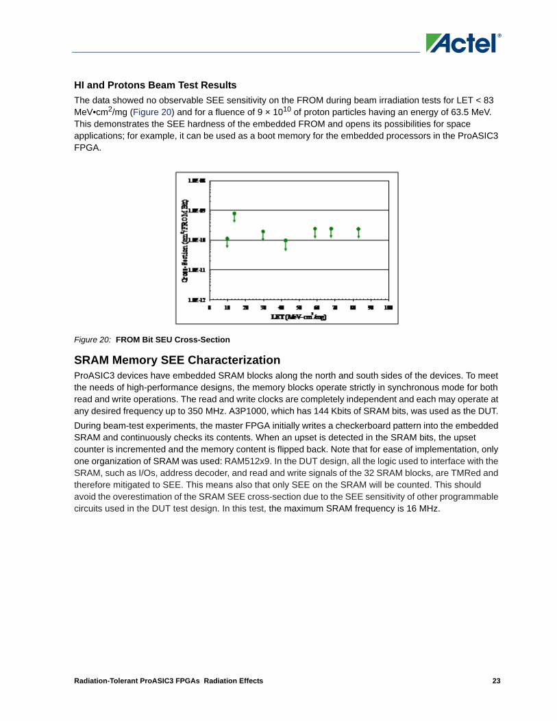
HI and Protons Beam Test ResultsThe data showed no observable SEE sensitivity on the FROM during beam irradiation tests for LET < 83 MeV•cm2/mg (Figure 20) and for a fluence of 9 × 10¹⁰ of proton particles having an energy of 63.5 MeV. This demonstrates the SEE hardness of the embedded FROM and opens its possibilities for space applications; for example, it can be used as a boot memory for the embedded processors in the ProASIC3 FPGA.
SRAM Memory SEE CharacterizationProASIC3 devices have embedded SRAM blocks along the north and south sides of the devices. To meet the needs of high-performance designs, the memory blocks operate strictly in synchronous mode for both read and write operations. The read and write clocks are completely independent and each may operate at any desired frequency up to 350 MHz. A3P1000, which has 144 Kbits of SRAM bits, was used as the DUT. During beam-test experiments, the master FPGA initially writes a checkerboard pattern into the embedded SRAM and continuously checks its contents. When an upset is detected in the SRAM bits, the upset counter is incremented and the memory content is flipped back. Note that for ease of implementation, only one organization of SRAM was used: RAM512x9. In the DUT design, all the logic used to interface with the SRAM, such as I/Os, address decoder, and read and write signals of the 32 SRAM blocks, are TMRed and therefore mitigated to SEE. This means also that only SEE on the SRAM will be counted. This should avoid the overestimation of the SRAM SEE cross-section due to the SEE sensitivity of other programmable circuits used in the DUT test design. In this test, the maximum SRAM frequency is 16 MHz.
Figure 20: FROM Bit SEU Cross-Section
Radiation-Tolerant ProASIC3 FPGAs Radiation Effects 23

The block diagram of the test design is given in Figure 21.
The test results show no SRAM SEE cross-section dependence on the frequency, indicating that most of the SET effects on the peripheral combinational logic are filtered out and only SEU on the SRAM blocks are counted. Also, no MBU were observed in the SRAM bits. Measured SEU cross-sections are given in Figure 22. The saturation cross-section is approximately 4.22 × 10⁻⁸ cm2/SRAM-bit.
The LET threshold is around 0.5 MeV-cm2/mg, which is considered very low, but correlates well with the published SEU cross-sections of 0.13-µm CMOS SRAM bits from other vendors [Rezgui et al., 2004]. It should be mentioned also that additional testing should be done to find out about MBU in the SRAM
Figure 21: Block Diagram of the SRAM Test Design
Figure 22: HI SRAM Bit SEU Cross-Section
24 Radiation-Tolerant ProASIC3 FPGAs Radiation Effects

blocks. Static tests should be used where the SRAM is read at the end of each run, preferably irradiated at low fluxes to avoid hiding some of the bit errors because of multiple hits. SEE mitigation solutions for the SRAM, based mainly on an EDAC approach such as the one employed for the SRAM of RTAX-S FPGAs [Wang et al., 04b] have been developed and are available for use with RT ProASIC3 products.Finally, in comparison with the other FPGA resources, the embedded SRAM blocks, when operated at 16 MHz, showed an SEU cross-section in protons beams, for a cocktail of energies of 63.5, 30, 19.5, and 16.5 MeV. The results obtained are shown in Figure 23. Additional tests shall be performed to establish the threshold proton energy to induce upsets in the SRAM bits.
Figure 23: Proton SRAM Bit SEU Cross-Section
Radiation-Tolerant ProASIC3 FPGAs Radiation Effects 25

Preliminary Studies of TID Effects on SEE Sensitivities
Proton Characterization of the Programming and Erase CircuitryOne major advantage of the flash-based FPGAs compared to the previous generation of Actel FPGAs, based on antifuse technology, is the reprogrammability feature. However, during erase and reprogramming of the part, high voltages are applied (±17.5 V) and one might think that there is a risk of permanent damage on the FG cells or other overhead circuitry if an ion hit during that mode. Therefore, radiation test experiments during the erase and the programming of this part are required to measure the SEE sensitivity of this specific part of the FPGA (charge pumps) and the overall consequences from an ion hit.Ten A3P250-PQ208 circuits have been exercised in proton beams during the erase, reprogramming, and verification of the programmed FG cells. The shift register design using 98% of the FPGA logic tiles (A3P250-PQ208) was used as a reference design. For each beam run, consecutive erase, reprogramming, and verify cycles are launched and the functionality of the design is always checked at the end of each run. At least four full cycles of erase, program, and verify cycle are executed during each beam run; each cycle requires 41 seconds. Each run exposes a new DUT to a dose of 13.4 Krad due to proton beam exposition and uses a fluence of 1011 of proton particles. Table 3 summarizes the results.
Three types of behavior have been observed during the proton irradiation testing, as summarized in Table 3. Type 1 is showing the case where four erase, programming, and verifying cycles have been performed without any failure, including the design’s operation. Type 2 shows the one case where only one verifying failure has been observed (second cycle), which could be due to the programming of false information in the FG cells (ON state instead of OFF state and vice versa). This type of error is easily mitigated by running a second cycle of erase, reprogramming, and verifying of the FG cells, allowing the DUT to recover normal operation, and has a cross-section of 10-12 cm2/FPGA. Type 3 is the case where a fifth cycle was started and did fail because we reached a dose of 13.4 Krad, which is considered high for the normal operation of the charge pump circuit, according to TID tests in gamma rays at DMEA, shown above in the "TID Characterization" section on page 6 and also considering the high dose rate exercised in this case (58 rad/s).During all these runs, there was no permanent damage on the circuit and all errors that have been observed during these test cycles disappeared after annealing. Indeed, the two parts that failed programming on the fifth time recovered functionality after annealing of the DUT at room temperatures for many days. Although these preliminary results are encouraging and since the annealing effects on the floating gates are still under study, it is recommended that you avoid erasing and reprogramming the DUT in-beam or off-beam after its exposure to a dose higher than 16 Krad. This statement is valid only if the applied dose rate from heavy ions, protons, or gamma is around 50 rad/s, as required by the JEDEC test standards [MIL-STD-883G, TM1019.7]. In the case of the actual proton testing, the dose rate was around 58 rad/s, which might explain the observation of some failures on the fifth cycle of erase and programming at 13.4 Krad. Also, the cross-section of writing wrong information (10-12 cm2/FPGA) could be
Table 3: Programming and Erase Error Modes in Proton BeamsBehavior Type Error Description Number of DUTs1 All 4 programming and erase cycles have passed successfully 9
2 One erase/program cycle among 4 failed and the next one passed 1
3 Failure of the fifth cycle of erase / programming because of total exposure to TID (13.4 Krad) requiring annealing
2
26 Radiation-Tolerant ProASIC3 FPGAs Radiation Effects

fundamentally due to the very little SEE sensitivity to protons of the ProASIC3 FPGA. Heavy ion data is hence required to confirm that no catastrophic failures could result from programming and erasing in-beam, since the FPGA’s SEE sensitivities under HI irradiation are much higher relative to the proton sensitivity.
Testing Beyond the TID LimitMost of the collected data for the measurements of the SEE cross-sections in this chapter has been obtained for TID less than 25 Krad in gamma rays. Data provided in the "TID Characterization" section on page 6 showed the TID performance of this device to be 16 Krad for the programming and erase circuitry and 22 Krad for the FPGA core itself (the FG cells). For the latter, the TID performance was mainly obtained when a degradation of 10% in the propagation delay of the logic tiles configured as a chain of buffers is attained, but no permanent damage on the FPGA was noted.The purpose of this new specific test is to check design functionality and SEE performance for TID higher than 25 Krad as well as the maximum TID to which the design is still functional. The SRAM test design was selected for this study, since it uses various resources of the FPGA: 8.24% of the FPGA logic tiles (configured as combinational or sequential logic), 100% of the embedded SRAM memories, the embedded PLL and FROM, and 44% of the I/Os. This design was also selected because of the high SEE sensitivity of the SRAM compared to the other FPGA resources, which could help in monitoring the functionality and the SEE cross-sections if they do increase.The DUT was exposed to a beam for 5 consecutive runs, each at a fluence of 4x10¹⁰ of 16.5 MeV proton particles. This corresponds approximately to a TID of 15 Krad per run, and to a total of 75 Krad for the five runs. During all these runs, the DUT design was functional and the error cross-section per run was consistent without any noticeable increase in the SEE sensitivities, as shown in Table 4. It should also be noted that for all of the five runs, the detection of errors stops with the end of the beam time. This confirms that the FG cells are still functional upon a TID of 75 Krad. However, upon the start of the sixth run, the design stopped functioning, which could be due to a high charge loss in the FG cells. After four months of annealing in room temperature, the design did recover functionality but not the reprogramming capability. Time is needed to check whether more annealing time will allow recovery of the full operation of the charge pumps needed for the FPGA re-programming.
An accurate estimation of the TID effects on the SEE cross-sections requires a better measurement of the accumulated dose. Indeed, until today, only gamma rays could provide an accurate measurement of the exposed dose and therefore it would be advised to expose the part to a certain dose in gamma rays and then measure the SEE cross-sections, within 2 hours or a few days if transported in dry ice to avoid annealing effects.
Table 4: TID Effects from Proton Irradiation (Energy = 16.5 MEV) on the SEE Cross-Sections of an SRAM-Bit
RunAccumulated
TID [Krad]SRAM Bit SEE Cross-Section
[MeV-cm2/mg]Fluence
[16.5 MeV Proton-Particles]1 15 2.48 × 10⁻¹⁴ 4 × 10¹⁰
2 30 2.29 × 10⁻¹⁴ 4 × 10¹⁰
3 45 2.51 × 10⁻¹⁴ 4 ×10¹⁰
4 60 2.80 × 10⁻¹⁴ 4 × 10¹⁰
5 75 2.71 × 10⁻¹⁴ 4 × 10¹⁰
6 90 Design lost functionality right in the beginning of the run but recovered after annealing in room temperature.
4 × 10¹⁰
Radiation-Tolerant ProASIC3 FPGAs Radiation Effects 27

In addition, it should be mentioned also that among the 60 parts, tested in all the HI experiments, 59 of them have recovered the DUT programming and erasing capabilities after many months of annealing in room temperature and did never lose functionalities in- or off-beam. The TID for the 59 parts varied between 5 and 40 Krad. The only DUT that did not recover the programming capability was exposed to a TID of 41.5 Krad. Knowing that after annealing we could erase this part led us to assume that we might need more time to be able to reprogram it again. All of the 24 parts that have been tested in protons could be erased but seven of them could not be reprogrammed. Time is needed to make sure that the seven remaining parts will recover this feature.The main conclusion from these test experiments is that most of the tested parts did recover the programming and erase features after annealing in room temperature for many months. None of them lost functionality for doses that approximate 40 Krad even at the highest LET (83 MeV-cm2/mg) or 63.5 MeV in protons. It is clear, though, that the recovery of the erase functionality is much quicker than the recovery of the programming capability. This is certainly not a quantitative study but rather qualitative to make sure that there is no permanent damage from HI or protons on the part due to TID. Additional testing is hence mandatory to calculate accurately the annealing effects on the FG cells and the circuitry used for the erase and the reprogramming of the FPGA. More work has been done since to show and explain the annealing effects on the flash memories [Bagatin et al., 09].
ConclusionThis report detailed the extensive radiation tests of the new radiation-tolerant flash based-FPGAs (RT ProASIC3) to determine its sensitivities to TID and SEE as well as some suitable methodologies for mitigation of these effects. Based on the measurements of the degradation in the propagation delay of an inverter-string, the TID performance of the RT ProASIC3 part was characterized to be 22 Krad. However, if reprogramming in space is performed, the TID limit of this part can be improved to 40 Krad. Note that safe reprogramming of RT ProASIC3 FPGAs is advisable only up to 16 Krad because of the TID effects on the programming control circuits.Furthermore, the obtained results from the SEE characterization showed some radiation sensitivity in most of the programmable architectural features of the FPGA; the exception is the embedded FROM, which is very radiation hard. If mitigation solutions of TMR and SET filtering are adopted for the logic and clock in ProASIC3 FPGAs, the only remaining cross-section would be due to the transient event on the I/O banks used for SE or LVDS I/Os observable mostly at high frequencies. On the other hand, if a complete SEE immunity is required at high frequencies (50 MHz and above), triplication of I/Os is mandatory in addition to their separation on three different I/O banks. Finally, as expected for a nonvolatile FPGA, no observed error-event required a reconfiguration of the flash-based FPGA nor were there any destructive SEE events even during the erase, the programming, and the verifying of the FPGA. SEU mitigation by software user-selective-TMR and software Intellectual Property (IP) to implement EDAC for the embedded SRAMs are available to the user of radiation-tolerant flash-based FPGAs.
By Sana RezguiSenior Principal Engineer and Project Lead for Radiation Effects, Actel Corporation
Prior to joining Actel in 2006, Sana Rezgui has held research, consultant, and engineering positions with JPL/NASA, NEE ANN Polytechnic of Singapore and Xilinx. She holds bachelor's and master's degrees in electrical engineering from ENIT and UPS in Toulouse, France, respectively, as well as a doctorate in microelectronics from INPG in France.
28 Radiation-Tolerant ProASIC3 FPGAs Radiation Effects

AcknowledgementsI am greatly indebted to J. J. Wang, Brian Cronquist, John McCollum, Minal Sawant, and Ken O’Neill from Actel Corporation for many fruitful discussions and suggestions. I would like to express a great thanks to Natalie Charest, Eric Chan Tung, Yinming Sun, and Durwyn D’Silva from the University Of Toronto, Canada, who worked as intern-students in Actel Corporation, each for a year period.
ReferencesBagatin, M.; Gerardin, S.; Cellere, G.; Paccagnella, A.; Visconti, A.; Bonanomi, M.; Beltrami, S. (2009). "Error Instability in Floating Gate Flash Memories Exposed to TID," NSREC 2009, to be published at IEEE TNS, Vol. 56, NO. 6, Dec. 2009, Quebec City, Quebec, Canada.Baze, M. P.; Wert, J.; Clement, J. W.; Hubert, M.G.; Witulski, A.; Amusan, O.A.; Massengill, L. and McMorrow, D. (2006). "Propagating SET Characterization Technique for Digital CMOS Libraries," IEEE TNS, Vol. 53, No. 6, Dec. 2006, pp 3472-3478.Berg, M.; Wang, J.J.; Ladbury, R.; Buchner, S.; Kim, H.; Howard, J.; Label, K.; Phan, A.; Irwin, T. and Friendlich, M. (2006). "An Analysis of Single Event Upset Dependencies on High Frequency and Architectural Implementations within Actel RTAX-S Family Field Programmable Gate Arrays," IEEE TNS, Vol. 53, No. 6, Dec. 2006, pp 3569-3574.Brown, W.D. and Brewer, J. (2002). "Nonvolatile Semiconductor Memory Technology: A Comprehensive Guide to Understanding and Using NVSM Devices," IEEE Press Series on Microelectronic Systems.Carmichael, C. (2001) "Triple Module Redundancy Design Techniques for Virtex FPGAs," Xilinx Application Note XAPP197, Nov. 2001, available at www.xilinx.com/bvdocs/appnotes/xapp197.pdf.Balasubramanian, A.; Bhuva, B.L.; Black, J.D.; Massengill, L.W. (2005). "RHBD Techniques for Mitigating Effects of Single-Event Hits Using Guard-Gates," IEEE TNS, Vol. 52, No. 6, Dec. 2005, pp 2531 – 2535.Cellere, G.; Paccagnella, A.; Visconti, A.; Bonanomi, M.; Caprara, P. and Lora, S. (2004). "A Model for TID Effects on Floating gate Memory Cells," IEEE TNS, Vol. 51, No. 6, Dec. 2004, pp 3753-3758.Guertin, S.; Nguyen, D. & Patterson, J. (2006). "Microdose Induced Dose Data Loss on floating Gate Memories," IEEE TNS, Vol. 53, No. 6, Dec. 2006, pp 3518-3524.MIL-STD-883G, TM1019.7, http://www.aspentechnologies.com/files/rur89tn69a.pdf.Mitra, S.; Zhang, M.; Seifert, N.; Gill, B.; Waqas, S.; Kim, K.S. (2006). "Combinational Logic Soft Error Correction," IEEE ITC, Nov. 2006.Mavis, D. and Eaton, P. (2007). "SEU and SEU Modeling and Mitigation in Deep-Submicron Technologies," IRPS 2007, pp 293-305, Albuquerque, USA.Morris, K. (2006). FPGA Journal, available at http://www.fpgajournal.com/articles_2006/pdf/20060829_igloo.pdf.Palkuti, L.J.; and LePage, J.J. (1982). "X-rays Wafer Probe for Total Dose Testing”, IEEE TNS, Vol. 29, No. 6, Dec. 1982, pp 1832-1837.ProASIC3 Flash Family FPGAs datasheet, available at http://www.actel.com/documents/PA3_DS.pdf.Quinn, H.; Graham, P.; Krone, J.; Caffrey, M. and Rezgui, S. (2005). "Radiation-Induced Multi-Bit Upsets in SRAM-Based FPGAs," IEEE TNS, Vol. 53, No. 6, Dec. 2005, pp. 2455-2461.
Radiation-Tolerant ProASIC3 FPGAs Radiation Effects 29

Rezgui, S.; Swift, G. and Xilinx SEE Consortium (2004). "Xilinx Single Event Effects First Consortium Report Virtex-II Static SEU Characterization," available at http://parts.jpl.nasa.gov/docs/swift/virtex2_0104.pdf.Rezgui, S.; Wang, J.J.; Chan Tung, E.; McCollum, J. and Cronquist, B. (2007). "New Methodologies for SET Characterization and Mitigation in Flash-Based FPGAs," IEEE TNS, Vol. 54, No. 6, Dec. 2007, pp 2512-2524.Rezgui, S.; Wang, J.J.; Sun, Y.; Cronquist, B. and McCollum, J. (2008a). "New Reprogrammable and Non-Volatile Radiation Tolerant FPGA: RTA3P," IEEE Aerospace 2008, Big Sky, MT.Rezgui, S.; Wang, J.J.; Sun, Y.; Cronquist, B. and McCollum, J. (2008b). "Configuration and Routing Effects on the SET Propagation in Flash-Based FPGAs," IEEE TNS, Vol. 55, No. 6, Dec. 2008, pp 3328-3335.Rezgui, S.; Wang, J.J.; Won, R. and McCollum, J. (2009). "Design and Layout Effects on SET Propagation in ASIC and FPGA 90-nm Test Structures," NSREC 2009, to be published at IEEE TNS, Vol. 56, No. 6, Dec. 2009, Quebec City, Quebec, Canada.Snyder, E.S.; McWhorter, P.J.; Dellin, T.A. and Sweetman, J.D. (1989). "Radiation Response of Floating Gate EEPROM Memory Cells," IEEE TNS, Vol. 36, No. 6, Dec. 1989, pp 2131-2139.Shuler, R.L.; Kouba, C. and O’Neill, P.M. (2005). "SEU Performance of TAG Based Flip-Flops," IEEE TNS, Vol. 52, No. 6, Dec. 2005, pp 2550-2553.Shuler, R.L.; Balasubramanian, A.; Narasimham, B.; Bhuva, B.L.; O’Neil, P.M. and C. Kouba (2006). "The Effectiveness of TAG or Guard-Gates in SET Suppression Using Delay and Dual-Rail Configurations at 0.35 µm," IEEE TNS, Vol. 53, No. 6, Dec. 2006, pp 3428-3431.Swift, G.; Rezgui, S.; George, J.; Carmichael, C.; Napier, M.; Maksimowictz, J.; Moore, J.; Lesea, A.; Koga, R. and Wrobel, T.F. (2004). "Dynamic Testing of Xilinx Virtex-II Field Programmable Gate Array (FPGA) Input/Output Blocks (IOBs)," IEEE TNS, Vol. 51, No. 6, Dec. 2004, pp 3469-3479.Wang, J.J.; Samiee, S.; Chen, H.S.; Huang, C.K.; Cheung, M.; Borillo, J.; Sun, S.N.; Cronquist, B. and McCollum, J. (2004a). "Total Ionizing Dose Effects on Flash-Based Field Programmable Gate Array," IEEE TNS, Vol. 51, No. 6, Dec. 2004, pp 3759-3766.Wang, J.J. (2004b). "RTAX EDAC-RAM Single Event Upset Test Report," available at http://www.actel.com/documents/RTAX-S%20SEE%20EDAC%20RAM.pdf Wang, J.J.; Kuganesan, G.; Charest, N. and Cronquist, B. (2006a). "Biased-Irradiation Characteristics of the Floating Gate Switch in FPGA," NSREC 2006, Ponte Vedra, FL.Wang, J.J.; Charest, N.; Kuganesan, G.; Huang, C.K.; Yip, M.; Chen, H.S.; Borillo, J.; Samiee, S.; Dhaoui F.; Sun, J.; Rezgui, S.; McCollum, J. and Cronquist, B. (2006b). "Investigating and Modeling Total Ionizing Dose and Heavy Ion effects in Flash-Based Field Programmable Gate Array," RADECS 2006, Athens, Greece.
30 Radiation-Tolerant ProASIC3 FPGAs Radiation Effects

Actel Hong KongRoom 2107, China Resources Building26 Harbour RoadWanchai, Hong KongPhone +852 2185 6460Fax +852 2185 6488www.actel.com.cn
© 2010 Actel Corporation. All rights reserved. Actel, Actel Fusion, IGLOO, Libero, Pigeon Point, ProASIC, SmartFusion and the associated logos are trademarks or registeredtrademarks of Actel Corporation. All other trademarks and service marks are the property of their respective owners.
51000010-0/4.10
Actel Corporation2061 Stierlin CourtMountain View, CA94043-4655USAPhone 650.318.4200Fax 650.318.4600
Actel Europe Ltd.River Court, Meadows Business ParkStation Approach, BlackwateryCamberley Surrey GU17 9ABUnited KingdomPhone +44 (0) 1276 609 300Fax +44 (0) 1276 607 540
Actel JapanEXOS Ebisu Building 4F1-24-14 Ebisu Shibuya-kuTokyo 150 JapanPhone +81.03.3445.7671Fax +81.03.3445.7668http://jp.actel.com
Actel is the leader in low power FPGAs and mixed signal FPGAs and offers the most comprehensive portfolio of systemand power management solutions. Power Matters. Learn more at www.actel.com.