rail-to-rail 1.1 v dual and quad nanopower comparators · rail-to-rail 1.1 v dual and quad...
TRANSCRIPT

This is information on a product in full production.
July 2017 DocID024119 Rev 4 1/25
TS882 TS884
Rail-to-rail 1.1 V dual and quad nanopower comparators
Datasheet - production data
Features• Ultra-low current consumption: 220 nA typ./op.
• Propagation delay: 2 µs typ.
• Rail-to-rail inputs
• Push-pull outputs
• Supply operation from 1.1 V to 5.5 V
• Wide temperature range: -40 to +125 °C
• ESD tolerance: 8 kV HBM / 300 V MM
• Dual version available in MiniSO8 and DFN8(2 x 2 mm) package
• Quad version available in SO14, TSSOP14and QFN16 3 x 3 mm package
Related product
• See the TS881 datasheet for single operatorwith smaller package.
Applications• Portable systems
• Signal conditioning
• Medical
• Automotive
DescriptionThe TS882 is a dual and the TS884 device a quad comparator featuring ultra-low supply current (220 nA typical per operator with output high, VCC = 1.2 V, no load) with rail-to-rail input and output capability. The performance of these comparators allows them to be used in a wide range of portable applications. The TS882 and TS884 devices minimize battery supply leakage and therefore enhance battery lifetime.
Operating from 1.1 to 5.5 V supply voltage, these comparators can be used over a wide temperature range (-40 to +125 °C) keeping the current consumption at an ultra-low level.
QFN16 (3 x 3 mm)
SO14TSSOP14
DFN8 (2 x 2 mm) MiniSO8
Table 1. Device summary
Order code Temperature range Package Packaging Marking
TS882IST
-40 to +125 °C
MiniSO8
Tape and reel
K514
TS882IYST(1) MiniSO8 (Automotive grade)
K524
TS882IQ2T DFN8 2 x 2 mm K56
TS884IDT
-40 to +125 °C
SO14
Tape and reel
S884I
TS884IPT TSSOP14 S884I
TS884IQ4T QFN16 3 x 3 mm K514
1. Qualified and characterized according to AEC Q100 and Q003 or equivalent, advanced screening according to AEC Q001& Q002 or equivalent
www.st.com
Contents TS882, TS884
2/25 DocID024119 Rev 4
Contents
1 Pin description . . . . . . . . . . . . . . . . . . . . . . . . . . . . . . . . . . . . . . . . . . . . . 3
2 Absolute maximum ratings and operating conditions . . . . . . . . . . . . . 4
3 Electrical characteristics . . . . . . . . . . . . . . . . . . . . 5
4 Package information . . . . . . . . . . . . . . . . . . . . . . . . . . . . . . . . . . . . . . . . 15
4.1 DFN8 2 x 2 mm package information . . . . . . . . . . . . . . . . . . . . . . . . . . . 16
4.2 MiniSO8 package information . . . . . . . . . . . . . . . . . . . . . . . . . . . . . . . . . 18
4.3 SO14 package information . . . . . . . . . . . . . . . . . . . . . . . . . . . . . . . . . . . . 19
4.4 QFN16 3 x 3 package information . . . . . . . . . . . . . . . . . . . . . . . . . . . . . . 20
4.5 TSSOP14 package information . . . . . . . . . . . . . . . . . . . . . . . . . . . . . . . . 23
5 Revision history . . . . . . . . . . . . . . . . . . . . . . . . . . . . . . . . . . . . . . . . . . . 24
DocID024119 Rev 4 3/25
TS882, TS884 Pin description
25
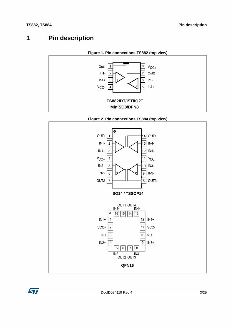
1 Pin description
Figure 1. Pin connections TS882 (top view)
Figure 2. Pin connections TS884 (top view)
TS882IDT/IST/IQ2T
MiniSO8/DFN8
SO14 / TSSOP14
QFN16
Absolute maximum ratings and operating conditions TS882, TS884
4/25 DocID024119 Rev 4
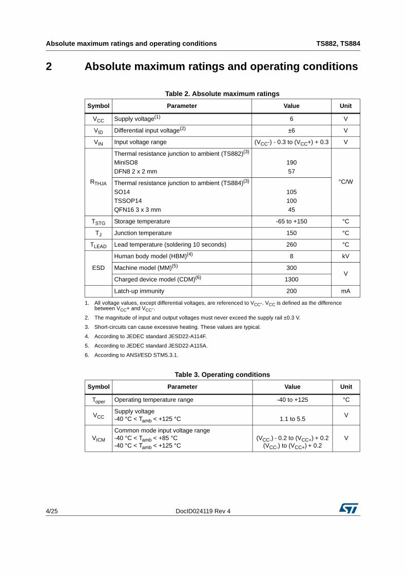
2 Absolute maximum ratings and operating conditions
Table 2. Absolute maximum ratings
Symbol Parameter Value Unit
VCC Supply voltage(1)
1. All voltage values, except differential voltages, are referenced to VCC-. VCC is defined as the difference between VCC+ and VCC-.
6 V
VID Differential input voltage(2)
2. The magnitude of input and output voltages must never exceed the supply rail ±0.3 V.
±6 V
VIN Input voltage range (VCC-) - 0.3 to (VCC+) + 0.3 V
RTHJA
Thermal resistance junction to ambient (TS882)(3)
MiniSO8
DFN8 2 x 2 mm
3. Short-circuits can cause excessive heating. These values are typical.
190
57
°C/WThermal resistance junction to ambient (TS884)(3)
SO14TSSOP14QFN16 3 x 3 mm
10510045
TSTG Storage temperature -65 to +150 °C
TJ Junction temperature 150 °C
TLEAD Lead temperature (soldering 10 seconds) 260 °C
ESD
Human body model (HBM)(4)
4. According to JEDEC standard JESD22-A114F.
8 kV
Machine model (MM)(5)
5. According to JEDEC standard JESD22-A115A.
300V
Charged device model (CDM)(6)
6. According to ANSI/ESD STM5.3.1.
1300
Latch-up immunity 200 mA
Table 3. Operating conditions
Symbol Parameter Value Unit
Toper Operating temperature range -40 to +125 °C
VCCSupply voltage-40 °C < Tamb < +125 °C 1.1 to 5.5
V
VICM
Common mode input voltage range-40 °C < Tamb < +85 °C-40 °C < Tamb < +125 °C
(VCC-) - 0.2 to (VCC+) + 0.2(VCC-) to (VCC+) + 0.2
V

DocID024119 Rev 4 5/25
TS882, TS884 Electrical characteristics
25
3 Electrical characteristics
Table 4. VCC = +1.2 V, Tamb = +25 °C, VICM = VCC/2 (unless otherwise specified)(1)
Symbol Parameter Test conditions Min. Typ. Max. Unit
VIO Input offset voltage(2) Tamb = +25 °C
-40 °C < Tamb < +125 °C -6
1
6mV
ΔVIO Input offset voltage drift -40 °C < Tamb < +125 °C 3 µV/°C
VHYST Input hysteresis voltage(3) Tamb = +25 °C-40 °C < Tamb < +125 °C 1.5
2.44.2
mV
IIO Input offset current(4) Tamb = +25 °C-40 °C < Tamb < +125 °C
10100
pA
IIB Input bias current(4) Tamb = +25 °C-40 °C < Tamb < +125 °C
1 10100
pA
ICC Supply current per operator
No load, output low, VID = -0.1 V-40 °C < Tamb < +125 °C
No load, output high, VID = +0.1 V-40 °C < Tamb < +125 °C
300
220
450
350
nA
ISC Short-circuit currentSourceSink
1.01.7
mA
VOH Output voltage highIsource = 0.2 mA-40 °C < Tamb < +85 °C-40 °C < Tamb < +125 °C
1.131.101.00
1.15V
VOL Output voltage lowIsink = 0.2 mA-40 °C < Tamb < +85 °C-40 °C < Tamb < +125 °C
35 506070
mV
CMRR Common mode rejection ratio0 < VICM < VCC-40 °C < Tamb < +125 °C 50
68dB
TPLHPropagation delay(low to high)
f = 1 kHz, CL = 30 pF, RL = 1 MΩOverdrive = 10 mV-40 °C < Tamb < +125 °C
Overdrive = 100 mV-40 °C < Tamb < +125 °C
5.5
2.1
1113
3.13.4
µs
TPHLPropagation delay(high to low)
f = 1 kHz, CL = 30 pF, RL = 1 MΩOverdrive = 10 mV-40 °C < Tamb < +125 °C
Overdrive = 100 mV-40 °C < Tamb < +125 °C
5.1
1.9
810
2.63.1
µs
TR Rise time (10% to 90%)CL = 30 pF, RL = 1 MΩ
100 ns

Electrical characteristics TS882, TS884
6/25 DocID024119 Rev 4
TF Fall time (90% to 10%)CL = 30 pF, RL = 1 MΩ
110 ns
TON Power-up time 1.1 1.7 ms
1. All values over the temperature range are guaranteed through correlation and simulation. No production test is performed at the temperature range limits.
2. The offset is defined as the average value of positive and negative trip points (input voltage differences requested to change the output state in each direction).
3. The hysteresis is a built-in feature of the TS882 device. It is defined as the voltage difference between the trip points.
4. Maximum values include unavoidable inaccuracies of the industrial tests.
Table 4. VCC = +1.2 V, Tamb = +25 °C, VICM = VCC/2 (unless otherwise specified)(1) (continued)
Symbol Parameter Test conditions Min. Typ. Max. Unit
Table 5. VCC = +2.7 V, Tamb = +25 °C, VICM = VCC/2 (unless otherwise specified)(1)
Symbol Parameter Test conditions Min. Typ. Max. Unit
VIO Input offset voltage(2) Tamb = +25 °C-40 °C < Tamb < +125 °C -6
16
mV
ΔVIO Input offset voltage drift -40 °C < Tamb < +125 °C 3 µV/°C
VHYST Input hysteresis voltage(3) Tamb = +25 °C
-40 °C < Tamb < +125 °C 1.6
2.7
4.2mV
IIO Input offset current(4) Tamb = +25 °C
-40 °C < Tamb < +125 °C10
100pA
IIB Input bias current(4) Tamb = +25 °C
-40 °C < Tamb < +125 °C1 10
100pA
ICC Supply current per operator
No load, output low, VID = -0.1 V-40 °C < Tamb < +125 °C
No load, output high, VID = +0.1 V-40 °C < Tamb < +125 °C
310
220
450
350
nA
ISC Short-circuit currentSourceSink
1013
mA
VOH Output voltage highIsource = 2 mA-40 °C < Tamb < +85 °C-40 °C < Tamb < +125 °C
2.482.402.10
2.51V
VOL Output voltage lowIsink = 2 mA-40 °C < Tamb < +85 °C-40 °C < Tamb < +125 °C
130 210230310
mV
CMRR Common mode rejection ratio0 < VICM < VCC-40 °C < Tamb < +125 °C 55
74dB
TPLHPropagation delay(low to high)
f = 1 kHz, CL = 30 pF, RL = 1 MΩOverdrive = 10 mV-40 °C < Tamb < +125 °C
Overdrive = 100 mV-40 °C < Tamb < +125 °C
6.4
2.3
1214
3.03.7
µs
DocID024119 Rev 4 7/25
TS882, TS884 Electrical characteristics
25
TPHLPropagation delay(high to low)
f = 1 kHz, CL = 30 pF, RL = 1 MΩOverdrive = 10 mV-40 °C < Tamb < +125 °C
Overdrive = 100 mV-40 °C < Tamb < +125 °C
6.4
2.2
1214
3.03.7
µs
TR Rise time (10% to 90%) CL = 30 pF, RL = 1 MΩ 120 ns
TF Fall time (90% to 10%) CL = 30 pF, RL = 1 MΩ 130 ns
TON Power-up time 1.1 1.7 ms
1. All values over the temperature range are guaranteed through correlation and simulation. No production test is performed at the temperature range limits.
2. The offset is defined as the average value of positive and negative trip points (input voltage differences requested to change the output state in each direction).
3. The hysteresis is a built-in feature of the TS882. It is defined as the voltage difference between the trip points.
4. Maximum values include unavoidable inaccuracies of the industrial tests.
Table 5. VCC = +2.7 V, Tamb = +25 °C, VICM = VCC/2 (unless otherwise specified)(1) (continued)
Symbol Parameter Test conditions Min. Typ. Max. Unit
Table 6. VCC = +5 V, Tamb = +25 °C, VICM = VCC/2 (unless otherwise specified)(1)
Symbol Parameter Test conditions Min. Typ. Max. Unit
VIO Input offset voltage(2) Tamb = +25 °C
-40 °C < Tamb < +125 °C -6
1
6mV
ΔVIO Input offset voltage drift -40 °C < Tamb < +125 °C 3 µV/°C
VHYST Input hysteresis voltage(3) Tamb = +25 °C-40 °C < Tamb < +125 °C 1.6
3.14.2
mV
IIO Input offset current(4) Tamb = +25 °C-40 °C < Tamb < +125 °C
10100
pA
IIB Input bias current(4) Tamb = +25 °C-40 °C < Tamb < +125 °C
1 10100
pA
ICC Supply current per operator
No load, output low, VID = -0.1 V-40 °C < Tamb < +125 °C
No load, output high, VID = +0.1 V-40 °C < Tamb < +125 °C
350
250
500
400
nA
ISC Short-circuit currentSourceSink
3232
mA
VOH Output voltage highIsource = 2 mA-40 °C < Tamb < +85 °C-40 °C < Tamb < +125 °C
4.864.754.60
4.88V
VOL Output voltage lowIsink = 2 mA-40 °C < Tamb < +85 °C-40 °C < Tamb < +125 °C
90 130170280
mV
CMRR Common mode rejection ratio0 < VICM < VCC-40 °C < Tamb < +125 °C 55
78dB

Electrical characteristics TS882, TS884
8/25 DocID024119 Rev 4
SVR Supply voltage rejectionΔVCC = 1.2 V to 5 V-40 °C < Tamb < +125 °C 65
80dB
TPLHPropagation delay(low to high)
f = 1 kHz, CL = 30 pF, RL = 1 MΩOverdrive = 10 mV-40 °C < Tamb < +125 °C
Overdrive = 100 mV-40 °C < Tamb < +125 °C
8.3
2.5
1322
3.44.1
µs
TPHLPropagation delay(high to low)
f = 1 kHz, CL = 30 pF, RL = 1 MΩOverdrive = 10 mV-40 °C < Tamb < +125 °C
Overdrive = 100 mV-40 °C < Tamb < +125 °C
9.0
2.6
1619
3.54.2
µs
TR Rise time (10% to 90%) CL = 30 pF, RL = 1 MΩ 160 ns
TF Fall time (90% to 10%) CL = 30 pF, RL = 1 MΩ 150 ns
TON Power-up time 1.1 1.7 ms
1. All values over the temperature range are guaranteed through correlation and simulation. No production test is performed at the temperature range limits.
2. The offset is defined as the average value of positive and negative trip points (input voltage differences requested to change the output state in each direction).
3. The hysteresis is a built-in feature of the TS882 device. It is defined as the voltage difference between the trip points.
4. Maximum values include unavoidable inaccuracies of the industrial tests.
Table 6. VCC = +5 V, Tamb = +25 °C, VICM = VCC/2 (unless otherwise specified)(1) (continued)
Symbol Parameter Test conditions Min. Typ. Max. Unit

DocID024119 Rev 4 9/25
TS882, TS884 Electrical characteristics
25
Figure 3. Current consumption per operator vs. supply voltage - output low
Figure 4. Current consumption per operator vs. supply voltage - output high
Figure 5. Current consumption per operator vs. input common mode voltage at VCC = 1.2 V
Figure 6. Current consumption per operator vs. input common mode voltage at VCC = 5 V
Figure 7. Current consumption per operator vs. temperature
Figure 8. Current consumption per operator vs. toggle frequency

Electrical characteristics TS882, TS884
10/25 DocID024119 Rev 4
Figure 9. Input offset voltage vs. input common mode voltage at VCC = 1.2 V
Figure 10. Input hysteresis voltage vs. input common mode voltage at VCC = 1.2 V
Figure 11. Input offset voltage vs. input common mode voltage at VCC = 5 V
Figure 12. Input hysteresis voltage vs. input common mode voltage at VCC = 5 V
Figure 13. Input offset voltage vs. temperature Figure 14. Input hysteresis voltage vs. temperature

DocID024119 Rev 4 11/25
TS882, TS884 Electrical characteristics
25
Figure 15. Output voltage drop vs. sink current at VCC = 1.2 V
Figure 16. Output voltage drop vs. source current at VCC = 1.2 V
Figure 17. Output voltage drop vs. sink current at VCC = 2.7 V
Figure 18. Output voltage drop vs. source current at VCC = 2.7 V
Figure 19. Output voltage drop vs. sink current at VCC = 5 V
Figure 20. Output voltage drop vs. source current at VCC = 5 V
Electrical characteristics TS882, TS884
12/25 DocID024119 Rev 4
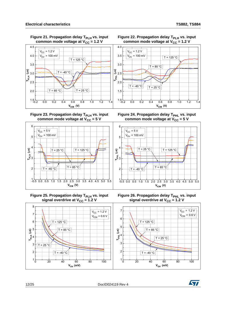
Figure 21. Propagation delay TPLH vs. input common mode voltage at VCC = 1.2 V
Figure 22. Propagation delay TPLH vs. input common mode voltage at VCC = 1.2 V
Figure 23. Propagation delay TPLH vs. input common mode voltage at VCC = 5 V
Figure 24. Propagation delay TPHL vs. input common mode voltage at VCC = 5 V
Figure 25. Propagation delay TPLH vs. input signal overdrive at VCC = 1.2 V
Figure 26. Propagation delay TPHL vs. input signal overdrive at VCC = 1.2 V

DocID024119 Rev 4 13/25
TS882, TS884 Electrical characteristics
25
Figure 27. Propagation delay TPLH vs. input signal overdrive at VCC = 5 V
Figure 28. Propagation delay TPHL vs. input signal overdrive at VCC = 5 V
Figure 29. Propagation delay TPLH vs. supply voltage for signal overdrive 10 mV
Figure 30. Propagation delay TPHL vs. supply voltage for signal overdrive 10 mV
Figure 31. Propagation delay TPLH vs. supply voltage for signal overdrive 100 mV
Figure 32. Propagation delay TPHL vs. supply voltage for signal overdrive 100 mV

Electrical characteristics TS882, TS884
14/25 DocID024119 Rev 4
Figure 33. Propagation delay vs. temperature for signal overdrive 10 mV
Figure 34. Propagation delay vs. temperature for signal overdrive 100 mV

DocID024119 Rev 4 15/25
TS882, TS884 Package information
25
4 Package information
In order to meet environmental requirements, ST offers these devices in different grades of ECOPACK® packages, depending on their level of environmental compliance. ECOPACK specifications, grade definitions and product status are available at: www.st.com. ECOPACK is an ST trademark.

Package information TS882, TS884
16/25 DocID024119 Rev 4
4.1 DFN8 2 x 2 mm package information
Figure 35. DFN8 2 x 2 mm package outline
Table 7. DFN8 2 x 2 mm package mechanical data (pitch 0.5 mm)
Symbol
Dimensions
Millimeters Inches
Min. Typ. Max. Min. Typ. Max.
A 0.51 0.55 0.60 0.020 0.022 0.024
A1 0.05 0.002
A3 0.15 0.006
b 0.18 0.25 0.30 0.007 0.010 0.012
D 1.85 2.00 2.15 0.073 0.079 0.085
D2 1.45 1.60 1.70 0.057 0.063 0.067
E 1.85 2.00 2.15 0.073 0.079 0.085
E2 0.75 0.90 1.00 0.030 0.035 0.039
e 0.50 0.020
L 0.50 0.020
ddd 0.08 0.003

DocID024119 Rev 4 17/25
TS882, TS884 Package information
25
Figure 36. DFN8 2 x 2 mm footprint recommendation
Package information TS882, TS884
18/25 DocID024119 Rev 4
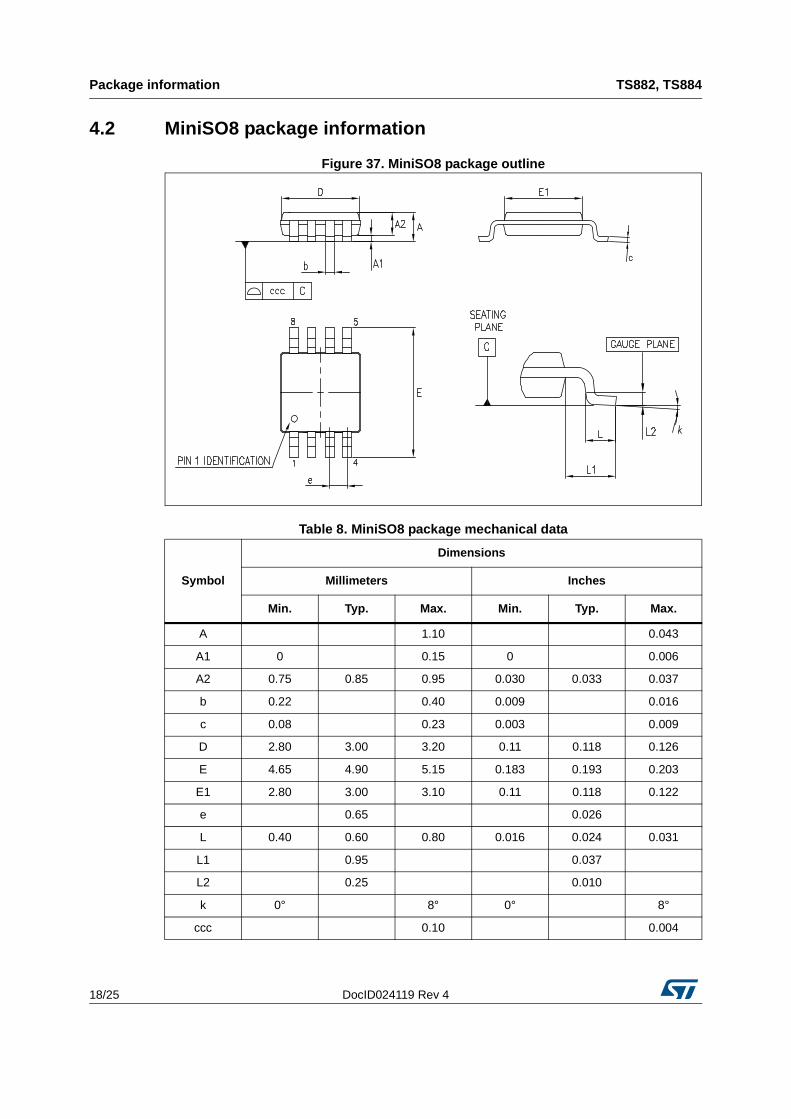
4.2 MiniSO8 package information
Figure 37. MiniSO8 package outline
Table 8. MiniSO8 package mechanical data
Symbol
Dimensions
Millimeters Inches
Min. Typ. Max. Min. Typ. Max.
A 1.10 0.043
A1 0 0.15 0 0.006
A2 0.75 0.85 0.95 0.030 0.033 0.037
b 0.22 0.40 0.009 0.016
c 0.08 0.23 0.003 0.009
D 2.80 3.00 3.20 0.11 0.118 0.126
E 4.65 4.90 5.15 0.183 0.193 0.203
E1 2.80 3.00 3.10 0.11 0.118 0.122
e 0.65 0.026
L 0.40 0.60 0.80 0.016 0.024 0.031
L1 0.95 0.037
L2 0.25 0.010
k 0° 8° 0° 8°
ccc 0.10 0.004

DocID024119 Rev 4 19/25
TS882, TS884 Package information
25
4.3 SO14 package information
Figure 38. SO14 package outline
Table 9. SO14 package mechanical data
Dimensions(1)
1. Drawing dimensions include “Single” and “Matrix” versions.
SymbolMillimeters Inches
NoteMin. Typ. Max. Min. Typ. Max.
A 1.35 1.75 0.05 0.068
A1 0.10 0.25 0.004 0.009
A2 1.10 1.65 0.04 0.06
B 0.33 0.51 0.01 0.02
C 0.19 0.25 0.007 0.009
D 8.55 8.75 0.33 0.34 (2)
2. Dimension “D” does not include mold flash, protrusions or gate burrs. Mold flash, protrusions or gate burrs shall not exceed 0.15 mm per side.
E 3.80 4.0 0.15 0.15
e 1.27 0.05
H 5.80 6.20 0.22 0.24
L 0.40 1.27 0.015 0.05
k 0° 8° 0° 8°
ddd 0.10 0.004
Package information TS882, TS884
20/25 DocID024119 Rev 4
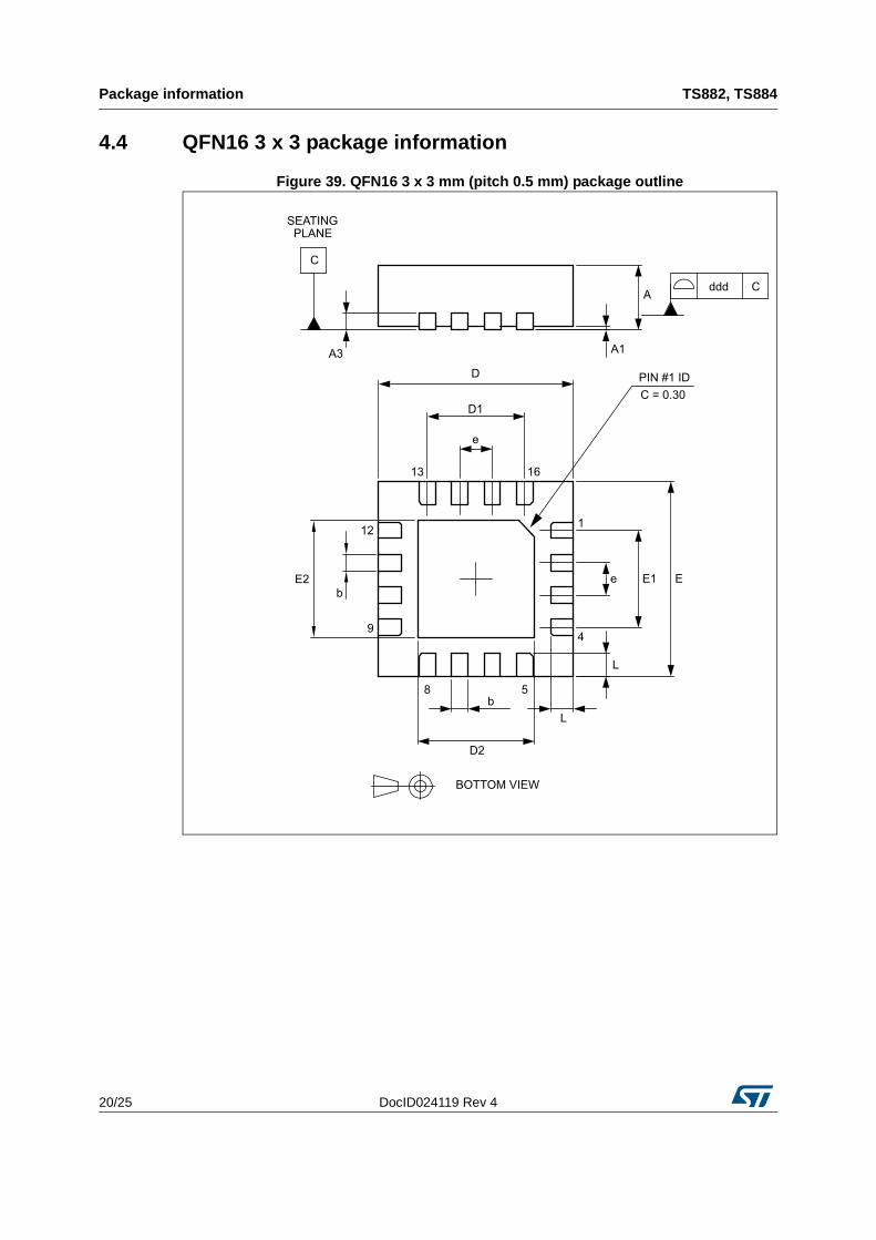
4.4 QFN16 3 x 3 package information
Figure 39. QFN16 3 x 3 mm (pitch 0.5 mm) package outline

DocID024119 Rev 4 21/25
TS882, TS884 Package information
25
Table 10. QFN16 3 x 3 mm (pitch 0.5 mm) package mechanical data
Symbol
Dimensions
Millimeters Inches
Min. Typ. Max. Min. Typ. Max.
A 0.80 0.90 1.00 0.031 0.035 0.039
A1 0.02 0.05 0.001 0.002
A3 0.20 0.008
b 0.18 0.25 0.30 0.007 0.010 0.012
D 2.85 3.00 3.15 0.112 0.118 0.124
D1 1.50 0.059
D2 See exposed pad variation See exposed pad variation
E 2.85 3.00 3.15 0.112 0.118 0.124
E1 1.50 0.059
E2 See exposed pad variation See exposed pad variation
e 0.45 0.50 0.55 0.018 0.020 0.022
L 0.30 0.40 0.50 0.012 0.016 0.020
ddd 0.08 0.003
Package information TS882, TS884
22/25 DocID024119 Rev 4
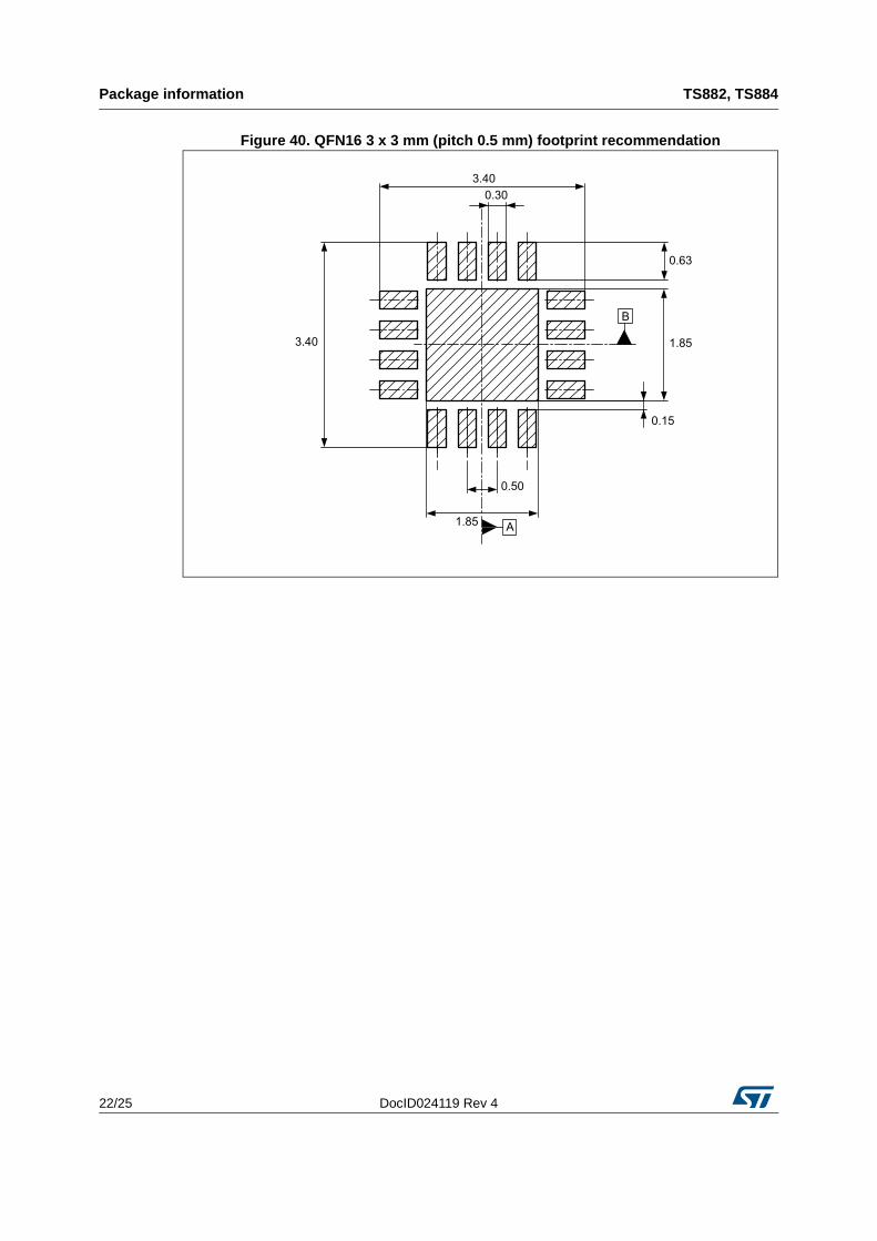
Figure 40. QFN16 3 x 3 mm (pitch 0.5 mm) footprint recommendation

DocID024119 Rev 4 23/25
TS882, TS884 Package information
25
4.5 TSSOP14 package information
Figure 41. TSSOP14 package outline
Table 11. TSSOP14 package mechanical data
Symbol
Dimensions
Millimeters Inches
Min. Typ. Max. Min. Typ. Max.
A 1.20 0.047
A1 0.05 0.15 0.002 0.004 0.006
A2 0.80 1.00 1.05 0.031 0.039 0.041
b 0.19 0.30 0.007 0.012
c 0.09 0.20 0.004 0.0089
D 4.90 5.00 5.10 0.193 0.197 0.201
E 6.20 6.40 6.60 0.244 0.252 0.260
E1 4.30 4.40 4.50 0.169 0.173 0.176
e 0.65 0.0256
L 0.45 0.60 0.75 0.018 0.024 0.030
L1 1.00 0.039
k 0° 8° 0° 8°
aaa 0.10 0.004
Revision history TS882, TS884
24/25 DocID024119 Rev 4
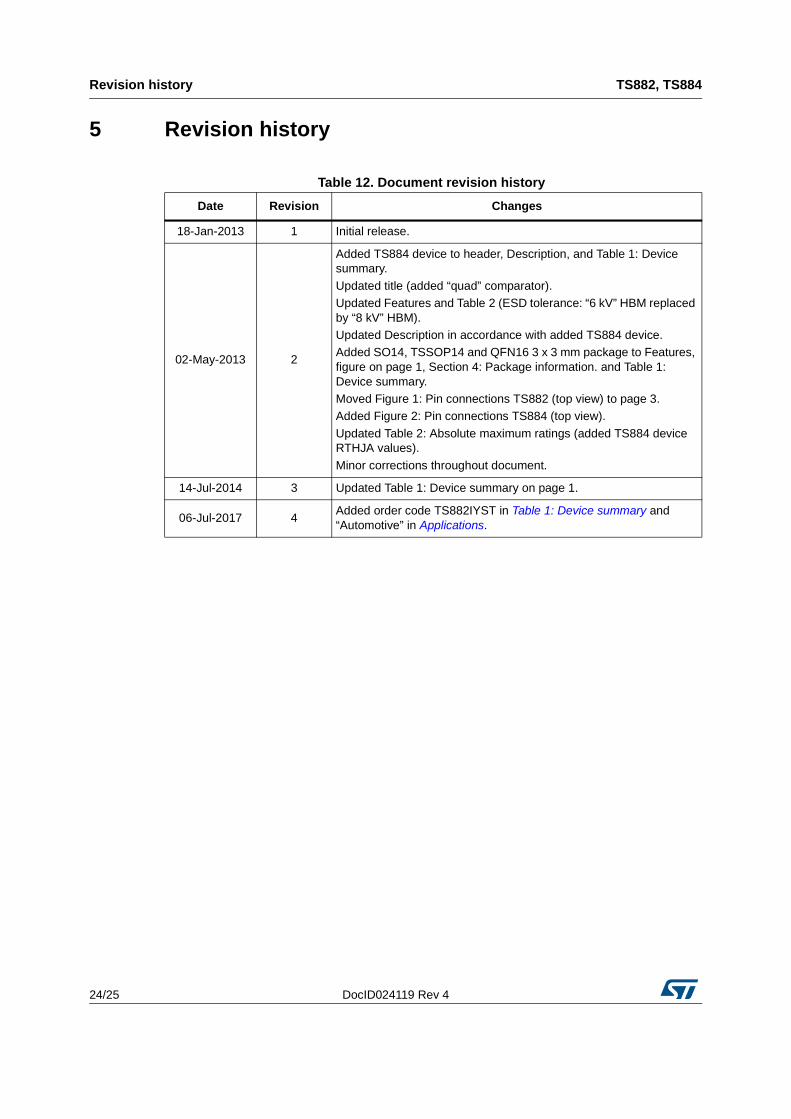
5 Revision history
Table 12. Document revision history
Date Revision Changes
18-Jan-2013 1 Initial release.
02-May-2013 2
Added TS884 device to header, Description, and Table 1: Device summary.
Updated title (added “quad” comparator).Updated Features and Table 2 (ESD tolerance: “6 kV” HBM replaced by “8 kV” HBM).Updated Description in accordance with added TS884 device.Added SO14, TSSOP14 and QFN16 3 x 3 mm package to Features, figure on page 1, Section 4: Package information. and Table 1: Device summary.Moved Figure 1: Pin connections TS882 (top view) to page 3.Added Figure 2: Pin connections TS884 (top view).
Updated Table 2: Absolute maximum ratings (added TS884 device RTHJA values).
Minor corrections throughout document.
14-Jul-2014 3 Updated Table 1: Device summary on page 1.
06-Jul-2017 4Added order code TS882IYST in Table 1: Device summary and “Automotive” in Applications.

DocID024119 Rev 4 25/25
TS882, TS884
25
IMPORTANT NOTICE – PLEASE READ CAREFULLY
STMicroelectronics NV and its subsidiaries (“ST”) reserve the right to make changes, corrections, enhancements, modifications, and improvements to ST products and/or to this document at any time without notice. Purchasers should obtain the latest relevant information on ST products before placing orders. ST products are sold pursuant to ST’s terms and conditions of sale in place at the time of order acknowledgement.
Purchasers are solely responsible for the choice, selection, and use of ST products and ST assumes no liability for application assistance or the design of Purchasers’ products.
No license, express or implied, to any intellectual property right is granted by ST herein.
Resale of ST products with provisions different from the information set forth herein shall void any warranty granted by ST for such product.
ST and the ST logo are trademarks of ST. All other product or service names are the property of their respective owners.
Information in this document supersedes and replaces information previously supplied in any prior versions of this document.
© 2017 STMicroelectronics – All rights reserved