rail-to-rail 1.8 v high-speed comparator
TRANSCRIPT
July 2016 DocID12485 Rev 8 1/20
This is information on a product in full production. www.st.com
TS3021, TS3021A
Rail-to-rail 1.8 V high-speed comparator
Datasheet - production data
Features Propagation delay: 38 ns
Low current consumption: 73 µA
Rail-to-rail inputs
Push-pull outputs
Supply operation from 1.8 to 5 V
Wide temperature range: -40 °C to 125 °C
High ESD tolerance: 5 kV HBM, 300 V MM
Latch-up immunity: 200 mA
SMD packages
Automotive qualification
Related products TS3022 for a dual comparator with similar
performances
TS3011 for a high-speed comparator
Applications Telecom
Instrumentation
Signal conditioning
High-speed sampling systems
Portable communication systems
Description The TS3021 single comparator features high-speed response time with rail-to-rail inputs. With a supply voltage specified from 2 to 5 V, this comparator can operate over a wide temperature range: -40 °C to 125 °C.
The TS3021 comparator offers micropower consumption as low as a few tens of microamperes thus providing an excellent ratio of power consumption current versus response time.
The TS3021 includes push-pull outputs and is available in small packages (SOT23-5 and SC70-5).
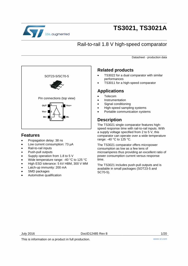
Pin connections (top view)
SOT23-5/SC70-5
5
4
OUT
Vcc-
1
2
IN+
Vcc+
3IN-
+ -
Contents TS3021, TS3021A
2/20 DocID12485 Rev 8
Contents
1 Absolute maximum ratings and operating conditions ................. 3
2 Electrical characteristics ................................................................ 4
3 Electrical characteristic curves .................................................... 10
4 Package information ..................................................................... 15
4.1 SOT23-5 package information ........................................................ 16
4.2 SC70-5 (or SOT323-5) package information ................................... 17
5 Ordering information ..................................................................... 18
6 Revision history ............................................................................ 19
TS3021, TS3021A Absolute maximum ratings and operating conditions
DocID12485 Rev 8 3/20
1 Absolute maximum ratings and operating conditions Table 1: Absolute maximum ratings (AMR)
Symbol Parameter Value Unit
VCC Supply voltage, VCC = (VCC+) - (VCC-) (1) 5.5
V VID Differential input voltage (2) ±5
VIN Input voltage range (VCC-) - 0.3 to (VCC+) + 0.3
Rthja Thermal resistance junction-to-ambient (3) SOT23-5 250
°C/W SC70-5 205
Rthjc Thermal resistance junction-to-case (3) SOT23-5 81
SC70-5 172
Tstg Storage temperature -65 to 150
°C Tj Junction temperature 150
TLEAD Lead temperature (soldering 10 s) 260
ESD
HBM: human body model (4) 5000
V MM: machine model (5) 300
CDM: charged device model (6) 1500
Latch-up immunity 200 mA
Notes:
(1)All voltage values, except the differential voltage are referenced to (VCC-) (2)The magnitude of the input and output voltages must never exceed the supply rail ±0.3 V (3)Short circuits can cause excessive heating. These values are typical (4)Human body model: a 100 pF capacitor is charged to the specified voltage, then discharged through a 1.5 kΩ resistor between two pins of the device. This is done for all couples of connected pin combinations while the other pins are floating. (5)Machine model: a 200 pF capacitor is charged to the specified voltage, then discharged directly between two pins of the device with no external series resistor (internal resistor < 5 Ω). This is done for all couples of connected pin combinations while the other pins are floating. (6)Charged device model: all pins and the package are charged together to the specified voltage and then discharged directly to the ground through only one pin. This is done for all pins.
Table 2: Operating conditions
Symbol Parameter Value Unit
VCC Supply voltage 0 °C < Tamb < 125 °C 1.8 to 5
V -40 °C < Tamb < 125°C 2 to 5
Vicm Common mode input
voltage range
-40 °C < Tamb < 85 °C (VCC- ) - 0.2 to (VCC+) + 0.2
85 °C < Tamb < 125 °C (VCC- ) to (VCC+)
Toper Operating temperature range -40 to 125 °C
Electrical characteristics TS3021, TS3021A
4/20 DocID12485 Rev 8
2 Electrical characteristics Table 3: Electrical characteristics at VCC = 2 V, Tamb = 25 ° C, and full Vicm range
(unless otherwise specified)
Symbol Parameter Test conditions (1) Min. Typ. Max. Unit
VIO Input offset voltage
TS3021A
0.5 2
mV TS3021
0.5 6
-40 °C < Tamb < 125 °C, TS3021A
4
-40 °C < Tamb < 125 °C, TS3021
7
ΔVio/ΔT Input offset voltage drift -40 °C < Tamb < 125 °C
3 20 µV/°C
IIO Input offset current (2) Tamb
1 20
nA -40 °C < Tamb < 125 °C
100
IIB Input bias current (2) Tamb
86 160
-40 °C < Tamb < 125 °C
300
ICC Supply current
No load, output high, Vicm = 0 V
73 90
µA
No load, output high, Vicm = 0 V,
-40 °C < Tamb < 125 °C 115
No load, output low, Vicm = 0 V
84 105
No load, output low, Vicm = 0 V,
-40 °C < Tamb < 125 °C 125
ISC Short-circuit current Source
9
mA Sink
10
VOH Output voltage high Isource = 1 mA 1.88 1.92
V -40 °C < Tamb < 125 °C 1.80
VOL Output voltage low Isink = 1 mA
60 100
mV -40 °C < Tamb < 125 °C
150
CMRR Common mode rejection
ratio 0 < Vicm < 2 V
67
dB
SVR Supply voltage rejection ∆Vcc = 2 to 5 V 58 73
TPLH Propagation delay, low to
high output level (3)
Vicm = 0 V, f = 10 kHz,
CL = 50 pF, overdrive = 100 mV 38 60
ns
Vicm = 0 V, f = 10 kHz,
CL = 50 pF, overdrive = 20 mV 48 75
TPHL Propagation delay, high to
low output level (4)
Vicm = 0 V, f = 10 kHz,
CL = 50 pF, overdrive = 100 mV 40 60
Vicm = 0 V, f = 10 kHz,
CL = 50 pF, overdrive = 20 mV 49 75
TF Fall time f = 10 kHz, CL = 50 pF,
RL = 10 kΩ, overdrive = 100 mV 8
TR Rise time f = 10 kHz, CL = 50 pF,
RL = 10 kΩ, overdrive = 100 mV 9

TS3021, TS3021A Electrical characteristics
DocID12485 Rev 8 5/20
Notes:
(1)All values over the temperature range are guaranteed through correlation and simulation. No production test is performed at the temperature range limits (2)Maximum values include unavoidable inaccuracies of the industrial tests (3)Response time is measured 10%/90% of the final output value with the following conditions: inverting input voltage (IN-) = Vicm and non-inverting input voltage (IN+) moving from Vicm - 100 mV to Vicm + overdrive. (4)Response time is measured 10%/90% of the final output value with the following conditions: Inverting input voltage (IN-) = Vicm and non-inverting input voltage (IN+) moving from Vicm + 100 mV to Vicm - overdrive.
Electrical characteristics TS3021, TS3021A
6/20 DocID12485 Rev 8
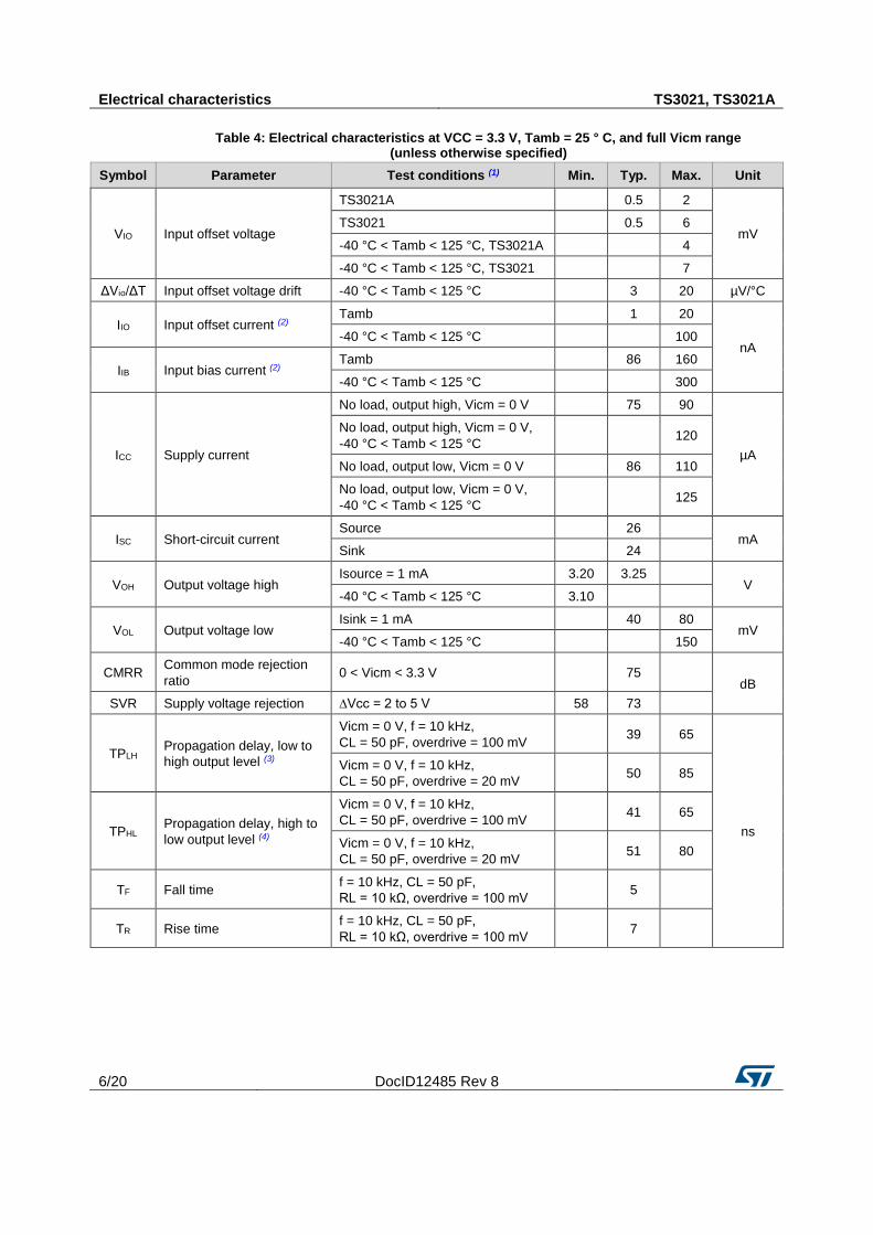
Table 4: Electrical characteristics at VCC = 3.3 V, Tamb = 25 ° C, and full Vicm range
(unless otherwise specified)
Symbol Parameter Test conditions (1) Min. Typ. Max. Unit
VIO Input offset voltage
TS3021A
0.5 2
mV TS3021
0.5 6
-40 °C < Tamb < 125 °C, TS3021A
4
-40 °C < Tamb < 125 °C, TS3021
7
ΔVio/ΔT Input offset voltage drift -40 °C < Tamb < 125 °C
3 20 µV/°C
IIO Input offset current (2) Tamb
1 20
nA -40 °C < Tamb < 125 °C
100
IIB Input bias current (2) Tamb
86 160
-40 °C < Tamb < 125 °C
300
ICC Supply current
No load, output high, Vicm = 0 V
75 90
µA
No load, output high, Vicm = 0 V,
-40 °C < Tamb < 125 °C 120
No load, output low, Vicm = 0 V
86 110
No load, output low, Vicm = 0 V,
-40 °C < Tamb < 125 °C 125
ISC Short-circuit current Source
26
mA Sink
24
VOH Output voltage high Isource = 1 mA 3.20 3.25
V -40 °C < Tamb < 125 °C 3.10
VOL Output voltage low Isink = 1 mA
40 80
mV -40 °C < Tamb < 125 °C
150
CMRR Common mode rejection
ratio 0 < Vicm < 3.3 V
75
dB
SVR Supply voltage rejection ∆Vcc = 2 to 5 V 58 73
TPLH Propagation delay, low to
high output level (3)
Vicm = 0 V, f = 10 kHz,
CL = 50 pF, overdrive = 100 mV 39 65
ns
Vicm = 0 V, f = 10 kHz,
CL = 50 pF, overdrive = 20 mV 50 85
TPHL Propagation delay, high to
low output level (4)
Vicm = 0 V, f = 10 kHz,
CL = 50 pF, overdrive = 100 mV 41 65
Vicm = 0 V, f = 10 kHz,
CL = 50 pF, overdrive = 20 mV 51 80
TF Fall time f = 10 kHz, CL = 50 pF,
RL = 10 kΩ, overdrive = 100 mV 5
TR Rise time f = 10 kHz, CL = 50 pF,
RL = 10 kΩ, overdrive = 100 mV 7

TS3021, TS3021A Electrical characteristics
DocID12485 Rev 8 7/20
Notes:
(1)All values over the temperature range are guaranteed through correlation and simulation. No production test is performed at the temperature range limits (2)Maximum values include unavoidable inaccuracies of the industrial tests (3)Response time is measured 10%/90% of the final output value with the following conditions: inverting input voltage (IN-) = Vicm and non-inverting input voltage (IN+) moving from Vicm - 100 mV to Vicm + overdrive. (4)Response time is measured 10%/90% of the final output value with the following conditions: Inverting input voltage (IN-) = Vicm and non-inverting input voltage (IN+) moving from Vicm + 100 mV to Vicm - overdrive.
Electrical characteristics TS3021, TS3021A
8/20 DocID12485 Rev 8
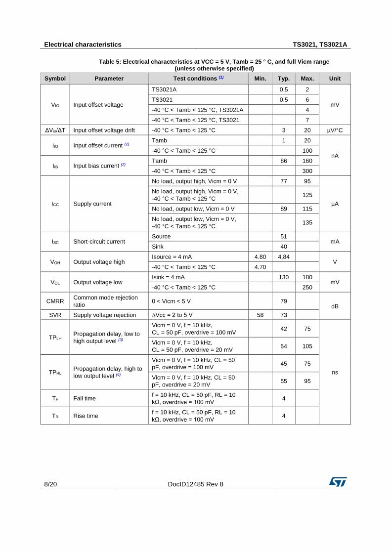
Table 5: Electrical characteristics at VCC = 5 V, Tamb = 25 ° C, and full Vicm range
(unless otherwise specified)
Symbol Parameter Test conditions (1) Min. Typ. Max. Unit
VIO Input offset voltage
TS3021A
0.5 2
mV TS3021
0.5 6
-40 °C < Tamb < 125 °C, TS3021A
4
-40 °C < Tamb < 125 °C, TS3021
7
ΔVio/ΔT Input offset voltage drift -40 °C < Tamb < 125 °C
3 20 µV/°C
IIO Input offset current (2) Tamb
1 20
nA -40 °C < Tamb < 125 °C
100
IIB Input bias current (2) Tamb
86 160
-40 °C < Tamb < 125 °C
300
ICC Supply current
No load, output high, Vicm = 0 V
77 95
µA
No load, output high, Vicm = 0 V,
-40 °C < Tamb < 125 °C 125
No load, output low, Vicm = 0 V
89 115
No load, output low, Vicm = 0 V,
-40 °C < Tamb < 125 °C 135
ISC Short-circuit current Source
51
mA Sink
40
VOH Output voltage high Isource = 4 mA 4.80 4.84
V -40 °C < Tamb < 125 °C 4.70
VOL Output voltage low Isink = 4 mA
130 180
mV -40 °C < Tamb < 125 °C
250
CMRR Common mode rejection
ratio 0 < Vicm < 5 V
79
dB
SVR Supply voltage rejection ∆Vcc = 2 to 5 V 58 73
TPLH Propagation delay, low to
high output level (3)
Vicm = 0 V, f = 10 kHz,
CL = 50 pF, overdrive = 100 mV 42 75
ns
Vicm = 0 V, f = 10 kHz,
CL = 50 pF, overdrive = 20 mV 54 105
TPHL Propagation delay, high to
low output level (4)
Vicm = 0 V, f = 10 kHz, CL = 50
pF, overdrive = 100 mV 45 75
Vicm = 0 V, f = 10 kHz, CL = 50
pF, overdrive = 20 mV 55 95
TF Fall time f = 10 kHz, CL = 50 pF, RL = 10
kΩ, overdrive = 100 mV 4
TR Rise time f = 10 kHz, CL = 50 pF, RL = 10
kΩ, overdrive = 100 mV 4
TS3021, TS3021A Electrical characteristics
DocID12485 Rev 8 9/20
Notes:
(1)All values over the temperature range are guaranteed through correlation and simulation. No production test is performed at the temperature range limits (2)Maximum values include unavoidable inaccuracies of the industrial tests (3)Response time is measured 10%/90% of the final output value with the following conditions: inverting input voltage (IN-) = Vicm and non-inverting input voltage (IN+) moving from Vicm - 100 mV to Vicm + overdrive. (4)Response time is measured 10%/90% of the final output value with the following conditions: Inverting input voltage (IN-) = Vicm and non-inverting input voltage (IN+) moving from Vicm + 100 mV to Vicm - overdrive.
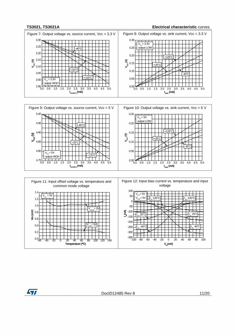
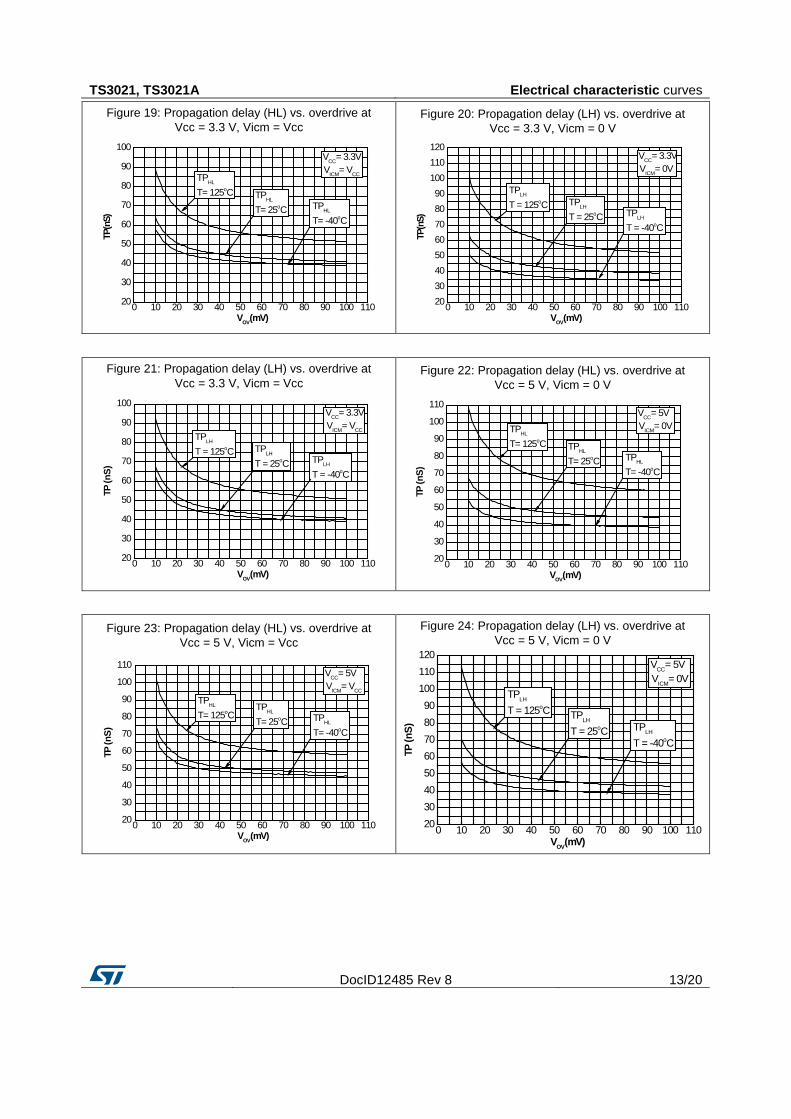
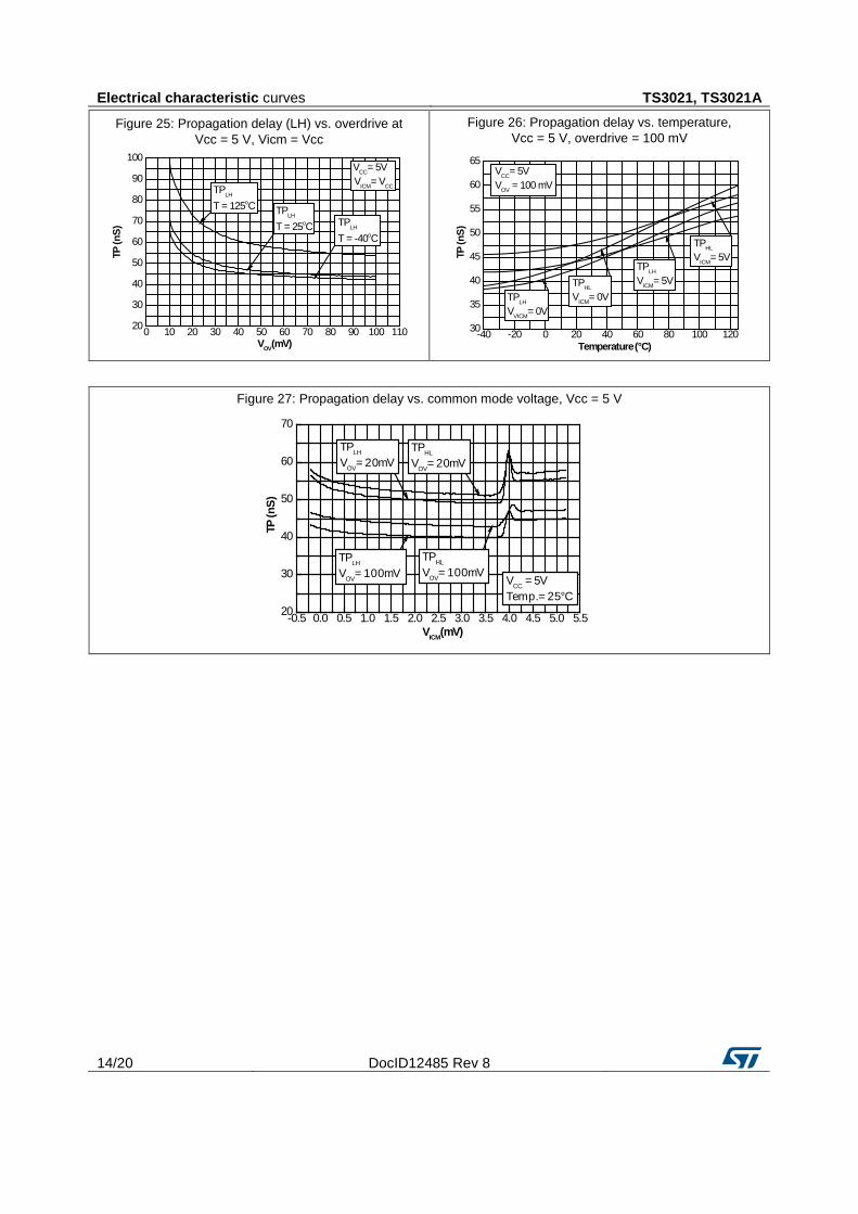
Electrical characteristic curves TS3021, TS3021A
10/20 DocID12485 Rev 8
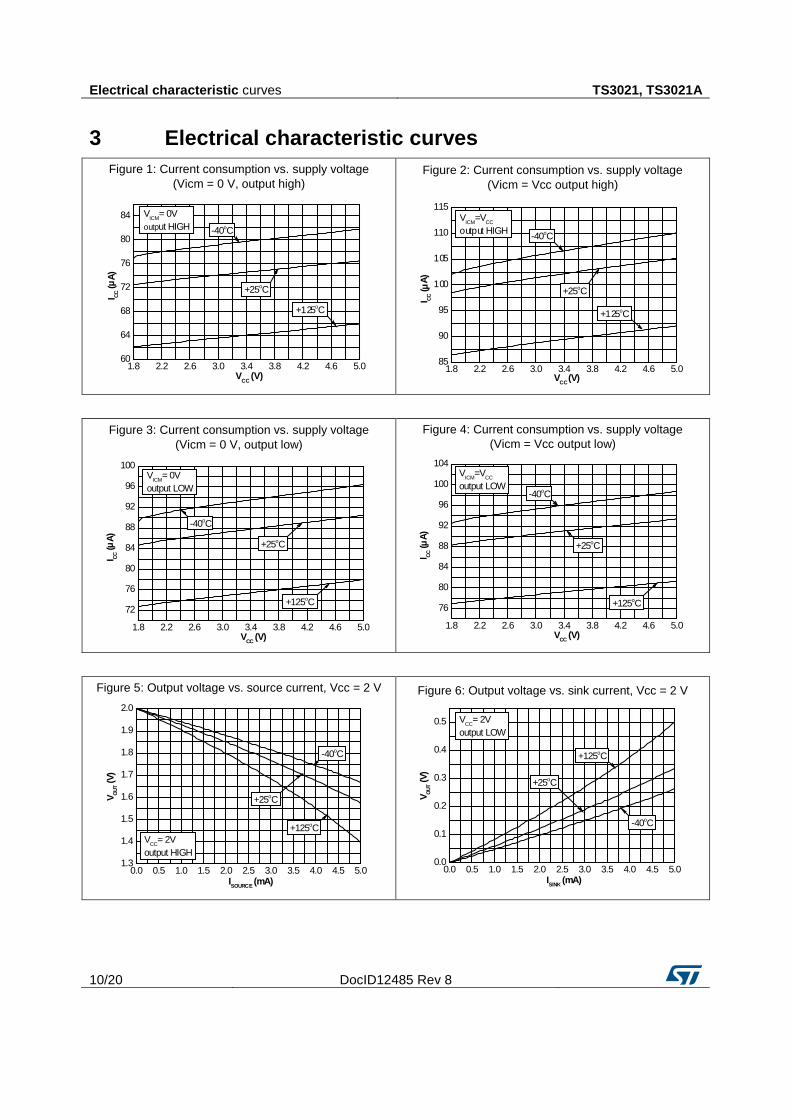
3 Electrical characteristic curves
Figure 1: Current consumption vs. supply voltage
(Vicm = 0 V, output high)
Figure 2: Current consumption vs. supply voltage
(Vicm = Vcc output high)
Figure 3: Current consumption vs. supply voltage
(Vicm = 0 V, output low)
Figure 4: Current consumption vs. supply voltage
(Vicm = Vcc output low)
Figure 5: Output voltage vs. source current, Vcc = 2 V
Figure 6: Output voltage vs. sink current, Vcc = 2 V
1.8 2.2 2.6 3.0 3.4 3.8 4.2 4.6 5.060
64
68
72
76
80
84
I CC
(A
)
VCC
(V)
-40oC
+125oC
+25oC
VICM
= 0V
output HIGH
µ
1.8 2.2 2.6 3.0 3.4 3.8 4.2 4.6 5.085
90
95
100
105
110
115
I CC
(A
)
VCC
(V)
-40oC
+125oC
+25oC
VICM
=VCC
output HIGH
µ
1.8 2.2 2.6 3.0 3.4 3.8 4.2 4.6 5.0
72
76
80
84
88
92
96
100
I CC
(A
)
VCC
(V)
-40oC
+125oC
+25oC
VICM
= 0V
output LOW
µ
1.8 2.2 2.6 3.0 3.4 3.8 4.2 4.6 5.0
76
80
84
88
92
96
100
104
I CC
(A
)
VCC
(V)
-40oC
+125oC
+25oC
VICM
=VCC
output LOW
µ
0.0 0.5 1.0 1.5 2.0 2.5 3.0 3.5 4.0 4.5 5.01.3
1.4
1.5
1.6
1.7
1.8
1.9
2.0
VO
UT(V
)
ISOURCE
(mA)
+125oC
-40oC
+25oC
VCC
= 2V
output HIGH
0.0 0.5 1.0 1.5 2.0 2.5 3.0 3.5 4.0 4.5 5.00.0
0.1
0.2
0.3
0.4
0.5
+25oC
VO
UT(V
)
ISINK
(mA)
+125oC
-40oC
VCC
= 2V
output LOW
TS3021, TS3021A Electrical characteristic curves
DocID12485 Rev 8 11/20
Figure 7: Output voltage vs. source current, Vcc = 3.3 V
Figure 8: Output voltage vs. sink current, Vcc = 3.3 V
Figure 9: Output voltage vs. source current, Vcc = 5 V
Figure 10: Output voltage vs. sink current, Vcc = 5 V
Figure 11: Input offset voltage vs. temperature and
common mode voltage
Figure 12: Input bias current vs. temperature and input
voltage
0.0 0.5 1.0 1.5 2.0 2.5 3.0 3.5 4.0 4.5 5.02.95
3.00
3.05
3.10
3.15
3.20
3.25
3.30
VO
UT(V
)
ISOURCE
(mA)
+125oC
-40oC
+25oC
VCC
= 3.3V
output HIGH
0.0 0.5 1.0 1.5 2.0 2.5 3.0 3.5 4.0 4.5 5.00.00
0.05
0.10
0.15
0.20
0.25
0.30
VO
UT(V
)
ISINK
(mA)
+125oC
-40oC
+25oC
VCC
= 3.3V
output LOW
0.0 0.5 1.0 1.5 2.0 2.5 3.0 3.5 4.0 4.5 5.04.75
4.80
4.85
4.90
4.95
5.00
VO
UT(V
)
ISOURCE
(mA)
+125oC
-40oC
+25oC
VCC
= 5V
output HIGH
0.0 0.5 1.0 1.5 2.0 2.5 3.0 3.5 4.0 4.5 5.00.00
0.05
0.10
0.15
0.20
0.25
VO
UT(V
)
ISINK
(mA)
+125oC
-40oC
+25oC
VCC
= 5V
output LOW
-60 -40 -20 0 20 40 60 80 100 120 1400.0
0.2
0.4
0.6
0.8
1.0
1.2
1.4
Vio
(m
V)
Temperature ( C)
VVICM
= 0V
VICM
= 5V
VCC
= 5V
-100 -80 -60 -40 -20 0 20 40 60 80 100-350
-300
-250
-200
-150
-100
-50
0
50
100
IIN+
125oCI
IN-125
oC
IIN-
25oCI
IN+25
oC
IIN-
-40oCI
IN+-40
oC
I IB(n
A)
VIN(mV)
VCC
= 5V
VICM
= 0V
Electrical characteristic curves TS3021, TS3021A
12/20 DocID12485 Rev 8
Figure 13: Current consumption vs. commutation
frequency
Figure 14: Propagation delay (HL) vs. overdrive at
Vcc = 2 V, Vicm = 0 V
Figure 15: Propagation delay (HL) vs. overdrive at
Vcc = 2 V, Vicm = Vcc
Figure 16: Propagation delay (LH) vs. overdrive at
Vcc = 2 V, Vicm = 0 V
Figure 17: Propagation delay (LH) vs. overdrive at
Vcc = 2 V, Vicm = Vcc
Figure 18: Propagation delay (HL) vs. overdrive at
Vcc = 3.3 V, Vicm = 0 V
10k 100k 1M0
100
200
300
400
500
600
VCC
= 2V
VCC
= 3.3V
I CC
Frequency (Hz)
VCC
= 5V
VICM
= 0V
CLOAD
= 50pF
(µA
)
0 10 20 30 40 50 60 70 80 90 100 11020
30
40
50
60
70
80
90
100
TP
(nS
)
VOV
(mV)
TPHL
T= -40oC
TPHL
T= 125oC
TPHL
T= 25oC
VCC
= 2V
VICM
= 0V
0 10 20 30 40 50 60 70 80 90 100 11020
30
40
50
60
70
80
90
100
TP
(n
S)
VOV
(mV)
TPHL
T= -40oC
TPHL
T= 125oC TP
HL
T= 25oC
VCC
= 2V
VICM
= VCC
0 10 20 30 40 50 60 70 80 90 100 11020
30
40
50
60
70
80
90
100
TP
(n
S)
VOV
(mV)
TPLH
T= -40oC
TPLH
T= 125oC
TPLH
T= 25oC
VCC
= 2V
VICM
= 0V
0 10 20 30 40 50 60 70 80 90 100 11020
30
40
50
60
70
80
90
100
TP
(n
S)
VOV
(mV)
TPLH
T= -40oC
TPLH
T= 125oC TP
LH
T= 25oC
VCC
= 2V
VICM
= VCC
0 10 20 30 40 50 60 70 80 90 100 11020
30
40
50
60
70
80
90
100
TP
(n
S)
VOV
(mV)
TPHL
T= -40oC
TPHL
T= 125oC TP
HL
T= 25oC
VCC
= 3.3V
VICM
= 0V
TS3021, TS3021A Electrical characteristic curves
DocID12485 Rev 8 13/20
Figure 19: Propagation delay (HL) vs. overdrive at
Vcc = 3.3 V, Vicm = Vcc
Figure 20: Propagation delay (LH) vs. overdrive at
Vcc = 3.3 V, Vicm = 0 V
Figure 21: Propagation delay (LH) vs. overdrive at
Vcc = 3.3 V, Vicm = Vcc
Figure 22: Propagation delay (HL) vs. overdrive at
Vcc = 5 V, Vicm = 0 V
Figure 23: Propagation delay (HL) vs. overdrive at
Vcc = 5 V, Vicm = Vcc
Figure 24: Propagation delay (LH) vs. overdrive at
Vcc = 5 V, Vicm = 0 V
0 10 20 30 40 50 60 70 80 90 100 11020
30
40
50
60
70
80
90
100
TP
(nS
)
VOV
(mV)
TPHL
T= -40oC
TPHL
T= 125oC TP
HL
T= 25oC
VCC
= 3.3V
VICM
= VCC
0 10 20 30 40 50 60 70 80 90 100 11020
30
40
50
60
70
80
90
100
110
120
TP
(nS
)
VOV
(mV)
TPLH
T = -40oC
TPLH
T = 125oC TP
LH
T = 25oC
VCC
= 3.3V
VICM
= 0V
0 10 20 30 40 50 60 70 80 90 100 11020
30
40
50
60
70
80
90
100
TP
(n
S)
VOV
(mV)
TPLH
T = -40oC
TPLH
T = 125oC TP
LH
T = 25oC
VCC
= 3.3V
VICM
= VCC
0 10 20 30 40 50 60 70 80 90 100 11020
30
40
50
60
70
80
90
100
110
TP
(n
S)
VOV
(mV)
TPHL
T= -40oC
TPHL
T= 125oC TP
HL
T= 25oC
VCC
= 5V
VICM
= 0V
0 10 20 30 40 50 60 70 80 90 100 11020
30
40
50
60
70
80
90
100
110
TP
(n
S)
VOV
(mV)
TPHL
T= -40oC
TPHL
T= 125oC
TPHL
T= 25oC
VCC
= 5V
VICM
= VCC
0 10 20 30 40 50 60 70 80 90 100 11020
30
40
50
60
70
80
90
100
110
120
TP
(n
S)
VOV
(mV)
TPLH
T = -40oC
TPLH
T = 125oC TP
LH
T = 25oC
VCC
= 5V
VICM
= 0V
Electrical characteristic curves TS3021, TS3021A
14/20 DocID12485 Rev 8
Figure 25: Propagation delay (LH) vs. overdrive at
Vcc = 5 V, Vicm = Vcc
Figure 26: Propagation delay vs. temperature,
Vcc = 5 V, overdrive = 100 mV
Figure 27: Propagation delay vs. common mode voltage, Vcc = 5 V
0 10 20 30 40 50 60 70 80 90 100 11020
30
40
50
60
70
80
90
100
TP
(n
S)
VOV
(mV)
TPLH
T = -40oC
TPLH
T = 125oC TP
LH
T = 25oC
VCC
= 5V
VICM
= VCC
-40 -20 0 20 40 60 80 100 12030
35
40
45
50
55
60
65
TPHL
VICM
= 5VTP
(n
S)
Temperature(°C)
TPLH
VVICM
= 0V
TPHL
VICM
= 0V
TPLH
VICM
= 5V
VCC
= 5V
VOV
= 100 mV
-0.5 0.0 0.5 1.0 1.5 2.0 2.5 3.0 3.5 4.0 4.5 5.0 5.520
30
40
50
60
70
TPHL
VOV
= 20mV
TP
(n
S)
VICM
(mV)
TPLH
VOV
= 20mV
TPLH
VOV
= 100mV
TPHL
VOV
= 100mVV
CC= 5V
Temp.= 25°C
TS3021, TS3021A Package information
DocID12485 Rev 8 15/20
4 Package information
In order to meet environmental requirements, ST offers these devices in different grades of ECOPACK® packages, depending on their level of environmental compliance. ECOPACK® specifications, grade definitions and product status are available at: www.st.com. ECOPACK® is an ST trademark.
Package information TS3021, TS3021A
16/20 DocID12485 Rev 8
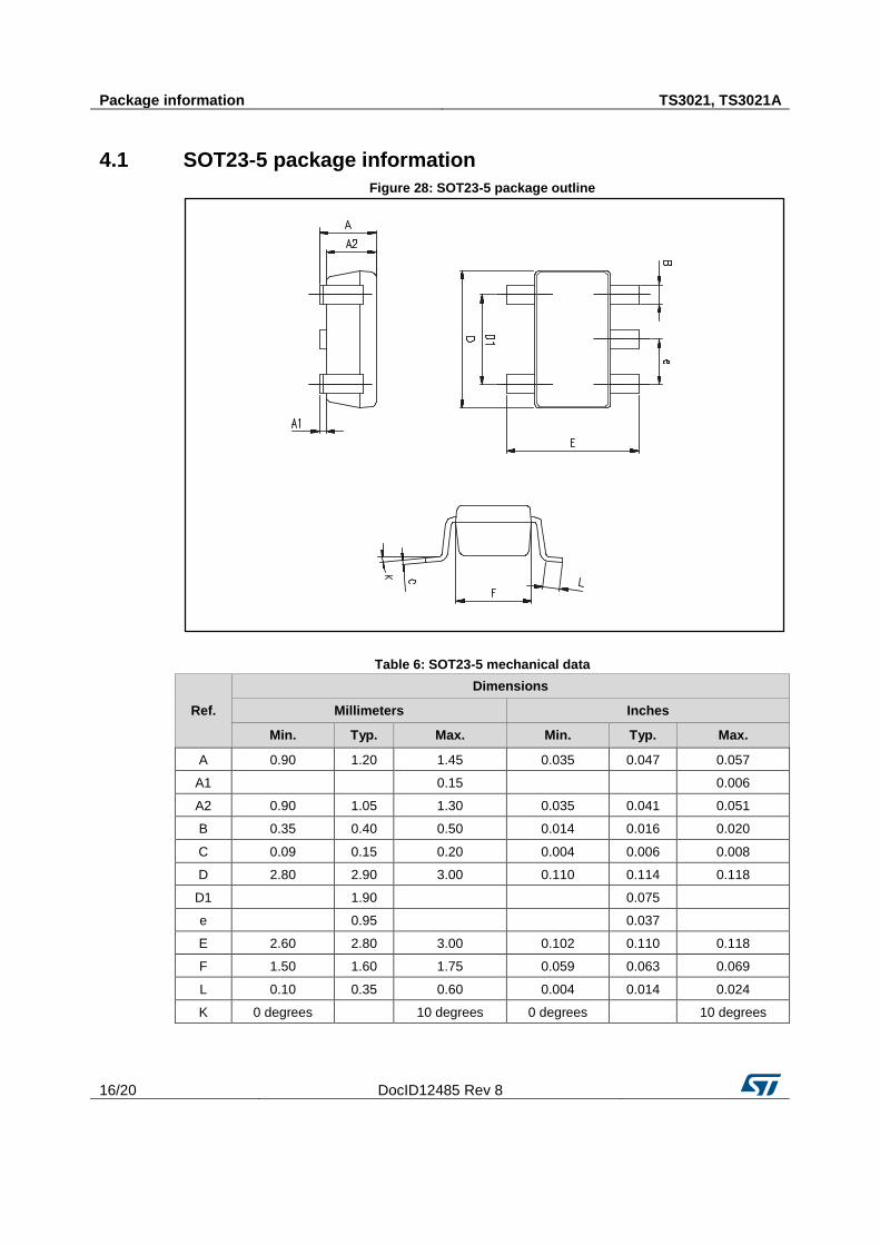
4.1 SOT23-5 package information
Figure 28: SOT23-5 package outline
Table 6: SOT23-5 mechanical data
Ref.
Dimensions
Millimeters Inches
Min. Typ. Max. Min. Typ. Max.
A 0.90 1.20 1.45 0.035 0.047 0.057
A1
0.15
0.006
A2 0.90 1.05 1.30 0.035 0.041 0.051
B 0.35 0.40 0.50 0.014 0.016 0.020
C 0.09 0.15 0.20 0.004 0.006 0.008
D 2.80 2.90 3.00 0.110 0.114 0.118
D1
1.90
0.075
e
0.95
0.037
E 2.60 2.80 3.00 0.102 0.110 0.118
F 1.50 1.60 1.75 0.059 0.063 0.069
L 0.10 0.35 0.60 0.004 0.014 0.024
K 0 degrees
10 degrees 0 degrees
10 degrees
TS3021, TS3021A Package information
DocID12485 Rev 8 17/20
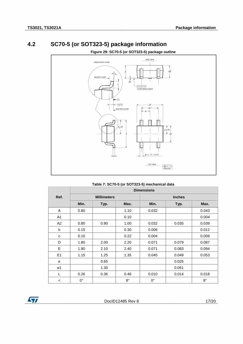
4.2 SC70-5 (or SOT323-5) package information
Figure 29: SC70-5 (or SOT323-5) package outline
Table 7: SC70-5 (or SOT323-5) mechanical data
Ref.
Dimensions
Millimeters Inches
Min. Typ. Max. Min. Typ. Max.
A 0.80
1.10 0.032
0.043
A1
0.10
0.004
A2 0.80 0.90 1.00 0.032 0.035 0.039
b 0.15
0.30 0.006
0.012
c 0.10
0.22 0.004
0.009
D 1.80 2.00 2.20 0.071 0.079 0.087
E 1.80 2.10 2.40 0.071 0.083 0.094
E1 1.15 1.25 1.35 0.045 0.049 0.053
e
0.65
0.025
e1
1.30
0.051
L 0.26 0.36 0.46 0.010 0.014 0.018
< 0°
8° 0°
8°
SEATING PLANE
GAUGE PLANE
DIMENSIONS IN MM
SIDE VIEW
TOP VIEW
COPLANAR LEADS
Ordering information TS3021, TS3021A
18/20 DocID12485 Rev 8
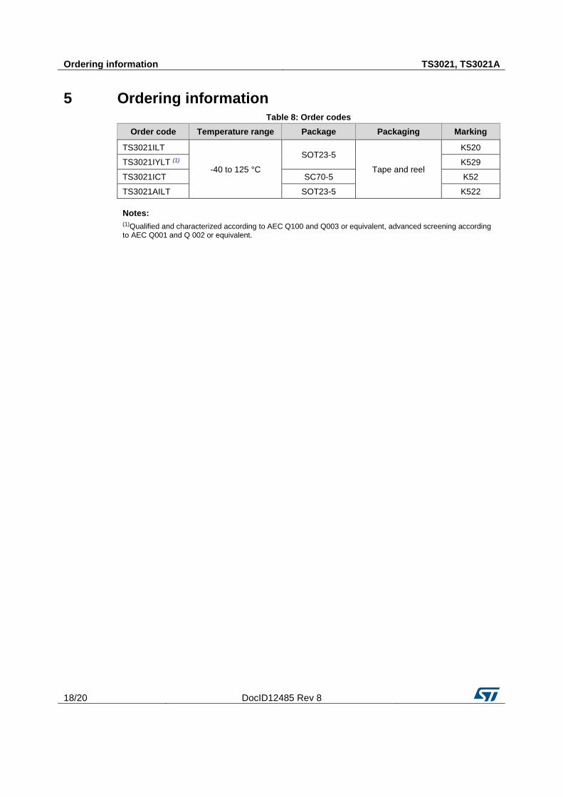
5 Ordering information Table 8: Order codes
Order code Temperature range Package Packaging Marking
TS3021ILT
-40 to 125 °C
SOT23-5
Tape and reel
K520
TS3021IYLT (1) K529
TS3021ICT SC70-5 K52
TS3021AILT SOT23-5 K522
Notes:
(1)Qualified and characterized according to AEC Q100 and Q003 or equivalent, advanced screening according to AEC Q001 and Q 002 or equivalent.
TS3021, TS3021A Revision history
DocID12485 Rev 8 19/20
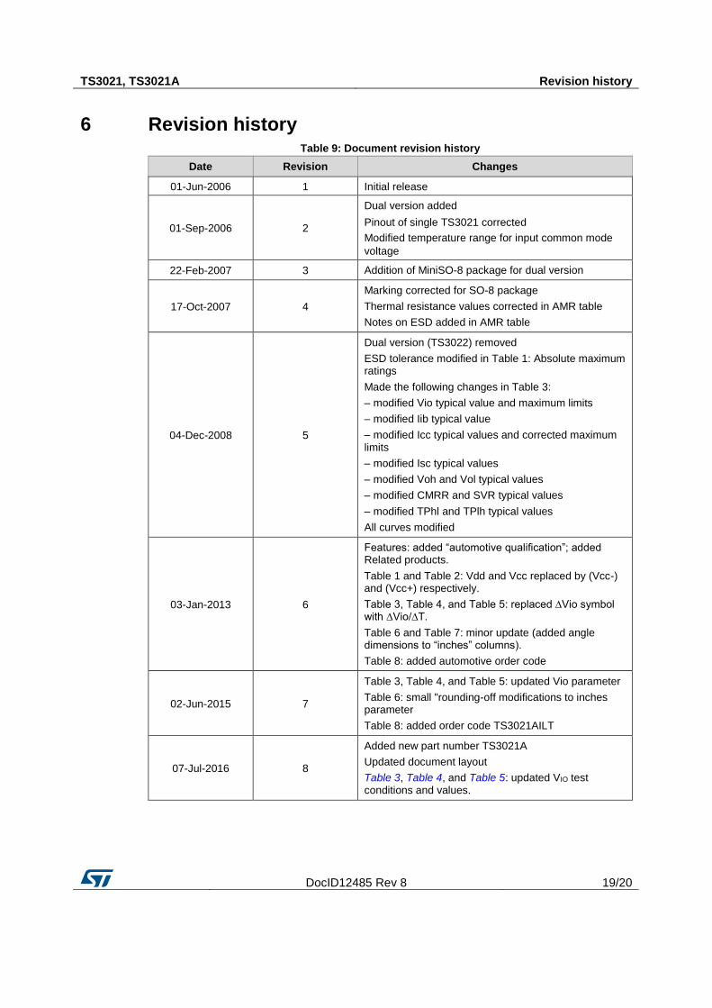
6 Revision history Table 9: Document revision history
Date Revision Changes
01-Jun-2006 1 Initial release
01-Sep-2006 2
Dual version added
Pinout of single TS3021 corrected
Modified temperature range for input common mode
voltage
22-Feb-2007 3 Addition of MiniSO-8 package for dual version
17-Oct-2007 4
Marking corrected for SO-8 package
Thermal resistance values corrected in AMR table
Notes on ESD added in AMR table
04-Dec-2008 5
Dual version (TS3022) removed
ESD tolerance modified in Table 1: Absolute maximum ratings
Made the following changes in Table 3:
– modified Vio typical value and maximum limits
– modified Iib typical value
– modified Icc typical values and corrected maximum limits
– modified Isc typical values
– modified Voh and Vol typical values
– modified CMRR and SVR typical values
– modified TPhl and TPlh typical values
All curves modified
03-Jan-2013 6
Features: added “automotive qualification”; added Related products.
Table 1 and Table 2: Vdd and Vcc replaced by (Vcc-) and (Vcc+) respectively.
Table 3, Table 4, and Table 5: replaced ∆Vio symbol with ∆Vio/∆T.
Table 6 and Table 7: minor update (added angle dimensions to “inches” columns).
Table 8: added automotive order code
02-Jun-2015 7
Table 3, Table 4, and Table 5: updated Vio parameter
Table 6: small "rounding-off modifications to inches parameter
Table 8: added order code TS3021AILT
07-Jul-2016 8
Added new part number TS3021A
Updated document layout
Table 3, Table 4, and Table 5: updated VIO test conditions and values.
TS3021, TS3021A
20/20 DocID12485 Rev 8
IMPORTANT NOTICE – PLEASE READ CAREFULLY
STMicroelectronics NV and its subsidiaries (“ST”) reserve the right to make changes, corrections, enhancements, modifications , and improvements to ST products and/or to this document at any time without notice. Purchasers should obtain the latest relevant information on ST products before placing orders. ST products are sold pursuant to ST’s terms and conditions of sale in place at the time of order acknowledgement.
Purchasers are solely responsible for the choice, selection, and use of ST products and ST assumes no liability for application assistance or the design of Purchasers’ products.
No license, express or implied, to any intellectual property right is granted by ST herein.
Resale of ST products with provisions different from the information set forth herein shall void any warranty granted by ST for such product.
ST and the ST logo are trademarks of ST. All other product or service names are the property of their respective owners.
Information in this document supersedes and replaces information previously supplied in any prior versions of this document.
© 2016 STMicroelectronics – All rights reserved