rail-to-rail i/o, 2a power amplifier (rev. a)rail-to-rail i/o, 2a power amplifier description ... rl...
TRANSCRIPT

OPA567
OPA567
Rail-to-Rail I/O, 2APOWER AMPLIFIER
DESCRIPTIONThe OPA567 is a low-cost, high-current, operational amplifierdesigned for driving a wide variety of loads while operating onlow-voltage supplies. It operates from either single or dualsupplies for design flexibility and has rail-to-rail swing on theinput and output. Output swing is within 300mV of the supplyrails, with output current of 2A. Smaller loads allow an outputswing closer to the rails.
The OPA567 is unity gain stable, easy to use, and free fromthe phase inversion problems found in some power amplifi-ers. High performance is maintained at voltage swings nearthe output rails.
The OPA567 provides an accurate user-selected currentlimit set with an external resistor, or digitally adjusted via aDigital-to-Analog Converter (DAC).
The output of the OPA567 can be independently disabledusing the Enable pin. This feature saves power and protectsthe load.
Two flags are provided. The current limit flag, IFLAG, warns ofcurrent limit conditions. TFLAG is a thermal flag that warns ofthermal overstress. The TFLAG pin can be connected to theEnable pin to provide a thermal shutdown solution.
The OPA567 is available in a tiny 5mm x 5mm QuadFlatpack No-lead (QFN) package and features an exposedthermal pad that enhances thermal and electrical character-istics. It is small and easy to heat sink. The OPA567 isspecified for operation over the industrial temperature range,–40°C to +85°C.
FEATURES HIGH OUTPUT CURRENT: 2A
OUTPUT SWINGS TO: 150mV of Rails with IO = 2A
THERMAL PROTECTION
ADJUSTABLE CURRENT LIMIT
TWO FLAGS: Current Limit and TemperatureWarning
LOW SUPPLY VOLTAGE OPERATION: 2.7V to 5.5V
SHUTDOWN FUNCTION WITH OUTPUT DISABLE
SMALL POWER PACKAGE
APPLICATIONS THERMOELECTRIC COOLER DRIVER
LASER DIODE PUMP DRIVER
VALVE, ACTUATOR DRIVER
SYNCHRO, SERVO DRIVER
TRANSDUCER EXCITATION
GENERAL LINEAR POWER BOOSTER FOROP AMPS
www.ti.com
Copyright © 2005, Texas Instruments Incorporated
SBOS287A – JUNE 2005 – REVISED SEPTEMBER 2005
OPA567
TFLAG
V–
VO
NOTE: (1) Connectfor thermal protection.
–IN
+IN
V+
8
1, 12
4, 5
10
117
2, 3
69
RSET
(1)
Enable
ISET
IFLAG
Please be aware that an important notice concerning availability, standard warranty, and use in critical applications ofTexas Instruments semiconductor products and disclaimers thereto appears at the end of this data sheet.
PowerPAD is a trademark of Texas Instruments. All other trademarks are the property of their respective owners.
OPA567 RELATED PRODUCTS
FEATURES PRODUCT
Same features as the OPA567, plus current OPA569monitor output and paralleling ability in SO-20PowerPAD™ package.
PRODUCTION DATA information is current as of publication date.Products conform to specifications per the terms of Texas Instrumentsstandard warranty. Production processing does not necessarily includetesting of all parameters.

OPA567SBOS287A
2www.ti.com
PIN # NAME DESCRIPTION
1, 12 V+ Positive Power-Supply Voltage
2, 3 VO Output
4, 5 V– Negative Power-Supply Voltage
6 ISET Current Limit Set Pin(1)
7 IFLAG Current Limit Flag—Indicates when part is incurrent limit (active LOW).
8 –IN Inverting Input
9 +IN Noninverting Input
10 TFLAG Thermal Flag—Indicates thermal stress (activeLOW).
11 ENABLE Enabled HIGH, shut down LOW.
ELECTROSTATICDISCHARGE SENSITIVITY
This integrated circuit can be damaged by ESD. TexasInstruments recommends that all integrated circuits be handledwith appropriate precautions. Failure to observe proper han-dling and installation procedures can cause damage.
ESD damage can range from subtle performance degrada-tion to complete device failure. Precision integrated circuitsmay be more susceptible to damage because very smallparametric changes could cause the device not to meet itspublished specifications.
Supply Voltage ................................................................................. +7.5VOutput Current ............................................................... See SOA CurvesSignal Input Terminals (pins 8 and 9):
Voltage(2) ............................................... (V–) – 0.5V to (V+) + 0.5VCurrent(2) ................................................................................ ±10mA
Output Short-Circuit(3) ........ Continuous when thermal protection enabledEnable Pin (pin 11) ........................................ (V–) – 0.5V to (V–) + 7.5VCurrent Limit Set, ILIMIT Pin (pin 6) ................ (V–) – 0.5V to (V+) + 0.5VOperating Temperature .................................................. –55°C to +125°CStorage Temperature ..................................................... –65°C to +150°CJunction Temperature .................................................................... +150°CESD Rating:
Human Body Model ................................................................... 3kVCharged Device Model .......................................................... 1500V
NOTES: (1) Stresses above these ratings may cause permanent damage.Exposure to absolute maximum conditions for extended periods may de-grade device reliability. These are stress ratings only, and functional opera-tion of the device at these or any other conditions beyond those specified isnot implied. (2) Input terminals are diode-clamped to the power-supply rails.Input signals that can swing more than 0.5V beyond the supply rails shouldbe current limited to 10mA or less. (3) Short-circuit to ground.
PIN CONFIGURATION
ABSOLUTE MAXIMUM RATINGS(1)
V+
VO
VO
+IN
–IN
IFLAG
1
2
3
9
8
7
Metalheat sink(located
on bottom)
V+
Ena
ble
TF
LAG
12 11 10
V–
V–
I SE
T
4 5 6
Top View QFN
PIN DESCRIPTIONS
NOTE: (1) This pin limits the output current. The limited value, ILIMIT, is9800(ISET), where ISET is the current flowing through the ISET pin. This currentis programmed by the resistor RSET connected to V–.
PACKAGE/ORDERING INFORMATIONFor the most current package and ordering information, seethe Package Option Addendum located at the end of thisdata sheet.

OPA567SBOS287A
3www.ti.com
ELECTRICAL CHARACTERISTICS: VS = +2.7V to +5.5VBoldface limits apply over the specified temperature range, TA = –40°C to +85°C.At TCASE = +25°C, RL = 1kΩ, and connected to VS/2, unless otherwise noted.
NOTES:(1) See typical characteristic, Maximum Output Voltage vs Frequency.(2) See typical characteristic, Total Harmonic Distortion + Noise vs Frequency.(3) Swing to the rail is measured in final test. Under those conditions, the AOL is derived from characterization.(4) See Safe Operating Area (SOA) plots.(5) See typical characteristic, Overshoot vs Load Capacitance.(6) See the Typical Characteristics section. Higher frequency output impedance can affect frequency stability.(7) External current limit setting resistor is required; see Figure 1.(8) ILIMIT is the value of the desired current limit and is equal to 9800(ISET), where ISET is the current through the ISET pin. ILIMIT tolerance is proportional to the ratio of
ILIMIT/ISET. Errors from this parameter can be calibrated out—see the Applications Information section.(9) VSET is a voltage reference that equals the difference between the voltage of the ISET pin and V–, and is referenced to the negative rail. Errors from this parameter
can be calibrated out—see the Applications Information section.
OPA567
PARAMETER CONDITION MIN TYP MAX UNITS
OFFSET VOLTAGEInput Offset Voltage VOS IO = 0V, VS = +5V ±0.5 ±2 mV
vs Temperature dVOS /dT TA = –40°C to +85°C ±1.3 µV/°Cvs Power Supply PSRR VS = +2.7V to +5.5V, VCM = (V–) +0.55V 12 60 µV/V
INPUT BIAS CURRENTInput Bias Current IB ±1 ±10 pA
vs Temperature (doubles every 10°C)Input Offset Current IOS ±2 ±10 pA
NOISEInput Voltage Noise Density, f = 1kHz en 12 nV/√Hz
f = 0.1Hz to 10Hz 8 µVPPCurrent Noise Density, f = 1kHz in 0.6 fA/√Hz
INPUT VOLTAGE RANGECommon-Mode Voltage Range VCM Linear Operation (V–) – 0.1 (V+) + 0.1 VCommon-Mode Rejection Ratio CMRR VS = +5V, –0.1V < VCM < 3.2V 80 100 dB
VS = +5V, –0.1V < VCM < 5.1V 60 80 dB
INPUT IMPEDANCEDifferential 1013 || 4.5 Ω || pFCommon-Mode 1013 || 9 Ω || pF
OPEN-LOOP GAINOpen-Loop Voltage Gain AOL 0.2V < VO < 4.8V, RL = 1kΩ, VS = +5V 100 126 dB
0.3V < VO < 4.7V, RL = 1.15Ω, VS = +5V 90 dB
FREQUENCY RESPONSEGain Bandwidth Product GBW 1.2 MHzSlew Rate SR G = +1, VO = 4.0V Step 1.2 V/µsFull-Power Bandwidth(1) See Typical CharacteristicsSettling Time: ±0.1% G = –1, VO = 4.0V Step 5 µsTotal Harmonic Distortion + Noise(2) THD+N See Typical Characteristics
OUTPUTVoltage Output Swing from Rail VO RL = 1kΩ, AOL > 100dB (V–) + 0.2 (VS) ± 0.02 (V+) – 0.2 V
IO = ±2A, VS = +5V, AOL > 80dB (3) (V–) + 0.3 (VS) ± 0.2 (V+) – 0.3 VMaximum Continuous Current Output: dc (4) 2.4 ACapacitive Load Drive(5) CLOAD See Typical CharacteristicsClosed-Loop Output Impedance(6) RO G = 1, dc 0.1 Ω
G = 1, f = 10kHz 0.44 ΩG = 1, f = 1.2MHz 45 Ω
Output Disabled Output Impedance 12M || 570 Ω || pF
CURRENT LIMIT (ISET Pin)Output Current Limit (7) Externally Adjustable ±0.2 to ±2.2 ACurrent Limit Equation(8) ILIMIT = ISET • 9800 ARSET Equation RSET = 9800 (1.18V/ILIMIT) ΩCurrent Limit Tolerance(8), Positive ILIMIT = 1A ±3 ±10 %
Negative ILIMIT = 1A ±3 ±15 %VSET Tolerance(9) (V–) + 1.05 (V–) + 1.18 (V–) + 1.3 V
ENABLE/SHUTDOWN INPUTEnable Pin Bias Current VSD = 0V 0.2 µAHIGH (Output enabled) VSD Pin Open or Forced HIGH (V–) + 2.5 VLOW (Output disabled) VSD Pin Forced LOW (V–) + 0.8 VOutput Disable Time RL = 1Ω 0.5 µsOutput Enable Time RL = 1Ω 15 µs

OPA567SBOS287A
4www.ti.com
THERMAL FLAG PIN (TFLAG)Junction Temperature: TJ
Alarm (thermal status pin Low) Thermal overstress +147 °CReturn to normal operation (Thermal Flag pin High) Normal operation +130 °C
Thermal Flag Pin VoltageDuring normal operation TFLAG pin sourcing 25µA (V+) – 0.8V V+ VDuring thermal overstress TFLAG pin sinking 25µA V– (V–) + 0.8 V
CURRENT LIMIT FLAG PIN (IFLAG)Current Limit Flag Pin Voltage
During normal operation IFLAG pin sourcing 25µA (V+) – 0.8V V+ VDuring current limit IFLAG pin sinking 25µA V– (V–) + 0.8 V
POWER SUPPLYSpecified Voltage Range VS +2.7 +5.5 VOperating Voltage Range +2.5 +5.5 VQuiescent Current(10) IQ IO = 0, ILIMIT = 200mA, VS = 5V +3.4 +6 mA
IO = 0, ILIMIT = 2A, VS = 5V +9 +11 mAQuiescent Current in Shutdown Mode IO = 0, VSD = 0.8V, VS = 5V +0.01 mA
TEMPERATURE RANGESpecified Range Junction Temperature –40 +85 °COperating Range Junction Temperature –55 +125 °CStorage Range –65 +150 °CThermal Resistance: Junction-to-Case θJC 6 °C/W
Junction-to-Ambient θJA 38 °C/W
ELECTRICAL CHARACTERISTICS: VS = +2.7V to +5.5V (Cont.)Boldface limits apply over the specified temperature range, TA = –40°C to +85°C.At TCASE = +25°C, RL = 1kΩ, and connected to VS/2, unless otherwise noted.
OPA567
PARAMETER CONDITION MIN TYP MAX UNITS
NOTES: (10) Quiescent current is a function of the current limit setting. See Adjustable Current Limit and Current Limit Flag Pin in the Applications Information section.
OPA567SBOS287A
5www.ti.com
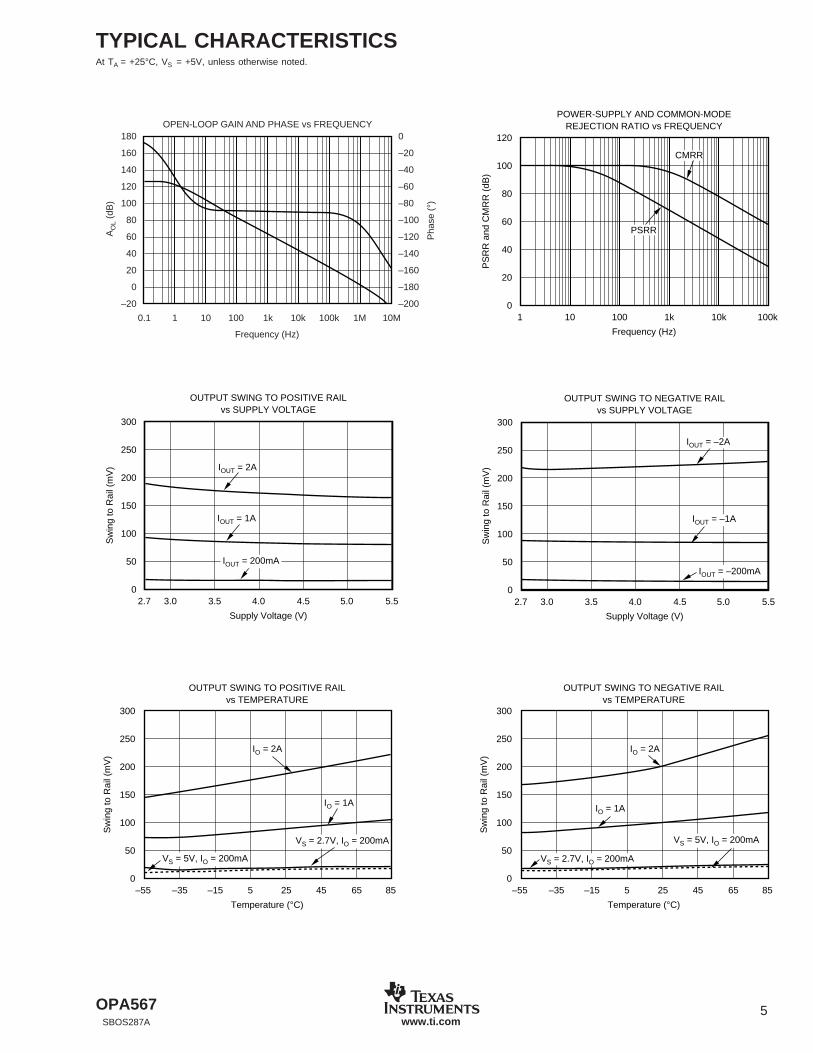
TYPICAL CHARACTERISTICSAt TA = +25°C, VS = +5V, unless otherwise noted.
180
160
140
120
100
80
60
40
20
0
–20
OPEN-LOOP GAIN AND PHASE vs FREQUENCY
Frequency (Hz)
1 10 100 1k 10k 100k 10M1M0.1
0
–20
–40
–60
–80
–100
–120
–140
–160
–180
–200
Pha
se (
°)
AO
L (d
B)
120
100
80
60
40
20
0
POWER-SUPPLY AND COMMON-MODEREJECTION RATIO vs FREQUENCY
Frequency (Hz)
PS
RR
and
CM
RR
(dB
)
1 10 100 1k 10k 100k
CMRR
PSRR
300
250
200
150
100
50
0
OUTPUT SWING TO POSITIVE RAILvs SUPPLY VOLTAGE
Supply Voltage (V)
Sw
ing
to R
ail (
mV
)
2.7 3.0 3.5 4.0 4.5 5.0 5.5
IOUT = 200mA
IOUT = 2A
IOUT = 1A
300
250
200
150
100
50
0
OUTPUT SWING TO NEGATIVE RAILvs SUPPLY VOLTAGE
Supply Voltage (V)
Sw
ing
to R
ail (
mV
)
2.7 3.0 3.5 4.0 4.5 5.0 5.5
IOUT = –200mA
IOUT = –2A
IOUT = –1A
300
250
200
150
100
50
0
OUTPUT SWING TO POSITIVE RAILvs TEMPERATURE
Temperature (°C)
Sw
ing
to R
ail (
mV
)
–55 –35 –15 5 25 45 65 85
IO = 2A
VS = 2.7V, IO = 200mA
IO = 1A
VS = 5V, IO = 200mA
300
250
200
150
100
50
0
OUTPUT SWING TO NEGATIVE RAILvs TEMPERATURE
Temperature (°C)
Sw
ing
to R
ail (
mV
)
–55 –35 –15 5 25 45 65 85
IO = 2A
VS = 5V, IO = 200mA
IO = 1A
VS = 2.7V, IO = 200mA
OPA567SBOS287A
6www.ti.com
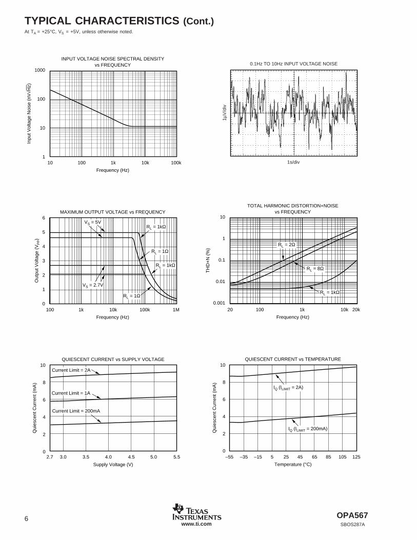
TYPICAL CHARACTERISTICS (Cont.)At TA = +25°C, VS = +5V, unless otherwise noted.
1000
100
10
1
INPUT VOLTAGE NOISE SPECTRAL DENSITYvs FREQUENCY
Frequency (Hz)
Inpu
t Vol
tage
Noi
se (
nV√H
z)
10 100 1k 10k 100k
0.1Hz TO 10Hz INPUT VOLTAGE NOISE
1µV
/div
1s/div
6
5
4
3
2
1
0
MAXIMUM OUTPUT VOLTAGE vs FREQUENCY
Frequency (Hz)
Out
put V
olta
ge (
VP
P)
100 1k 100k10k 1M
VS = 5VRL = 1kΩ
RL = 1Ω
RL = 1kΩ
VS = 2.7V
RL = 1Ω
10
1
0.1
0.01
0.001
TOTAL HARMONIC DISTORTION+NOISEvs FREQUENCY
Frequency (Hz)
TH
D+
N (
%)
20 100 1k 10k 20k
RL = 2Ω
RL = 8Ω
RL = 1kΩ
10
8
6
4
2
0
QUIESCENT CURRENT vs SUPPLY VOLTAGE
Supply Voltage (V)
Qui
esce
nt C
urre
nt (
mA
)
2.7 3.0 3.5 4.0 4.5 5.0 5.5
Current Limit = 1A
Current Limit = 2A
Current Limit = 200mA
10
8
6
4
2
0
QUIESCENT CURRENT vs TEMPERATURE
Temperature (°C)
Qui
esce
nt C
urre
nt (
mA
)
–55 –35 5–15 25 45 65 10585 125
IQ (ILIMIT = 2A)
IQ (ILIMIT = 200mA)
OPA567SBOS287A
7www.ti.com
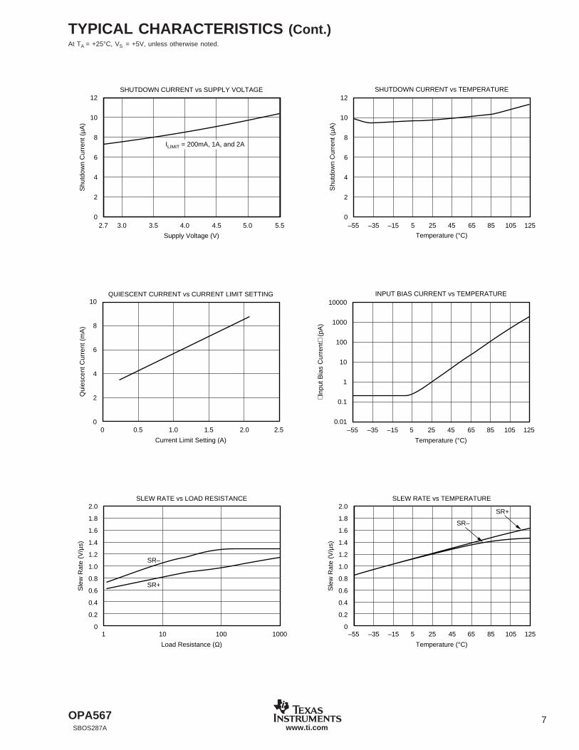
TYPICAL CHARACTERISTICS (Cont.)At TA = +25°C, VS = +5V, unless otherwise noted.
12
10
8
6
4
2
0
SHUTDOWN CURRENT vs SUPPLY VOLTAGE
Supply Voltage (V)
Shu
tdow
n C
urre
nt (
µA)
2.7 3.0 3.5 4.0 4.5 5.0 5.5
ILIMIT = 200mA, 1A, and 2A
SHUTDOWN CURRENT vs TEMPERATURE
Temperature (°C)
Shu
tdow
n C
urre
nt (
µA)
12
10
8
6
4
2
0–55 –35 5–15 25 45 65 10585 125
10
8
6
4
2
0
QUIESCENT CURRENT vs CURRENT LIMIT SETTING
Current Limit Setting (A)
Qui
esce
nt C
urre
nt (
mA
)
0 0.5 1.0 1.5 2.0 2.5
10000
1000
100
10
1
0.1
0.01
INPUT BIAS CURRENT vs TEMPERATURE
Temperature (°C)
Inp
ut B
ias
Cur
rent
(p
A)
–55 –35 –15 5 25 45 65 85 105 125
2.0
1.8
1.6
1.4
1.2
1.0
0.8
0.6
0.4
0.2
0
SLEW RATE vs LOAD RESISTANCE
Load Resistance (Ω)
Sle
w R
ate
(V/µ
s)
1 10
SR–
SR+
100 1000
2.0
1.8
1.6
1.4
1.2
1.0
0.8
0.6
0.4
0.2
0
SLEW RATE vs TEMPERATURE
Temperature (°C)
Sle
w R
ate
(V/µ
s)
–55 5 25 45–35 –15 65 85 105 125
SR–
SR+
OPA567SBOS287A
8www.ti.com
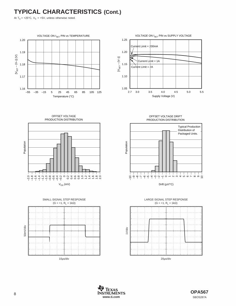
TYPICAL CHARACTERISTICS (Cont.)At TA = +25°C, VS = +5V, unless otherwise noted.
1.20
1.19
1.18
1.17
1.16
VOLTAGE ON ISET PIN vs TEMPERATURE
Temperature (°C)
[VS
ET –
(V
–)] (
V)
–55 –35 –15 5 65 85 10525 45 125
1.25
1.20
1.15
1.10
1.05
VOLTAGE ON ISET PIN vs SUPPLY VOLTAGE
Supply Voltage (V)
[VS
ET –
(V
–)]
2.7 3.0 3.5 4.0 4.5 5.0 5.5
Current Limit = 1A
Current Limit = 2A
Current Limit = 200mA
OFFSET VOLTAGEPRODUCTION DISTRIBUTION
VOS (mV)
–2.0
–1.8
–1.6
–1.4
–1.2
–1.0
Pop
ulat
ion
–0.8
–0.6
–0.4
–0.2 0
0.2
0.4
0.6
0.8
1.0
1.2
1.4
1.6
1.8
2.0
OFFSET VOLTAGE DRIFTPRODUCTION DISTRIBUTION
Pop
ulat
ion
Drift (µV/°C)
–10 –9 –8 –7 –6 –5 –4 –3 –2 –1 0 1 2 3 4 5 6 7 8 9 10
Typical ProductionDistribution ofPackaged Units.
SMALL-SIGNAL STEP RESPONSE(G = +1, RL = 1kΩ)
50m
V/d
iv
10µs/div
LARGE-SIGNAL STEP RESPONSE(G = +1, RL = 1kΩ)
1V/d
iv
20µs/div
OPA567SBOS287A
9www.ti.com
TYPICAL CHARACTERISTICS (Cont.)At TA = +25°C, VS = +5V, unless otherwise noted.
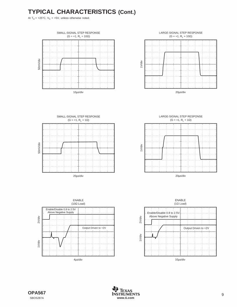
SMALL-SIGNAL STEP RESPONSE(G = +1, RL = 10Ω)
50m
V/d
iv
10µs/div
LARGE-SIGNAL STEP RESPONSE(G = +1, RL = 10Ω)
1V/d
iv
20µs/div
SMALL-SIGNAL STEP RESPONSE(G = +1, RL = 1Ω)
50m
V/d
iv
20µs/div
LARGE-SIGNAL STEP RESPONSE(G = +1, RL = 1Ω)
1V/d
iv
20µs/div
ENABLE(10Ω Load)
2V/d
iv1V
/div
4µs/div
Enable/Disable 0.8 to 2.5VAbove Negative Supply
Output Driven to +2V
ENABLE(1Ω Load)
10µs/div
Enable/Disable 0.8 to 2.5VAbove Negative Supply
Output Driven to +2V
1V/d
iv2V
/div
OPA567SBOS287A
10www.ti.com
TYPICAL CHARACTERISTICS (Cont.)At TA = +25°C, VS = +5V, unless otherwise noted.
DISABLE(10Ω Load)
200ns/div
Enable/Disable 0.8 to 2.5VAbove Negative Supply
Output Driven to +2V
2V/d
iv1V
/div
DISABLE(1Ω Load)
200ns/div
Enable/Disable 0.8 to 2.5VAbove Negative Supply
Output Drivento +2V
2V/d
iv1V
/div
POWER ON(1Ω Load)
1ms/div
Output Driven to +2V
Supply 0V to 5V5V/d
iv1V
/div
POWER OFF(1Ω Load)
1ms/div
1V/d
iv5V
/div
Output Driven to +2V
Supply 5V to 0V
IN AND OUT OF CURRENT LIMIT TRANSIENT(RL = 0.75Ω, Current Limit = 2A)
VO
UT
(2V
/div
)C
urre
nt L
imit
Fla
g(5
V/d
iv)
200µs/div
IN AND OUT OF CURRENT LIMIT TRANSIENT(RL = 7.5Ω, Current Limit = 200mA)
VO
UT
(2V
/div
)C
urre
nt L
imit
Fla
g(5
V/d
iv)
200µs/div

OPA567SBOS287A
11www.ti.com
TYPICAL CHARACTERISTICS (Cont.)At TA = +25°C, VS = +5V, unless otherwise noted.
OVERLOAD RECOVERY(G = +1)
1V/d
iv
40µs/div
VIN
VOUT
NO PHASE INVERSION WITH INPUTSLARGER THAN SUPPLY VOLTAGE
(G = +1, RL = 10Ω)
1V/d
iv
1ms/div
VIN
VOUT
15
10
5
0
–5
–10
–15
CURRENT LIMIT ERROR vs TEMPERATURE
Temperature (°C)
Cur
rent
Lim
it E
rror
(%
)
–55 –35
ILIMIT+ILIMIT –
–15 5 25 45 65 85
15
10
5
0
–5
–10
–15
CURRENT LIMIT ERROR vs OUTPUT CURRENT
Output Current (A)
Cur
rent
Lim
it E
rror
(%
)
0.2 0.4 0.6 0.8 1.0 1.2 1.4 1.6 1.8 2.0
ILIMIT+
ILIMIT –
50
40
30
20
10
0
OVERSHOOT vs LOAD CAPACITANCE(G = +1, RL = 1kΩ)
Load Capacitance (pF)
Ove
rsho
ot (
%)
10 100 1k 10k
15
10
5
0
–5
–10
–15
CURRENT LIMIT ERROR vs SUPPLY VOLTAGE
Supply Voltage (V)
Cur
rent
Lim
it E
rror
(%
)
ILIMIT+
ILIMIT –
2.7 3.0 3.5 4.0 4.5 5.0 5.5

OPA567SBOS287A
12www.ti.com
TYPICAL CHARACTERISTICS (Cont.)At TA = +25°C, VS = +5V, unless otherwise noted.
CLOSED-LOOP OUTPUT IMPEDANCEvs FREQUENCY
Frequency (Hz)
100k 1M 2M10k
Out
put I
mpe
danc
e (Ω
)
100
10
1
0.1
G = 1

OPA567SBOS287A
13www.ti.com
APPLICATIONS INFORMATIONBASIC CONFIGURATION
Figure 1 shows the OPA567 connected as a basic non-inverting amplifier. However, the OPA567 can be used invirtually any op amp configuration. A current limit settingresistor (RSET, in Figure 1) is essential to the OPA567operation, and cannot be omitted.
Power-supply terminals should be bypassed with low seriesimpedance capacitors. Using larger tantalum and smallerceramic type capacitors in parallel is recommended. Power-supply wiring should have low series impedance.
POWER SUPPLIES
The OPA567 operates with excellent performance from asingle (+2.7V to +5.5V) supply or from dual supplies. Powersupply voltages do not need to be equal as long as the totalvoltage remains below 5.5V. Parameters that vary signifi-cantly with operating voltage are shown in the TypicalCharacteristics section.
ADJUSTABLE CURRENT LIMIT AND CURRENTLIMIT FLAG PIN
The OPA567 provides over-current protection to the loadthrough its accurate, user-adjustable current limit (pin 6). Thecurrent limit value, ILIMIT, can be set from 0.2A to 2.2A bycontrolling the current to the ISET pin. The current limit, ILIMIT,will be 9800 • ISET, where ISET is the current through the ISET
pin. Setting the current limit requires no special powerresistors. The output current does not flow through this pin.
Setting the current limit
As illustrated in Figure 2, the simplest method of setting thecurrent limit is to connect a resistor or potentiometer between
FIGURE 1. Basic Connections.
FIGURE 2. Setting the Current Limit—Resistor Method.
the ISET pin and V–, the negative supply, according to theformula:
ILIMIT = 9800 • (1.18V/RSET)
Alternatively, the output current limit can be set by applyinga voltage source in series with a resistance using the equa-tion:
ILIMIT = 9800 • [(1.18V – VADJUST)/RSET]
The voltage source must be referenced to V–.
VIN
R1 R2
47µF
Enable(2)
47µF
0.1µF
ISET
47µF
1, 12
2, 3
8
9
11
64, 5
0.1µF RSET (Ω) ILIMIT
(A)
23.2k11.5k7.68k5.76k
0.51.01.52.0
RSET(1)
V+
NOTES: (1) RSET sets the current limit value from 0.2A to 2.2A. RSET can be a potentiometer to easily adjust current limit and calibrate out errors at the current limit node. (2) Enable—pull Low to disable output.
VO
V–
OPA567
RSET
VADJUST(1)
(b) Resistor/Voltage Source Method
NOTE: (1) This voltage source must be able tosink the current from the ISET pin, which is ILIMIT/9800.
1.18V
V–
ILIMIT = 9800 (1.18V – VADJUST)
RSET
ISET ISET
8
9
6
2, 3 2, 3
4, 5
8
9
6
4, 5
RPOT
(a) Resistor or Potentiometer Method
Putting a set resistor in series with the potentiometerwill prevent potential short-circuit on pin.
1.18V
V–
ILIMIT = 9800 (1.18V/RSET)

OPA567SBOS287A
14www.ti.com
Current Limit Accuracy
Internally separate circuits monitor the positive and negativecurrent limits. Each circuit output is compared to a singleinternal reference that is set by the user with an externalresistor or a resistor/voltage source combination. The OPA567employs a patented circuit technique to achieve an accurateand stable current limit throughout the full output range. Theinitial accuracy of the current limit is typically within 3%;however, because of internal matching limitations, the errorcan be as much as 15%. The variation of the current limit withfactors such as output current level, output voltage, andtemperature is shown in the Typical Characteristics section.
When the accuracy of one current limit (sourcing or sinking)is more important than the other, it is possible to set itsaccuracy to better than 1% by adjusting the external resistoror the applied voltage. The accuracy of the other current limitwill still be affected by internal matching.
Current Limit Flag Pin
The OPA567 features an IFLAG pin (pin 7) that can bemonitored to determine when the part is in current limit. Theoutput signal of the IFLAG pin is compatible to standard logicin single-supply applications. The output signal is a CMOSlogic gate that switches from V+ to V– to indicate that theamplifier is in current limit. The IFLAG pin can source and sinkup to 25µA. Additional parasitic capacitance between pins 6and 7 can cause instability at the edge of the current limit.Avoid routing these traces in parallel close to each other.
Quiescent Current Dependence on theCurrent Limit Setting
The OPA567 is a low-power amplifier, with a typical 3.4mAquiescent current (with the current limit configured for 200mA).The quiescent current varies with the current limit setting—it increases 0.5mA for each additional 200mA increase inthe current limit, as shown in Figure 3.
FIGURE 3. Quiescent Current vs Current Limit Setting.
ENABLE PIN—OUTPUT DISABLE
The Enable pin can disable the OPA567 within microsec-onds. When disabled, the amplifier draws less than 10µA andits output enters a high-impedance state that allows multi-plexing. It is important to note that when the amplifier isdisabled, the Thermal Flag pin (TFLAG) circuitry continues tooperate. This feature allows use of the TFLAG pin output toimplement thermal protection strategies. For more details,please see the section on thermal protection.
The OPA567 Enable pin has an internal pull-up circuit, so itdoes not have to be connected to the positive supply fornormal operation. To disable the amplifier, the Enable pinmust be connected to no more than (V–) + 0.8V. To enablethe amplifier, either allow the Enable pin to float or connectit to at least (V–) + 2.5V.
The Enable pin is referenced to the negative supply (V–).Therefore, shutdown operation is slightly different in single-supply and dual-supply applications.
In single-supply operation, V– typically equals commonground; thus, the enable/disable logic signal and the OPA567Enable pin are referenced to the same potential. In thisconfiguration, the logic level and the OPA567 Enable pin cansimply be tied together. Disabling the OPA567 occurs forvoltage levels of less than 0.8V. The OPA567 is enabled atlogic levels greater than 2.5V.
In dual-supply operation, the logic level is referenced to alogic ground. However, the OPA567 Enable pin is still refer-enced to V–. To disable the OPA567, the voltage level of thelogic signal needs to be level-shifted. This level-shifting canbe done using an optocoupler, as shown in Figure 4.
Examples of output behavior during disabled and enabledconditions with various load impedances are shown in thetypical characteristics section. Please note that this behavioris a function of board layout, load impedances, and bypassstrategies. For sensitive loads, the use of a low-pass filter orother protection strategy is recommended.
FIGURE 4. OPA567 Shutdown Configuration for DualSupplies.
10
8
6
4
2
0
QUIESCENT CURRENT vs CURRENT LIMIT SETTING
Current Limit Setting (A)
Qui
esce
nt C
urre
nt (
mA
)
0 0.5 1 1.5 2 2.5
Optocoupler
4N38
NOTE: (1) Optional—may be required to limit leakage current of optocouplerat high temperatures.
Enable
V+
VO
8
911
2, 3
4, 5
1, 12
(a) +5V (b) HCT or TTL In
HCT or TTL In
(a) (b)
OPA567
(1)
V–

OPA567SBOS287A
15www.ti.com
ENSURING MICROCONTROLLER COMPATIBILITY
Not all microcontrollers output the same logic state afterpower-up or reset. 8051-type microcontrollers, for example,output logic High levels on their ports while other modelspower up with logic Low levels after reset.
In configuration (a) shown in Figure 4, the enable/disablesignal is applied on the cathode side of the photodiode withinthe optocoupler. A logic High level causes the OPA567 to beenabled, and a logic Low level disables the OPA567. Inconfiguration (b) of Figure 4, with the logic signal applied onthe anode side, a high level disables the OPA567 and a lowlevel enables the op amp.
RAIL-TO-RAIL OUTPUT RANGE
The OPA567 has a class AB output stage with commonsource transistors that are used to achieve rail-to-rail outputswing. It was designed to be able to swing closer to the railthan other existing linear amplifiers, even with high outputcurrent levels. A quick way to estimate the output swing withvarious output current requirements is by using the equation:
VSWING [typical] = 0.1 • IO
Plots of the Output Swing vs Output Current, Supply Voltage,and Temperature are provided in the Typical Characteristicssection.
RAIL-TO-RAIL INPUT RANGE
The input common-mode voltage range of the OPA567extends 100mV beyond the supply rails. This is achieved bya complementary input stage with an N-channel input differ-ential pair in parallel with a P-channel differential pair. TheN-channel input pair is active for input voltages close to thepositive rail while the P-channel input pair is active for inputvoltages close to the negative rail. The transition point istypically at (V+) – 1.3V, and there is a small transition regionaround the switching point where both transistors are on. Itis important to note that the two input pairs can have offsetsof different signs and magnitudes. Therefore, as the transi-tion point is crossed, the offset of the amplifier changes. Thisoffset shift accounts for the reduced common-mode rejectionratio over the full input common-mode range.
OUTPUT PROTECTION
Reactive and EMF-generating loads can return load currentto the amplifier, causing the output voltage to exceed thepower-supply voltage. This damaging condition can beavoided with clamp diodes from the output terminal to thepower supplies, as shown in Figure 5. Schottky rectifierdiodes with a 3A or greater continuous rating are recom-mended.
THERMAL FLAG PIN
The OPA567 has thermal sensing circuitry that provides awarning signal when the die temperature exceeds safe limits.Unless the TFLAG pin is connected to the Enable pin, whenthis flag is triggered, the part continues to operate eventhough the junction temperature exceeds 150°C. This defaultoperation allows maximum usable operation in very harshconditions but degrades reliability. The TFLAG pin can be usedto provide for orderly system shutdown before failure occurs.It can be also used to evaluate the thermal environment todetermine need for and appropriate design of a shutdownmechanism.
The thermal flag output signal is from a CMOS logic gate thatswitches from V+ to V– to indicate that the amplifier is inthermal limit. This flag output pin can source and sink up to25µA. The TFLAG pin is HIGH during normal operation. Powerdissipated in the amplifier will cause the junction temperatureto rise. When the junction temperature exceeds 150°C, theTFLAG pin will go Low, and remain Low until the amplifier hascooled to 130°C. Despite this hysteresis, with a method oforderly shutdown, the TFLAG pin can cycle on and off, de-pending on load and signal conditions. This limits the dissi-pation of the amplifier but may have an undesirable effect onthe load.
It is possible to connect the TFLAG pin directly to the Enablepin for automatic shutdown protection. When both thermalshutdown and the amplifier enable/disable functions aredesired, the externally generated control signal and the TFLAG
pin outputs should be combined with an AND gate; seeFigure 6. The temperature protection was designed to pro-tect against overload conditions. It was not intended toreplace proper heatsinking. Continuously running the OPA567in and out of thermal shutdown will degrade reliability.
FIGURE 5. Output Protection Diode.
OPA567
Output Protection Diode
Output Protection Diode
ISET
RSET
VO
+V
1, 12
6
8
9
4, 5
–In
+In
2, 3
–V
OPA567SBOS287A
16www.ti.com
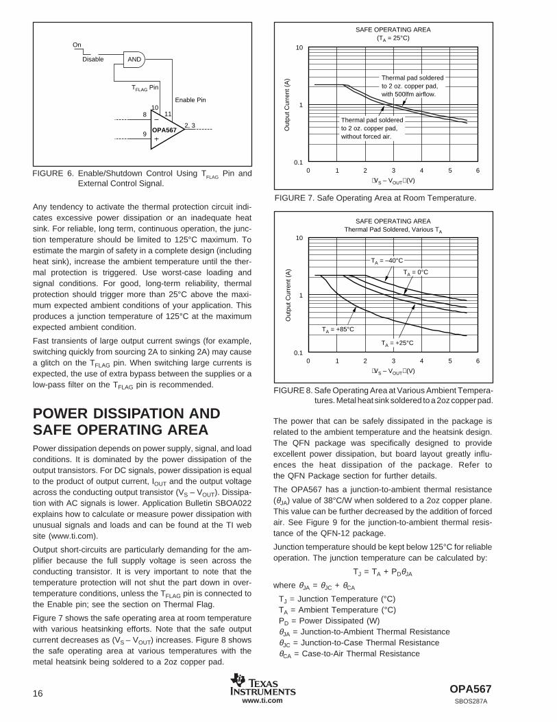
FIGURE 6. Enable/Shutdown Control Using TFLAG Pin andExternal Control Signal.
Any tendency to activate the thermal protection circuit indi-cates excessive power dissipation or an inadequate heatsink. For reliable, long term, continuous operation, the junc-tion temperature should be limited to 125°C maximum. Toestimate the margin of safety in a complete design (includingheat sink), increase the ambient temperature until the ther-mal protection is triggered. Use worst-case loading andsignal conditions. For good, long-term reliability, thermalprotection should trigger more than 25°C above the maxi-mum expected ambient conditions of your application. Thisproduces a junction temperature of 125°C at the maximumexpected ambient condition.
Fast transients of large output current swings (for example,switching quickly from sourcing 2A to sinking 2A) may causea glitch on the TFLAG pin. When switching large currents isexpected, the use of extra bypass between the supplies or alow-pass filter on the TFLAG pin is recommended.
POWER DISSIPATION ANDSAFE OPERATING AREAPower dissipation depends on power supply, signal, and loadconditions. It is dominated by the power dissipation of theoutput transistors. For DC signals, power dissipation is equalto the product of output current, IOUT and the output voltageacross the conducting output transistor (VS – VOUT). Dissipa-tion with AC signals is lower. Application Bulletin SBOA022explains how to calculate or measure power dissipation withunusual signals and loads and can be found at the TI website (www.ti.com).
Output short-circuits are particularly demanding for the am-plifier because the full supply voltage is seen across theconducting transistor. It is very important to note that thetemperature protection will not shut the part down in over-temperature conditions, unless the TFLAG pin is connected tothe Enable pin; see the section on Thermal Flag.
Figure 7 shows the safe operating area at room temperaturewith various heatsinking efforts. Note that the safe outputcurrent decreases as (VS – VOUT) increases. Figure 8 showsthe safe operating area at various temperatures with themetal heatsink being soldered to a 2oz copper pad.
FIGURE 7. Safe Operating Area at Room Temperature.
FIGURE 8. Safe Operating Area at Various Ambient Tempera-tures. Metal heat sink soldered to a 2oz copper pad.
The power that can be safely dissipated in the package isrelated to the ambient temperature and the heatsink design.The QFN package was specifically designed to provideexcellent power dissipation, but board layout greatly influ-ences the heat dissipation of the package. Refer tothe QFN Package section for further details.
The OPA567 has a junction-to-ambient thermal resistance(θJA) value of 38°C/W when soldered to a 2oz copper plane.This value can be further decreased by the addition of forcedair. See Figure 9 for the junction-to-ambient thermal resis-tance of the QFN-12 package.
Junction temperature should be kept below 125°C for reliableoperation. The junction temperature can be calculated by:
TJ = TA + PDθJA
where θJA = θJC + θCA
TJ = Junction Temperature (°C)TA = Ambient Temperature (°C)PD = Power Dissipated (W)θJA = Junction-to-Ambient Thermal ResistanceθJC = Junction-to-Case Thermal ResistanceθCA = Case-to-Air Thermal Resistance
Enable Pin
2, 3
118
9
TFLAG Pin
Disable
On
10
AND
OPA567
10
1
0.1
VS – VOUT (V)
SAFE OPERATING AREA(TA = 25°C)
Out
put C
urre
nt (
A)
0 1 2 3 4 5 6
Thermal pad solderedto 2 oz. copper pad,without forced air.
Thermal pad solderedto 2 oz. copper pad,with 500lfm airflow.
10
1
0.1
VS – VOUT (V)
SAFE OPERATING AREAThermal Pad Soldered, Various TA
Out
put C
urre
nt (
A)
0 1 2 3 4 5 6
TA = +85°C
TA = +25°C
TA = –40°C
TA = 0°C
OPA567SBOS287A
17www.ti.com
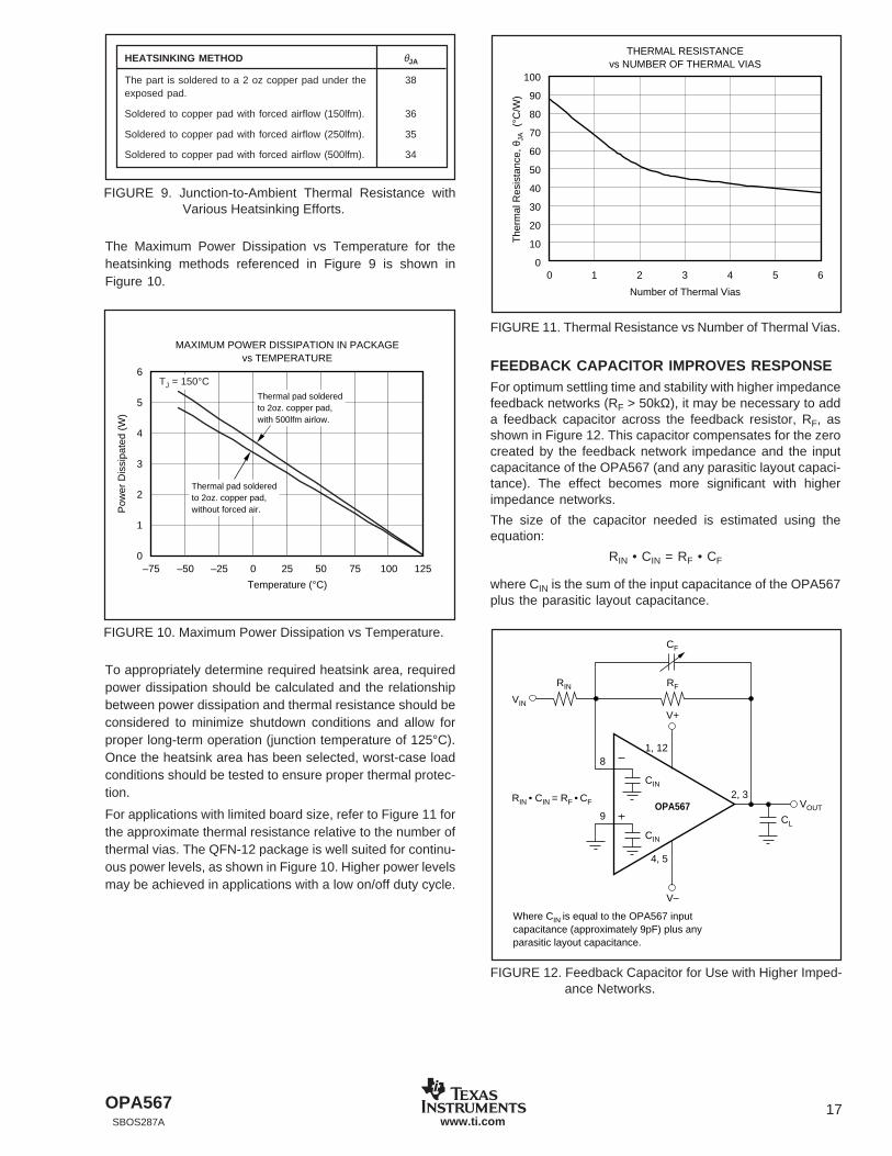
FIGURE 9. Junction-to-Ambient Thermal Resistance withVarious Heatsinking Efforts.
FIGURE 10. Maximum Power Dissipation vs Temperature.
FIGURE 11. Thermal Resistance vs Number of Thermal Vias.
FIGURE 12. Feedback Capacitor for Use with Higher Imped-ance Networks.
The Maximum Power Dissipation vs Temperature for theheatsinking methods referenced in Figure 9 is shown inFigure 10.
FEEDBACK CAPACITOR IMPROVES RESPONSEFor optimum settling time and stability with higher impedancefeedback networks (RF > 50kΩ), it may be necessary to adda feedback capacitor across the feedback resistor, RF, asshown in Figure 12. This capacitor compensates for the zerocreated by the feedback network impedance and the inputcapacitance of the OPA567 (and any parasitic layout capaci-tance). The effect becomes more significant with higherimpedance networks.
The size of the capacitor needed is estimated using theequation:
RIN • CIN = RF • CF
where CIN is the sum of the input capacitance of the OPA567plus the parasitic layout capacitance.
To appropriately determine required heatsink area, requiredpower dissipation should be calculated and the relationshipbetween power dissipation and thermal resistance should beconsidered to minimize shutdown conditions and allow forproper long-term operation (junction temperature of 125°C).Once the heatsink area has been selected, worst-case loadconditions should be tested to ensure proper thermal protec-tion.
For applications with limited board size, refer to Figure 11 forthe approximate thermal resistance relative to the number ofthermal vias. The QFN-12 package is well suited for continu-ous power levels, as shown in Figure 10. Higher power levelsmay be achieved in applications with a low on/off duty cycle.
OPA567
V+
V–
VOUT
VIN
RIN
81, 12
2, 3
4, 5
9
RIN • CIN = RF • CF
RF
CL
CIN
CIN
CF
Where CIN is equal to the OPA567 input capacitance (approximately 9pF) plus any parasitic layout capacitance.
HEATSINKING METHOD θJA
The part is soldered to a 2 oz copper pad under the 38exposed pad.
Soldered to copper pad with forced airflow (150lfm). 36
Soldered to copper pad with forced airflow (250lfm). 35
Soldered to copper pad with forced airflow (500lfm). 34
6
5
4
3
2
1
0
Temperature (°C)
MAXIMUM POWER DISSIPATION IN PACKAGEvs TEMPERATURE
Pow
er D
issi
pate
d (W
)
–75 –50 0–25 25 50 75 100 125
Thermal pad solderedto 2oz. copper pad,with 500lfm airlow.
Thermal pad solderedto 2oz. copper pad,without forced air.
TJ = 150°C
100
90
80
70
60
50
40
30
20
10
0
The
rmal
Res
ista
nce,
θJA
(°C
/W)
0 1 2 3 4 5 6
Number of Thermal Vias
THERMAL RESISTANCEvs NUMBER OF THERMAL VIAS

OPA567SBOS287A
18www.ti.com
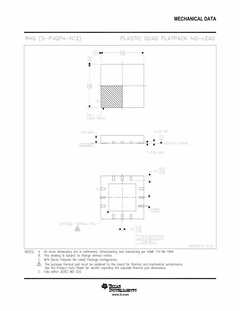
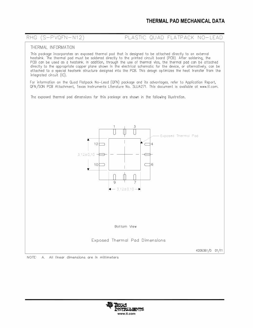
QFN THERMALLY ENHANCED PACKAGEThe OPA567 uses the QFN-12 package, a thermally-enhanced package designed to eliminate the use of bulkyheat sinks and slugs traditionally used in thermal packages.This package can be easily mounted using standard printedcircuit board (PCB) assembly techniques. See QFN/SONPCB Attachment Application Note (SLUA271) located atwww.ti.com.
The thermal resistance junction-to-ambient (RθJA) of the QFN
package depends on the PCB layout. Using thermal vias andwide PCB traces improve thermal resistance. The thermalpad must be soldered to the PCB. The thermal pad shouldeither be left floating or connected to V–.
LAYOUT GUIDELINESThe OPA567 is a power amplifier that requires proper layoutfor best performance. An example layout is appended to theend of this datasheet. Refinements to this layout may berequired based on assembly process requirements.
Keep power-supply leads as short as possible. This practicewill keep inductance low and resistive losses at a minimum.A minimum of 18 gauge wire thickness is recommended for
power- supply leads. The wire length should be less than 8inches.
Proper power-supply bypassing with low ESR capacitors isessential to achieve good performance. A parallel combina-tion of 100nF ceramic and 47µF tantalum bypass capacitorswill provide low impedance over a wide frequency range.Bypass capacitors should be placed as close as practical tothe power-supply pins of the OPA567.
PCB traces conducting high currents, such as from output toload or from the power-supply connector to the power-supplypins of the OPA567 should be kept as wide and short aspossible. This practice will keep inductance low and resistivelosses to a minimum.
The nine holes in the landing pattern for the OPA567 are forthe thermal vias that connect the thermal pad of the OPA567to the heatsink area on the PCB. All traces conducting highcurrents are very wide for lowest inductance and minimalresistive losses.
OPA567SBOS287A
19www.ti.com
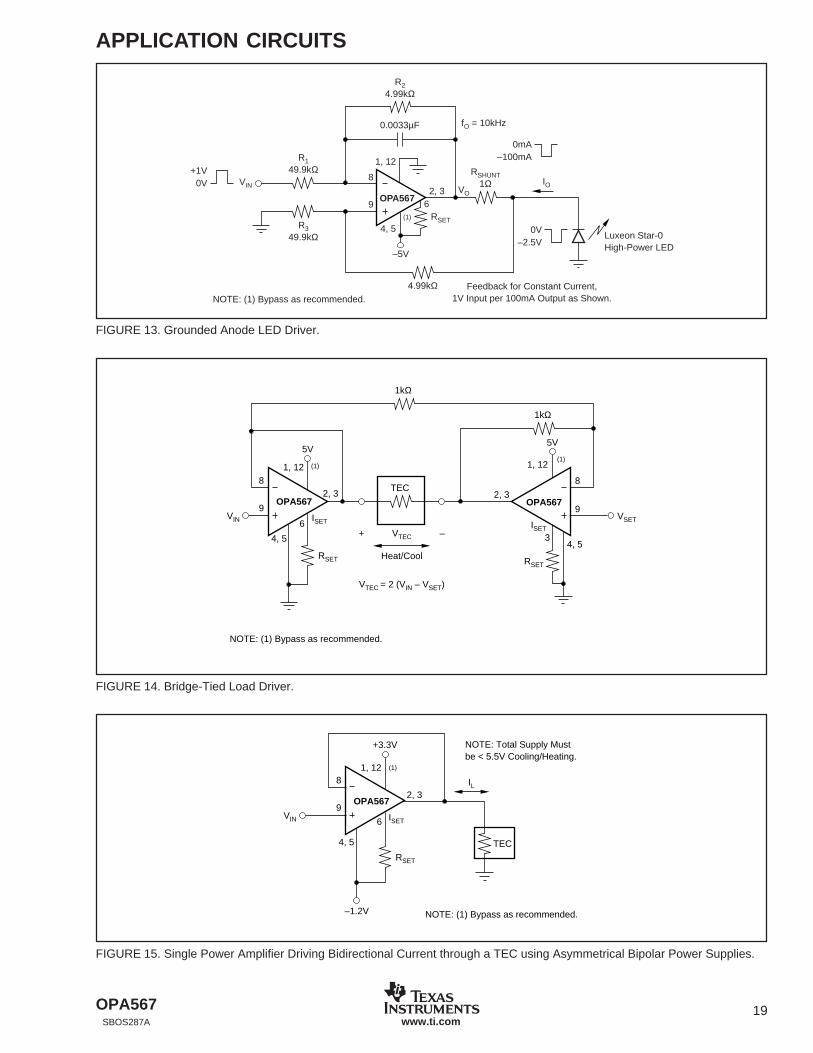
FIGURE 15. Single Power Amplifier Driving Bidirectional Current through a TEC using Asymmetrical Bipolar Power Supplies.
FIGURE 13. Grounded Anode LED Driver.
APPLICATION CIRCUITS
FIGURE 14. Bridge-Tied Load Driver.
Luxeon Star-0High-Power LED
1, 12
8
9
4, 5(1)
2, 36
RSET
VO
fO = 10kHz
VIN
OPA567
R149.9kΩ RSHUNT
1Ω IO
R24.99kΩ
4.99kΩ
0.0033µF
R349.9kΩ
–5V
+1V0V
0mA–100mA
0V–2.5V
Feedback for Constant Current,1V Input per 100mA Output as Shown.NOTE: (1) Bypass as recommended.
RSET
VSET
TEC
OPA567
1kΩ
Heat/Cool
VTEC
VTEC = 2 (VIN – VSET)
+ –
81, 12
4, 5
2, 3
ISET ISET
4, 5
8
9
3
6
1, 12
2, 3
RSET
NOTE: (1) Bypass as recommended.
5V
(1)
5V
9
1kΩ
VIN
OPA567
(1)
OPA567
81, 12
4, 5
6
–1.2V
2, 3
NOTE: Total Supply Mustbe < 5.5V Cooling/Heating.
NOTE: (1) Bypass as recommended.
RSET
ISET
+3.3V
(1)
9VIN
TEC
IL

PACKAGING INFORMATION
Orderable Device Status (1) PackageType
PackageDrawing
Pins PackageQty
Eco Plan (2) Lead/Ball Finish MSL Peak Temp (3)
OPA567AIRHGR ACTIVE VQFN RHG 12 2500 Green (RoHS &no Sb/Br)
CU NIPDAU Level-2-260C-1 YEAR
OPA567AIRHGRG4 ACTIVE VQFN RHG 12 2500 Green (RoHS &no Sb/Br)
CU NIPDAU Level-2-260C-1 YEAR
OPA567AIRHGT ACTIVE VQFN RHG 12 250 Green (RoHS &no Sb/Br)
CU NIPDAU Level-2-260C-1 YEAR
OPA567AIRHGTG4 ACTIVE VQFN RHG 12 250 Green (RoHS &no Sb/Br)
CU NIPDAU Level-2-260C-1 YEAR
(1) The marketing status values are defined as follows:ACTIVE: Product device recommended for new designs.LIFEBUY: TI has announced that the device will be discontinued, and a lifetime-buy period is in effect.NRND: Not recommended for new designs. Device is in production to support existing customers, but TI does not recommend using this part ina new design.PREVIEW: Device has been announced but is not in production. Samples may or may not be available.OBSOLETE: TI has discontinued the production of the device.
(2) Eco Plan - The planned eco-friendly classification: Pb-Free (RoHS), Pb-Free (RoHS Exempt), or Green (RoHS & no Sb/Br) - please checkhttp://www.ti.com/productcontent for the latest availability information and additional product content details.TBD: The Pb-Free/Green conversion plan has not been defined.Pb-Free (RoHS): TI's terms "Lead-Free" or "Pb-Free" mean semiconductor products that are compatible with the current RoHS requirementsfor all 6 substances, including the requirement that lead not exceed 0.1% by weight in homogeneous materials. Where designed to be solderedat high temperatures, TI Pb-Free products are suitable for use in specified lead-free processes.Pb-Free (RoHS Exempt): This component has a RoHS exemption for either 1) lead-based flip-chip solder bumps used between the die andpackage, or 2) lead-based die adhesive used between the die and leadframe. The component is otherwise considered Pb-Free (RoHScompatible) as defined above.Green (RoHS & no Sb/Br): TI defines "Green" to mean Pb-Free (RoHS compatible), and free of Bromine (Br) and Antimony (Sb) based flameretardants (Br or Sb do not exceed 0.1% by weight in homogeneous material)
(3) MSL, Peak Temp. -- The Moisture Sensitivity Level rating according to the JEDEC industry standard classifications, and peak soldertemperature.
Important Information and Disclaimer:The information provided on this page represents TI's knowledge and belief as of the date that it isprovided. TI bases its knowledge and belief on information provided by third parties, and makes no representation or warranty as to theaccuracy of such information. Efforts are underway to better integrate information from third parties. TI has taken and continues to takereasonable steps to provide representative and accurate information but may not have conducted destructive testing or chemical analysis onincoming materials and chemicals. TI and TI suppliers consider certain information to be proprietary, and thus CAS numbers and other limitedinformation may not be available for release.
In no event shall TI's liability arising out of such information exceed the total purchase price of the TI part(s) at issue in this document sold by TIto Customer on an annual basis.
PACKAGE OPTION ADDENDUM
www.ti.com 8-Dec-2009
Addendum-Page 1
TAPE AND REEL INFORMATION
*All dimensions are nominal
Device PackageType
PackageDrawing
Pins SPQ ReelDiameter
(mm)
ReelWidth
W1 (mm)
A0(mm)
B0(mm)
K0(mm)
P1(mm)
W(mm)
Pin1Quadrant
OPA567AIRHGR VQFN RHG 12 2500 330.0 12.4 5.3 5.3 1.5 8.0 12.0 Q2
OPA567AIRHGT VQFN RHG 12 250 180.0 12.4 5.3 5.3 1.5 8.0 12.0 Q2
PACKAGE MATERIALS INFORMATION
www.ti.com 14-Jul-2012
Pack Materials-Page 1

*All dimensions are nominal
Device Package Type Package Drawing Pins SPQ Length (mm) Width (mm) Height (mm)
OPA567AIRHGR VQFN RHG 12 2500 367.0 367.0 35.0
OPA567AIRHGT VQFN RHG 12 250 210.0 185.0 35.0
PACKAGE MATERIALS INFORMATION
www.ti.com 14-Jul-2012
Pack Materials-Page 2


IMPORTANT NOTICE
Texas Instruments Incorporated and its subsidiaries (TI) reserve the right to make corrections, enhancements, improvements and otherchanges to its semiconductor products and services per JESD46C and to discontinue any product or service per JESD48B. Buyers shouldobtain the latest relevant information before placing orders and should verify that such information is current and complete. Allsemiconductor products (also referred to herein as “components”) are sold subject to TI’s terms and conditions of sale supplied at the timeof order acknowledgment.
TI warrants performance of its components to the specifications applicable at the time of sale, in accordance with the warranty in TI’s termsand conditions of sale of semiconductor products. Testing and other quality control techniques are used to the extent TI deems necessaryto support this warranty. Except where mandated by applicable law, testing of all parameters of each component is not necessarilyperformed.
TI assumes no liability for applications assistance or the design of Buyers’ products. Buyers are responsible for their products andapplications using TI components. To minimize the risks associated with Buyers’ products and applications, Buyers should provideadequate design and operating safeguards.
TI does not warrant or represent that any license, either express or implied, is granted under any patent right, copyright, mask work right, orother intellectual property right relating to any combination, machine, or process in which TI components or services are used. Informationpublished by TI regarding third-party products or services does not constitute a license to use such products or services or a warranty orendorsement thereof. Use of such information may require a license from a third party under the patents or other intellectual property of thethird party, or a license from TI under the patents or other intellectual property of TI.
Reproduction of significant portions of TI information in TI data books or data sheets is permissible only if reproduction is without alterationand is accompanied by all associated warranties, conditions, limitations, and notices. TI is not responsible or liable for such altereddocumentation. Information of third parties may be subject to additional restrictions.
Resale of TI components or services with statements different from or beyond the parameters stated by TI for that component or servicevoids all express and any implied warranties for the associated TI component or service and is an unfair and deceptive business practice.TI is not responsible or liable for any such statements.
Buyer acknowledges and agrees that it is solely responsible for compliance with all legal, regulatory and safety-related requirementsconcerning its products, and any use of TI components in its applications, notwithstanding any applications-related information or supportthat may be provided by TI. Buyer represents and agrees that it has all the necessary expertise to create and implement safeguards whichanticipate dangerous consequences of failures, monitor failures and their consequences, lessen the likelihood of failures that might causeharm and take appropriate remedial actions. Buyer will fully indemnify TI and its representatives against any damages arising out of the useof any TI components in safety-critical applications.
In some cases, TI components may be promoted specifically to facilitate safety-related applications. With such components, TI’s goal is tohelp enable customers to design and create their own end-product solutions that meet applicable functional safety standards andrequirements. Nonetheless, such components are subject to these terms.
No TI components are authorized for use in FDA Class III (or similar life-critical medical equipment) unless authorized officers of the partieshave executed a special agreement specifically governing such use.
Only those TI components which TI has specifically designated as military grade or “enhanced plastic” are designed and intended for use inmilitary/aerospace applications or environments. Buyer acknowledges and agrees that any military or aerospace use of TI componentswhich have not been so designated is solely at the Buyer's risk, and that Buyer is solely responsible for compliance with all legal andregulatory requirements in connection with such use.
TI has specifically designated certain components which meet ISO/TS16949 requirements, mainly for automotive use. Components whichhave not been so designated are neither designed nor intended for automotive use; and TI will not be responsible for any failure of suchcomponents to meet such requirements.
Products Applications
Audio www.ti.com/audio Automotive and Transportation www.ti.com/automotive
Amplifiers amplifier.ti.com Communications and Telecom www.ti.com/communications
Data Converters dataconverter.ti.com Computers and Peripherals www.ti.com/computers
DLP® Products www.dlp.com Consumer Electronics www.ti.com/consumer-apps
DSP dsp.ti.com Energy and Lighting www.ti.com/energy
Clocks and Timers www.ti.com/clocks Industrial www.ti.com/industrial
Interface interface.ti.com Medical www.ti.com/medical
Logic logic.ti.com Security www.ti.com/security
Power Mgmt power.ti.com Space, Avionics and Defense www.ti.com/space-avionics-defense
Microcontrollers microcontroller.ti.com Video and Imaging www.ti.com/video
RFID www.ti-rfid.com
OMAP Mobile Processors www.ti.com/omap TI E2E Community e2e.ti.com
Wireless Connectivity www.ti.com/wirelessconnectivity
Mailing Address: Texas Instruments, Post Office Box 655303, Dallas, Texas 75265Copyright © 2012, Texas Instruments Incorporated