raising the efficiency ceiling in multijunction solar...
TRANSCRIPT
Raising the Efficiency Ceiling in Multijunction Solar Cells
Richard R. King
Spectrolab, Inc.A Boeing Company
Stanford Photonics Research Center SymposiumSep. 14-16, 2009
Stanford, CA
• Martha Symko-Davies, Fannie Posey-Eddy, Larry Kazmerski, Manuel Romero, Carl Osterwald, Keith Emery, John Geisz, Sarah Kurtz – NREL
• Angus Rockett – University of Illinois• Rosina Bierbaum – University of Michigan, Ann Arbor• Pierre Verlinden, John Lasich – Solar Systems, Australia• Kent Barbour, Andreea Boca, Dhananjay Bhusari, Ken Edmondson, Chris Fetzer,
William Hong, Jim Ermer, Russ Jones, Nasser Karam, Geoff Kinsey,Dimitri Krut, Diane Larrabee, Daniel Law, Phil Liu, Shoghig Mesropian, Mark Takahashi, and the entire multijunction solar cell team at Spectrolab
This work was supported in part by the U.S. Dept. of Energy through the NREL High-Performance Photovoltaics (HiPerf PV) program (ZAT-4-33624-12), the DOE Technology Pathways Partnership (TPP), and by Spectrolab.
AcknowledgmentsAcknowledgments
R. R. King, Stanford Photonics Research Center Symposium, Stanford, CA, Sep. 14-16, 2009 2
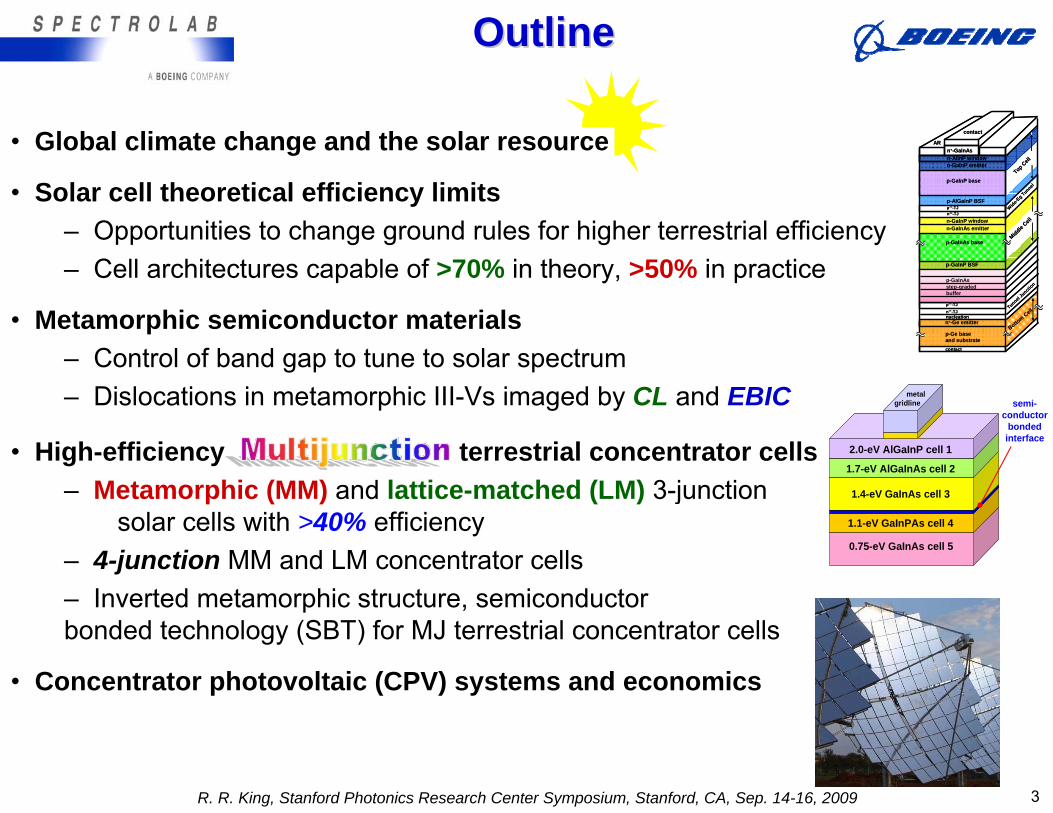
• Global climate change and the solar resource
• Solar cell theoretical efficiency limits– Opportunities to change ground rules for higher terrestrial efficiency– Cell architectures capable of >70% in theory, >50% in practice
• Metamorphic semiconductor materials– Control of band gap to tune to solar spectrum– Dislocations in metamorphic III-Vs imaged by CL and EBIC
OutlineOutline
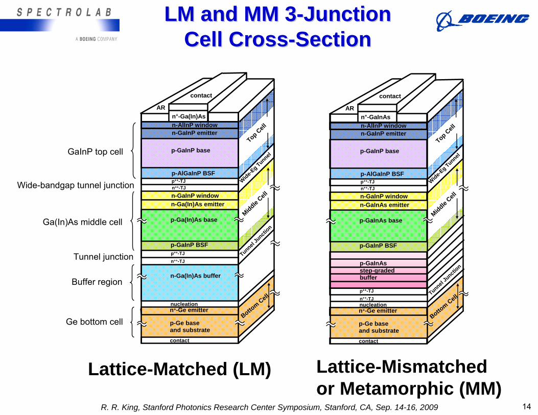
Tunnel Juncti
on
Top Cell
Wide-Eg Tunnel
Middle Cell
p-GaInP BSF
p-GaInP base
n-GaInAs emitter
n+-Ge emitter
p-AlGaInP BSF
n-GaInP emittern-AlInP windown+-GaInAs
contact
AR
p-Ge baseand substratecontact
p-GaInAsstep-graded buffer
Bottom Cell
p++-TJn++-TJ
p-GaInAs base
nucleation
n-GaInP window
p++-TJ
n++-TJTunnel J
unction
Top Cell
Wide-Eg Tunnel
Middle Cell
p-GaInP BSF
p-GaInP base
n-GaInAs emitter
n+-Ge emitter
p-AlGaInP BSF
n-GaInP emittern-AlInP windown+-GaInAs
contact
AR
p-Ge baseand substratecontact
p-GaInAsstep-graded buffer
Bottom Cell
p++-TJn++-TJ
p-GaInAs base
nucleation
n-GaInP window
p++-TJ
n++-TJ
• High-efficiency terrestrial concentrator cells– Metamorphic (MM) and lattice-matched (LM) 3-junction
solar cells with >40% efficiency– 4-junction MM and LM concentrator cells– Inverted metamorphic structure, semiconductor bonded technology (SBT) for MJ terrestrial concentrator cells
• Concentrator photovoltaic (CPV) systems and economics
0.75-eV GaInAs cell 5
1.1-eV GaInPAs cell 4
semi-conductor
bondedinterface
1.4-eV GaInAs cell 3
1.7-eV AlGaInAs cell 2
2.0-eV AlGaInP cell 1
metal gridline
R. R. King, Stanford Photonics Research Center Symposium, Stanford, CA, Sep. 14-16, 2009 3

Global Climate Change
R. R. King, Stanford Photonics Research Center Symposium, Stanford, CA, Sep. 14-16, 2009 4
Vostok Ice Core Data
Years Before Present
0
5000
0
1000
00
1500
00
2000
00
2500
00
3000
00
3500
00
4000
00
4500
00
Tem
pera
ture
(°C
)
-10
-8
-6
-4
-2
0
2
4
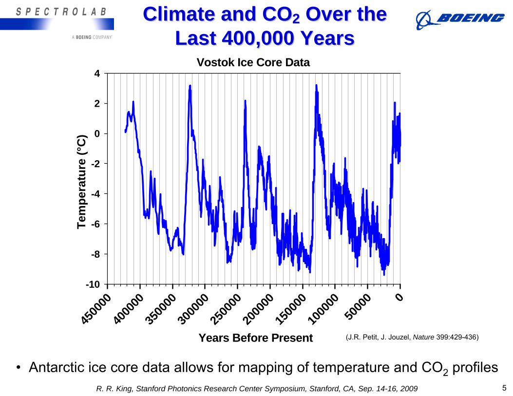
(J.R. Petit, J. Jouzel, Nature 399:429-436)
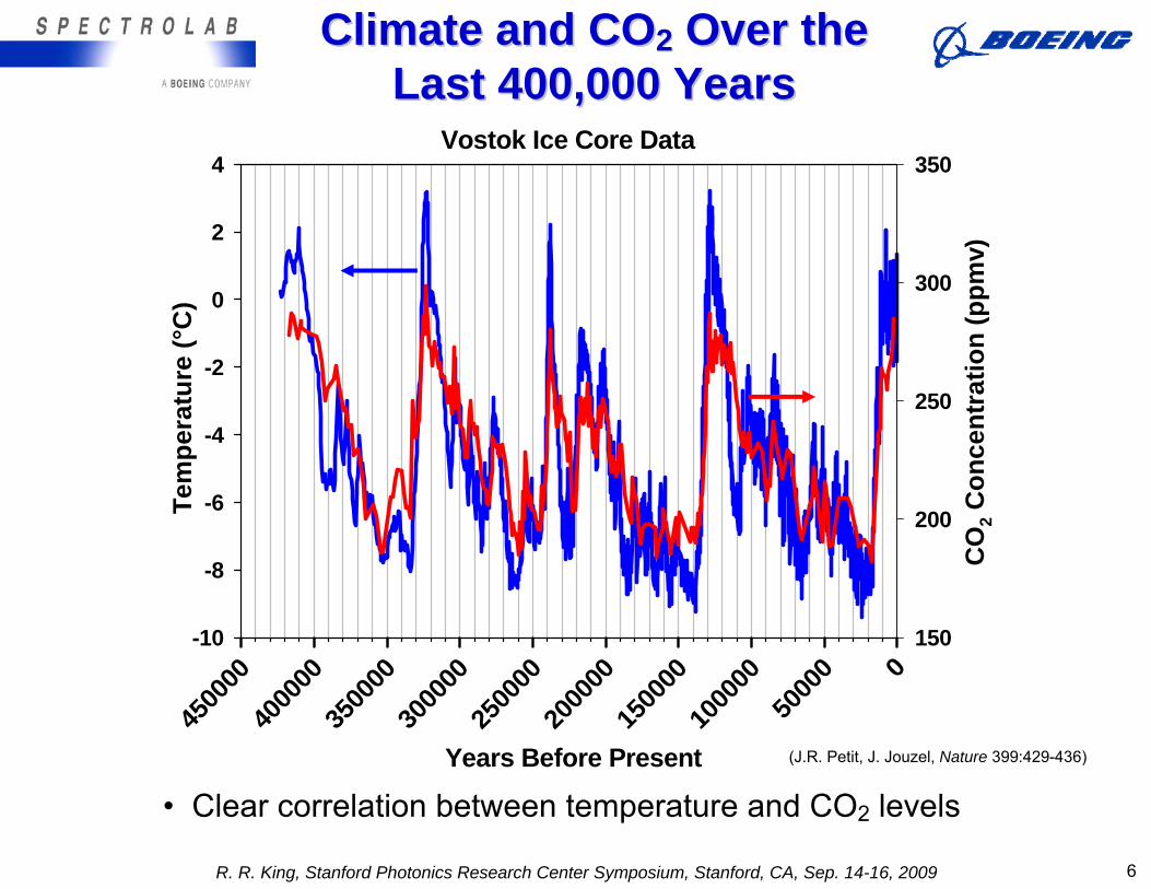
• Antarctic ice core data allows for mapping of temperature and CO2 profiles
Climate and COClimate and CO22 Over the Over the Last 400,000 YearsLast 400,000 Years
R. R. King, Stanford Photonics Research Center Symposium, Stanford, CA, Sep. 14-16, 2009 5
Climate and COClimate and CO22 Over the Over the Last 400,000 YearsLast 400,000 Years
Vostok Ice Core Data
Years Before Present
0
5000
0
1000
00
1500
00
2000
00
2500
00
3000
00
3500
00
4000
00
4500
00
Tem
pera
ture
(°C
)
-10
-8
-6
-4
-2
0
2
4
CO
2 Con
cent
ratio
n (p
pmv)
150
200
250
300
350
(J.R. Petit, J. Jouzel, Nature 399:429-436)
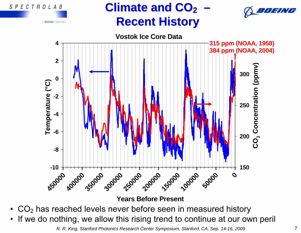
• Clear correlation between temperature and CO2 levels
R. R. King, Stanford Photonics Research Center Symposium, Stanford, CA, Sep. 14-16, 2009 6
Vostok Ice Core Data
Years Before Present
0
5000
0
1000
00
1500
00
2000
00
2500
00
3000
00
3500
00
4000
00
4500
00
Tem
pera
ture
(°C
)
-10
-8
-6
-4
-2
0
2
4
CO
2 Con
cent
ratio
n (p
pmv)
150
200
250
300
350315 ppm (NOAA, 1958)384 ppm (NOAA, 2004)
• CO2 has reached levels never before seen in measured history• If we do nothing, we allow this rising trend to continue at our own peril
Climate and COClimate and CO22 ––Recent HistoryRecent History
R. R. King, Stanford Photonics Research Center Symposium, Stanford, CA, Sep. 14-16, 2009 7
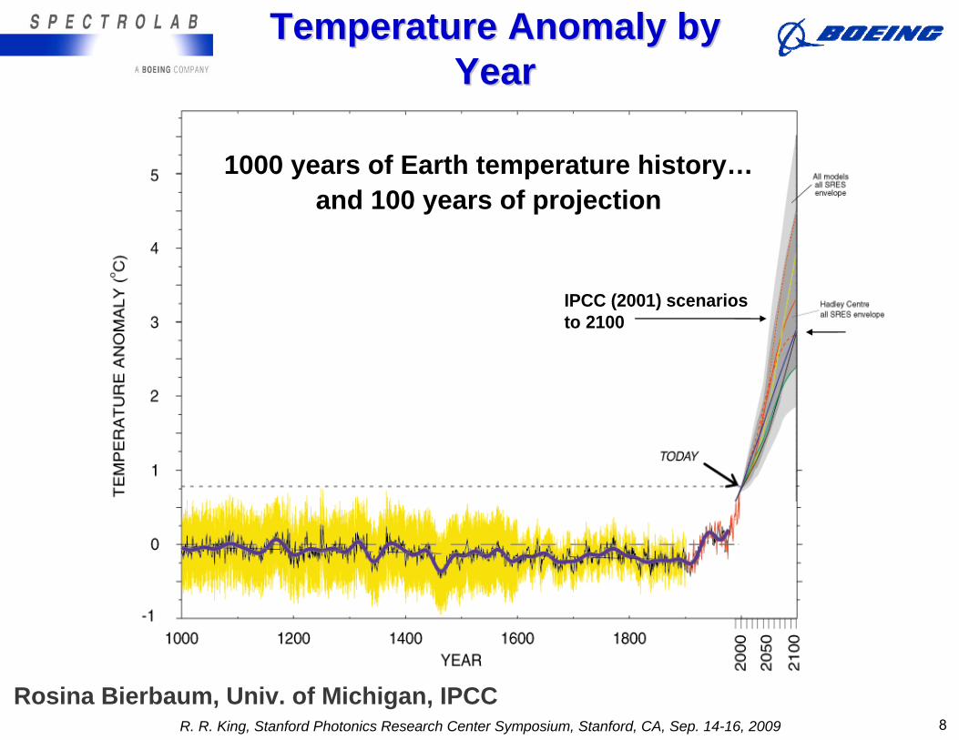
Rosina Bierbaum, Univ. of Michigan, IPCC
IPCC (2001) scenarios to 2100 IPCC (2001) scenarios to 2100
1000 years of Earth temperature history…and 100 years of projection
Temperature Anomaly by Temperature Anomaly by YearYear
R. R. King, Stanford Photonics Research Center Symposium, Stanford, CA, Sep. 14-16, 2009 8
The Solar Resource
R. R. King, Stanford Photonics Research Center Symposium, Stanford, CA, Sep. 14-16, 2009 9
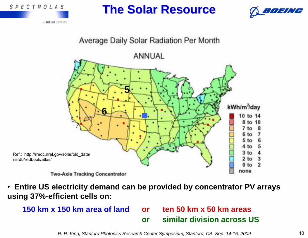
5
6
5
6
• Entire US electricity demand can be provided by concentrator PV arrays using 37%-efficient cells on:
or ten 50 km x 50 km areasor similar division across US
Ref.: http://rredc.nrel.gov/solar/old_data/nsrdb/redbook/atlas/
150 km x 150 km area of land
The Solar ResourceThe Solar Resource
R. R. King, Stanford Photonics Research Center Symposium, Stanford, CA, Sep. 14-16, 2009 10
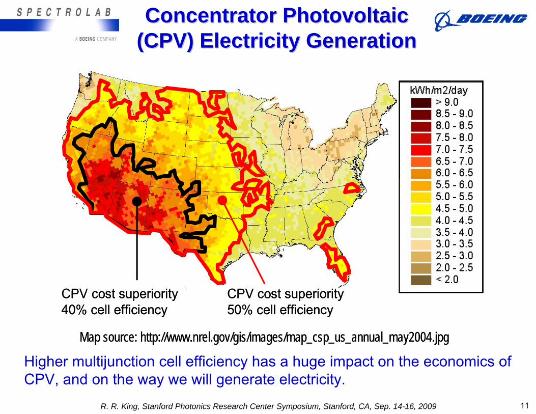
Map source: http://www.nrel.gov/gis/images/map_csp_us_annual_may2004.jpg
CPV cost superiority40% cell efficiency
CPV cost superiority50% cell efficiency
Map source: http://www.nrel.gov/gis/images/map_csp_us_annual_may2004.jpg
CPV cost superiority40% cell efficiency
CPV cost superiority50% cell efficiency
Concentrator Photovoltaic Concentrator Photovoltaic (CPV) Electricity Generation(CPV) Electricity Generation
Higher multijunction cell efficiency has a huge impact on the economics of CPV, and on the way we will generate electricity.
R. R. King, Stanford Photonics Research Center Symposium, Stanford, CA, Sep. 14-16, 2009 11
Solar Cell Theoretical
Efficiency
R. R. King, Stanford Photonics Research Center Symposium, Stanford, CA, Sep. 14-16, 2009 12
Ec
Ev
hν
0
100
200
300
400
500
600
700
0 0.5 1 1.5 2 2.5 3 3.5 4Photon Energy (eV)
Inte
nsity
per
Uni
t Pho
ton
Ener
gy
(W/m
2 .
eV)
0
0.2
0.4
0.6
0.8
1
1.2
1.4
Phot
on U
tiliz
atio
n Ef
ficie
ncy
AM1.5D, ASTM G173-03, 1000 W/m2
hν < Eg
0
100
200
300
400
500
600
700
0 0.5 1 1.5 2 2.5 3 3.5 4Photon Energy (eV)
Inte
nsity
per
Uni
t Pho
ton
Ener
gy
(W/m
2 .
eV)
0
0.2
0.4
0.6
0.8
1
1.2
1.4
Phot
on U
tiliz
atio
n Ef
ficie
ncy
AM1.5D, ASTM G173-03, 1000 W/m2Utilization efficiency of photon energy to bandgap Eg = 1.424 eV
hν > Eg
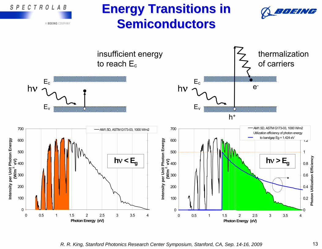
insufficient energy to reach Ec
thermalization of carriers
Ec
Ev
e-
h+
hν
Energy Transitions in Energy Transitions in SemiconductorsSemiconductors
R. R. King, Stanford Photonics Research Center Symposium, Stanford, CA, Sep. 14-16, 2009 13
Tunnel Ju
nction
Top Cell
Wide-Eg Tunnel
Middle Cell
p-GaInP BSF
p-GaInP base
n-Ga(In)As emitter
n+-Ge emitter
p-AlGaInP BSF
n-GaInP emittern-AlInP windown+-Ga(In)As
contact
AR
p-Ge baseand substratecontact
n-Ga(In)As buffer
Bottom Cell
p++-TJn++-TJ
p-Ga(In)As base
nucleation
Wide-bandgap tunnel junction
GaInP top cell
Ge bottom cell
n-GaInP window
p++-TJn++-TJ
Ga(In)As middle cell
Tunnel junction
Buffer regionTunnel
Juncti
on
Top Cell
Wide-Eg Tunnel
Middle Cell
p-GaInP BSF
p-GaInP base
n-GaInAs emitter
n+-Ge emitter
p-AlGaInP BSF
n-GaInP emittern-AlInP windown+-GaInAs
contact
AR
p-Ge baseand substratecontact
p-GaInAsstep-graded buffer
Bottom Cell
p++-TJn++-TJ
p-GaInAs base
nucleation
n-GaInP window
p++-TJn++-TJ
Lattice-Matched (LM) Lattice-Mismatchedor Metamorphic (MM)
LM and MM 3LM and MM 3--Junction Junction Cell CrossCell Cross--SectionSection
R. R. King, Stanford Photonics Research Center Symposium, Stanford, CA, Sep. 14-16, 2009 14
0
100
200
300
400
500
600
700
0 0.5 1 1.5 2 2.5 3 3.5 4Photon Energy (eV)
Inte
nsity
per
Uni
t Pho
ton
Ener
gy(W
/m 2
. eV
)
0
0.2
0.4
0.6
0.8
1
1.2
1.4
Phot
on u
tiliz
atio
n ef
ficie
ncy
.
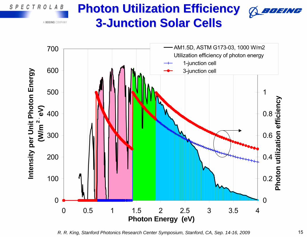
AM1.5D, ASTM G173-03, 1000 W/m2Utilization efficiency of photon energy 1-junction cell 3-junction cell
Photon Utilization EfficiencyPhoton Utilization Efficiency33--Junction Solar CellsJunction Solar Cells
R. R. King, Stanford Photonics Research Center Symposium, Stanford, CA, Sep. 14-16, 2009 15
Ec
Ev
hνEg
qφn
qVqφp
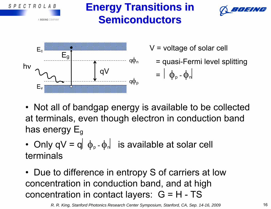
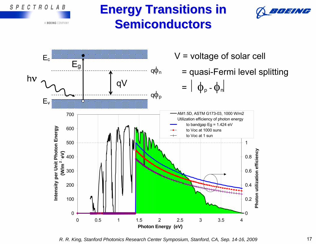
V = voltage of solar cell
= quasi-Fermi level splitting
= ⏐φp - φn⏐
• Not all of bandgap energy is available to be collected at terminals, even though electron in conduction band has energy Eg
• Only qV = q⏐φp - φn⏐ is available at solar cell terminals
• Due to difference in entropy S of carriers at low concentration in conduction band, and at high concentration in contact layers: G = H - TS
Energy Transitions in Energy Transitions in SemiconductorsSemiconductors
R. R. King, Stanford Photonics Research Center Symposium, Stanford, CA, Sep. 14-16, 2009 16
Ec
Ev
hνEg
qφn
qVqφp
V = voltage of solar cell
= quasi-Fermi level splitting
= ⏐φp - φn⏐
0
100
200
300
400
500
600
700
0 0.5 1 1.5 2 2.5 3 3.5 4Photon Energy (eV)
Inte
nsity
per
Uni
t Pho
ton
Ener
gy
(W/m
2 .
eV)
0
0.2
0.4
0.6
0.8
1
1.2
1.4
Phot
on u
tiliz
atio
n ef
ficie
ncy
AM1.5D, ASTM G173-03, 1000 W/m2Utilization efficiency of photon energy to bandgap Eg = 1.424 eV to Voc at 1000 suns to Voc at 1 sun
Energy Transitions in Energy Transitions in SemiconductorsSemiconductors
R. R. King, Stanford Photonics Research Center Symposium, Stanford, CA, Sep. 14-16, 2009 17
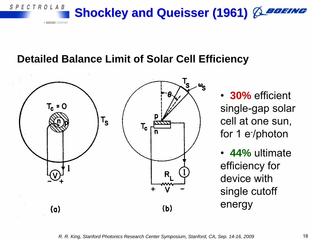
Detailed Balance Limit of Solar Cell Efficiency
• 30% efficient single-gap solar cell at one sun, for 1 e-/photon
• 44% ultimate efficiency for device with single cutoff energy
Shockley and Queisser (1961)Shockley and Queisser (1961)
R. R. King, Stanford Photonics Research Center Symposium, Stanford, CA, Sep. 14-16, 2009 18
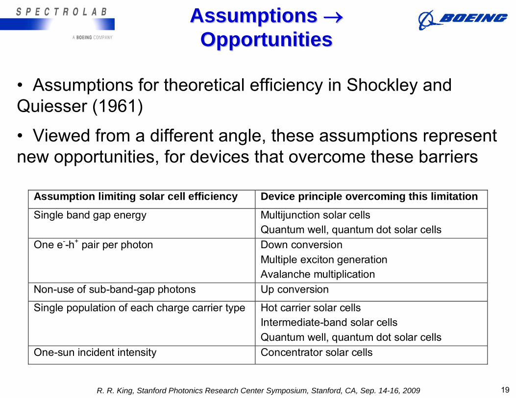
• Assumptions for theoretical efficiency in Shockley and Quiesser (1961)
• Viewed from a different angle, these assumptions represent new opportunities, for devices that overcome these barriers
Assumption limiting solar cell efficiency Device principle overcoming this limitation
Single band gap energy Multijunction solar cells Quantum well, quantum dot solar cells
One e--h+ pair per photon Down conversion Multiple exciton generation Avalanche multiplication
Non-use of sub-band-gap photons Up conversion
Single population of each charge carrier type Hot carrier solar cells Intermediate-band solar cells Quantum well, quantum dot solar cells
One-sun incident intensity Concentrator solar cells
Assumptions Assumptions →→OpportunitiesOpportunities
R. R. King, Stanford Photonics Research Center Symposium, Stanford, CA, Sep. 14-16, 2009 19
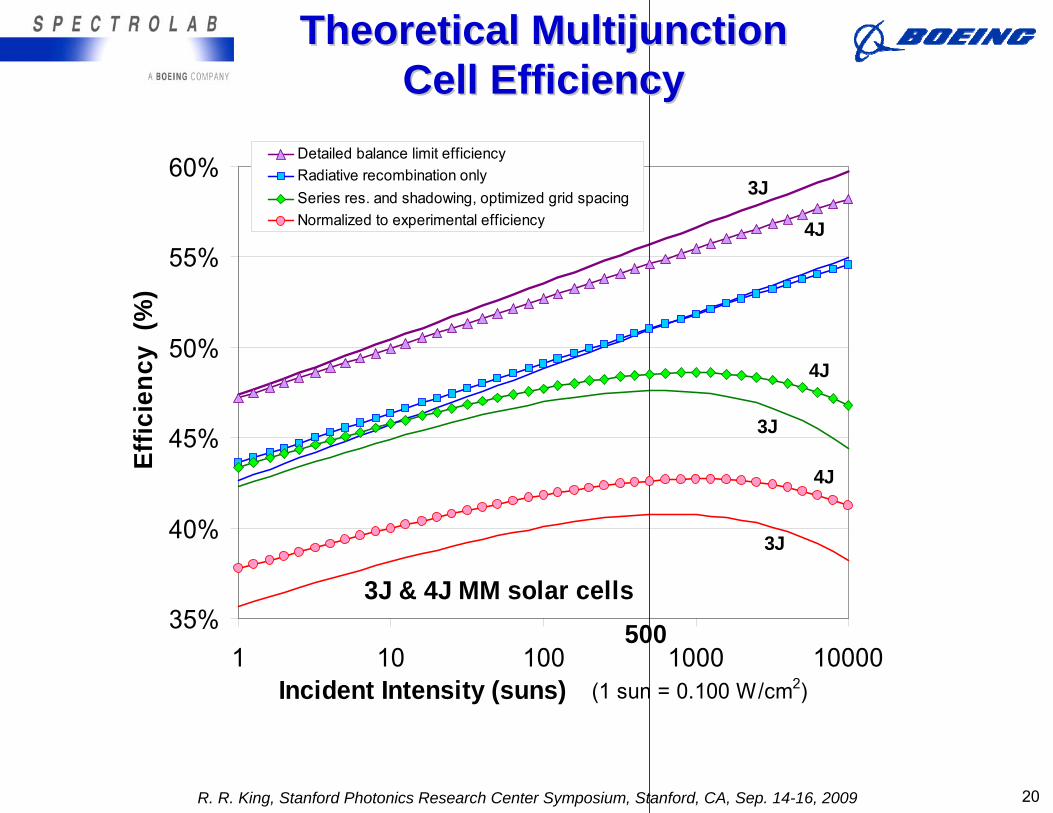
35%
40%
45%
50%
55%
60%
1 10 100 1000 10000Incident Intensity (suns) (1 sun = 0.100 W/cm2)
Effic
ienc
y (%
)Detailed balance limit efficiencyRadiative recombination onlySeries res. and shadowing, optimized grid spacingNormalized to experimental efficiency
5003J & 4J MM solar cells
3J
3J
3J
4J
4J
4J
Theoretical Multijunction Theoretical Multijunction Cell EfficiencyCell Efficiency
R. R. King, Stanford Photonics Research Center Symposium, Stanford, CA, Sep. 14-16, 2009 20
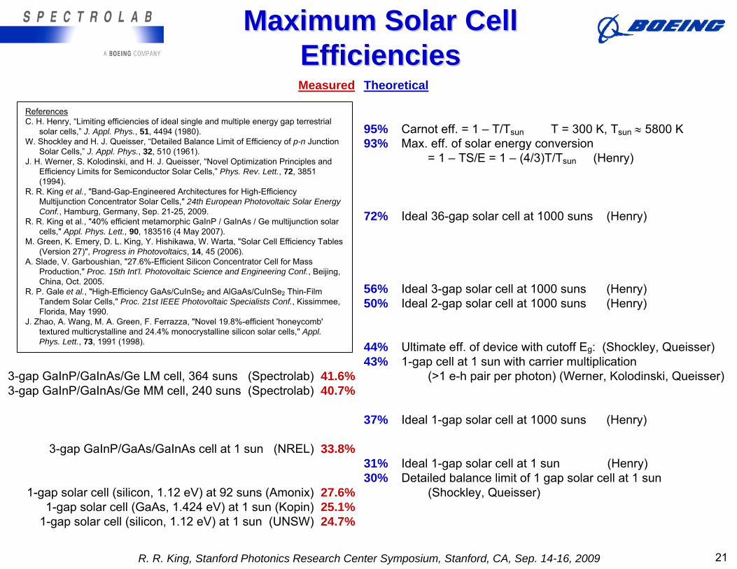
Theoretical
95% Carnot eff. = 1 – T/Tsun T = 300 K, Tsun ≈ 5800 K93% Max. eff. of solar energy conversion
= 1 – TS/E = 1 – (4/3)T/Tsun (Henry)
72% Ideal 36-gap solar cell at 1000 suns (Henry)
56% Ideal 3-gap solar cell at 1000 suns (Henry)50% Ideal 2-gap solar cell at 1000 suns (Henry)
44% Ultimate eff. of device with cutoff Eg: (Shockley, Queisser)43% 1-gap cell at 1 sun with carrier multiplication
(>1 e-h pair per photon) (Werner, Kolodinski, Queisser)
37% Ideal 1-gap solar cell at 1000 suns (Henry)
31% Ideal 1-gap solar cell at 1 sun (Henry)30% Detailed balance limit of 1 gap solar cell at 1 sun
(Shockley, Queisser)
Measured
3-gap GaInP/GaInAs/Ge LM cell, 364 suns (Spectrolab) 41.6%3-gap GaInP/GaInAs/Ge MM cell, 240 suns (Spectrolab) 40.7%
3-gap GaInP/GaAs/GaInAs cell at 1 sun (NREL) 33.8%
1-gap solar cell (silicon, 1.12 eV) at 92 suns (Amonix) 27.6%1-gap solar cell (GaAs, 1.424 eV) at 1 sun (Kopin) 25.1%
1-gap solar cell (silicon, 1.12 eV) at 1 sun (UNSW) 24.7%
ReferencesC. H. Henry, “Limiting efficiencies of ideal single and multiple energy gap terrestrial
solar cells,” J. Appl. Phys., 51, 4494 (1980). W. Shockley and H. J. Queisser, “Detailed Balance Limit of Efficiency of p-n Junction
Solar Cells,” J. Appl. Phys., 32, 510 (1961). J. H. Werner, S. Kolodinski, and H. J. Queisser, “Novel Optimization Principles and
Efficiency Limits for Semiconductor Solar Cells,” Phys. Rev. Lett., 72, 3851 (1994).
R. R. King et al., "Band-Gap-Engineered Architectures for High-Efficiency Multijunction Concentrator Solar Cells," 24th European Photovoltaic Solar Energy Conf., Hamburg, Germany, Sep. 21-25, 2009.
R. R. King et al., "40% efficient metamorphic GaInP / GaInAs / Ge multijunction solar cells," Appl. Phys. Lett., 90, 183516 (4 May 2007).
M. Green, K. Emery, D. L. King, Y. Hishikawa, W. Warta, "Solar Cell Efficiency Tables (Version 27)", Progress in Photovoltaics, 14, 45 (2006).
A. Slade, V. Garboushian, "27.6%-Efficient Silicon Concentrator Cell for Mass Production," Proc. 15th Int'l. Photovoltaic Science and Engineering Conf., Beijing, China, Oct. 2005.
R. P. Gale et al., "High-Efficiency GaAs/CuInSe2 and AlGaAs/CuInSe2 Thin-Film Tandem Solar Cells," Proc. 21st IEEE Photovoltaic Specialists Conf., Kissimmee, Florida, May 1990.
J. Zhao, A. Wang, M. A. Green, F. Ferrazza, "Novel 19.8%-efficient 'honeycomb' textured multicrystalline and 24.4% monocrystalline silicon solar cells," Appl. Phys. Lett., 73, 1991 (1998).
Maximum Solar Cell Maximum Solar Cell EfficienciesEfficiencies
R. R. King, Stanford Photonics Research Center Symposium, Stanford, CA, Sep. 14-16, 2009 21
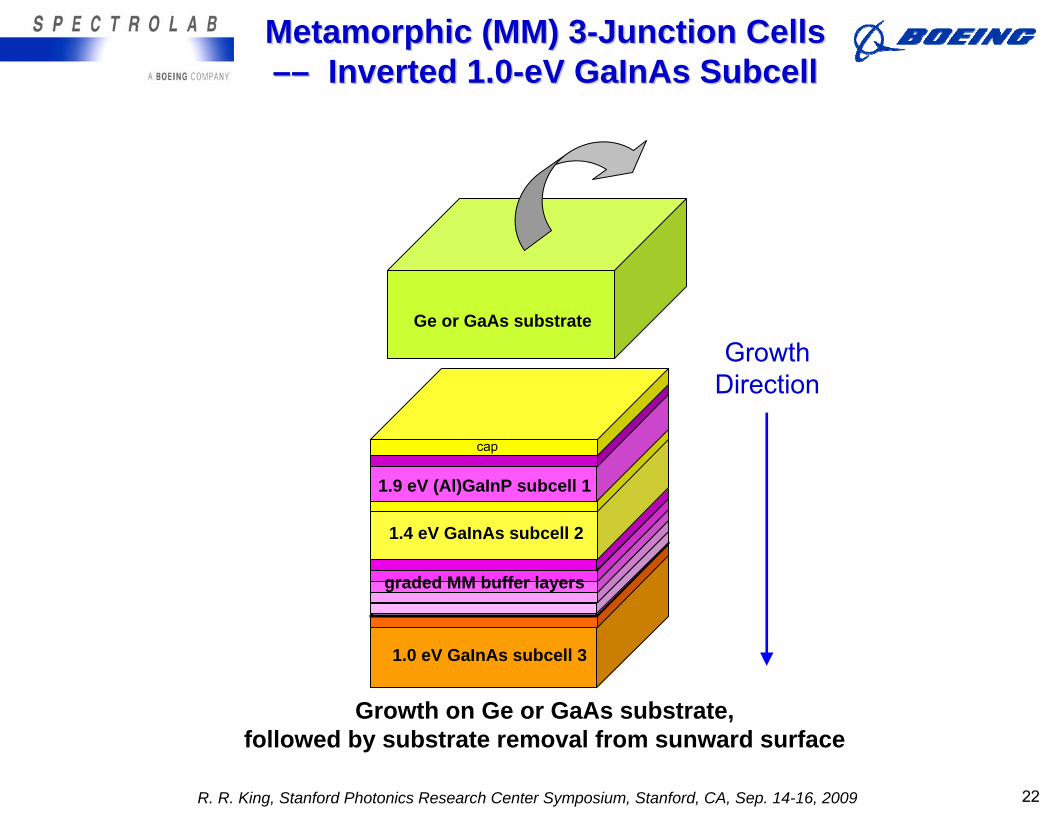
Growth on Ge or GaAs substrate, followed by substrate removal from sunward surface
GrowthDirection
cap
1.9 eV (Al)GaInP subcell 1
1.4 eV GaInAs subcell 2
graded MM buffer layers
1.0 eV GaInAs subcell 3
Ge or GaAs substrate
Ge or GaAs substrate
cap
Metamorphic (MM) 3Metamorphic (MM) 3--Junction Cells Junction Cells –––– Inverted 1.0Inverted 1.0--eV GaInAs SubcelleV GaInAs Subcell
R. R. King, Stanford Photonics Research Center Symposium, Stanford, CA, Sep. 14-16, 2009 22
0
10
20
30
40
50
60
70
80
90
100
300 500 700 900 1100 1300 1500 1700 1900Wavelength (nm)
Cur
rent
Den
sity
per
Uni
t W
avel
engt
h (m
A/(c
m2 μ
m))
0
10
20
30
40
50
60
70
80
90
100
Exte
rnal
Qua
ntum
Effi
cien
cy (
%)
AM1.5D, low-AOD
AM1.5G, ASTM G173-03
AM0, ASTM E490-00a
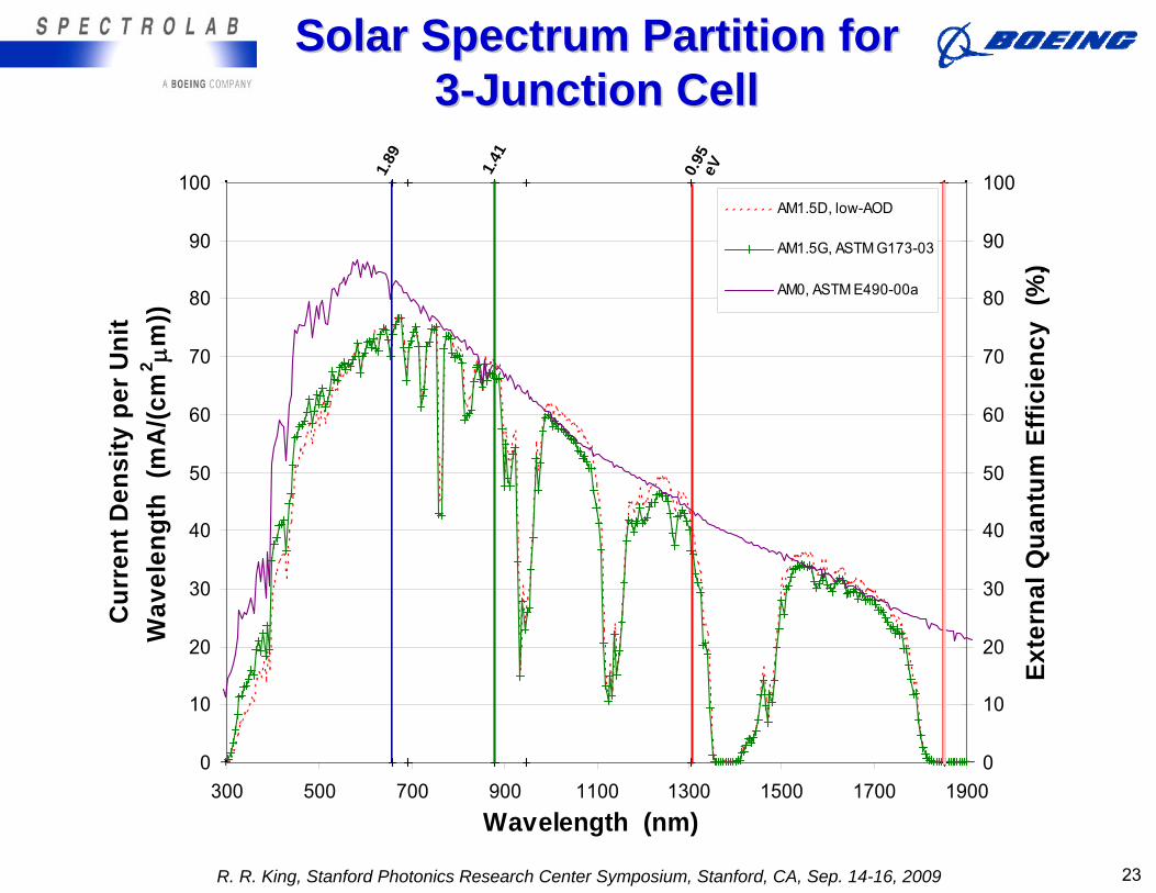
1.89 1.41 eV0.67
0.95
eV
Solar Spectrum Partition for Solar Spectrum Partition for 33--Junction CellJunction Cell
R. R. King, Stanford Photonics Research Center Symposium, Stanford, CA, Sep. 14-16, 2009 23
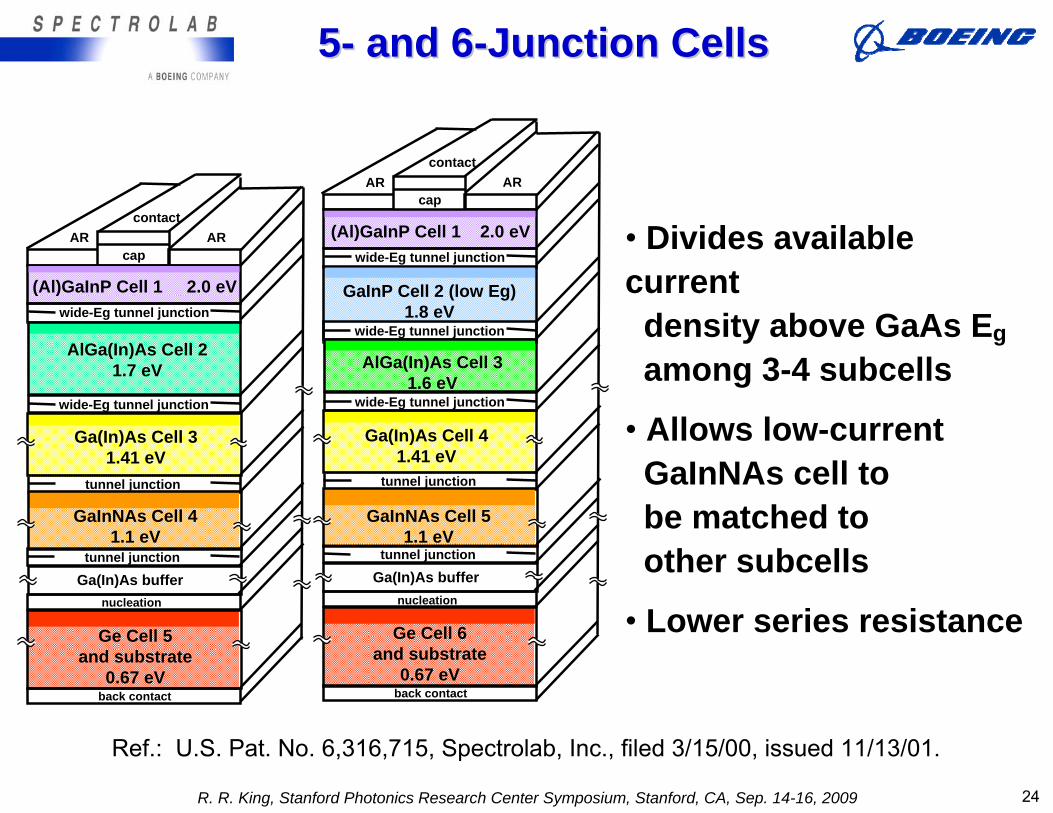
cap
contactAR
(Al)GaInP Cell 1 2.0 eVwide-Eg tunnel junction
AlGa(In)As Cell 21.7 eV
tunnel junction
Ga(In)As Cell 31.41 eV
tunnel junction
AR
Ga(In)As buffer
Ge Cell 5and substrate
0.67 eV
nucleation
back contact
wide-Eg tunnel junction
GaInNAs Cell 41.1 eV
cap
contactAR
(Al)GaInP Cell 1 2.0 eVwide-Eg tunnel junction
GaInP Cell 2 (low Eg)1.8 eV
wide-Eg tunnel junction
AlGa(In)As Cell 31.6 eV
tunnel junction
Ga(In)As Cell 41.41 eV
tunnel junction
AR
Ga(In)As buffer
Ge Cell 6and substrate
0.67 eV
nucleation
back contact
wide-Eg tunnel junction
GaInNAs Cell 51.1 eV
• Divides available current
density above GaAs Eg
among 3-4 subcells
• Allows low-currentGaInNAs cell to be matched toother subcells
• Lower series resistance
Ref.: U.S. Pat. No. 6,316,715, Spectrolab, Inc., filed 3/15/00, issued 11/13/01.
55-- and 6and 6--Junction CellsJunction Cells
R. R. King, Stanford Photonics Research Center Symposium, Stanford, CA, Sep. 14-16, 2009 24
0
100
200
300
400
500
600
700
0 0.5 1 1.5 2 2.5 3 3.5 4Photon Energy (eV)
Inte
nsity
per
Uni
t Pho
ton
Ener
gy(W
/m 2
. eV
)
0
0.2
0.4
0.6
0.8
1
1.2
1.4
Phot
on u
tiliz
atio
n ef
ficie
ncy
.
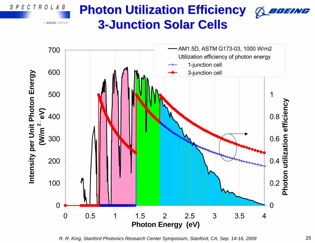
AM1.5D, ASTM G173-03, 1000 W/m2Utilization efficiency of photon energy 1-junction cell 3-junction cell
Photon Utilization EfficiencyPhoton Utilization Efficiency33--Junction Solar CellsJunction Solar Cells
R. R. King, Stanford Photonics Research Center Symposium, Stanford, CA, Sep. 14-16, 2009 25

0
100
200
300
400
500
600
700
0 0.5 1 1.5 2 2.5 3 3.5 4Photon Energy (eV)
Inte
nsity
per
Uni
t Pho
ton
Ener
gy(W
/m 2
. eV
)
0
0.2
0.4
0.6
0.8
1
1.2
1.4
Phot
on u
tiliz
atio
n ef
ficie
ncy
.
AM1.5D, ASTM G173-03, 1000 W/m2Utilization efficiency of photon energy 1-junction cell 3-junction cell 6-junction cell
Photon Utilization EfficiencyPhoton Utilization Efficiency66--Junction Solar CellsJunction Solar Cells
R. R. King, Stanford Photonics Research Center Symposium, Stanford, CA, Sep. 14-16, 2009 26
0
10
20
30
40
50
60
70
80
90
100R
emai
ning
Fra
ctio
n of
Ava
ilabl
e Po
wer
(%)
0
10
20
30
40
50
60
70
80
90
100
photonenergiesin solar
spectrum
after carrierthermalizationto band edges
photonswith energy
above lowestband gap
6-junctionterrestrial
concentratorcell
morebalanced
1.9/1.4/1.0 eVbandgap
combination
after carrierextractionat quasi-
Fermi levels-- 1-sun
after carrierextractionat quasi-
Fermi levels-- 500 suns
subcell 1 (top)
39%
subcell 3
31%
subcell 2
26%
no photogeneration
31%
20%
23%
11%
17%
25%
8%
17%
25%
5%
15%
23%
4%7%
8%
10%
14%
12%0
10
20
30
40
50
60
70
80
90
100
Rem
aini
ng F
ract
ion
of A
vaila
ble
Pow
er (%
)
0
10
20
30
40
50
60
70
80
90
100
photonenergiesin solar
spectrum
after carrierthermalizationto band edges
photonswith energy
above lowestband gap
6-junctionterrestrial
concentratorcell
morebalanced
1.9/1.4/1.0 eVbandgap
combination
after carrierextractionat quasi-
Fermi levels-- 1-sun
after carrierextractionat quasi-
Fermi levels-- 500 suns
subcell 1 (top)
39%
subcell 3
31%
subcell 2
26%
no photogeneration
31%
20%
23%
11%
17%
25%
8%
17%
25%
5%
15%
23%
4%7%
8%
10%
14%
12%
Ec
Ev
hνEc
Ev
hν
0
100
200
300
400
500
600
700
0 0.5 1 1.5 2 2.5 3 3.5 4Photon Energy (eV)
Inte
nsity
per
Uni
t Pho
ton
Ener
gy
(W/m
2 . eV
)
0
0.2
0.4
0.6
0.8
1
1.2
1.4
Phot
on U
tiliz
atio
n Ef
ficie
ncy
AM1.5D, ASTM G173-03, 1000 W/m2
hν < Eg
0
100
200
300
400
500
600
700
0 0.5 1 1.5 2 2.5 3 3.5 4Photon Energy (eV)
Inte
nsity
per
Uni
t Pho
ton
Ener
gy
(W/m
2 . eV
)
0
0.2
0.4
0.6
0.8
1
1.2
1.4
Phot
on U
tiliz
atio
n Ef
ficie
ncy
AM1.5D, ASTM G173-03, 1000 W/m2Utilization efficiency of photon energy to bandgap Eg = 1.424 eV
hν > Eg
thermalization of carriers
Ec
Ev
e-
h+
hνEc
Ev
e-
h+
hν Ec
Ev
hνEg
qφn
qVqφp
Ec
Ev
hνEg
qφn
qVqφp
0
100
200
300
400
500
600
700
0 0.5 1 1.5 2 2.5 3 3.5 4Photon Energy (eV)
Inte
nsity
per
Uni
t Pho
ton
Ener
gy
(W/m
2 .
eV)
0
0.2
0.4
0.6
0.8
1
1.2
1.4
Phot
on u
tiliz
atio
n ef
ficie
ncy
AM1.5D, ASTM G173-03, 1000 W/m2Utilization efficiency of photon energy to bandgap Eg = 1.424 eV to Voc at 1000 suns to Voc at 1 sun
GrowthDirection
cap
1.9 eV (Al)GaInP subcell 1
1.4 eV GaInAs subcell 2
graded MM buffer layers
1.0 eV GaInAs subcell 3
GrowthDirection
cap
1.9 eV (Al)GaInP subcell 1
1.4 eV GaInAs subcell 2
graded MM buffer layers
1.0 eV GaInAs subcell 3
cap
1.9 eV (Al)GaInP subcell 1
1.4 eV GaInAs subcell 2
graded MM buffer layers
1.0 eV GaInAs subcell 3
Ge or GaAs substrateGe or GaAs substrate
Ge or GaAs substrate
cap
Ge or GaAs substrateGe or GaAs substrate
capcap
0
100
200
300
400
500
600
700
0 0.5 1 1.5 2 2.5 3 3.5 4Photon Energy (eV)
Inte
nsity
per
Uni
t Pho
ton
Ener
gy(W
/m 2
. eV
)
0
0.2
0.4
0.6
0.8
1
1.2
1.4
Phot
on u
tiliz
atio
n ef
ficie
ncy
.
AM1.5D, ASTM G173-03, 1000 W/m2Utilization efficiency of photon energy 1-junction cell 3-junction cell 6-junction cell
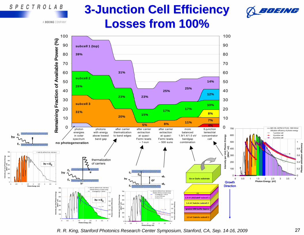
33--Junction Cell Efficiency Junction Cell Efficiency Losses from 100% Losses from 100%
R. R. King, Stanford Photonics Research Center Symposium, Stanford, CA, Sep. 14-16, 2009 27
Metamorphic
Semiconductor
Materials
R. R. King, Stanford Photonics Research Center Symposium, Stanford, CA, Sep. 14-16, 2009 28
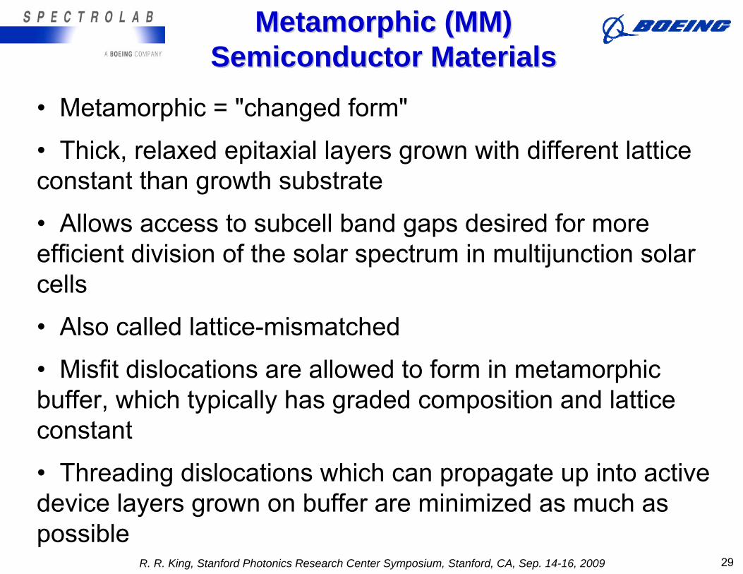
• Metamorphic = "changed form"
• Thick, relaxed epitaxial layers grown with different lattice constant than growth substrate
• Allows access to subcell band gaps desired for more efficient division of the solar spectrum in multijunction solar cells
• Also called lattice-mismatched
• Misfit dislocations are allowed to form in metamorphic buffer, which typically has graded composition and lattice constant
• Threading dislocations which can propagate up into active device layers grown on buffer are minimized as much as possible
Metamorphic (MM) Metamorphic (MM) Semiconductor MaterialsSemiconductor Materials
R. R. King, Stanford Photonics Research Center Symposium, Stanford, CA, Sep. 14-16, 2009 29
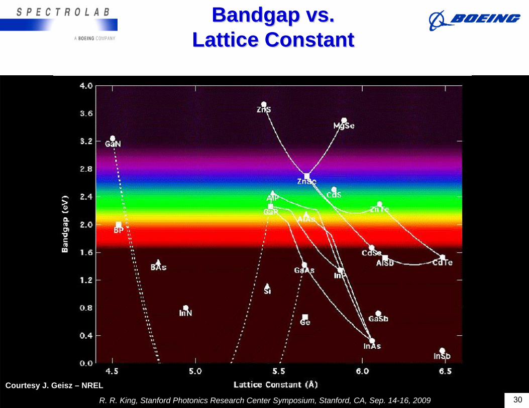
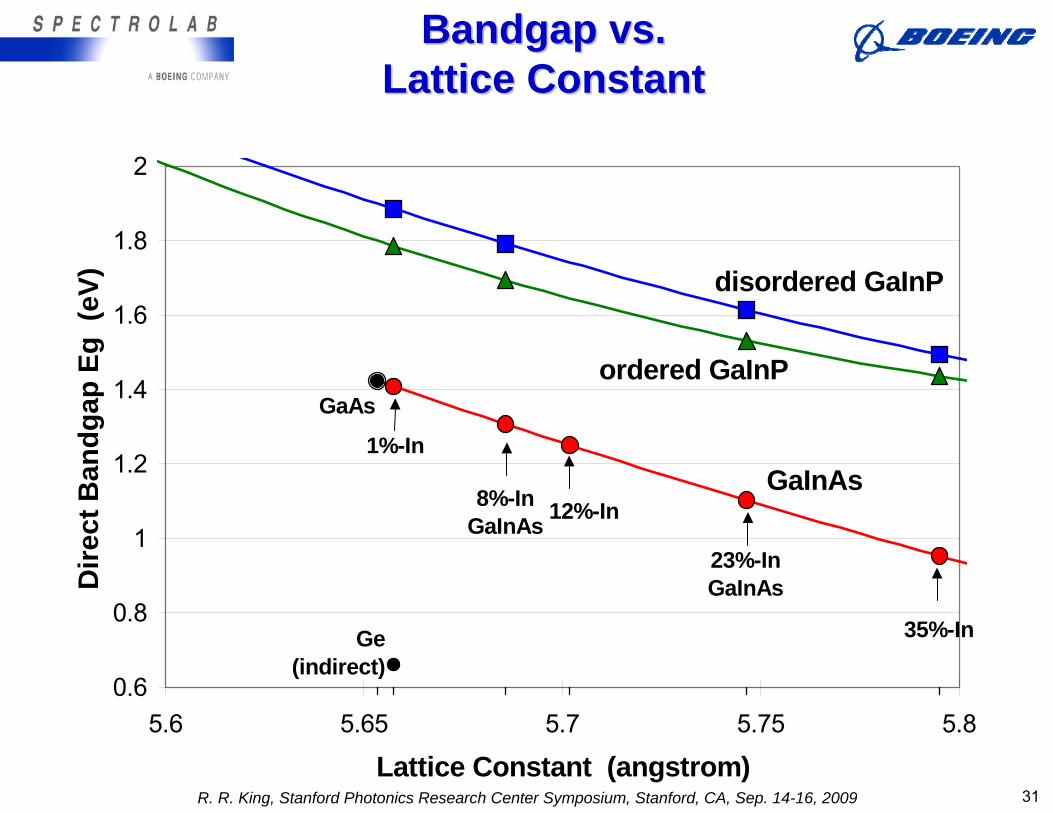
Bandgap vs. Bandgap vs. Lattice ConstantLattice Constant
R. R. King, Stanford Photonics Research Center Symposium, Stanford, CA, Sep. 14-16, 2009 30
Courtesy J. Geisz – NREL
0.6
0.8
1
1.2
1.4
1.6
1.8
2
5.6 5.65 5.7 5.75 5.8
Lattice Constant (angstrom)
Dire
ct B
andg
ap E
g (e
V)
Ge(indirect)
GaAs
disordered GaInP
ordered GaInP
GaInAs8%-In
GaInAs 12%-In
23%-In GaInAs
1%-In
35%-In
Bandgap vs. Bandgap vs. Lattice ConstantLattice Constant
R. R. King, Stanford Photonics Research Center Symposium, Stanford, CA, Sep. 14-16, 2009 31
0
10
20
30
40
50
60
70
80
90
100
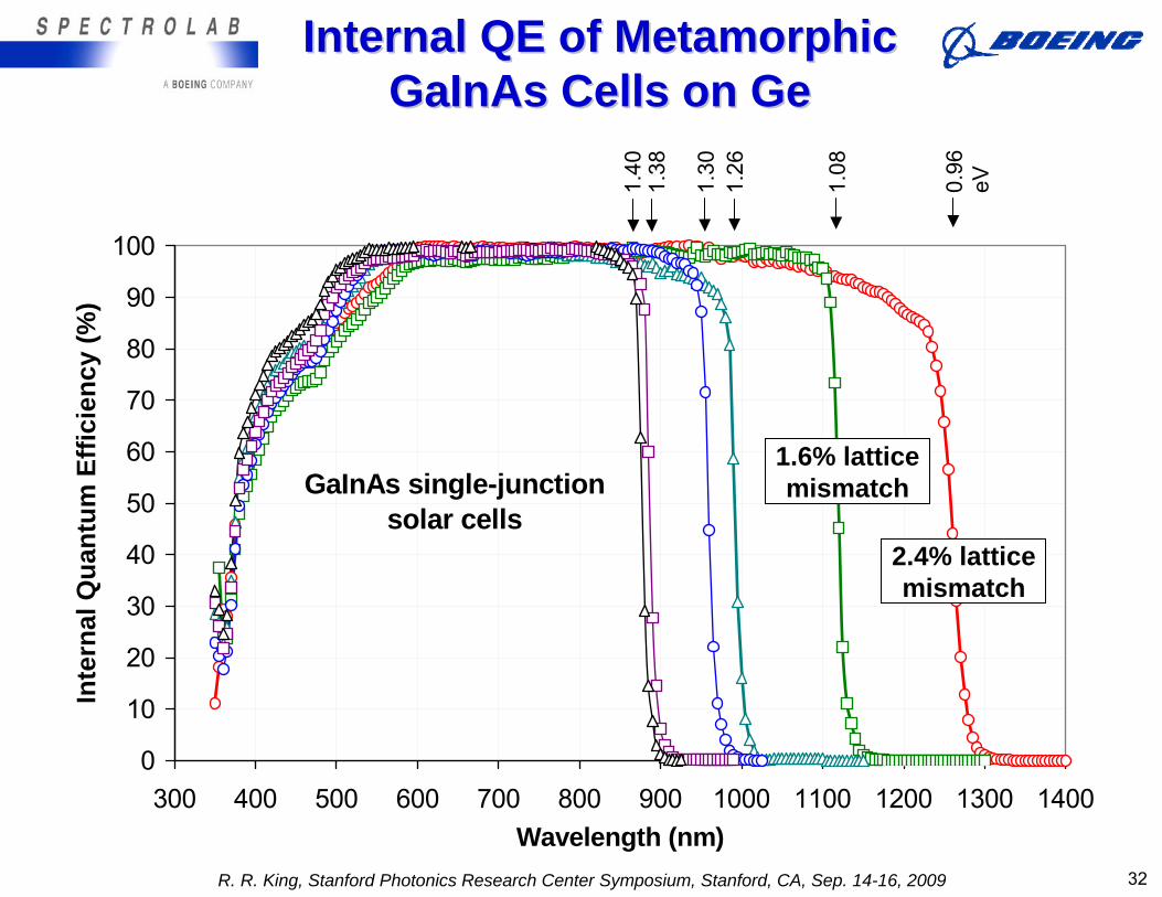
300 400 500 600 700 800 900 1000 1100 1200 1300 1400Wavelength (nm)
Inte
rnal
Qua
ntum
Effi
cien
cy (%
)
0.96
eV1.40
1.08
1.26
1.38
1.30
GaInAs single-junction solar cells
2.4% lattice mismatch
1.6% lattice mismatch
Internal QE of Metamorphic Internal QE of Metamorphic GaInAs Cells on GeGaInAs Cells on Ge
R. R. King, Stanford Photonics Research Center Symposium, Stanford, CA, Sep. 14-16, 2009 32
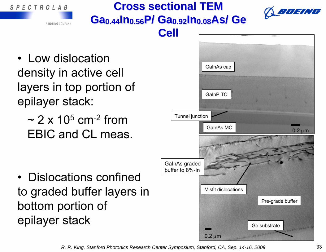
• Low dislocation density in active cell layers in top portion of epilayer stack:
~ 2 x 105 cm-2 from EBIC and CL meas.
• Dislocations confined to graded buffer layers in bottom portion of epilayer stack
GaInAs cap
GaInAs MC
GaInP TC
0.2 μm
Tunnel junction
Pre-grade buffer
Misfit dislocations
GaInAs gradedbuffer to 8%-In
0.2 μm
Ge substrate
Cross sectional TEMCross sectional TEMGaGa0.440.44InIn0.560.56P/ GaP/ Ga0.920.92InIn0.080.08As/ Ge As/ Ge
CellCell
R. R. King, Stanford Photonics Research Center Symposium, Stanford, CA, Sep. 14-16, 2009 33
Line of 0%relaxation
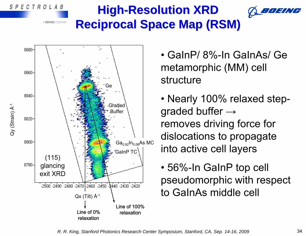
Line of 100%relaxation
Qy
(Stra
in) Å
-1
Qx (Tilt) Å-1
Ge
Ga0.92In0.08As MC
GaInP TC
GradedBuffer
(115) glancing exit XRD
Line of 0%relaxation
Line of 100%relaxation
Qy
(Stra
in) Å
-1
Qx (Tilt) Å-1
Ge
Ga0.92In0.08As MC
GaInP TC
GradedBuffer
(115) glancing exit XRD
• GaInP/ 8%-In GaInAs/ Ge metamorphic (MM) cell structure
• Nearly 100% relaxed step-graded buffer →removes driving force for dislocations to propagate into active cell layers
• 56%-In GaInP top cell pseudomorphic with respect to GaInAs middle cell
HighHigh--Resolution XRD Resolution XRD Reciprocal Space Map (RSM)Reciprocal Space Map (RSM)
R. R. King, Stanford Photonics Research Center Symposium, Stanford, CA, Sep. 14-16, 2009 34
Ge or GaAs substrate
Growth on Ge or GaAs substrate, followed by substrate removal from sunward surface
nucleation
buffer layerbuffer layer
emitter
1.39-eV GaInAsinverted LM subcell
base
contact
metal
hν
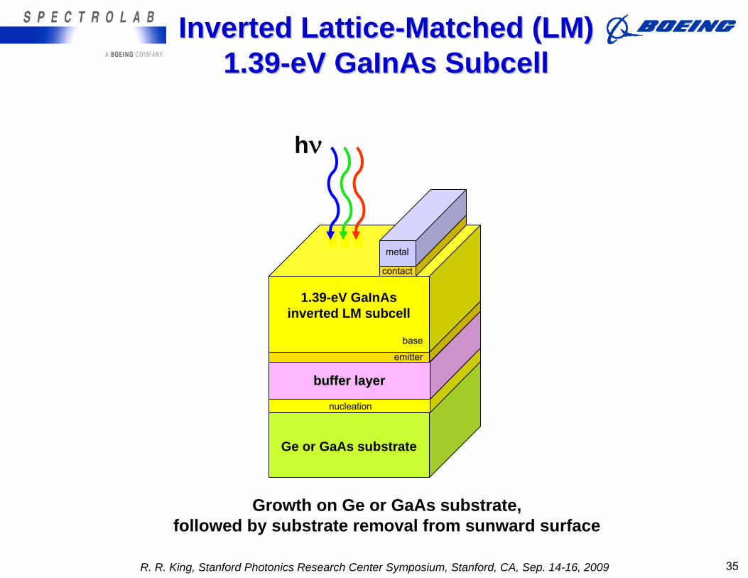
Inverted LatticeInverted Lattice--Matched (LM)Matched (LM)1.391.39--eV GaInAs SubcelleV GaInAs Subcell
R. R. King, Stanford Photonics Research Center Symposium, Stanford, CA, Sep. 14-16, 2009 35
Ge substrate
Growth on Ge or GaAs substrate, followed by substrate removal from sunward surface
nucleation and pre-grade buffer
transparent MM transparent MM graded buffer layersgraded buffer layers
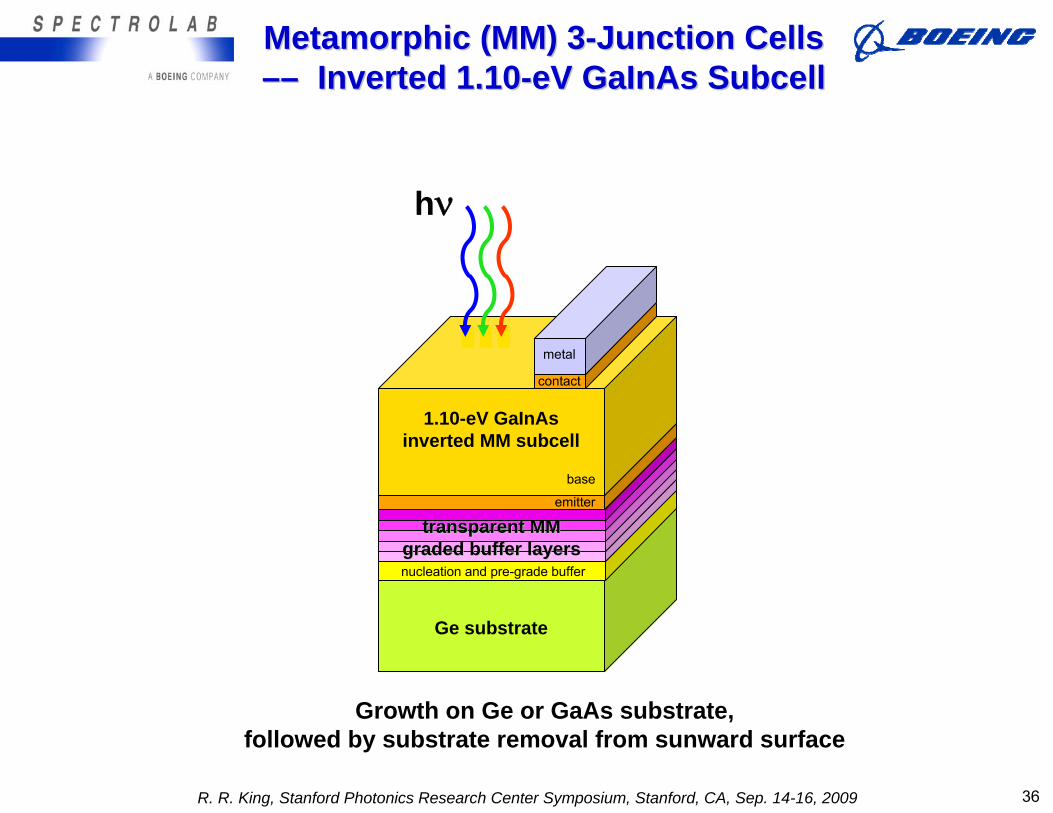
emitter
1.10-eV GaInAsinverted MM subcell
base
contact
metal
hν
Metamorphic (MM) 3Metamorphic (MM) 3--Junction Cells Junction Cells –––– Inverted 1.10Inverted 1.10--eV GaInAs SubcelleV GaInAs Subcell
R. R. King, Stanford Photonics Research Center Symposium, Stanford, CA, Sep. 14-16, 2009 36
Ge substrate
Growth on Ge or GaAs substrate, followed by substrate removal from sunward surface
nucleation and pre-grade buffer
transparent MM transparent MM graded buffer layersgraded buffer layers
emitteremitter
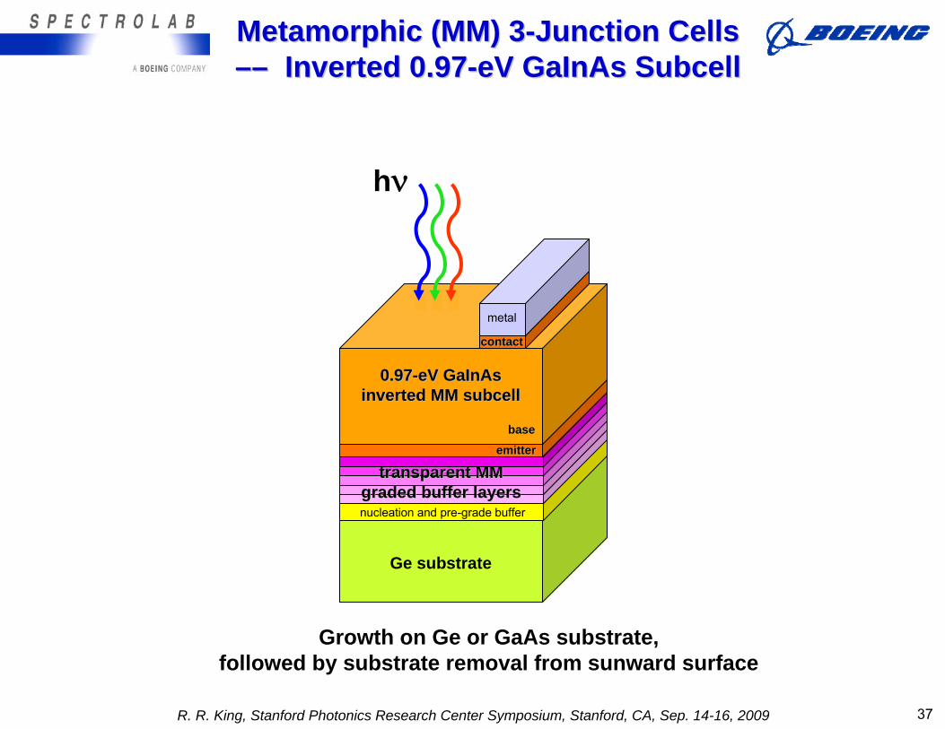
0.970.97--eV GaInAseV GaInAsinverted MM subcellinverted MM subcell
basebase
contactcontact
metal
hν
Metamorphic (MM) 3Metamorphic (MM) 3--Junction Cells Junction Cells –––– Inverted 0.97Inverted 0.97--eV GaInAs SubcelleV GaInAs Subcell
R. R. King, Stanford Photonics Research Center Symposium, Stanford, CA, Sep. 14-16, 2009 37
Ge substrate
Growth on Ge or GaAs substrate, followed by substrate removal from sunward surface
nucleation and pre-grade buffer
transparent MM transparent MM graded buffer layersgraded buffer layers
emitteremitter
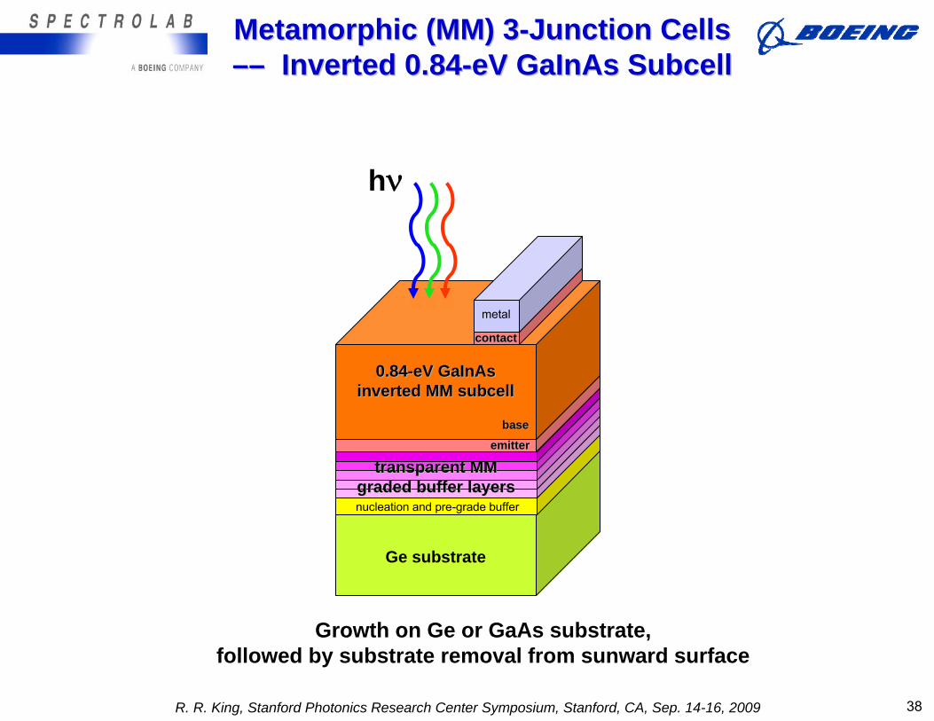
0.840.84--eV GaInAseV GaInAsinverted MM subcellinverted MM subcell
basebase
contactcontact
metal
hν
Metamorphic (MM) 3Metamorphic (MM) 3--Junction Cells Junction Cells –––– Inverted 0.84Inverted 0.84--eV GaInAs SubcelleV GaInAs Subcell
R. R. King, Stanford Photonics Research Center Symposium, Stanford, CA, Sep. 14-16, 2009 38
Ge or GaAs substrateGe or GaAs substrate
nucleationnucleation
buffer layerbuffer layerbuffer layerbuffer layer
emitter
1.39-eV GaInAsinverted LM subcell
base
emitter
1.39-eV GaInAsinverted LM subcell
base
contactcontact
metalmetal
50 μm8e-9766-1
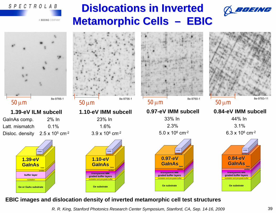
1.39-eV ILM subcellGaInAs comp. 2% InLatt. mismatch 0.1%Disloc. density 2.5 x 105 cm-2
50 μm8e-9756-1
50 μm8e-9760-1
50 μm8e-9783-11
EBIC images and dislocation density of inverted metamorphic cell test structures
1.391.39--eV eV GaInAsGaInAs
1.10-eV IMM subcell23% In1.6%
3.9 x 106 cm-2
0.97-eV IMM subcell33% In2.3%
5.0 x 106 cm-2
0.84-eV IMM subcell44% In3.1%
6.3 x 106 cm-2
Ge substrateGe substrate
nucleation and pre-grade buffernucleation and pre-grade buffer
transparent MM transparent MM graded buffer layersgraded buffer layers
transparent MM transparent MM graded buffer layersgraded buffer layers
emitter
1.10-eV GaInAsinverted MM subcell
base
emitter
1.10-eV GaInAsinverted MM subcell
base
contactcontact
metalmetal
1.101.10--eV eV GaInAsGaInAs
Ge substrateGe substrate
nucleation and pre-grade buffernucleation and pre-grade buffer
transparent MM transparent MM graded buffer layersgraded buffer layers
transparent MM transparent MM graded buffer layersgraded buffer layers
emitteremitter
0.970.97--eV GaInAseV GaInAsinverted MM subcellinverted MM subcell
basebase
emitteremitter
0.970.97--eV GaInAseV GaInAsinverted MM subcellinverted MM subcell
basebase
contactcontactcontactcontact
metalmetal
0.970.97--eV eV GaInAsGaInAs
Ge substrateGe substrate
nucleation and pre-grade buffernucleation and pre-grade buffer
transparent MM transparent MM graded buffer layersgraded buffer layers
transparent MM transparent MM graded buffer layersgraded buffer layers
emitteremitter
0.840.84--eV GaInAseV GaInAsinverted MM subcellinverted MM subcell
basebase
emitteremitter
0.840.84--eV GaInAseV GaInAsinverted MM subcellinverted MM subcell
basebase
contactcontactcontactcontact
metalmetal
0.840.84--eV eV GaInAsGaInAs
Dislocations in Inverted Dislocations in Inverted Metamorphic Cells Metamorphic Cells –– EBICEBIC
R. R. King, Stanford Photonics Research Center Symposium, Stanford, CA, Sep. 14-16, 2009 39
0.0
0.2
0.4
0.6
0.8
1.0
1.2
1.4
0 10 20 30 40 50In Composition for GaxIn1-xAs (%)
Ban
d G
ap E
g, O
pen-
Circ
uit V
olta
ge V
oc,
and
Ban
d G
ap-V
olta
ge O
ffset
(V
)
0
1
2
3
4
5
6
7
8
Dis
loca
tion
Den
sity
from
EB
IC (
106 c
m-2
)
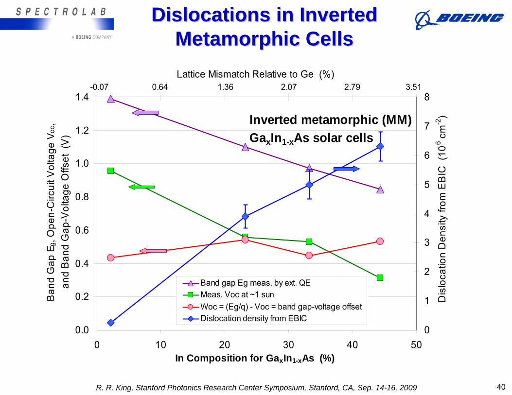
Band gap Eg meas. by ext. QEMeas. Voc at ~1 sunWoc = (Eg/q) - Voc = band gap-voltage offsetDislocation density from EBIC
-0.07 0.64 1.36 2.07 2.79 3.51Lattice Mismatch Relative to Ge (%)
Inverted metamorphic (MM)GaxIn1-xAs solar cells
Dislocations in Inverted Dislocations in Inverted Metamorphic CellsMetamorphic Cells
R. R. King, Stanford Photonics Research Center Symposium, Stanford, CA, Sep. 14-16, 2009 40
0
1
2
3
4
5
6
7
8
9
0 10 20 30 40 50In Composition for GaxIn1-xAs (%)
Dis
loca
tion
Den
sity
from
EB
IC (
106 c
m-2
)an
d P
hoto
n In
tens
ity fr
om C
L (1
0 3 c
ps)
0
5
10
15
20
25
30
35
40
45
50
Car
rier L
oss
(%)
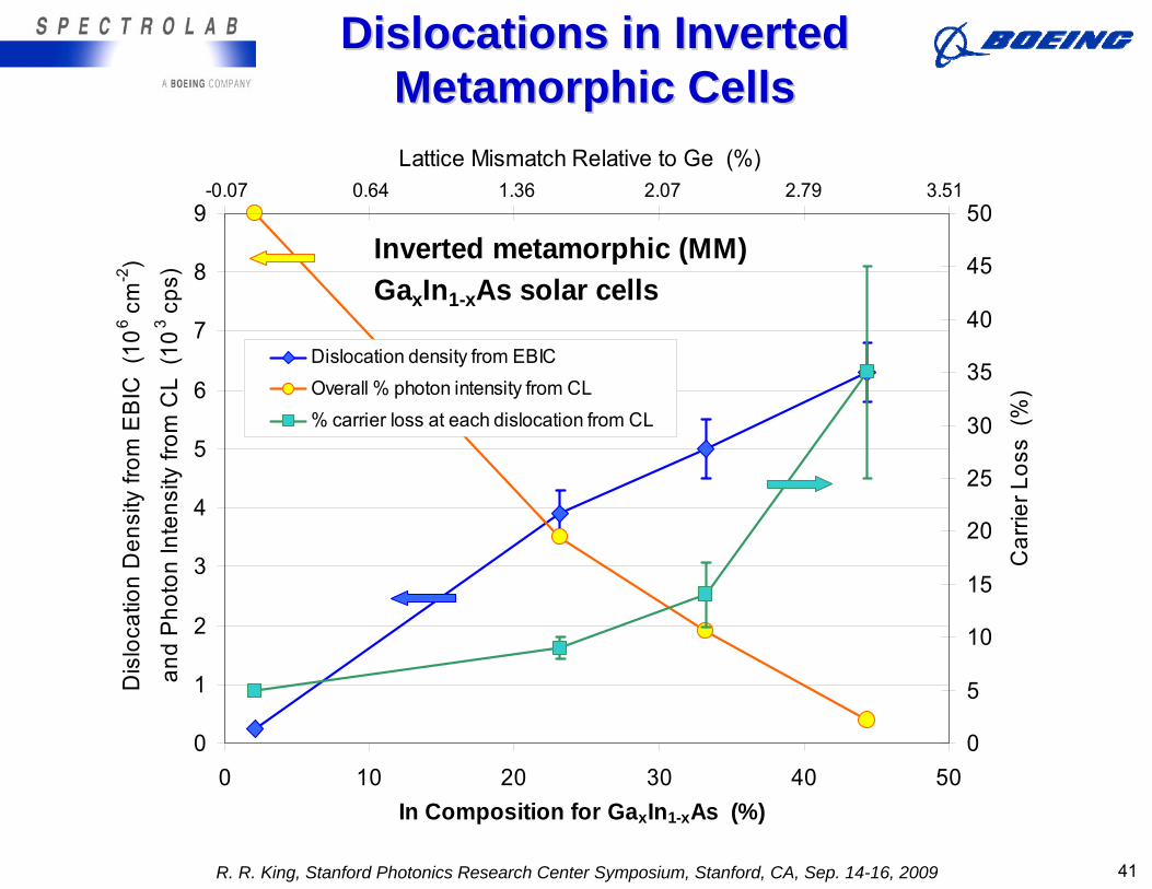
Dislocation density from EBICOverall % photon intensity from CL% carrier loss at each dislocation from CL
-0.07 0.64 1.36 2.07 2.79 3.51Lattice Mismatch Relative to Ge (%)
Inverted metamorphic (MM)GaxIn1-xAs solar cells
Dislocations in Inverted Dislocations in Inverted Metamorphic CellsMetamorphic Cells
R. R. King, Stanford Photonics Research Center Symposium, Stanford, CA, Sep. 14-16, 2009 41
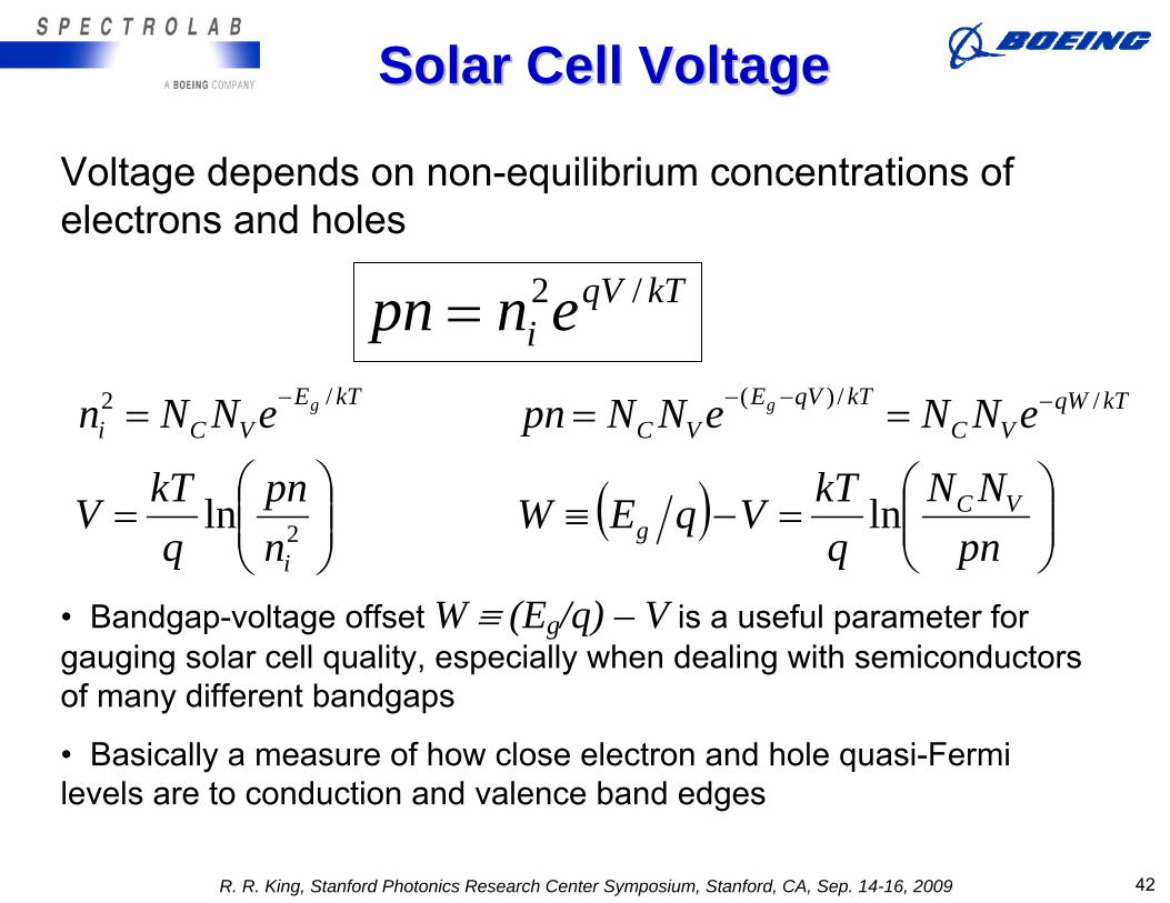
Voltage depends on non-equilibrium concentrations of electrons and holes
kTqVi enpn /2=
( ) ⎟⎟⎠
⎞⎜⎜⎝
⎛=−≡⎟⎟
⎠
⎞⎜⎜⎝
⎛=
=== −−−−
pnNN
qkTVqEW
npn
qkTV
eNNeNNpn eNNn
VCg
i
kTqWVC
kTqVEVC
kTEVCi
gg
lnln 2
//)(/2
• Bandgap-voltage offset W ≡ (Eg/q) – V is a useful parameter for gauging solar cell quality, especially when dealing with semiconductors of many different bandgaps
• Basically a measure of how close electron and hole quasi-Fermi levels are to conduction and valence band edges
Solar Cell VoltageSolar Cell Voltage
R. R. King, Stanford Photonics Research Center Symposium, Stanford, CA, Sep. 14-16, 2009 42
0.0
0.5
1.0
1.5
2.0
0.6 1 1.4 1.8 2.2Bandgap Eg (eV)
Eg/q
, Voc
, and
(Eg/
q) -
Voc
(V)
VocEg from EQE(Eg/q) - Vocradiative limit
d-A
lGaI
nP
GaA
s1.
4 - e
V G
aInA
s
o-G
aInP
AlG
aInA
s
d-A
lGaI
nPd-
GaI
nP
d-A
lGaI
nP
0.97
-eV
GaI
nAs
GaI
nNA
s
1.10
-eV
GaI
nAs
1.24
-eV
GaI
nAs
1.30
-eV
GaI
nAs
Ge
(ind
irect
gap
)
AlG
aInA
s
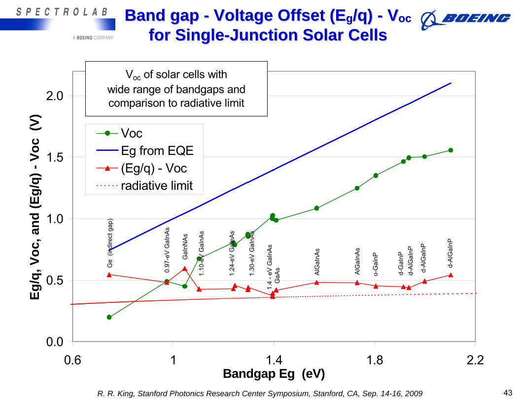
Voc of solar cells with wide range of bandgaps and comparison to radiative limit
Band gap Band gap -- Voltage Offset (EVoltage Offset (Egg/q) /q) -- VVococfor Singlefor Single--Junction Solar CellsJunction Solar Cells
R. R. King, Stanford Photonics Research Center Symposium, Stanford, CA, Sep. 14-16, 2009 43
0.0
0.5
1.0
1.5
2.0
0.6 1 1.4 1.8 2.2 2.6 3Bandgap Eg (eV)
Eg/q
, Voc
, and
(Eg/
q) -
Voc
(V)
0
100
200
300
400
500
600
700
800
Inte
nsity
per
Uni
t Pho
ton
Ener
gy (
W/(m
2 . eV
))
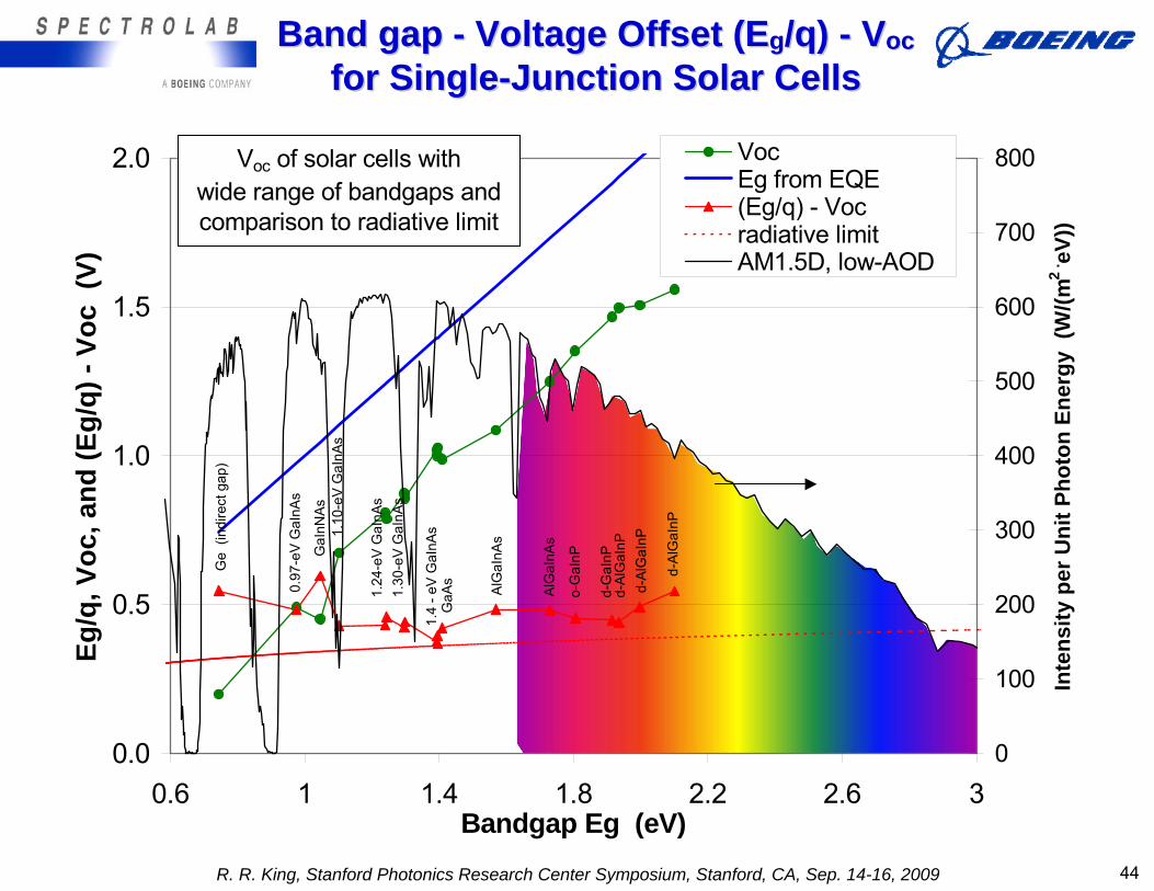
VocEg from EQE(Eg/q) - Vocradiative limitAM1.5D, low-AOD
Voc of solar cells with wide range of bandgaps and comparison to radiative limit
d-A
lGaI
nP
GaA
s1.
4 - e
V G
aInA
s
o-G
aInP
AlG
aInA
s
d-A
lGaI
nPd-
GaI
nP
d-A
lGaI
nP
0.97
-eV
GaI
nAs
GaI
nNA
s1.
10-e
V G
aInA
s
1.24
-eV
GaI
nAs
1.30
-eV
GaI
nAs
Ge
(ind
irect
gap
)
AlG
aInA
s
Band gap Band gap -- Voltage Offset (EVoltage Offset (Egg/q) /q) -- VVococfor Singlefor Single--Junction Solar CellsJunction Solar Cells
R. R. King, Stanford Photonics Research Center Symposium, Stanford, CA, Sep. 14-16, 2009 44
High-Efficiency
Multijunction Cells
R. R. King, Stanford Photonics Research Center Symposium, Stanford, CA, Sep. 14-16, 2009 45
Tunnel Ju
nction
Top Cell
Wide-Eg Tunnel
Middle Cell
p-GaInP BSF
p-GaInP base
n-Ga(In)As emitter
n+-Ge emitter
p-AlGaInP BSF
n-GaInP emittern-AlInP windown+-Ga(In)As
contact
AR
p-Ge baseand substratecontact
n-Ga(In)As buffer
Bottom Cell
p++-TJn++-TJ
p-Ga(In)As base
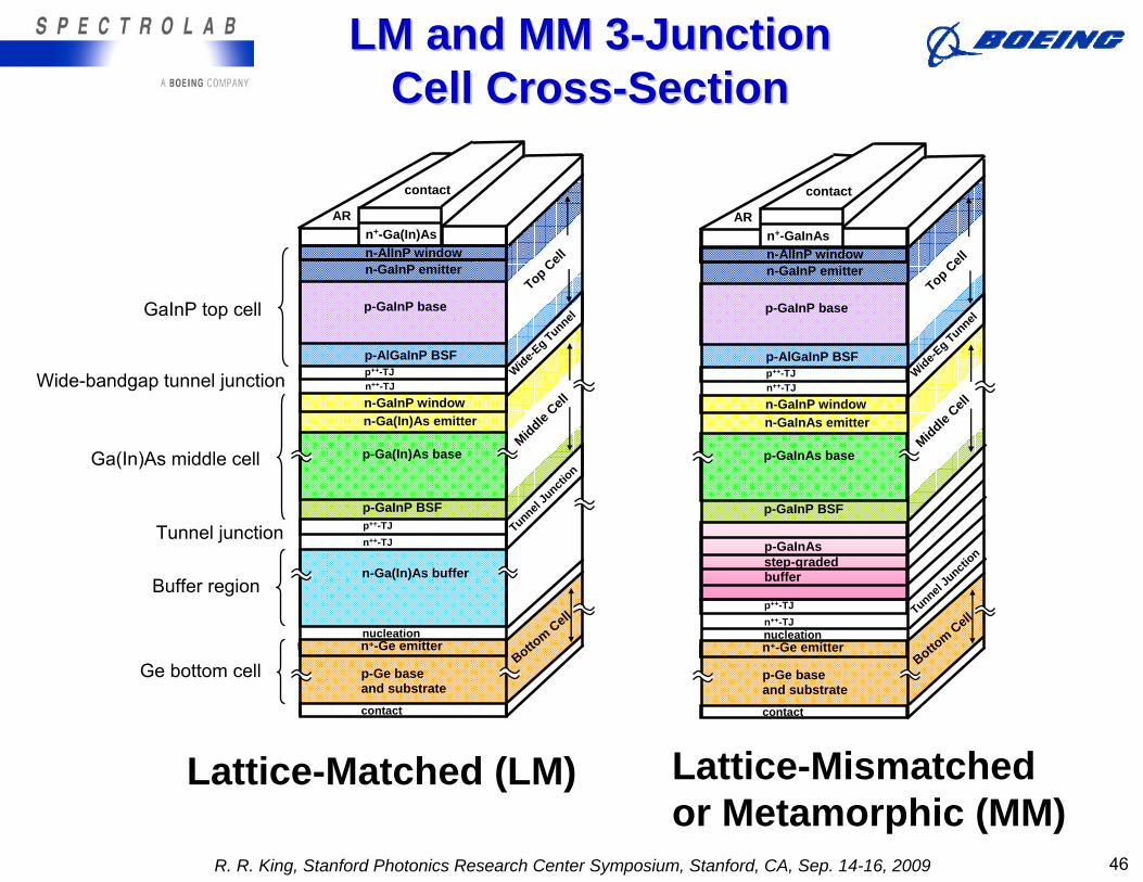
nucleation
Wide-bandgap tunnel junction
GaInP top cell
Ge bottom cell
n-GaInP window
p++-TJn++-TJ
Ga(In)As middle cell
Tunnel junction
Buffer regionTunnel
Juncti
on
Top Cell
Wide-Eg Tunnel
Middle Cell
p-GaInP BSF
p-GaInP base
n-GaInAs emitter
n+-Ge emitter
p-AlGaInP BSF
n-GaInP emittern-AlInP windown+-GaInAs
contact
AR
p-Ge baseand substratecontact
p-GaInAsstep-graded buffer
Bottom Cell
p++-TJn++-TJ
p-GaInAs base
nucleation
n-GaInP window
p++-TJn++-TJ
Lattice-Matched (LM) Lattice-Mismatchedor Metamorphic (MM)
LM and MM 3LM and MM 3--Junction Junction Cell CrossCell Cross--SectionSection
R. R. King, Stanford Photonics Research Center Symposium, Stanford, CA, Sep. 14-16, 2009 46
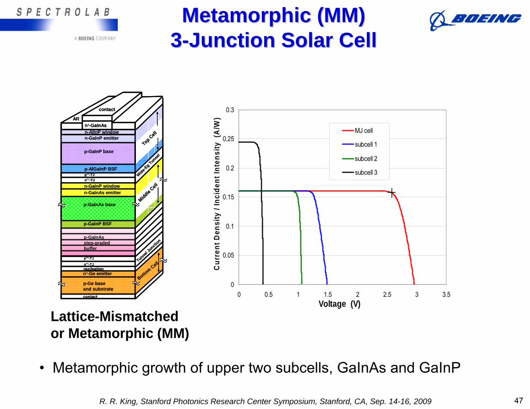
Metamorphic (MM) Metamorphic (MM) 33--Junction Solar CellJunction Solar Cell
Tunnel Ju
nction
Top Cell
Wide-Eg Tunnel
Middle Cell
p-GaInP BSF
p-GaInP base
n-GaInAs emitter
n+-Ge emitter
p-AlGaInP BSF
n-GaInP emittern-AlInP windown+-GaInAs
contact
AR
p-Ge baseand substratecontact
p-GaInAsstep-graded buffer
Bottom Cell
p++-TJn++-TJ
p-GaInAs base
nucleation
n-GaInP window
p++-TJn++-TJ
Lattice-Mismatchedor Metamorphic (MM)
0
0.05
0.1
0.15
0.2
0.25
0.3
0 0.5 1 1.5 2 2.5 3 3.5Voltage (V)
Cur
rent
Den
sity
/ In
cide
nt In
tens
ity (
A/W
)
MJ cell
subcell 1
subcell 2
subcell 3
• Metamorphic growth of upper two subcells, GaInAs and GaInP
R. R. King, Stanford Photonics Research Center Symposium, Stanford, CA, Sep. 14-16, 2009 47
0
10
20
30
40
50
60
70
80
90
100
300 500 700 900 1100 1300 1500 1700 1900
Wavelength (nm)
Cur
rent
Den
sity
per
Uni
t W
avel
engt
h (m
A/(c
m2 μ
m))
0
10
20
30
40
50
60
70
80
90
100
Exte
rnal
Qua
ntum
Effi
cien
cy (
%)
AM1.5D, low-AODAM1.5G, ASTM G173-03
AM0, ASTM E490-00aEQE, lattice-matched
EQE, metamorphic
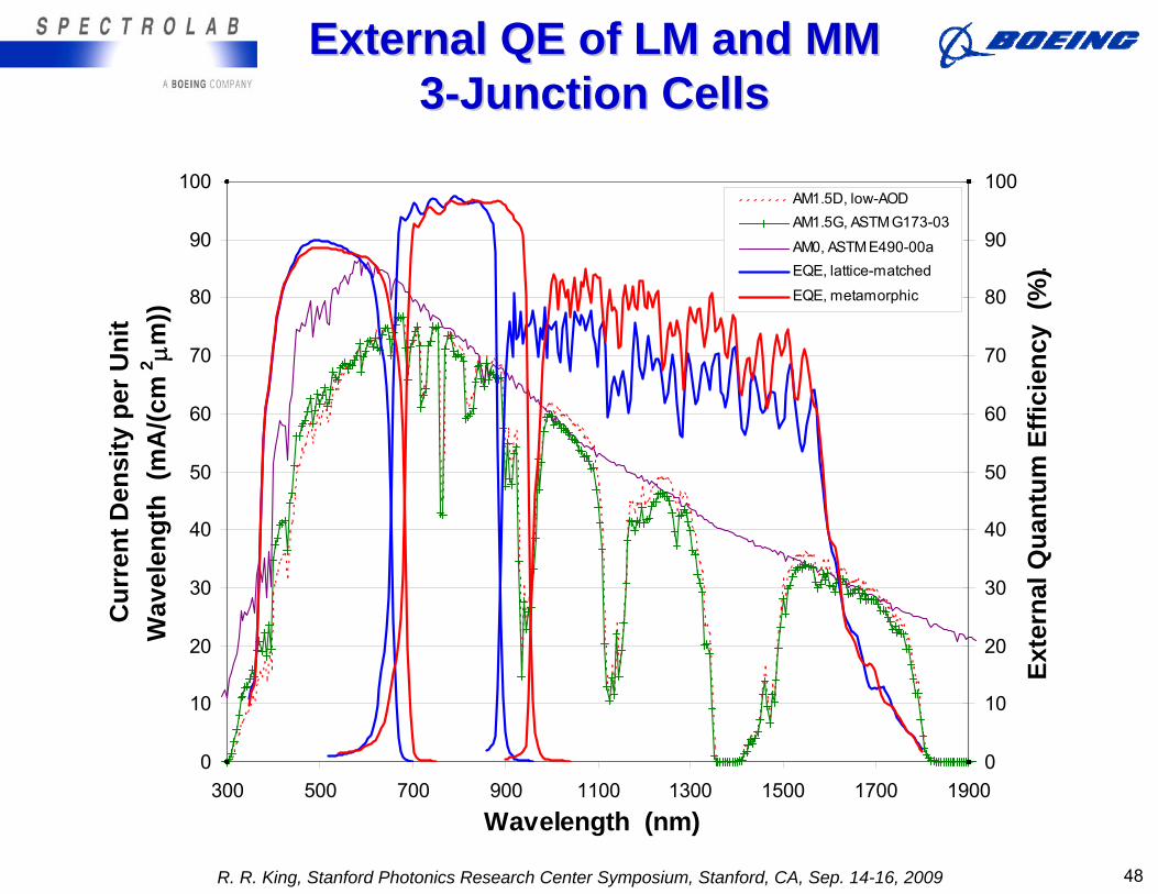
External QE of LM and MM External QE of LM and MM 33--Junction CellsJunction Cells
R. R. King, Stanford Photonics Research Center Symposium, Stanford, CA, Sep. 14-16, 2009 48
1.3
1.4
1.5
1.6
1.7
1.8
1.9
2
2.1
1.0 1.1 1.2 1.3 1.4 1.5 1.6
Eg2 = Subcell 2 Bandgap (eV)
E g1 =
Sub
cell
1 (T
op) B
andg
ap (
eV)
.
Disordered GaInP top subcell Ordered GaInP top subcell
38%
54%
42%
46%
50%
52%
3-junction Eg1/ Eg2/ 0.67 eV cell efficiency240 suns (24.0 W/cm2), AM1.5D (ASTM G173-03), 25oCIdeal efficiency -- radiative recombination limit
40.7% 40.1%
48%
44%
40%
MMLM
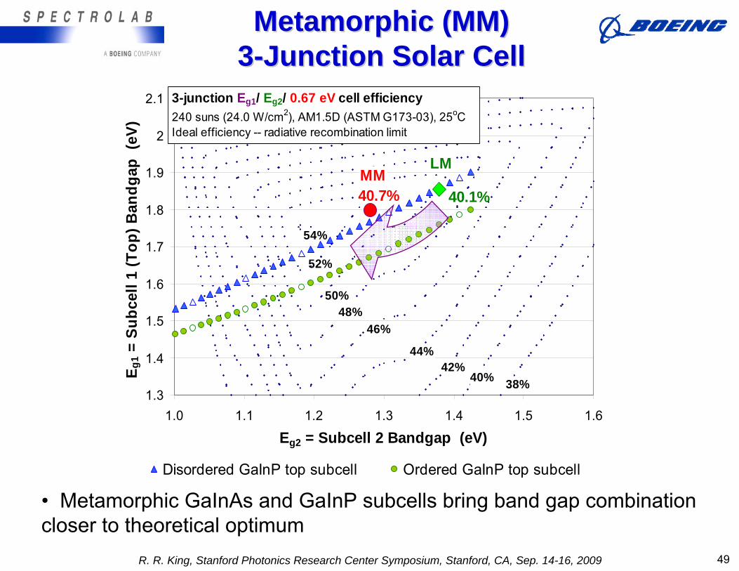
Metamorphic (MM) Metamorphic (MM) 33--Junction Solar CellJunction Solar Cell
• Metamorphic GaInAs and GaInP subcells bring band gap combination closer to theoretical optimum
R. R. King, Stanford Photonics Research Center Symposium, Stanford, CA, Sep. 14-16, 2009 49
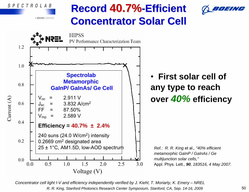
Concentrator cell light I-V and efficiency independently verified by J. Kiehl, T. Moriarty, K. Emery – NREL
• First solar cell of any type to reach over 40% efficiency
SpectrolabMetamorphic
GaInP/ GaInAs/ Ge CellVoc = 2.911 V Jsc = 3.832 A/cm2
FF = 87.50%Vmp = 2.589 V
Efficiency = 40.7% ± 2.4% 240 suns (24.0 W/cm2) intensity0.2669 cm2 designated area25 ± 1°C, AM1.5D, low-AOD spectrum Ref.: R. R. King et al., "40% efficient
metamorphic GaInP / GaInAs / Ge multijunction solar cells," Appl. Phys. Lett., 90, 183516, 4 May 2007.
Record Record 40.7%40.7%--Efficient Efficient Concentrator Solar CellConcentrator Solar Cell
R. R. King, Stanford Photonics Research Center Symposium, Stanford, CA, Sep. 14-16, 2009 50
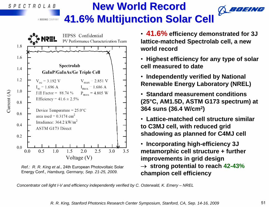
New World RecordNew World Record41.6% Multijunction Solar Cell41.6% Multijunction Solar Cell
• 41.6% efficiency demonstrated for 3J lattice-matched Spectrolab cell, a new world record• Highest efficiency for any type of solar cell measured to date• Independently verified by National Renewable Energy Laboratory (NREL)• Standard measurement conditions (25°C, AM1.5D, ASTM G173 spectrum) at 364 suns (36.4 W/cm2)• Lattice-matched cell structure similar to C3MJ cell, with reduced grid shadowing as planned for C4MJ cell• Incorporating high-efficiency 3J metamorphic cell structure + further improvements in grid design → strong potential to reach 42-43%champion cell efficiency
Ref.: R. R. King et al., 24th European Photovoltaic Solar Energy Conf., Hamburg, Germany, Sep. 21-25, 2009.
Concentrator cell light I-V and efficiency independently verified by C. Osterwald, K. Emery – NREL
R. R. King, Stanford Photonics Research Center Symposium, Stanford, CA, Sep. 14-16, 2009 51
24
26
28
30
32
34
36
38
40
42
44
0.1 1.0 10.0 100.0 1000.0
Incident Intensity (suns) (1 sun = 0.100 W/cm2)
Effic
ienc
y (%
) and
Voc
x 1
0 (V
)
0.78
0.80
0.82
0.84
0.86
0.88
0.90
0.92
0.94
0.96
0.98
Fill
Fact
or (
unitl
ess)
Efficiency
Voc x 10
Voc fit, 100 to 1000 suns
FF
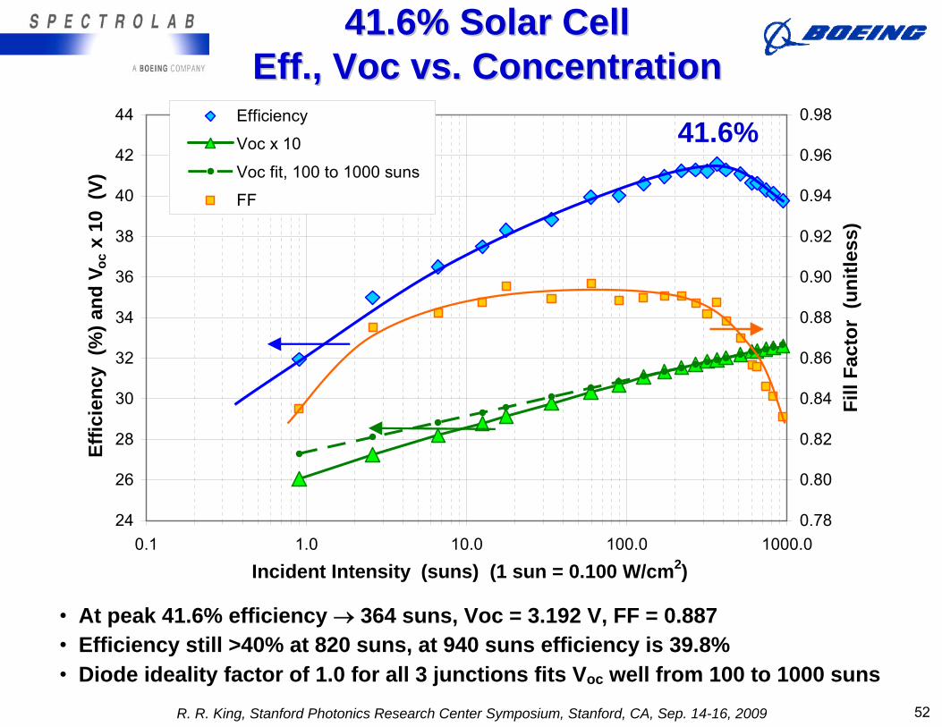
• At peak 41.6% efficiency → 364 suns, Voc = 3.192 V, FF = 0.887• Efficiency still >40% at 820 suns, at 940 suns efficiency is 39.8%• Diode ideality factor of 1.0 for all 3 junctions fits Voc well from 100 to 1000 suns
41.6% Solar Cell41.6% Solar CellEff., Voc vs. ConcentrationEff., Voc vs. Concentration
41.6%
R. R. King, Stanford Photonics Research Center Symposium, Stanford, CA, Sep. 14-16, 2009 52
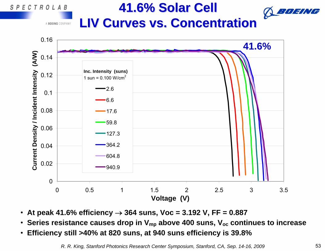
• At peak 41.6% efficiency → 364 suns, Voc = 3.192 V, FF = 0.887• Series resistance causes drop in Vmp above 400 suns, Voc continues to increase• Efficiency still >40% at 820 suns, at 940 suns efficiency is 39.8%
41.6% Solar Cell41.6% Solar CellLIV Curves vs. ConcentrationLIV Curves vs. Concentration
0
0.02
0.04
0.06
0.08
0.1
0.12
0.14
0.16
0 0.5 1 1.5 2 2.5 3 3.5Voltage (V)
Cur
rent
Den
sity
/ In
cide
nt In
tens
ity (
A/W
)
2.6
6.6
17.6
59.8
127.3
364.2
604.8
940.9
Inc. Intensity (suns)1 sun = 0.100 W/cm2
41.6%
R. R. King, Stanford Photonics Research Center Symposium, Stanford, CA, Sep. 14-16, 2009 53
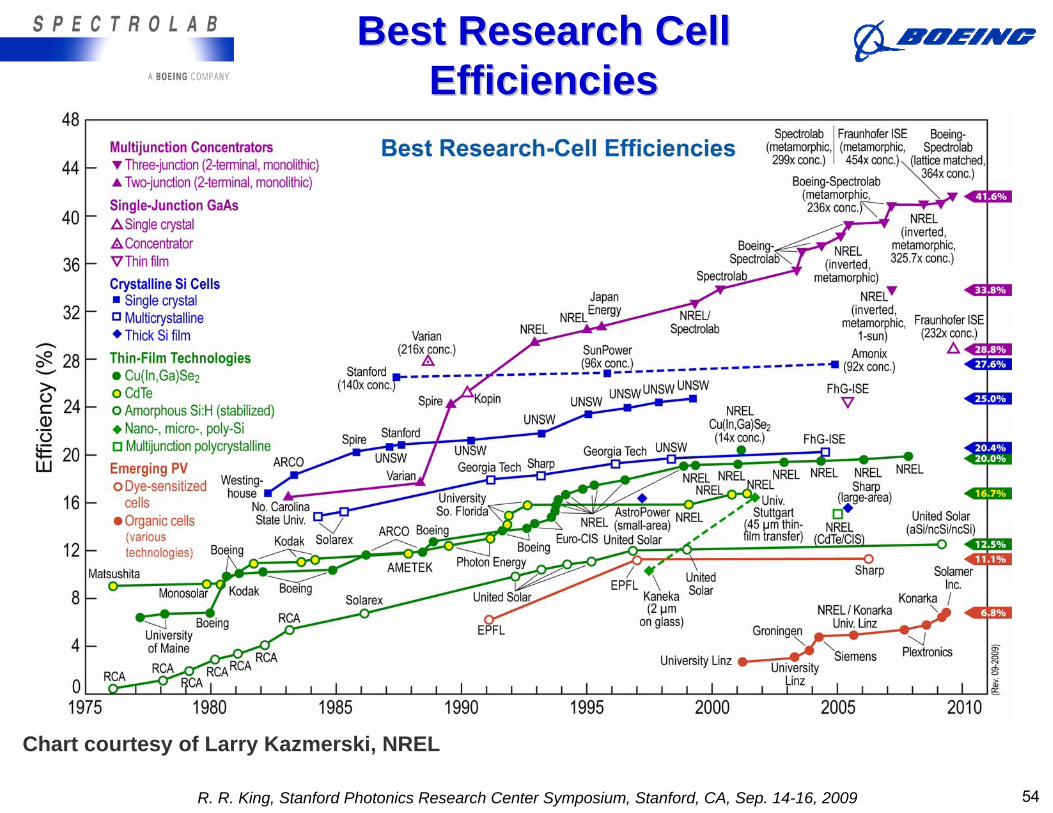
Chart courtesy of Larry Kazmerski, NREL
Best Research Cell Best Research Cell EfficienciesEfficiencies
R. R. King, Stanford Photonics Research Center Symposium, Stanford, CA, Sep. 14-16, 2009 54
Growth on Ge or GaAs substrate, followed by substrate removal from
sunward surface
GrowthDirection
cap
1.9 eV (Al)GaInP subcell 1
1.4 eV GaInAs subcell 2
graded MM buffer layers
1.0 eV GaInAs subcell 3
cap
1.9 eV (Al)GaInP subcell 1
1.4 eV GaInAs subcell 2
graded MM buffer layers
1.0 eV GaInAs subcell 3
Ge or GaAs substrateGe or GaAs substrate
Ge or GaAs substrate
cap
Ge or GaAs substrateGe or GaAs substrate
capcap
0
0.02
0.04
0.06
0.08
0.1
0.12
0.14
0.16
0 0.5 1 1.5 2 2.5 3 3.5 4Voltage (V)
Cur
rent
Den
sity
/ In
cide
nt In
tens
ity (
A/W
)
MJ cell
subcell 1
subcell 2
subcell 3
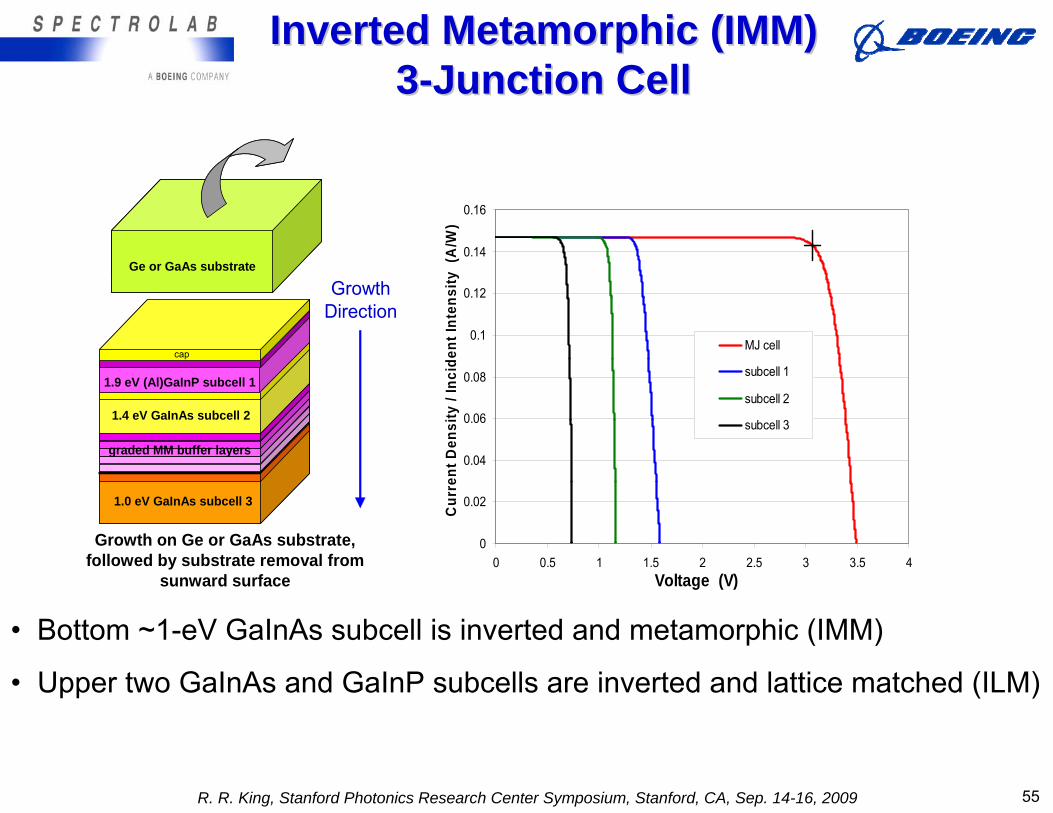
Inverted Metamorphic (IMM) Inverted Metamorphic (IMM) 33--Junction CellJunction Cell
• Bottom ~1-eV GaInAs subcell is inverted and metamorphic (IMM)
• Upper two GaInAs and GaInP subcells are inverted and lattice matched (ILM)
R. R. King, Stanford Photonics Research Center Symposium, Stanford, CA, Sep. 14-16, 2009 55
1
1.1
1.2
1.3
1.4
1.5
1.6
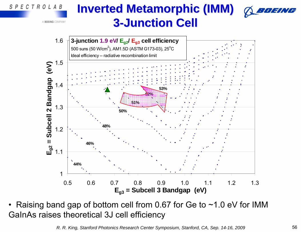
0.5 0.6 0.7 0.8 0.9 1.0 1.1 1.2 1.3Eg3 = Subcell 3 Bandgap (eV)
E g2 =
Sub
cell
2 B
andg
ap (
eV)
.
48%
53%
44%
46%
50%
52%
3-junction 1.9 eV/ Eg2/ Eg3 cell efficiency500 suns (50 W/cm2), AM1.5D (ASTM G173-03), 25oCIdeal efficiency -- radiative recombination limitX
51%
Inverted Metamorphic (IMM) Inverted Metamorphic (IMM) 33--Junction CellJunction Cell
• Raising band gap of bottom cell from 0.67 for Ge to ~1.0 eV for IMM GaInAs raises theoretical 3J cell efficiency
R. R. King, Stanford Photonics Research Center Symposium, Stanford, CA, Sep. 14-16, 2009 56
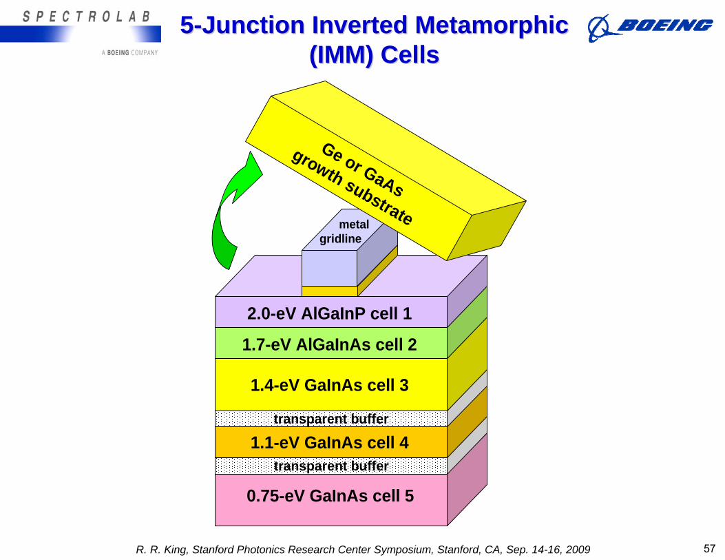
55--Junction Inverted Metamorphic Junction Inverted Metamorphic (IMM) Cells(IMM) Cells
transparent buffer
0.75-eV GaInAs cell 5
1.1-eV GaInAs cell 4transparent buffer
1.4-eV GaInAs cell 3
1.7-eV AlGaInAs cell 2
2.0-eV AlGaInP cell 1
metal gridline
Ge or GaAs
growth substrate
R. R. King, Stanford Photonics Research Center Symposium, Stanford, CA, Sep. 14-16, 2009 57
cap
contactAR
(Al)GaInP Cell 1 1.9 eVwide-Eg tunnel junction
AlGa(In)As Cell 21.6 eV
Ga(In)As Cell 31.4 eV
tunnel junction
AR
Ga(In)As buffer
Ge Cell 4and substrate
0.67 eV
nucleation
back contact
wide-Eg tunnel junction
cap
contactAR
(Al)GaInP Cell 1 1.9 eVwide-Eg tunnel junction
AlGa(In)As Cell 21.6 eV
Ga(In)As Cell 31.4 eV
tunnel junction
AR
Ga(In)As buffer
Ge Cell 4and substrate
0.67 eV
nucleationnucleation
back contact
wide-Eg tunnel junction
0
0.05
0.1
0.15
0.2
0.25
0 1 2 3 4 5Voltage (V)
Cur
rent
Den
sity
/ In
cide
nt In
tens
ity (
A/W
)
MJ cell
subcell 1
subcell 2
subcell 3
subcell 4
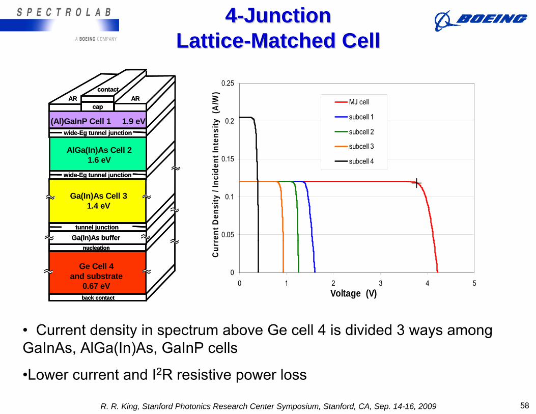
44--Junction Junction LatticeLattice--Matched CellMatched Cell
• Current density in spectrum above Ge cell 4 is divided 3 ways among GaInAs, AlGa(In)As, GaInP cells
•Lower current and I2R resistive power loss
R. R. King, Stanford Photonics Research Center Symposium, Stanford, CA, Sep. 14-16, 2009 58
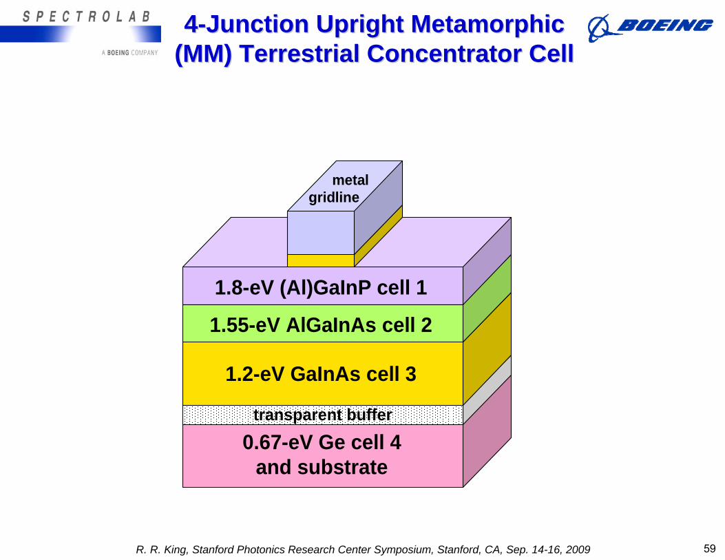
44--Junction Upright Metamorphic Junction Upright Metamorphic (MM) Terrestrial Concentrator Cell(MM) Terrestrial Concentrator Cell
0.67-eV Ge cell 4 and substrate
transparent buffer
1.2-eV GaInAs cell 3
1.55-eV AlGaInAs cell 2
1.8-eV (Al)GaInP cell 1
metal gridline
R. R. King, Stanford Photonics Research Center Symposium, Stanford, CA, Sep. 14-16, 2009 59
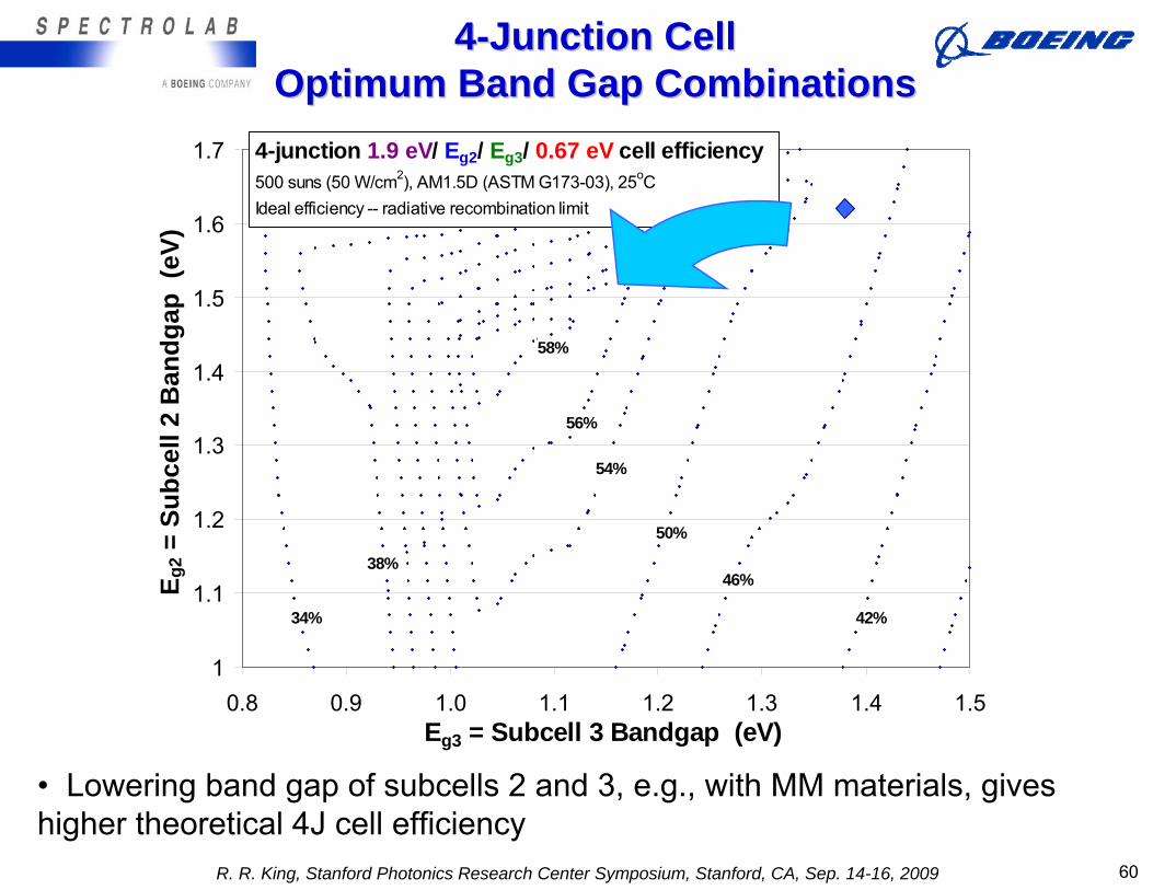
1
1.1
1.2
1.3
1.4
1.5
1.6
1.7
0.8 0.9 1.0 1.1 1.2 1.3 1.4 1.5Eg3 = Subcell 3 Bandgap (eV)
E g2 =
Sub
cell
2 B
andg
ap (
eV)
.
38%46%
54%
56%
50%
42%
4-junction 1.9 eV/ Eg2/ Eg3/ 0.67 eV cell efficiency500 suns (50 W/cm2), AM1.5D (ASTM G173-03), 25oCIdeal efficiency -- radiative recombination limitX
58%
34%
44--Junction Cell Junction Cell Optimum Band Gap CombinationsOptimum Band Gap Combinations
• Lowering band gap of subcells 2 and 3, e.g., with MM materials, gives higher theoretical 4J cell efficiency
R. R. King, Stanford Photonics Research Center Symposium, Stanford, CA, Sep. 14-16, 2009 60
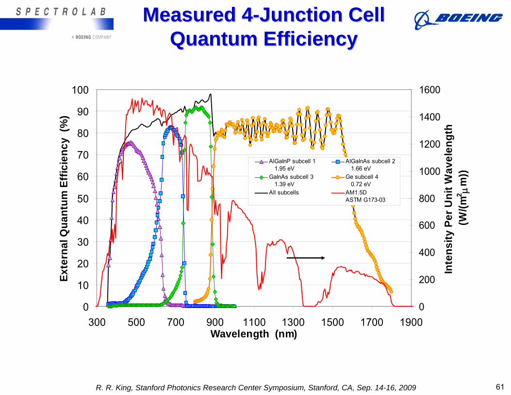
0
10
20
30
40
50
60
70
80
90
100
300 500 700 900 1100 1300 1500 1700 1900Wavelength (nm)
Exte
rnal
Qua
ntum
Eff
icie
ncy
(%)
0
200
400
600
800
1000
1200
1400
1600
Inte
nsity
Per
Uni
t Wav
elen
gth
(W
/(m2 μ
m))
AlGaInP subcell 1 1.95 eV
AlGaInAs subcell 2 1.66 eV
GaInAs subcell 3 1.39 eV
Ge subcell 4 0.72 eV
All subcells AM1.5DASTM G173-03
Measured 4Measured 4--Junction Cell Junction Cell Quantum EfficiencyQuantum Efficiency
R. R. King, Stanford Photonics Research Center Symposium, Stanford, CA, Sep. 14-16, 2009 61
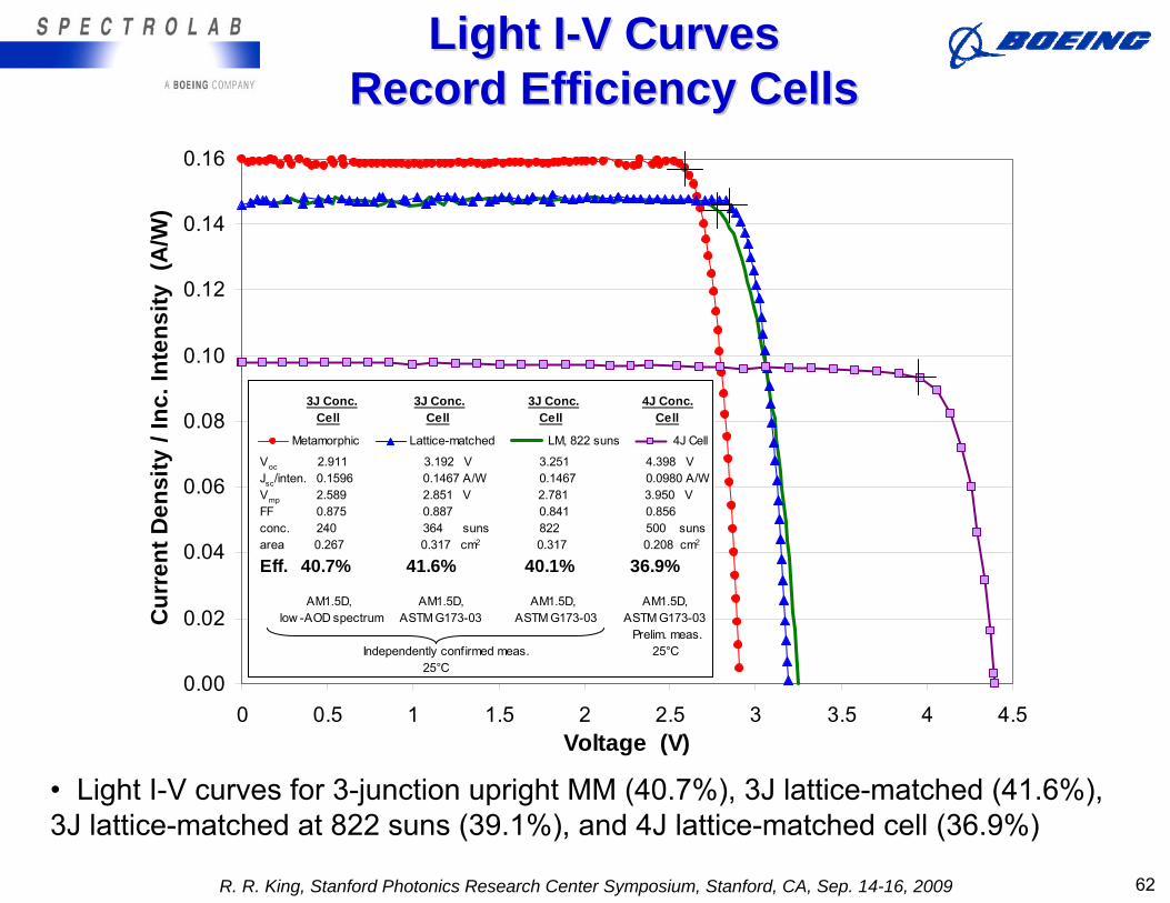
Light ILight I--V CurvesV CurvesRecord Efficiency CellsRecord Efficiency Cells
• Light I-V curves for 3-junction upright MM (40.7%), 3J lattice-matched (41.6%), 3J lattice-matched at 822 suns (39.1%), and 4J lattice-matched cell (36.9%)
0.00
0.02
0.04
0.06
0.08
0.10
0.12
0.14
0.16
0 0.5 1 1.5 2 2.5 3 3.5 4 4.5Voltage (V)
Cur
rent
Den
sity
/ In
c. In
tens
ity (
A/W
) .
Metamorphic Lattice-matched LM, 822 suns 4J Cell
3J Conc. 3J Conc. 3J Conc. 4J Conc. Cell Cell Cell Cell
Voc 2.911 3.192 V 3.251 4.398 V Jsc/inten. 0.1596 0.1467 A/W 0.1467 0.0980 A/W Vmp 2.589 2.851 V 2.781 3.950 V FF 0.875 0.887 0.841 0.856 conc. 240 364 suns 822 500 suns area 0.267 0.317 cm2 0.317 0.208 cm2
Eff. 40.7% 41.6% 40.1% 36.9%
AM1.5D, AM1.5D, AM1.5D, AM1.5D, low -AOD spectrum ASTM G173-03 ASTM G173-03 ASTM G173-03 Prelim. meas. Independently confirmed meas. 25°C 25°C
R. R. King, Stanford Photonics Research Center Symposium, Stanford, CA, Sep. 14-16, 2009 62
SemiconductorSemiconductor--Bonded Technology Bonded Technology (SBT) Terrestrial Concentrator Cell(SBT) Terrestrial Concentrator Cell
InP growth substrateGaAs or Ge growth substrate
1.4-eV GaInAs cell 3
1.7-eV AlGaInAs cell 2
2.0-eV AlGaInP cell 10.75-eV GaInAs cell 5
1.1-eV GaInPAs cell 4
GaAs or Ge growth substrate
1.4-eV GaInAs cell 3
1.7-eV AlGaInAs cell 2
2.0-eV AlGaInP cell 1
1.4-eV GaInAs cell 3
1.7-eV AlGaInAs cell 2
2.0-eV AlGaInP cell 1
GaAs or Ge growth substrate
1.4-eV GaInAs cell 3
1.7-eV AlGaInAs cell 2
2.0-eV AlGaInP cell 1
GaAs or Ge growth substrate
semi-conductor
bondedinterface
metal gridline
0.75-eV GaInAs cell 5
1.1-eV GaInPAs cell 4
1.4-eV GaInAs cell 3
1.7-eV AlGaInAs cell 2
2.0-eV AlGaInP cell 1
semi-conductor
bondedinterface
metal gridline
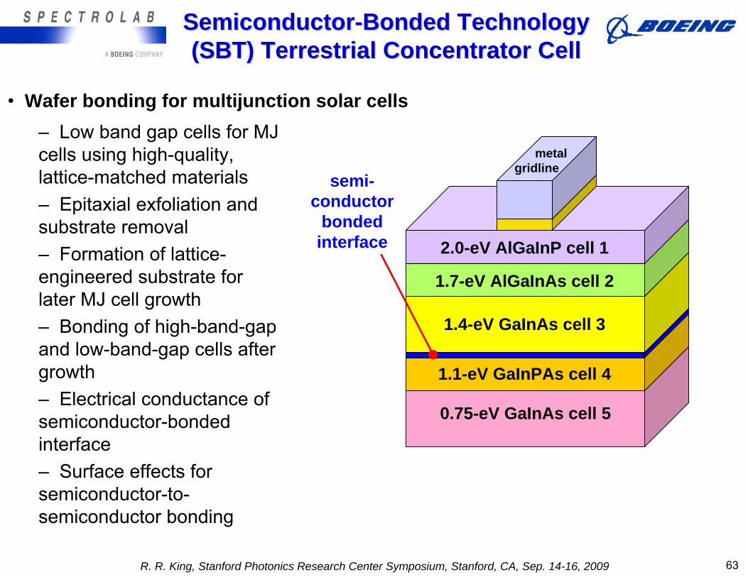
– Low band gap cells for MJ cells using high-quality, lattice-matched materials– Epitaxial exfoliation and substrate removal– Formation of lattice-engineered substrate for later MJ cell growth– Bonding of high-band-gap and low-band-gap cells after growth– Electrical conductance of semiconductor-bonded interface– Surface effects for semiconductor-to-semiconductor bonding
• Wafer bonding for multijunction solar cells
R. R. King, Stanford Photonics Research Center Symposium, Stanford, CA, Sep. 14-16, 2009 63
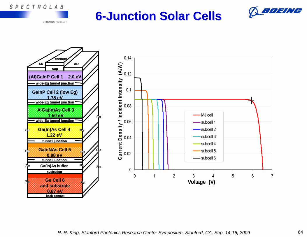
cap
contactAR
(Al)GaInP Cell 1 2.0 eVwide-Eg tunnel junction
GaInP Cell 2 (low Eg)1.78 eV
wide-Eg tunnel junction
AlGa(In)As Cell 31.50 eV
tunnel junction
Ga(In)As Cell 41.22 eV
tunnel junction
AR
Ga(In)As buffer
Ge Cell 6and substrate
0.67 eV
nucleation
back contact
wide-Eg tunnel junction
GaInNAs Cell 50.98 eV
cap
contactAR
(Al)GaInP Cell 1 2.0 eVwide-Eg tunnel junction
GaInP Cell 2 (low Eg)1.78 eV
wide-Eg tunnel junction
AlGa(In)As Cell 31.50 eV
tunnel junction
Ga(In)As Cell 41.22 eV
tunnel junction
AR
Ga(In)As buffer
Ge Cell 6and substrate
0.67 eV
nucleationnucleation
back contact
wide-Eg tunnel junction
GaInNAs Cell 50.98 eV
0
0.02
0.04
0.06
0.08
0.1
0.12
0.14
0 1 2 3 4 5 6 7Voltage (V)
Cur
rent
Den
sity
/ In
cide
nt In
tens
ity (
A/W
)MJ cellsubcell 1subcell 2subcell 3subcell 4subcell 5subcell 6
66--Junction Solar CellsJunction Solar Cells
R. R. King, Stanford Photonics Research Center Symposium, Stanford, CA, Sep. 14-16, 2009 64
0
100
200
300
400
500
600
700
0 0.5 1 1.5 2 2.5 3 3.5 4Photon Energy (eV)
Inte
nsity
per
Uni
t Pho
ton
Ener
gy(W
/m 2
. eV
)
0
0.2
0.4
0.6
0.8
1
1.2
1.4
Phot
on u
tiliz
atio
n ef
ficie
ncy
.
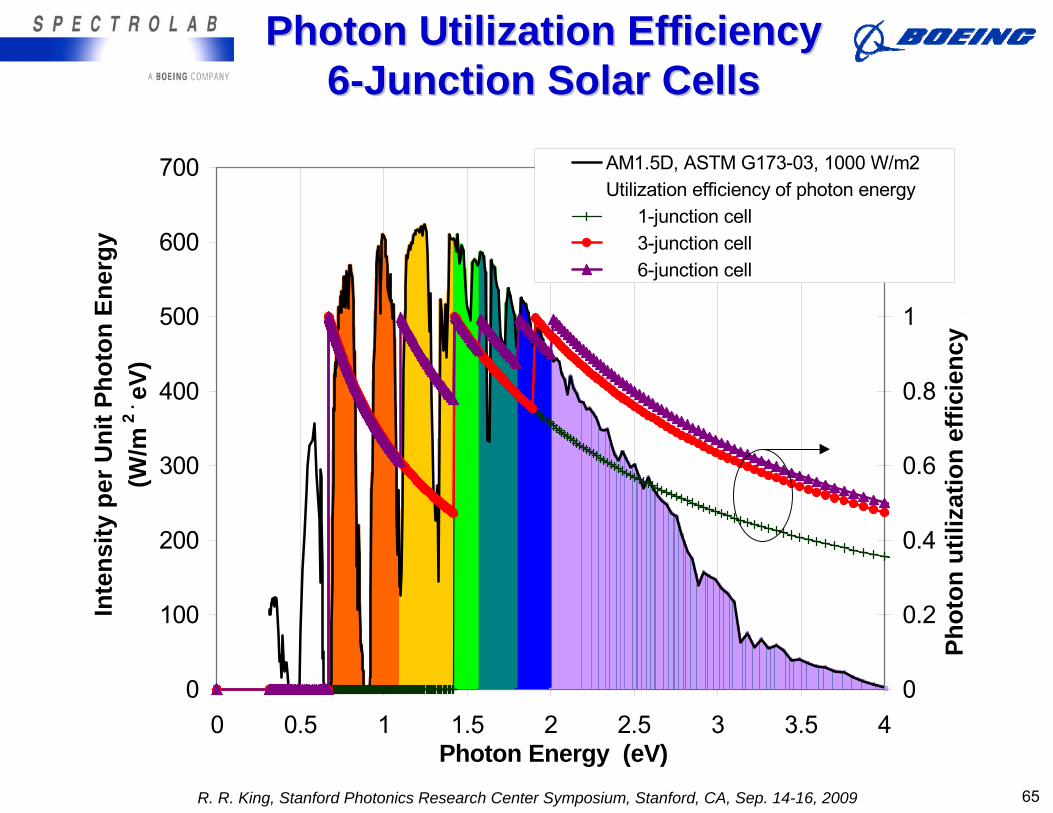
AM1.5D, ASTM G173-03, 1000 W/m2Utilization efficiency of photon energy 1-junction cell 3-junction cell 6-junction cell
Photon Utilization EfficiencyPhoton Utilization Efficiency66--Junction Solar CellsJunction Solar Cells
R. R. King, Stanford Photonics Research Center Symposium, Stanford, CA, Sep. 14-16, 2009 65
Concentrator Photovoltaic (CPV)
Systems and
Economics
R. R. King, Stanford Photonics Research Center Symposium, Stanford, CA, Sep. 14-16, 2009 66
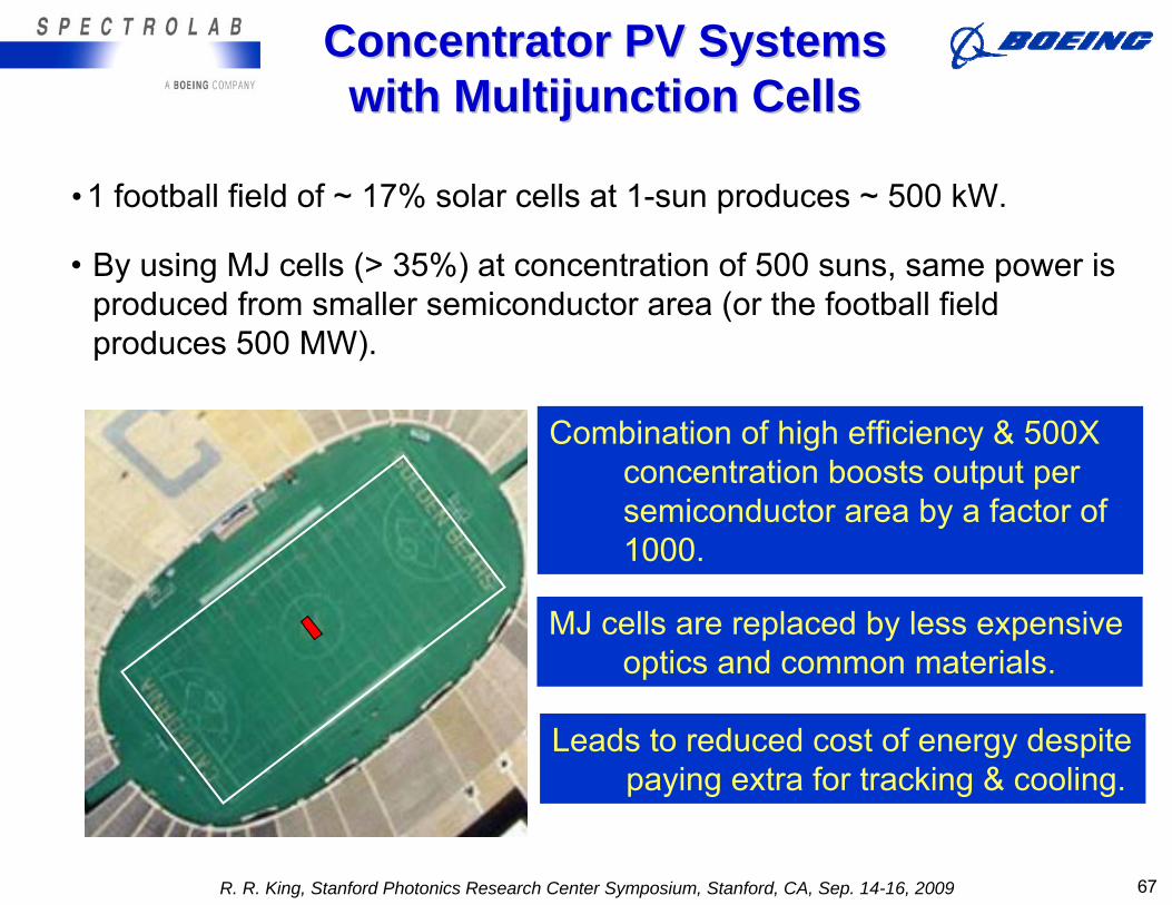
Combination of high efficiency & 500X concentration boosts output per semiconductor area by a factor of 1000.
• 1 football field of ~ 17% solar cells at 1-sun produces ~ 500 kW.
• By using MJ cells (> 35%) at concentration of 500 suns, same power is produced from smaller semiconductor area (or the football field produces 500 MW).
MJ cells are replaced by less expensive optics and common materials.
Leads to reduced cost of energy despite paying extra for tracking & cooling.
Concentrator PV Systems Concentrator PV Systems with Multijunction Cellswith Multijunction Cells
R. R. King, Stanford Photonics Research Center Symposium, Stanford, CA, Sep. 14-16, 2009 67
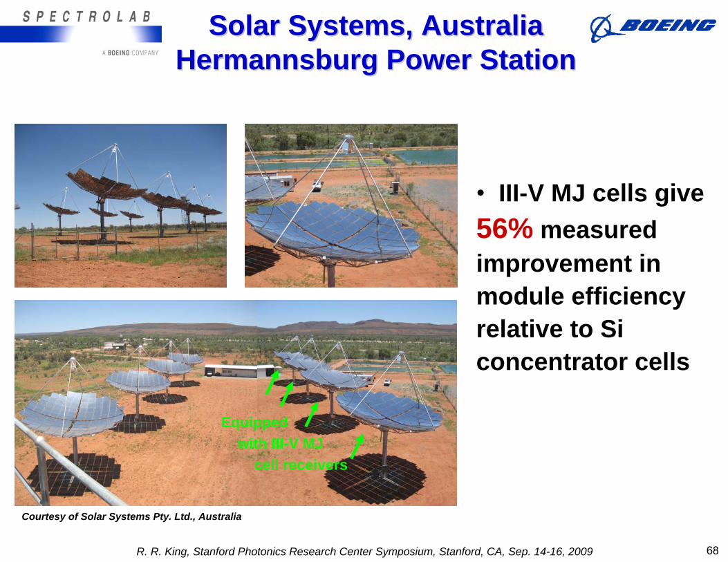
Courtesy of Solar Systems Pty. Ltd., Australia
Equipped with III-V MJ
cell receivers
• III-V MJ cells give 56% measured improvement in module efficiency relative to Si concentrator cells
Solar Systems, AustraliaSolar Systems, AustraliaHermannsburg Power StationHermannsburg Power Station
R. R. King, Stanford Photonics Research Center Symposium, Stanford, CA, Sep. 14-16, 2009 68
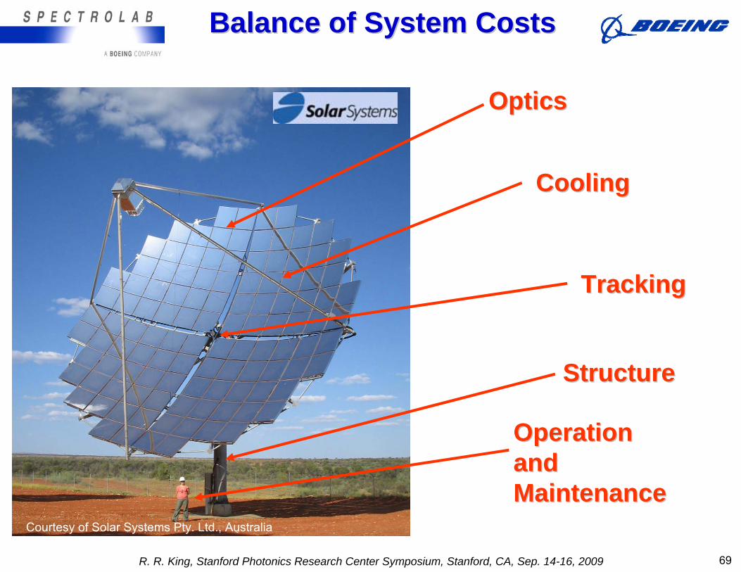
Courtesy of Solar Systems Pty. Ltd., Australia
TrackingTracking
StructureStructure
OpticsOptics
CoolingCooling
Operation Operation and and MaintenanceMaintenance
Balance of System CostsBalance of System Costs
R. R. King, Stanford Photonics Research Center Symposium, Stanford, CA, Sep. 14-16, 2009 69
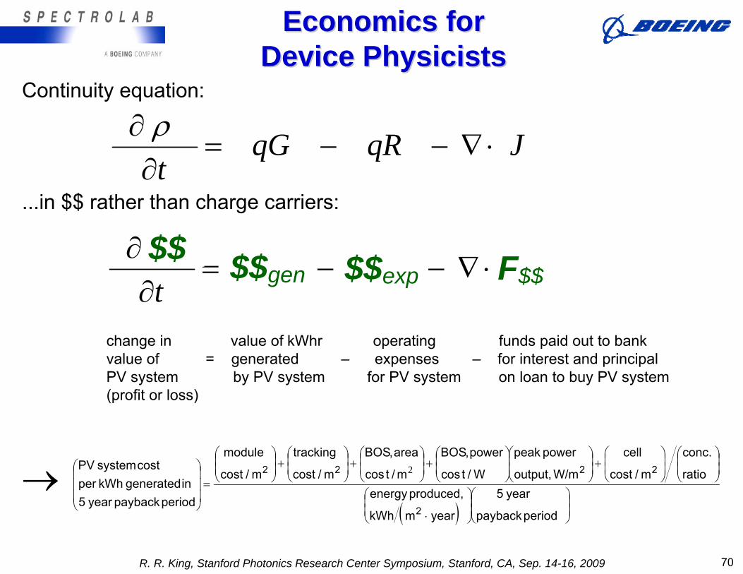
Economics for Economics for Device PhysicistsDevice Physicists
Continuity equation:
...in $$ rather than charge carriers:
change in value of kWhr operating funds paid out to bankvalue of = generated – expenses – for interest and principalPV system by PV system for PV system on loan to buy PV system(profit or loss)
→( ) ⎟
⎟⎠
⎞⎜⎜⎝
⎛⎟⎟⎠
⎞⎜⎜⎝
⎛
⋅
⎟⎟⎠
⎞⎜⎜⎝
⎛⎟⎟⎠
⎞⎜⎜⎝
⎛+⎟
⎟⎠
⎞⎜⎜⎝
⎛⎟⎟⎠
⎞⎜⎜⎝
⎛+⎟
⎟⎠
⎞⎜⎜⎝
⎛+⎟
⎟⎠
⎞⎜⎜⎝
⎛+⎟
⎟⎠
⎞⎜⎜⎝
⎛
=⎟⎟⎟
⎠
⎞
⎜⎜⎜
⎝
⎛
period payback
year5
yearm kWh
produced,energy ratio
conc.
m / cost
cell
W/moutput,
power peak
W/tcos
power,BOS
m/tcos
area,BOS
m / cost
tracking
m / cost
module
period payback year5in generated kWh per
cost systemPV
2
2222 2
J Rq Gq t
⋅∇−−=∂∂ ρ
J Rq Gq t
⋅∇−−=∂∂ ρ$$ $$gen $$exp F$$
R. R. King, Stanford Photonics Research Center Symposium, Stanford, CA, Sep. 14-16, 2009 70
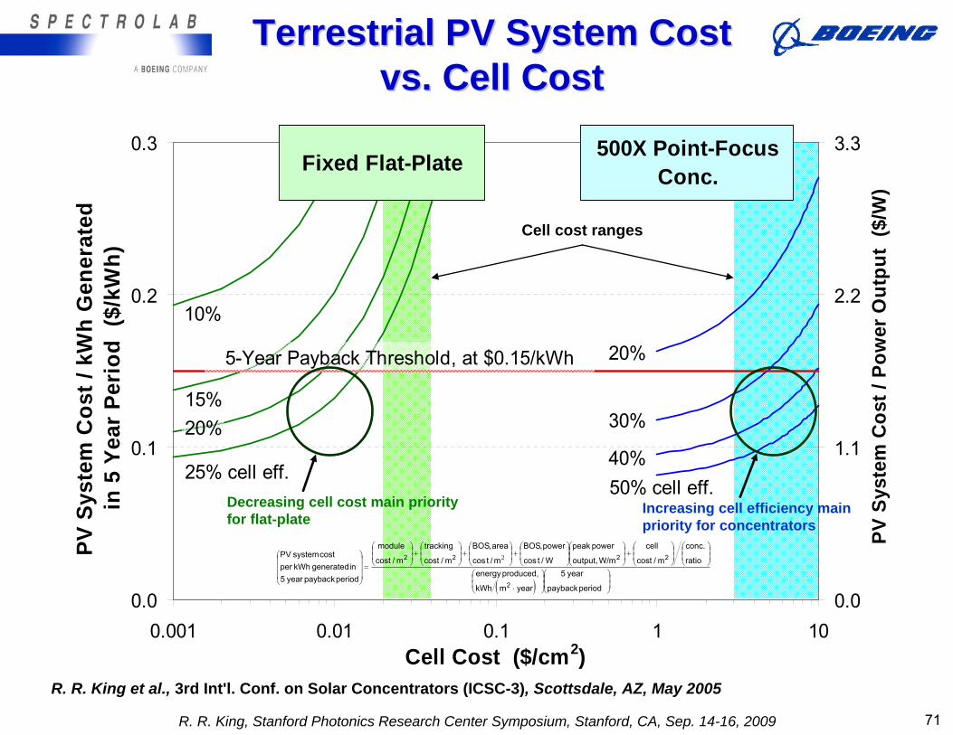
Cell cost ranges
0.0
0.1
0.2
0.3
0.001 0.01 0.1 1 10Cell Cost ($/cm2)
PV S
yste
m C
ost /
kW
h G
ener
ated
in
5 Y
ear
Peri
od (
$/kW
h)
0.0
1.1
2.2
3.3
PV S
yste
m C
ost /
Pow
er O
utpu
t ($
/W)
5-Year Payback Threshold, at $0.15/kWh
500X Point-Focus Conc.
20%
30%
40%50% cell eff.
10%
20%15%
25% cell eff.
Fixed Flat-Plate
( ) ⎟⎟⎠
⎞⎜⎜⎝
⎛⎟⎟⎠
⎞⎜⎜⎝
⎛
⋅
⎟⎟⎠
⎞⎜⎜⎝
⎛⎟⎟⎠
⎞⎜⎜⎝
⎛+⎟
⎟⎠
⎞⎜⎜⎝
⎛⎟⎟⎠
⎞⎜⎜⎝
⎛+⎟
⎟⎠
⎞⎜⎜⎝
⎛+⎟
⎟⎠
⎞⎜⎜⎝
⎛+⎟
⎟⎠
⎞⎜⎜⎝
⎛
=⎟⎟⎟
⎠
⎞
⎜⎜⎜
⎝
⎛
period payback
year5
yearm kWh
produced,energy ratio
conc.
m / cost
cell
W/moutput,
power peak
W/tcos
power,BOS
m/tcos
area,BOS
m / cost
tracking
m / cost
module
period payback year5in generated kWh per
cost systemPV
2
2222 2
R. R. King et al., 3rd Int'l. Conf. on Solar Concentrators (ICSC-3), Scottsdale, AZ, May 2005
Increasing cell efficiency main priority for concentrators
Decreasing cell cost main priority for flat-plate
Terrestrial PV System Cost Terrestrial PV System Cost vs. Cell Costvs. Cell Cost
R. R. King, Stanford Photonics Research Center Symposium, Stanford, CA, Sep. 14-16, 2009 71
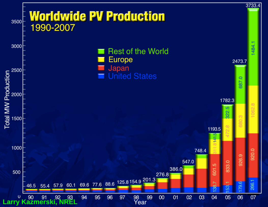
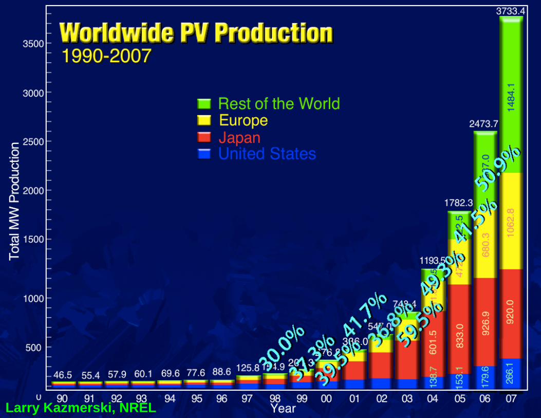
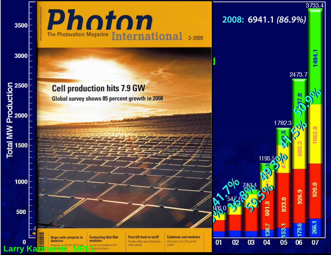
Larry Kazmerski, NREL
Larry Kazmerski, NREL
Larry Kazmerski, NREL
• Urgent global need to address carbon emission, climate change, and energy security concerns → renewable electric power can help• Theoretical solar conversion efficiency
– Examining built-in assumptions points out opportunities for higher PV efficiency– Multijunction architectures, up/down conversion, quantum structures, intermediate bands, hot-carrier effects, solar concentration → higher η– Theo. solar cell η > 70%, practical η > 50% achievable
• Metamorphic multijunction cells have begun to realize their promise– Metamorphic semiconductors offer vastly expanded of band gaps– 40.7% metamorphic GaInP/ GaInAs/ Ge 3J cells demonstrated– First solar cells of any type to reach over 40% efficiency
• New world record efficiency of 41.6% demonstrated– Highest efficiency yet measured for any type of solar cell– 41.6% efficiency independently verified at NREL (364 suns, 25°C, AM1.5D)
• Solar cells with efficiencies in this range can transform the way we generate most of our electricity, and make the PV market explode
SummarySummary
R. R. King, Stanford Photonics Research Center Symposium, Stanford, CA, Sep. 14-16, 2009 75